Chapter # 3: Multi-Level Combinational Logic - UPRMborges/Chp3.pdf · Chapter # 3: Multi-Level...
23
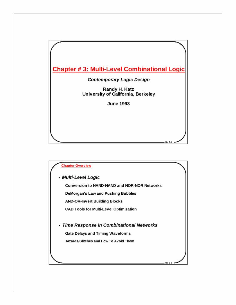
No. 3-1 Chapter # 3: Multi-Level Combinational Logic Contemporary Logic Design Randy H. Katz University of California, Berkeley June 1993 No. 3-2 Chapter Overview • Multi-Level Logic Conversion to NAND-NAND and NOR-NOR Networks DeMorgan's Law and Pushing Bubbles AND-OR-Invert Building Blocks CAD Tools for Multi-Level Optimization • Time Response in Combinational Networks Gate Delays and Timing Waveforms Hazards/Glitches and How To Avoid Them
Transcript of Chapter # 3: Multi-Level Combinational Logic - UPRMborges/Chp3.pdf · Chapter # 3: Multi-Level...
No. 3-1
Chapter # 3: Multi-Level Combinational Logic
Contemporary Logic Design
Randy H. KatzUniversity of California, Berkeley
June 1993
No. 3-2
Chapter Overview
• Multi-Level Logic
Conversion to NAND-NAND and NOR-NOR Networks
DeMorgan's Law and Pushing Bubbles
AND-OR-Invert Building Blocks
CAD Tools for Multi-Level Optimization
• Time Response in Combinational Networks
Gate Delays and Timing Waveforms
Hazards/Glitches and How To Avoid Them

No. 3-3
Boolean Algebra
Commutative Laws:
a + b = b + a a • b = b • a
Associative Laws:
(a+b)+c = a+(b+c) (ab)c = a(bc)
Identities:
a + 0 = a a • 0 = 0a • 1 = a a + 1 = 1
Distributive Laws:a + (b • c) = (a+b) • (b+c) a • (b+c) = (a • b) + (a • c)
No. 3-4
Boolean Algebra
Complement:
a + a = 1 a • a = 0
a + a = a a • a = a
Theorems:
a + ab = a ab + ab = b
DeMorgan’s Theorem:
a • b = a + b a + b = a • b
No. 3-5
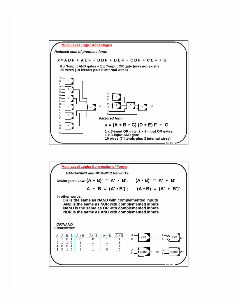
Multi-Level Logic: Advantages
Reduced sum of products form:
x = A D F + A E F + B D F + B E F + C D F + C E F + G 6 x 3-input AND gates + 1 x 7-input OR gate (may not exist!) 25 wires (19 literals plus 6 internal wires)
1
2
3
4
5
6
7
1
2 3 4
A
A
A
B
B
B
C
C
C
D
D
D
D
E
E
E
E
F
F
F
F
F
F
F
G
G
x x
Factored form:
x = (A + B + C) (D + E) F + G 1 x 3-input OR gate, 2 x 2-input OR gates, 1 x 3-input AND gate 10 wires (7 literals plus 3 internal wires)
No. 3-6
Multi-Level Logic: Conversion of Forms
NAND-NAND and NOR-NOR Networks
DeMorgan's Law: (A + B)' = A' • B'; (A • B)' = A' + B'
A + B = (A' • B')'; (A • B) = (A' + B')'In other words, OR is the same as NAND with complemented inputs AND is the same as NOR with complemented inputs NAND is the same as OR with complemented inputs NOR is the same as AND with complemented inputs
OR/NANDEquivalence
A A B B
A 0 0 1 1
A 1 1 0 0
B 0 1 0 1
B 1 0 1 0
A + B 0 1 1 1
A • B 0 1 1 1 A A
B B
A + B 1 1 1 0
A • B 1 1 1 0
≡
≡
OR OR
Nand Nand

No. 3-7
Mult-Level Logic: Conversion Between Forms
AND/NOREquivalence
It is possible to convert from networks with ANDs and ORs to networks with NANDs and NORs by introducing the appropriate inversions ("bubbles")
To preserve logic levels, each introduced "bubble" must be matched with a corresponding "bubble"
It is possible to convert from networks with ANDs and ORs to networks with NANDs and NORs by introducing the appropriate inversions ("bubbles")
To preserve logic levels, each introduced "bubble" must be matched with a corresponding "bubble"
A A B B
A 0 0 1 1
A 1 1 0 0
B 0 1 0 1
B 1 0 1 0
A • B 0 0 0 1
A + B 0 0 0 1 A A
B B
A • B 1 0 0 0
A + B 1 0 0 0
≡
≡
AND AND
NOR NOR
No. 3-8
A A B B
C C D D
A B
C D
A B
C D
Multi-Level Logic: Conversion of Forms
Example: Map AND/OR network to NAND/NAND network
NANDNAND
AND
AND
OR
NANDNAND
(A)
(C)
(B)
(D)

No. 3-9
Example: Map AND/OR network to NAND/NAND network
Z = [(A•B)' (C•D)' ]'
= [(A' + B') (C' + D')]'
= [(A' + B')' • (C' + D')']
= (A • B) + (C • D) ¦This is the easy conversion!
NAND
NAND
NAND
AA
BB
CC
DD
ZZ
No. 3-10
Example: Map AND/OR network to NOR/NOR network
Step 1 Step 2
NOR
Conserve"Bubbles"
NOR
NOR
Conserve"Bubbles"
Z =
A \A
B\B
C
\CD
\D
ZZ

No. 3-11
Example: Map AND/OR network to NOR/NOR network
Step 1 Step 2Conserve"Bubbles"
Conserve"Bubbles"
Z = {[(A' + B')' + (C' + D')']'}'
= {(A' + B') • (C' + D')}'
= (A' + B')' + (C' + D')'
= (A • B) + (C • D)
This is the hard conversion! AND/OR to NAND/NAND more naturalAND/OR to NAND/NAND more natural
NOR NOR
NOR
A \A
B\B
C
\CD
\D
ZZ
No. 3-12
Example: Map OR/AND network to NOR/NOR network
NOR
NOR
NOR
ConserveBubbles
Verify equivalenceof the two forms Z =

No. 3-13
Example: Map OR/AND network to NOR/NOR network
NOR
NOR
NOR
ConserveBubbles
Z = [(A + B)' + (C + D)']'
= {(A + B)'}' • {(C + D)'}'
= (A + B) • (C + D)
This is the easy conversion!
No. 3-14
Example: Map OR/AND network to NAND/NAND network
Step 1 Step 2
Nand
Nand
Nand
ConserveBubbles!
ConserveBubbles!

No. 3-15
Example: Map OR/AND network to NAND/NAND network
This is the hard conversion! OR/AND to NOR/NOR more naturalOR/AND to NOR/NOR more natural
Step 1 Step 2
Nand
Nand
Nand
ConserveBubbles!
ConserveBubbles!
Z = {[(A' • B')' • (C' • D')']'}'
= {(A' • B') + (C' • D')}'
= (A' • B')' • (C' • D')'
= (A + B) • (C + D)
No. 3-16
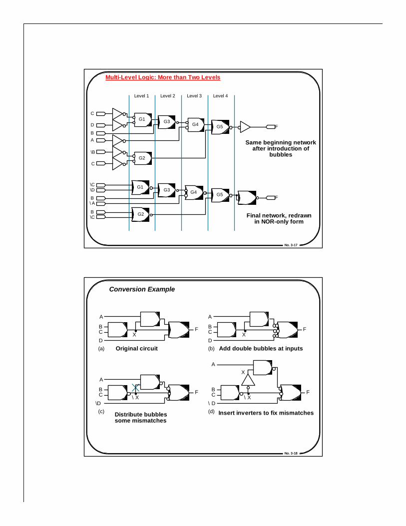
Multi-Level Logic: More than Two Levels
ƒ = A (B + C D) + B C'
OriginalAND-OR Network
Introduction and Conservation of Bubbles
Redrawn in termsof conventional
NAND Gates
C
Level 1 Level 2 Level 3 Level 4
G1 D B
A F G5 G4
G3
B G2 \ C
C G1 D
B A
F G5 G4 G3
B G2 \ C
C G1 D
\B A
F G5 G4 G3
B G2 \ C
No. 3-17
Multi-Level Logic: More than Two Levels
Same beginning networkafter introduction of
bubbles
Final network, redrawnin NOR-only form
C
Level 1 Level 2 Level 3 Level 4
G1 D
B A
F G5 G4 G3
\B
C G2
\ C G1 \ D
B \ A
F G5 G4 G3
B \ C
G2
No. 3-18
A
B C
D
F
A
B C
\D
F
X
\ X
(a) (b)
A
B C
D
F X
(d)
A
B C
\ D
F
(c)
\ X
X
Conversion Example
Original circuit Add double bubbles at inputs
Distribute bubblessome mismatches
Insert inverters to fix mismatches

No. 3-19
Multi-Level Logic: AND-OR-Invert Block (AOI)
AOI Function: Three stage logic — AND, OR, Invert Multiple gates "packaged" as a single circuit block
AND OR Invert
logical concept
two-input two-stack
A B
C D
Z
T rue A C
B D Z
False
A B
C D
No. 3-20
&
&
+2x2 AOI Schematic
Symbol
&
&
+3x2 AOI SchematicSymbol
Multi-Level Logic: AND-OR-Invert Block (AOI)

No. 3-21
Example: XOR implementation
A xor B = A' B + A B'
= ( ? )'
(A' B + A B')'
(A + B') (A' + B)
(A B + A' B')
AOI form
General procedure to place in AOI form: Compute the complement in Sum of Products form by circling the 0's in the K-map!
ƒ = (A' B' + A B)'
No. 3-22
F = B C' + A C' + A B
F' = A' B' + A' C + B' C
2-input 3-stack AOI gate
F = (A + B) (A + C') (B + C')
F' = (B' + C) (A' + C) (A' + B')
2-input 3-stack OAI gate
Example:
10 1
1
0 0 0
0 1 1
B
11 01 00 AB A
C 0
1
F K-map
No. 3-23
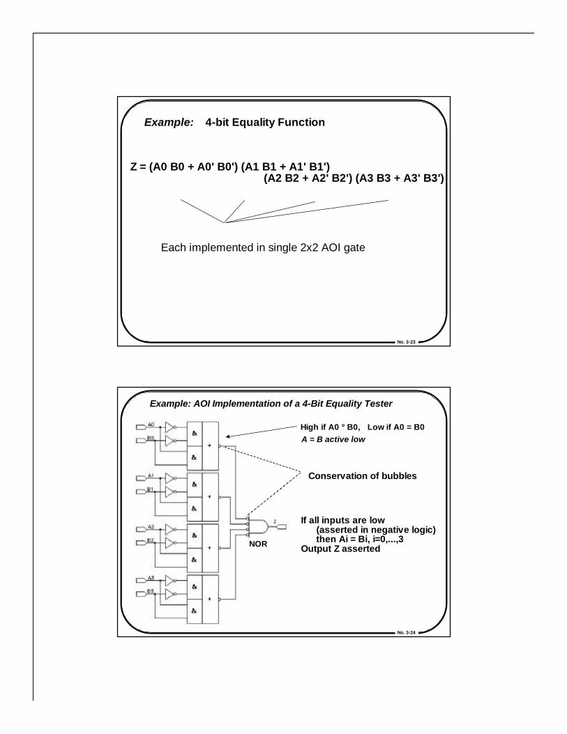
Example: 4-bit Equality Function
Z = (A0 B0 + A0' B0') (A1 B1 + A1' B1') (A2 B2 + A2' B2') (A3 B3 + A3' B3')
Each implemented in single 2x2 AOI gate
No. 3-24
Example: AOI Implementation of a 4-Bit Equality Tester
High if A0 ° B0, Low if A0 = B0A = B active low
NOR
If all inputs are low (asserted in negative logic) then Ai = Bi, i=0,...,3Output Z asserted
Conservation of bubbles

No. 3-25
Multi-Level Logic: CAD Tools for Simplification
Multi-Level Optimization:1. Factor out common sublogic (reduce fan-in, increase gate levels), subject to timing constraints
2. Map factored form onto library of gates
3. Minimize number of literals (correlates with number of wires)
Factored Form:sum of products of sum of products . . .
X = (A B + B' C) (C + D (E + A C')) + (D + E)(F G)
A
B B
C C D
E
A
C
F
G D
E
F 1
F 2
F 5 F 4
F 3
X
+
+
+
+
+
•
• • •
•
• •
No. 3-26
Multi-Level Logic: CAD Tools for Simplification
Operations on Factored Forms:• Decompostion
• Extraction
• Factoring
• Substitution
• Collapsing
Manipulate network by interactivelyissuing the appropriate instructions
There exists no algorithm that guarantees"optimal" multi-level network will be obtained

No. 3-27
Time Response in Combinational Networks• emphasis on timing behavior of circuits
• waveforms to visualize what is happening
• simulation to create these waveforms
• momentary change of signals at the outputs: hazards - can be useful— pulse shaping circuits - can be a problem — glitches: incorrect circuit operation
Terms:
gate delay - time for change at input to cause change at output minimum delay vs. typical/nominal delay vs. maximum delay careful designers design for the worst case!
rise time - time for output to transition from low to high voltage
fall time - time for output to transition from high to low voltage
No. 3-28
Pulse Shaping Circuit
A' • A = 0
F is not always 0!
3 gate delays
D remains high forthree gate delays after
A changes from low to high

No. 3-29
Another Pulse Shaping Circuit
Initially undefined
Close Switch Open Switch
+
A B
C DOpenSwitch
Resistor
No. 3-30
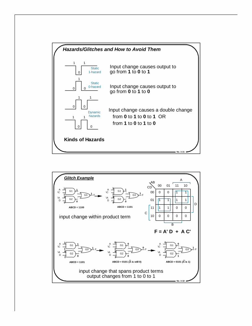
Hazards/Glitches and How to Avoid Them
Unwanting switching at the outputs
Occur because delay paths through the circuit experience different propagation delays
Danger if logic "makes a decision" while output is unstable OR hazard output controls an asynchronous input (these respond immediately to changes rather than waiting for a synchronizing signal called a clock)
Usual solutions: - wait until signals are stable (by using a clock) - never, never, never use circuits with asynchronous inputs - design hazard-free circuits
Suggest that first two approaches be used, but we'll tell youabout hazard-free design anyway!
No. 3-31
Hazards/Glitches and How to Avoid Them
Kinds of Hazards
Input change causes output togo from 1 to 0 to 1
Input change causes output togo from 0 to 1 to 0
Input change causes a double change from 0 to 1 to 0 to 1 OR from 1 to 0 to 1 to 0
Static 0-hazard
Dynamic hazards
Static 1-hazard
1 1
0
1
0 0
1
0 0
1
1 1
0 0
No. 3-32
Glitch Example
F = A' D + A C'
input change within product term
input change that spans product termsoutput changes from 1 to 0 to 1
G1
G2
G3
A\C
\AD
F
G1
G2
G3
A\C
\AD
F
1
1
11
0
0
0
1
1
11
0
0
0
ABCD = 1100 ABCD = 1101
G1
G2
G3
A\C
\AD
F
G1
G2
G3
A\C
\AD
F
0
1
00
1
0
0
1
1
11
1
0
0
ABCD = 1101 ABCD = 0101 (A is still 0)
G1
G2
G3
A\C
\AD
F
0
1
01
1
1
1
ABCD = 0101 (A is 1)
A AB
00 01 11 10
0 0 1 1
1 1 1 1
1 1 0 0
0 0 0 0
00
01
11
10 C
CD
D
B
No. 3-33
Glitch Example
General Strategy: add redundant terms
F = A' D + A C' becomes A' D + A C' + C' D
This eliminates 1-hazard? How about 0-hazard?
Re-express F in PoS form:
F = (A' + C')(A + D)
Glitch present!
Add term: (C' + D)
This expression is equivalentto the hazard-free SoP form of F
A AB 00 01 11 10
0 0 1 1
1 1 1 1
1 1 0 0
0 0 0 0
00
01
11
10 C
CD
D
B
No. 3-34
Glitch Example
Start with expression that is free of static 1-hazardsF = A C' + A' D + C' D
F' = (A C' + A' D + C' D)'
= (A' + D) (A + D') (C + D')
= A C + A C D' + C D' + A' C D' + A' D'
= A C + C D' + A' D’
covers all the adjacent 0's in the K-map
free of static-1 and static-0 hazards!
Work with complement:
No. 3-35
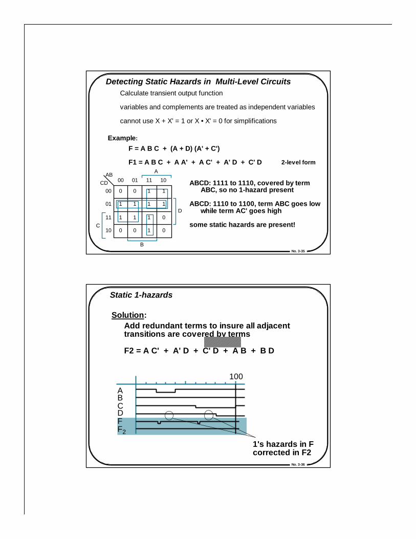
Detecting Static Hazards in Multi-Level CircuitsCalculate transient output function
variables and complements are treated as independent variables
cannot use X + X' = 1 or X • X' = 0 for simplifications
F = A B C + (A + D) (A' + C')
F1 = A B C + A A' + A C' + A' D + C' D
Example:
2-level form
ABCD: 1111 to 1110, covered by term ABC, so no 1-hazard present
ABCD: 1110 to 1100, term ABC goes low while term AC' goes high
some static hazards are present!
A AB 00 01 11 10
0 0 1 1
1 1 1 1
1 1 1 0
0 0 1 0
00
01
11
10 C
CD
D
B
No. 3-36
100
A B C D F F 2
Static 1-hazards
Solution:Add redundant terms to insure all adjacent transitions are covered by terms
F2 = A C' + A' D + C' D + A B + B D
1's hazards in Fcorrected in F2

No. 3-37
Static 0-Hazards
Similar to previous case, but work with the complement of F
If terms of the transient output function cover all 0 transitions, then no 0-hazards are present
F = [A B C + (A + D) (A' + C')]'
= (A' + B' + C') (A' D' + A C)
= A' D' + A' B D' + A' C D' + A B' C
= A' D' + A B' C
0-hazard on transition from1010 to 0010
+ B' C D'
F = (A + D) (A' + B + C') (B + C' + D)
0-hazard free
equivalent to F2 on last slide
A AB 00 01 11 10
0 0 1 1
1 1 1 1
1 1 1 0
0 0 1 0
00
01
11
10 C
CD
D
B
No. 3-38
100
A B C D F F 3
Static 0-Hazards
0-HazardCorrected in F3
No. 3-39
Designing Networks for Hazard-free operation
Simply place transient output function in a form thatguarantees that all adjacent ones are covered by a term
no term of the transient output function contains both a variable and its complement
F(A,B,C,D) = •m(1,3,5,7,8,9,12,13,14,15)
F = A B + A' D + B D + A C' + C' D
= (A' + B + C') D + A (B + C')
(factored by distributive law, which does notintroduce hazards since it does not depend onthe complementarity laws for its validity)
A AB 00 01 11 10
0 0 1 1
1 1 1 1
1 1 1 0
0 0 1 0
00
01
11
10 C
CD
D
B
No. 3-40
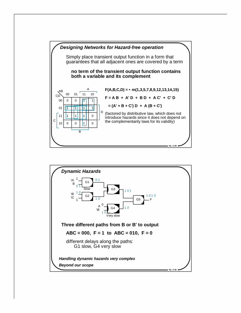
Dynamic Hazards
Three different paths from B or B' to output
ABC = 000, F = 1 to ABC = 010, F = 0
different delays along the paths: G1 slow, G4 very slow
Handling dynamic hazards very complex
Beyond our scope
G1
G2
G3
G5
G4
\A B
\B
\B \C F
A
0 1
1
1 0
1
0 1
1 0
1 0 1
1 0 0
1 0
1 0 1 0
Slow
V ery slow

No. 3-41
Elements of a Data Sheet
A data sheet contains all the relevant documentation thatyou need to use the component:
1. Description of Function2. A function/truth table3. A logic schematic with labeled I/Os4. Boolean expression of function in terms of I/Os5. Alternative package pint-outs6. Internal transistor shcematics7. Operating specifications8. Recommended operating conditions9. Electrical characteristics.10. Switching characteristics.
No. 3-42
Operating Specifications: the absolute worst-case conditionsunder which the component can operate or be stored. Maxinput volt: 7v, Temp: 0 to 70 C.
Recommended Operating Conditions: the normal operatingconditions for the supply voltage, input voltages, outputcurrents, and temperature.
VHI: min input volt recognized as a logic 1 (2v)
V IL: max input volt recognized as a logic 0 (0.8v)
IOH: max current gate can supply to maintain volt of logic 1 (-0.4 mA)
IOL: min current gate can supply to maintain volt of logic 0 (8 mA)
No. 3-43
Electrical Characteristics: voltages and currents that canbe observed at the inputs and outputs.
VOH: min output high volt (2.7v min, 3.4v typical) VOL: max output low volt (0.4v max, 0.25v typical)
IIH: max current into input when high (20uA) IIL: max current into input when low (-0.4 mA)
The voltages determine the noise margin: 0.7v marginon logic 1, and 0.4v on logic 0.
Switching Characteristics: the typical and maximumgatdelays under specified test conditions.
tPLH: delay from low to high (9ns typical, 15ns worst) tPHL: delay from high to low (10ns typical, 15ns worst)
No. 3-44
Fan-Out: a given output can drive only a finite number ofinputs before the output signal levels become degradedand are no longer recognized as good logic 1/0s.
To determine the fan-out examine the IOH of the drivinggate. This value must exceed the sum of the IIH values ofthe inputs that the gate is driving.
Similarly, the IOL of the gate must exceed the sum of theIIL values of the inputs to which it is connected.
Example: IIH: 20uA, IOH: -0.4mAIIL: -0.4mA, IOL: 8mA
It can drive 20 gates to logic 1 and to logic 0.

No. 3-45
Technology Metrics
There are differences in the underlying technologies thatmay make one technology more attractive than another.The main technology metrics are:
1. Gate Delay: the time delay between the changes. Omgeneral, bipolar techs are faster than MOS (ECL thefastest).
2. Degree of Integration: the area required to implement agiven function in the underlying tech. MOS pack much moredensely than bipolar.
SSI: up to 10 gates MSI: up to 100 gates (not important)
LSI / VLSI: up to 1000 gates (MOS has advantage)
No. 3-46
3. Power Dissipation: the power consumption and heatgenerated that must be dissipated.
- Bipolar generate more heat and consume more power - ECL consume the most power - MOS, especially CMOS, consume very little power
4. Noise Margin: the max volt that can be added to orsubtracted from the login voltages and still have the cktinterpret the voltage as the correct logic value.
- Modern TTL / CMOS have good noise margins - ECL has tighter noise margin
5. Component Cost: TTL, MOS, ECL