Chapter 3 How transistors operate and form simple switches CMOS logic gates PLA, PAL, FPGA Basic...
59
Chapter 3 • How transistors operate and form simple switches • CMOS logic gates • PLA, PAL, FPGA • Basic electrical characteristics of logic circuits
-
Upload
hester-bennett -
Category
Documents
-
view
245 -
download
5
Transcript of Chapter 3 How transistors operate and form simple switches CMOS logic gates PLA, PAL, FPGA Basic...
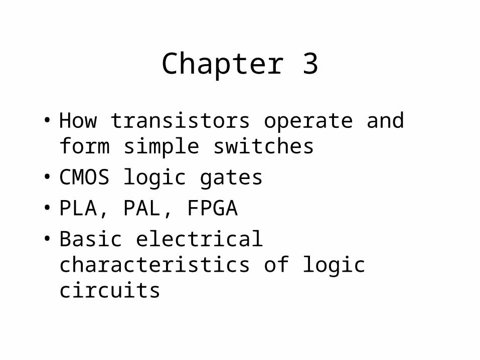
Chapter 3
• How transistors operate and form simple switches
• CMOS logic gates
• PLA, PAL, FPGA
• Basic electrical characteristics of logic circuits
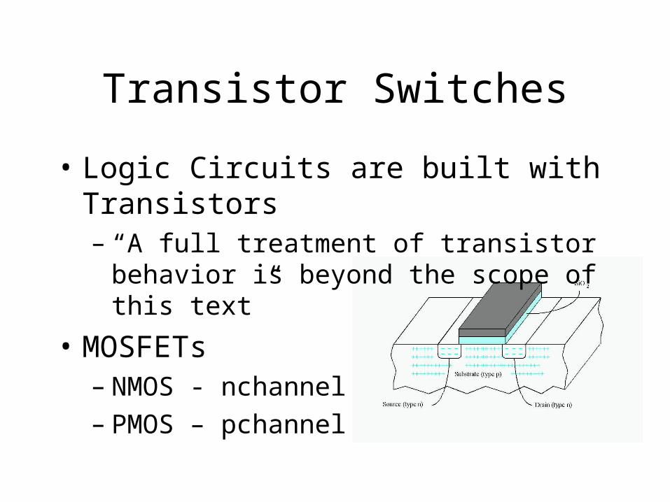
Transistor Switches
• Logic Circuits are built with Transistors– “A full treatment of transistor behavior is
beyond the scope of this text”
• MOSFETs– NMOS - nchannel– PMOS – pchannel
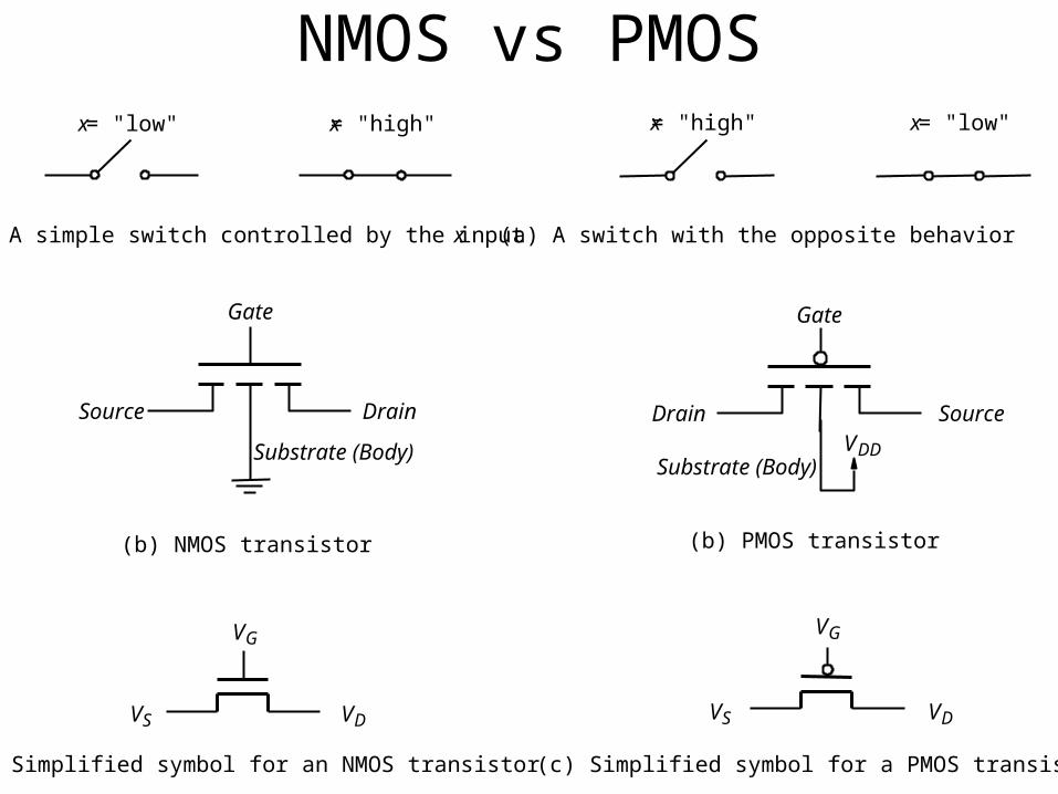
NMOS vs PMOS
Drain Source
x = "low" x = "high"
(a) A simple switch controlled by the input x
V D V S
(b) NMOS transistor
Gate
(c) Simplified symbol for an NMOS transistor
V G
Substrate (Body)
Gate
x = "high" x = "low"
(a) A switch with the opposite behavior
V G
V D V S
(b) PMOS transistor
(c) Simplified symbol for a PMOS transistor
V DD
Drain Source
Substrate (Body)
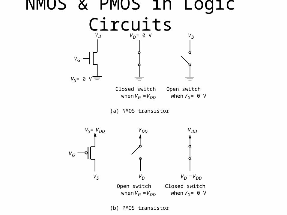
NMOS & PMOS in Logic Circuits
(a) NMOS transistor
V G
V D
V S = 0 V
V S = V DD
V D
V G
Closed switch whenV G =V DD
V D = 0 V
Open switch whenV G = 0 V
V D
Open switch whenV G =V DD
V D
V DD
Closed switch whenV G = 0 V
V D =V DD
V DD
(b) PMOS transistor
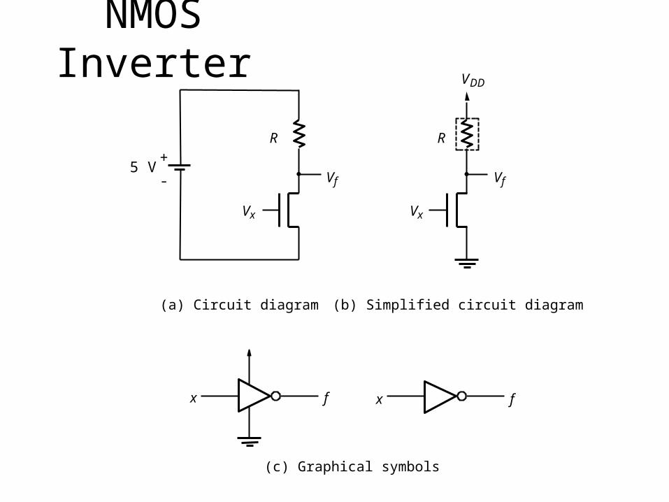
NMOS Inverter
(b) Simplified circuit diagram
V x
V f
V DD
x f
(c) Graphical symbols
x f
R
V x
V f
R +
-
(a) Circuit diagram
5 V
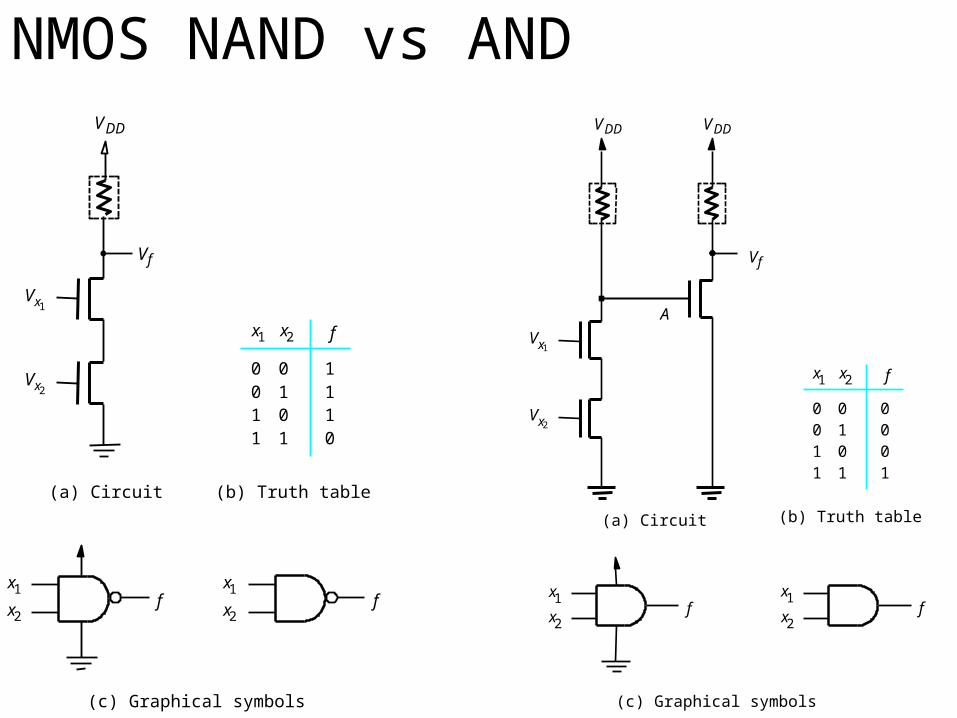
NMOS NAND vs AND
V f
V DD
(a) Circuit
(c) Graphical symbols
(b) Truth table
f f
0 0 1 1
0 1 0 1
1 1 1 0
x 1 x 2 f
V x 2
V x 1
x 1
x 2
x 1
x 2
(a) Circuit
(c) Graphical symbols
(b) Truth table
f f
0 0 1 1
0 1 0 1
0 0 0 1
x 1 x 2 f
V f
V DD
A
V x 1
V x 2
x 1
x 2
x 1
x 2
V DD
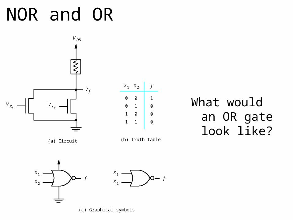
NOR and OR
What would an OR gate look like?
V x 1 V x 2
V f
V DD
(a) Circuit
(c) Graphical symbols
(b) Truth table
f
0
0
1
1
0
1
0
1
1
0
0
0
x 1 x 2 f
f x 1
x 2
x 1
x 2
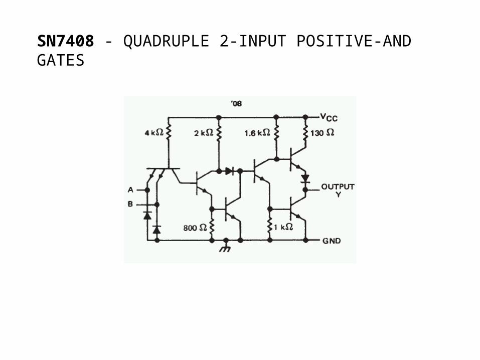
SN7408 - QUADRUPLE 2-INPUT POSITIVE-AND GATES
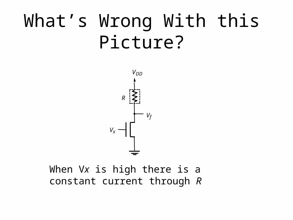
What’s Wrong With this Picture?
V x
V f
V DD
R
When Vx is high there is a constant current through R
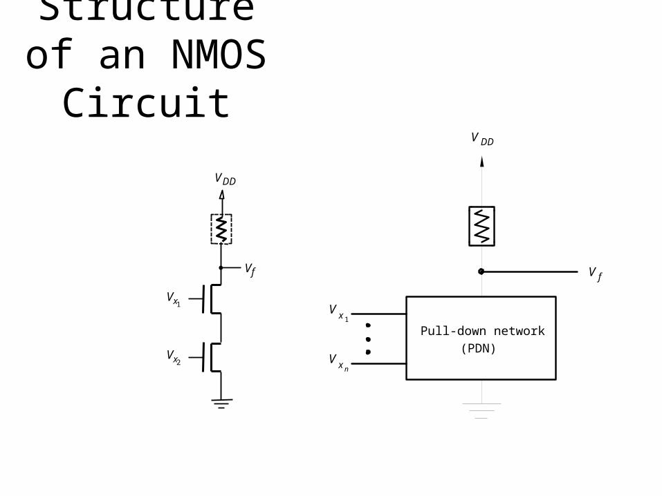
Structure of an NMOS Circuit
V f
V DD
V x 2
V x 1
V f
V DD
Pull-down network
V x 1
V x n
(PDN)
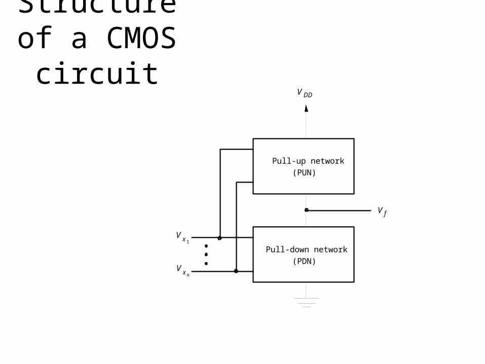
Structure of a CMOS circuit
V f
V DD
Pull-down network
Pull-up network
V x 1
V x n
(PUN)
(PDN)
V f
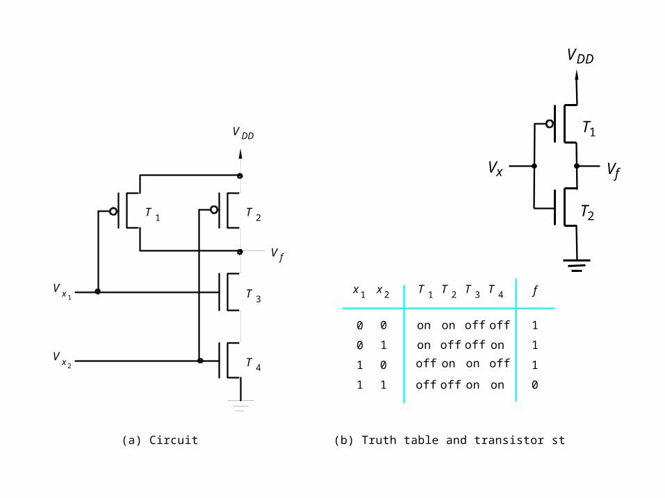
V DD
V x
T 1
T 2
(a) Circuit
V f
V DD
(b) Truth table and transistor states
on
on
on
off
0
1 0
0
1
1
0
1
off
off
on
off
off
on
f
off
on
1
1
1
0
off
off on
on
V x 1
V x 2
T 1 T 2
T 3
T 4
x 1 x 2 T 1 T 2 T 3 T 4
V f
V DD
V x 1
V x 2
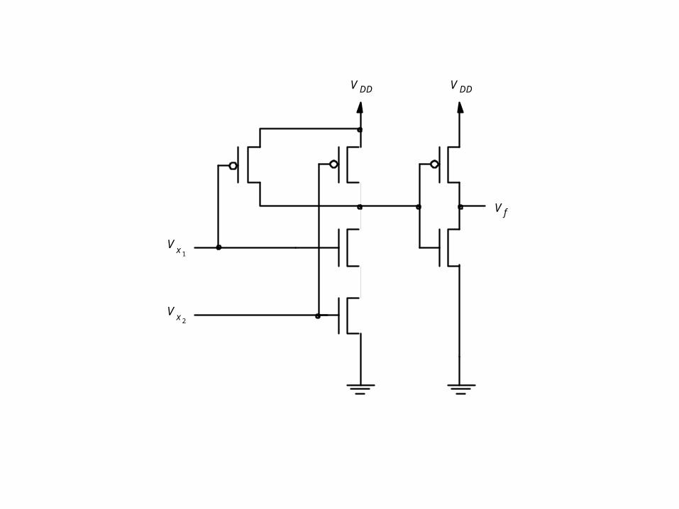
V DD
V f
V DD
V x 1
V x 2
V DD
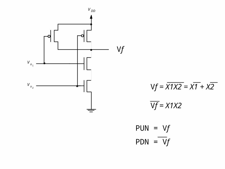
Vf
Vf = X1X2 = X1 + X2
Vf = X1X2
PUN = Vf
PDN = Vf
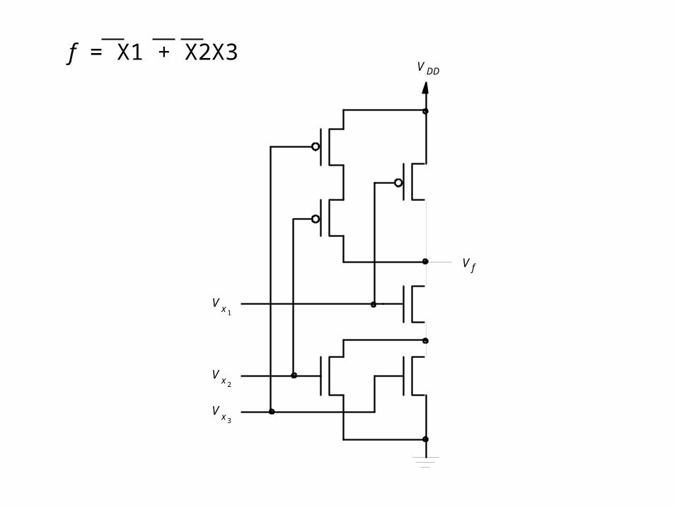
f = X1 + X2X3
V f
V DD
V x 1
V x 2
V x 3
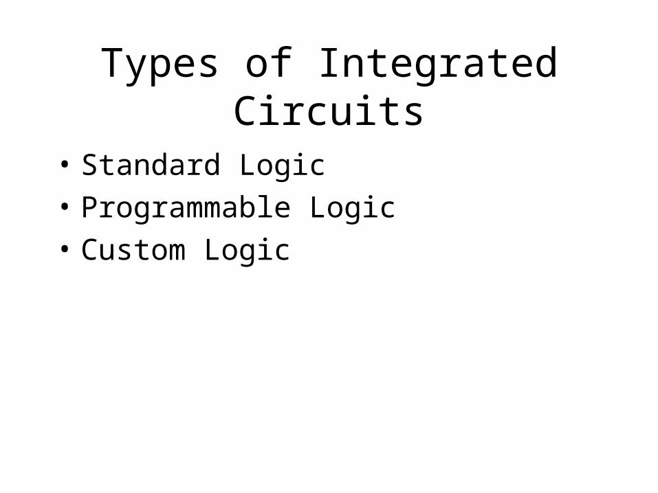
Types of Integrated Circuits
• Standard Logic
• Programmable Logic
• Custom Logic
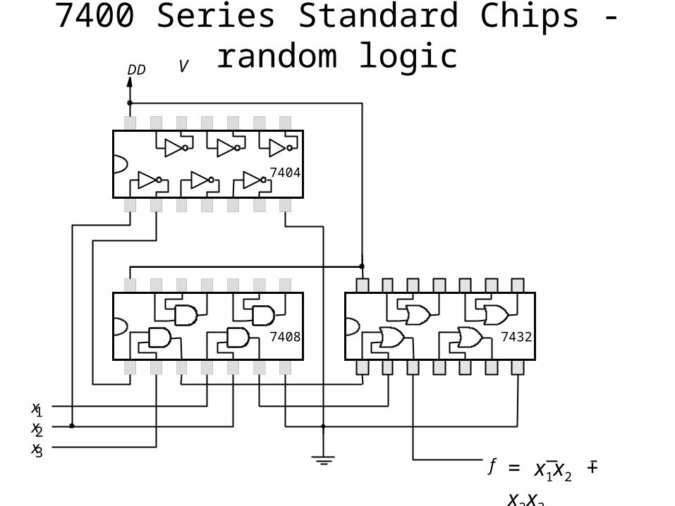
7400 Series Standard Chips - random logicV DD
x 1 x 2 x 3
f
7404
7408 7432
= x1x2 + x2x3
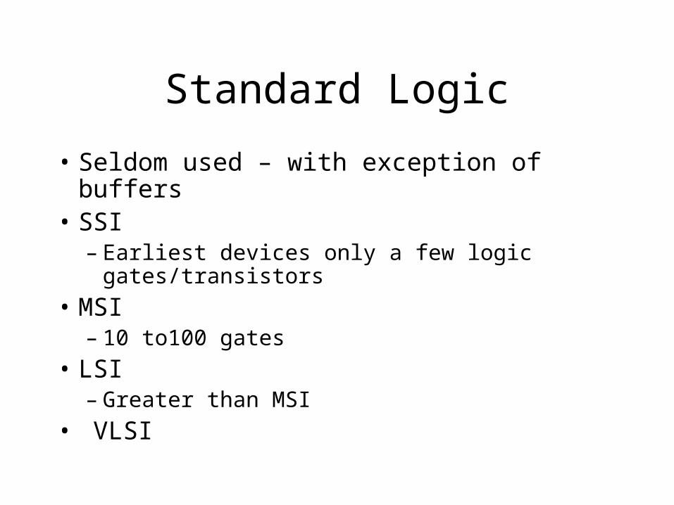
Standard Logic
• Seldom used – with exception of buffers• SSI
– Earliest devices only a few logic gates/transistors
• MSI– 10 to100 gates
• LSI– Greater than MSI
• VLSI
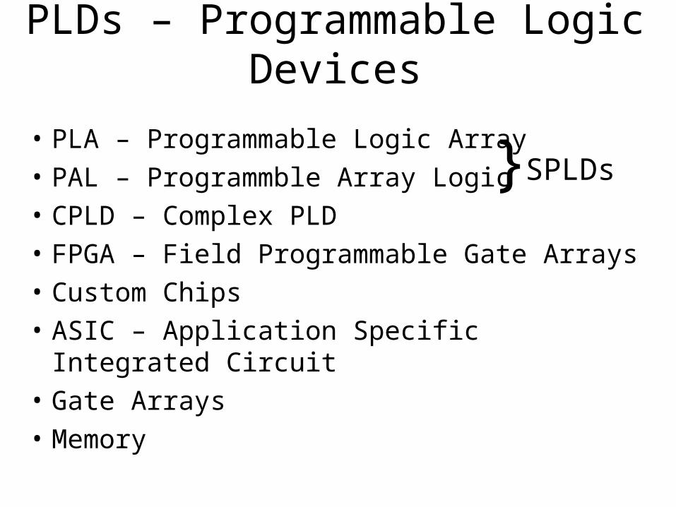
PLDs – Programmable Logic Devices
• PLA – Programmable Logic Array
• PAL – Programmble Array Logic
• CPLD – Complex PLD
• FPGA – Field Programmable Gate Arrays
• Custom Chips
• ASIC – Application Specific Integrated Circuit
• Gate Arrays
• Memory
SPLDs}
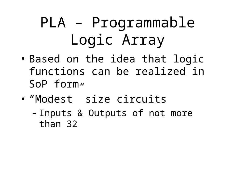
PLA – Programmable Logic Array
• Based on the idea that logic functions can be realized in SoP form
• “Modest” size circuits– Inputs & Outputs of not more than 32
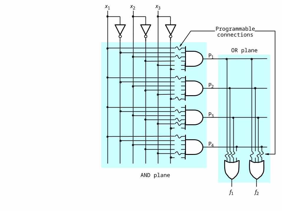
f1
P1
P2
f2
x1 x2 x3
OR plane
Programmable
AND plane
connections
P3
P4
f1
P1
P2
f2
x1 x2 x3
OR plane
Programmable
AND plane
connections
P3
P4
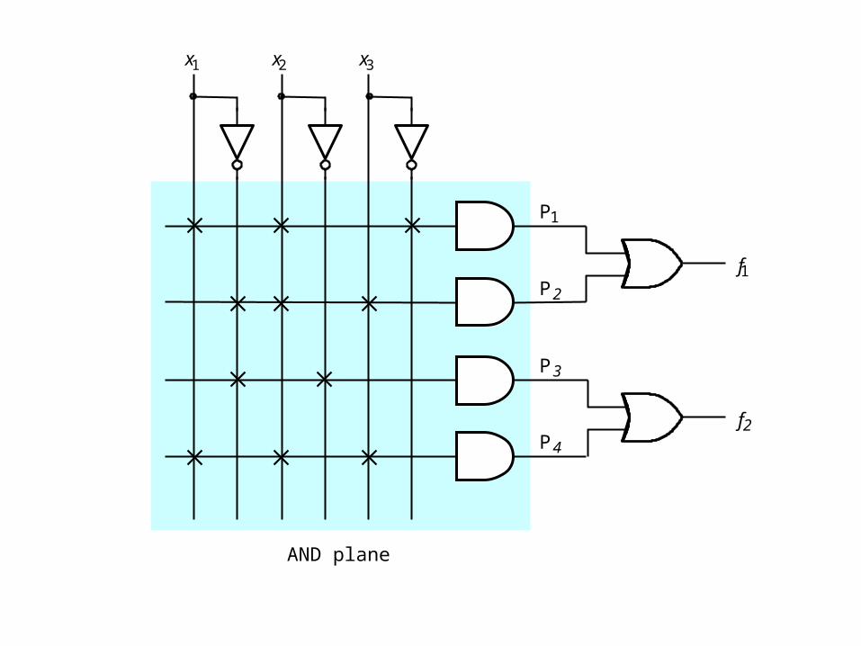
f1 = x1x2 + x1x3 + x1x2x3
f2 = x1x2 + x1x2x3 + x1x2
f 1
P 1
P 2
f 2
x 1 x 2 x 3
OR plane
AND plane
P 3
P 4
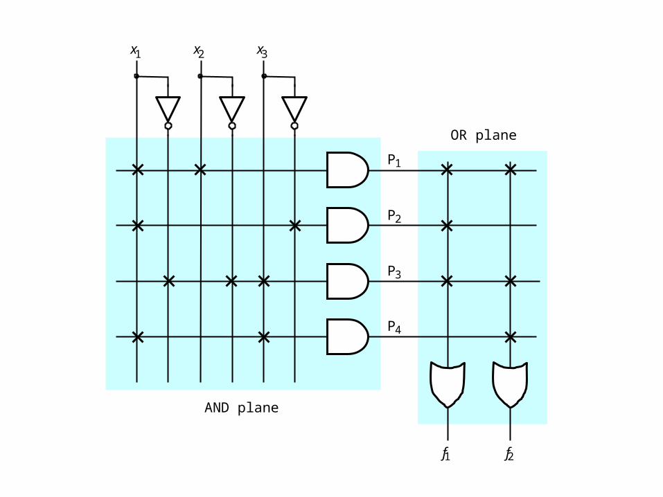
PAL – Programmble Array Logic
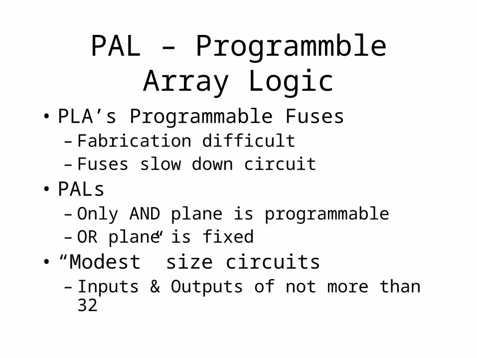
• PLA’s Programmable Fuses– Fabrication difficult– Fuses slow down circuit
• PALs– Only AND plane is programmable– OR plane is fixed
• “Modest” size circuits– Inputs & Outputs of not more than 32
f 1
P 1
P 2
f 2
x 1 x 2 x 3
AND plane
P 3
P 4
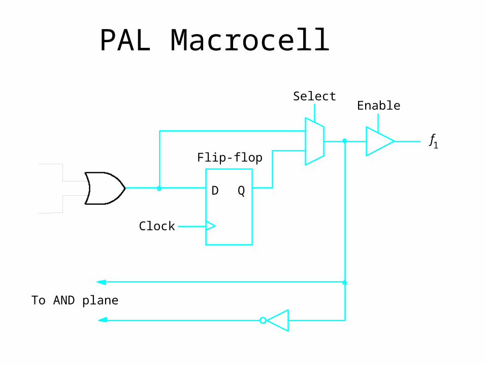
PAL Macrocell
f 1
To AND plane
D Q
Clock
SelectEnable
Flip-flop
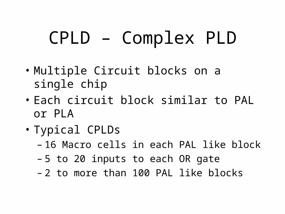
CPLD – Complex PLD
• Multiple Circuit blocks on a single chip
• Each circuit block similar to PAL or PLA
• Typical CPLDs– 16 Macro cells in each PAL like block– 5 to 20 inputs to each OR gate– 2 to more than 100 PAL like blocks
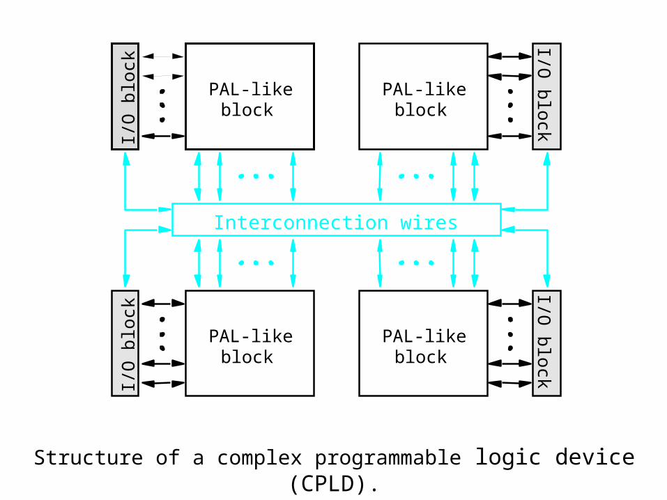
Structure of a complex programmable logic device (CPLD).
PAL-likeblock
I/O
blo
ck
PAL-likeblock
I/O b
lock
PAL-likeblock
I/O
blo
ck
PAL-likeblock
I/O b
lock
Interconnection wires
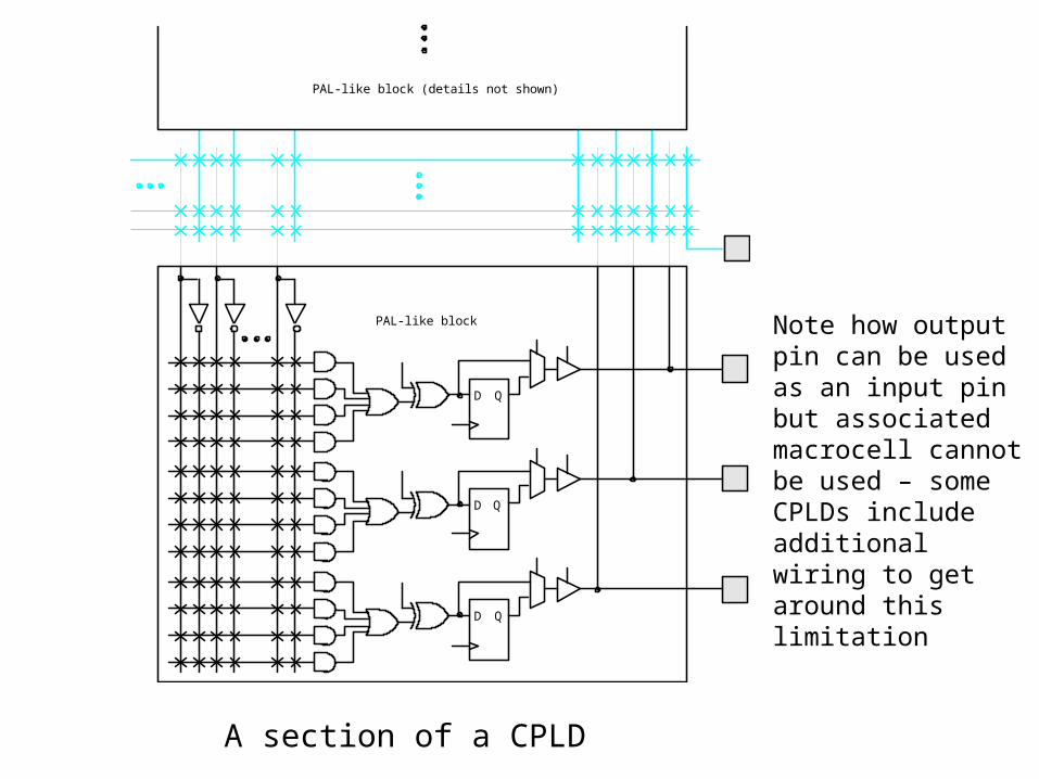
A section of a CPLD
D Q
D Q
D Q
PAL-like block (details not shown)
PAL-like block Note how output pin can be used as an input pin but associated macrocell cannot be used – some CPLDs include additional wiring to get around this limitation
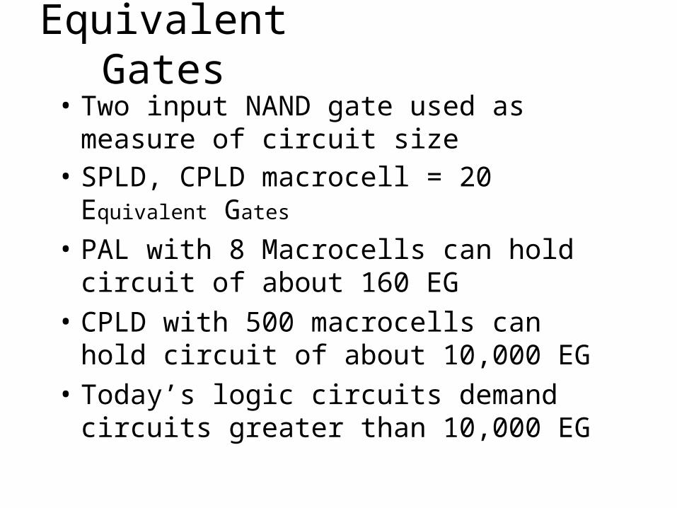
Equivalent Gates
• Two input NAND gate used as measure of circuit size
• SPLD, CPLD macrocell = 20 Equivalent Gates
• PAL with 8 Macrocells can hold circuit of about 160 EG
• CPLD with 500 macrocells can hold circuit of about 10,000 EG
• Today’s logic circuits demand circuits greater than 10,000 EG
Memory as Logic
Address Data
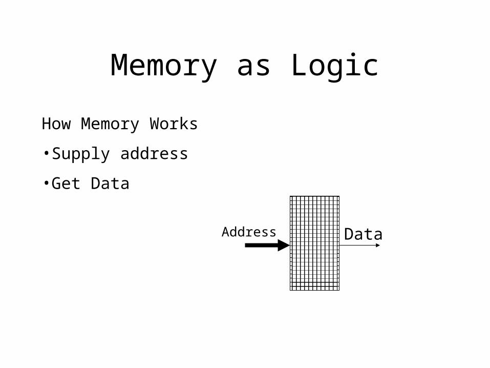
How Memory Works
•Supply address
•Get Data
Memory as Logic
Address Data
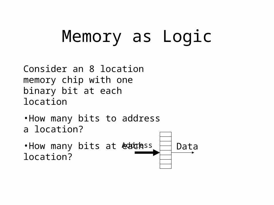
Consider an 8 location memory chip with one binary bit at each location
•How many bits to address a location?
•How many bits at each location?
Memory as Logic
Address Data
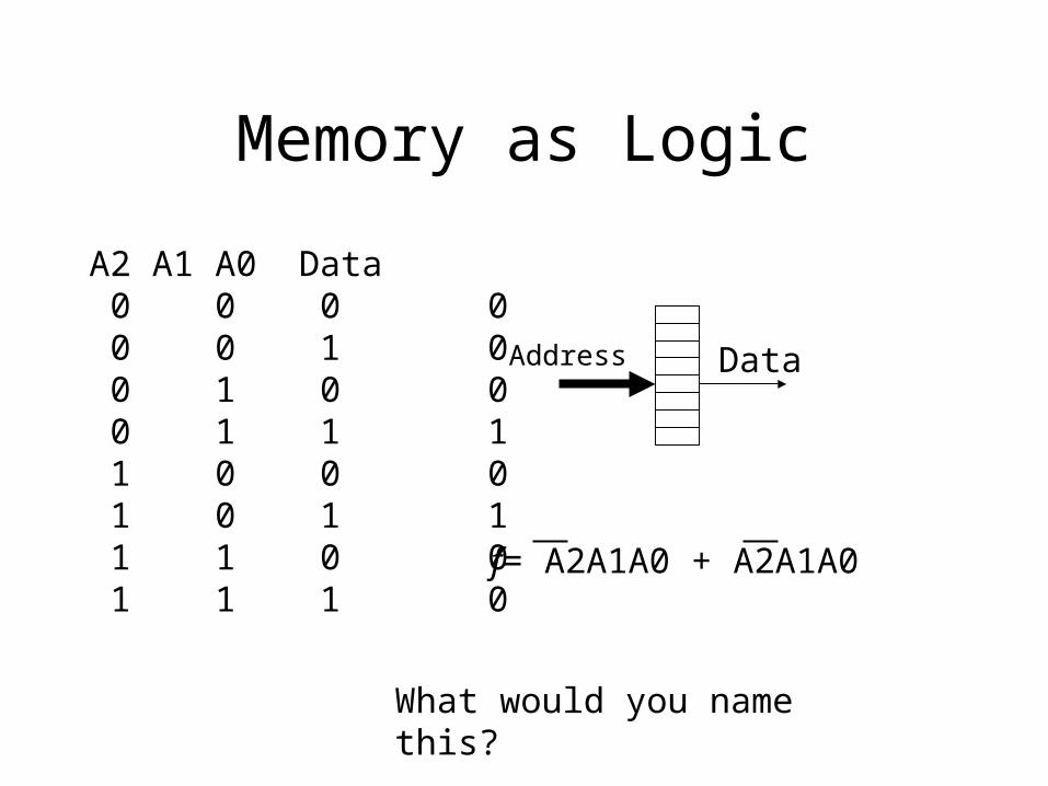
A2 A1 A0 Data 0 0 0 0 0 0 1 0 0 1 0 0 0 1 1 1 1 0 0 0 1 0 1 1 1 1 0 0 1 1 1 0
f= A2A1A0 + A2A1A0
What would you name this?
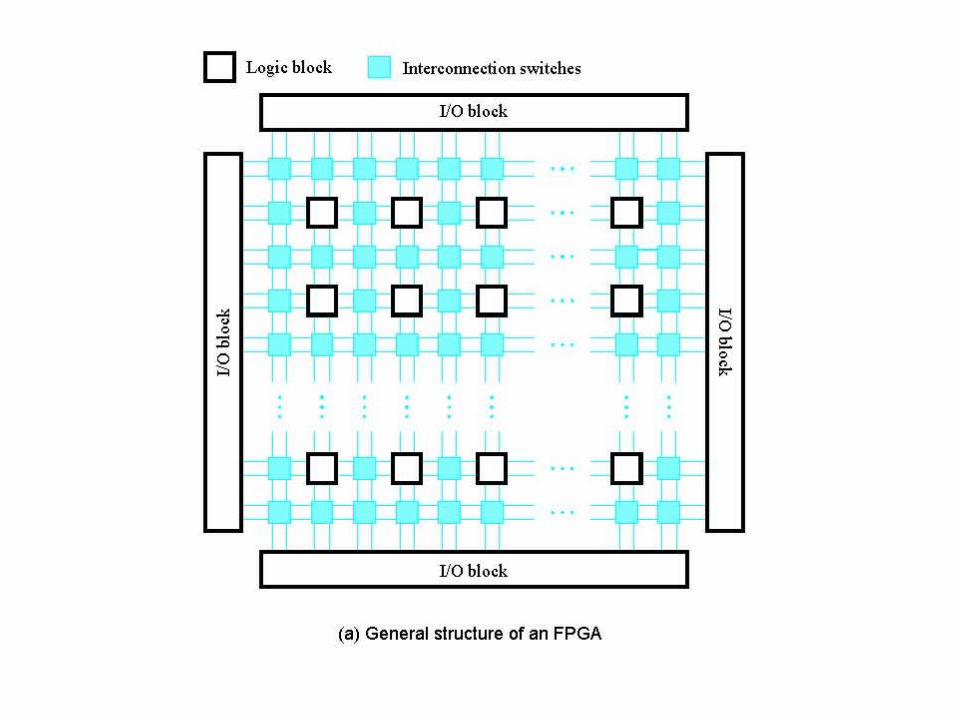
FPGA – Field Programmable Gate Arrays
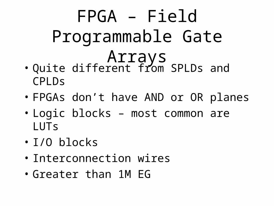
• Quite different from SPLDs and CPLDs
• FPGAs don’t have AND or OR planes
• Logic blocks – most common are LUTs
• I/O blocks
• Interconnection wires
• Greater than 1M EG
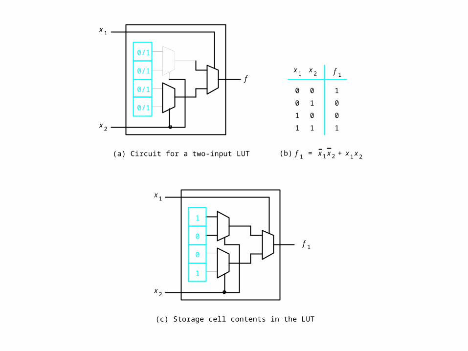
(a) Circuit for a two-input LUT
x 1
x 2
f
0/1
0/1
0/1
0/1
0
0
1
1
0
1
0
1
1
0
0
1
x 1 x 2
(b) f 1 x 1 x 2 x 1 x 2 + =
(c) Storage cell contents in the LUT
x 1
x 2
1
0
0
1
f 1
f 1
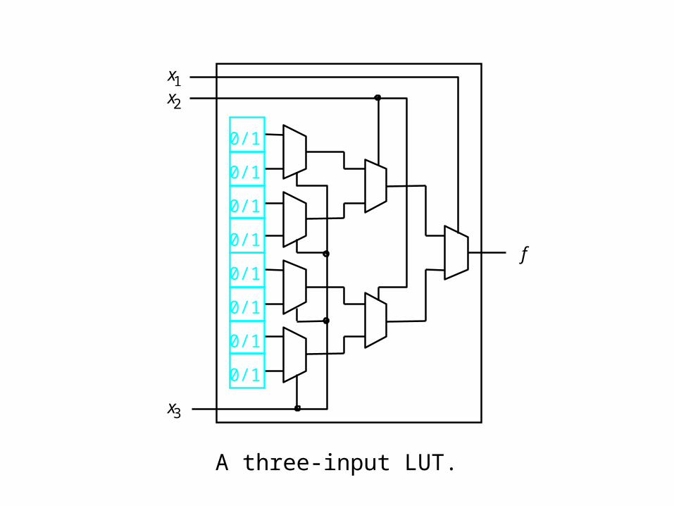
A three-input LUT.
f
0/1
0/1
0/1
0/1
0/1
0/1
0/1
0/1
x 2
x 3
x 1
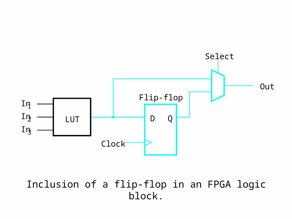
Inclusion of a flip-flop in an FPGA logic block.
Out
D Q
Clock
Select
Flip-flop In1
In2
In3
LUT
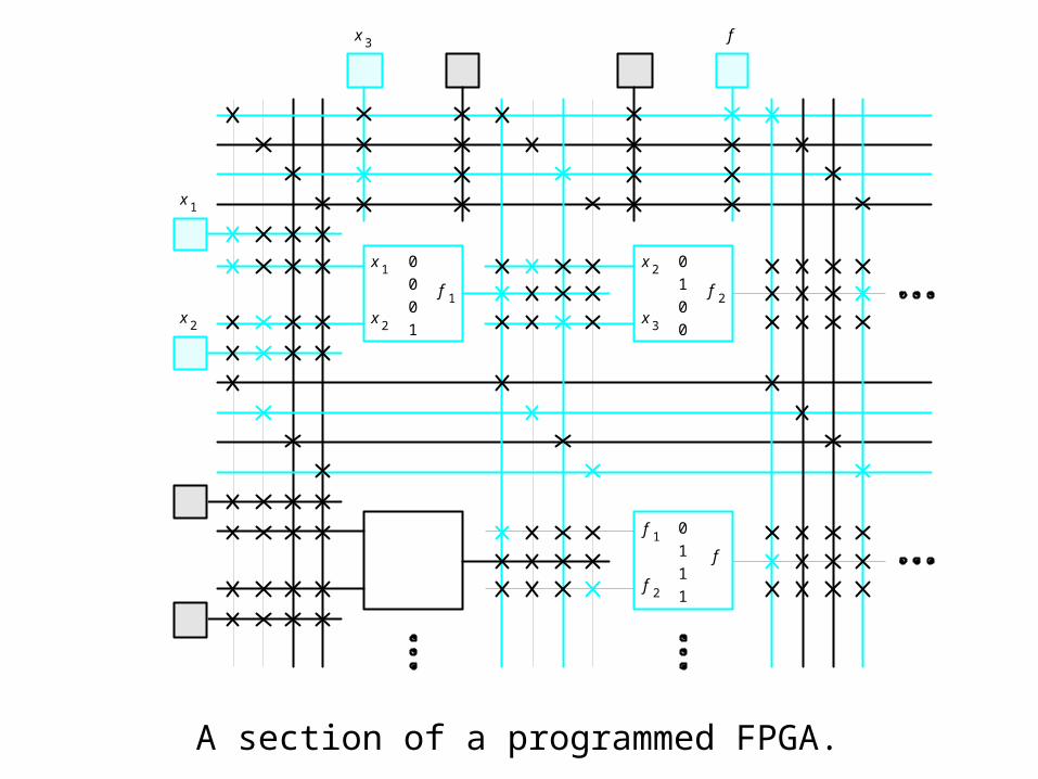
A section of a programmed FPGA.
0 1 0 0
0 1 1 1
0 0 0 1
x 1
x 2
x 2
x 3
f 1
f 2
f 1 f 2
f
x 1
x 2
x 3 f
Custom Chips, Standard Cells, & Gate Arrays
• Programmable switches– Size issue– Speed issue
Custom Chips
• Complete flexibility in transistor placement and connection
• Large design effort
• Large cost
• Large quantities
ASICsApplication Specific Integrated Circuits
• Standard Cell Libraries
• Configurable connections
Gate Arrays
• Gates prefabricated
• Connections added later
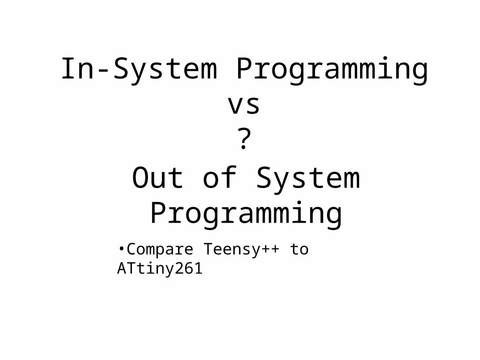
In-System Programmingvs?
•Compare Teensy++ to ATtiny261
Out of System Programming
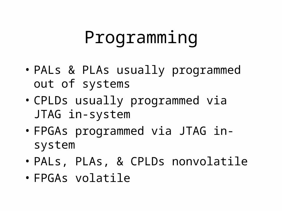
Programming
• PALs & PLAs usually programmed out of systems
• CPLDs usually programmed via JTAG in-system
• FPGAs programmed via JTAG in-system
• PALs, PLAs, & CPLDs nonvolatile
• FPGAs volatile
Practical Aspects
• Transistor Operation
• Static Operation - Voltage Levels
• Dynamic Operation – Transition Times
• Power Dissipation
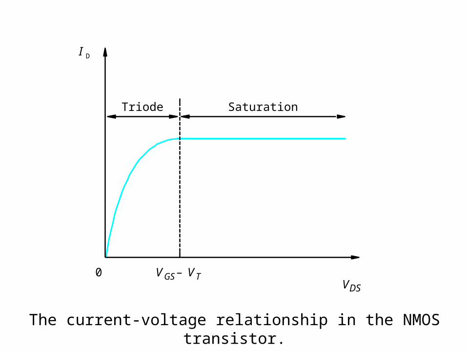
0
Triode
V DS
Saturation
V GS V T –
I D
The current-voltage relationship in the NMOS transistor.
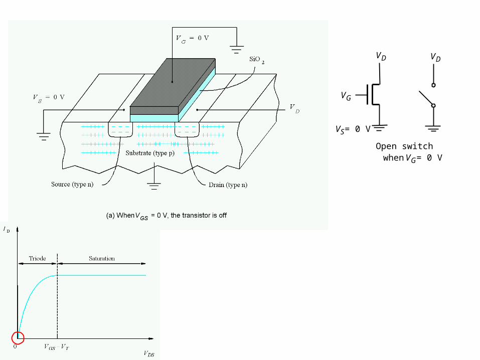
V G
V D
V S = 0 V
Open switch whenV G = 0 V
V D
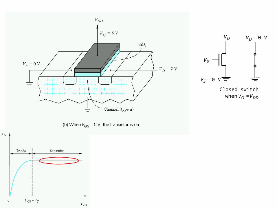
V G
V D
V S = 0 V
Closed switch whenV G =V DD
V D = 0 V
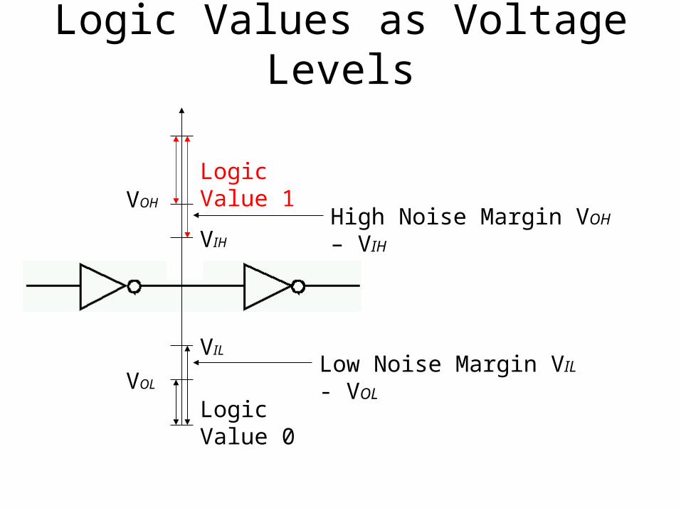
Logic Values as Voltage Levels
VOH
VOL
VIH
VIL
Logic Value 0
Logic Value 1
High Noise Margin VOH – VIH
Low Noise Margin VIL - VOL
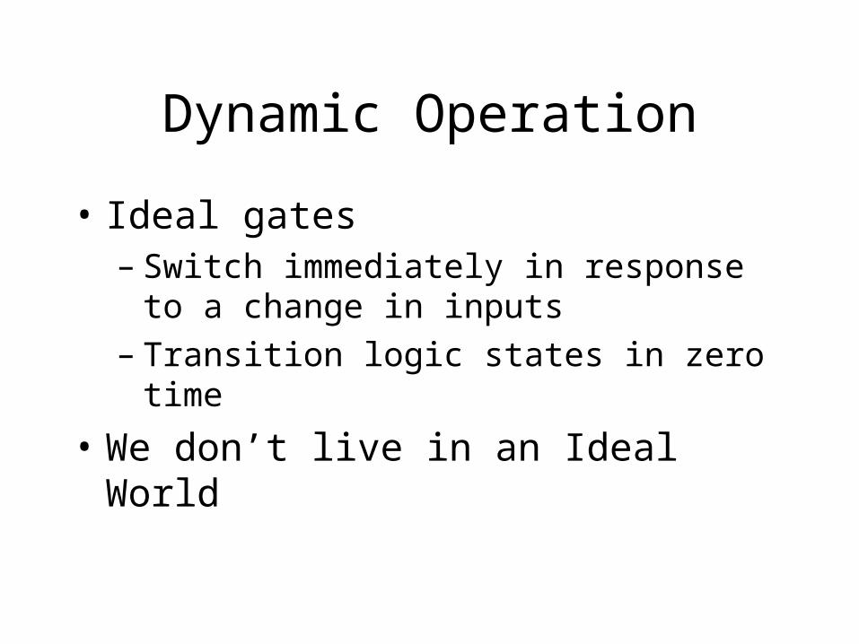
Dynamic Operation
• Ideal gates – Switch immediately in response to a change in
inputs– Transition logic states in zero time
• We don’t live in an Ideal World
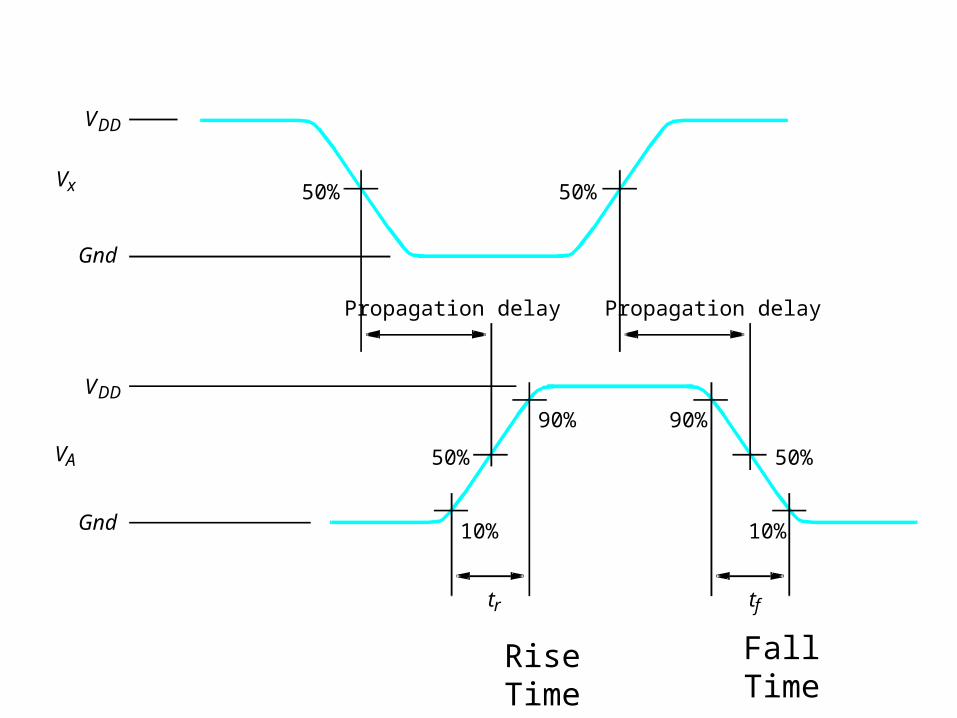
Propagation delay
V DD
V DD
Gnd
Gnd
V x
V A
50% 50%
90%
Propagation delay
10%
t r
50%
90%
50%
10%
t f
Rise Time Fall Time
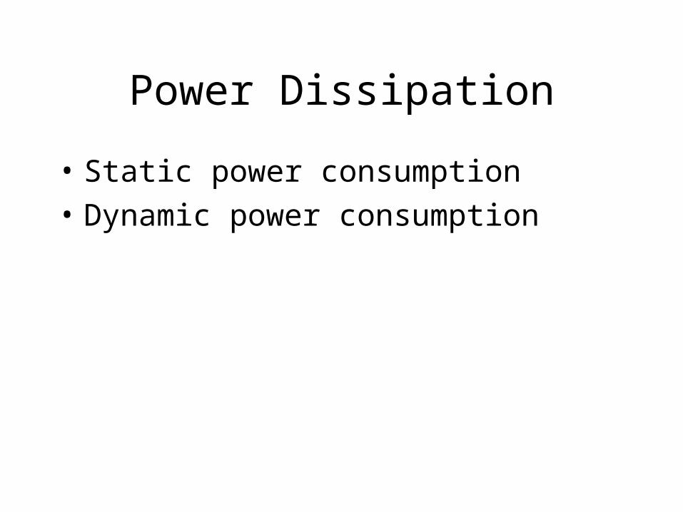
Power Dissipation
• Static power consumption
• Dynamic power consumption
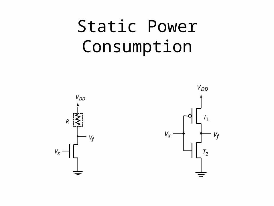
Static Power Consumption
V x
V f
V DD
R
V f
V DD
V x
T 1
T 2
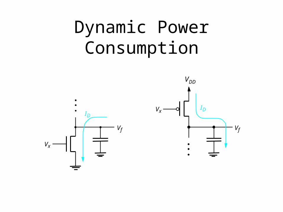
Dynamic Power Consumption
VDD
Vf
Vx
IDVx
Vf
ID
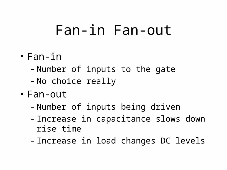
Fan-in Fan-out
• Fan-in– Number of inputs to the gate– No choice really
• Fan-out– Number of inputs being driven– Increase in capacitance slows down rise time– Increase in load changes DC levels
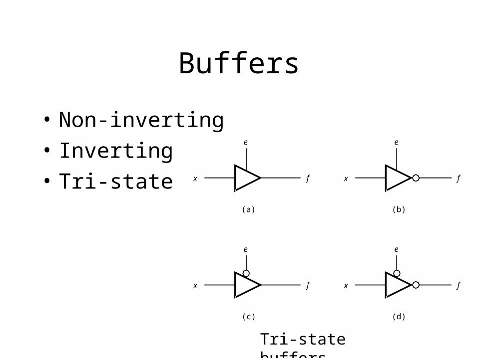
Buffers
• Non-inverting
• Inverting
• Tri-state x f
e
(b)
x f
e
(a)
x f
e
(c)
x f
e
(d)
Tri-state buffers
Reading• Chapter 3
Laboratory Preparation• None
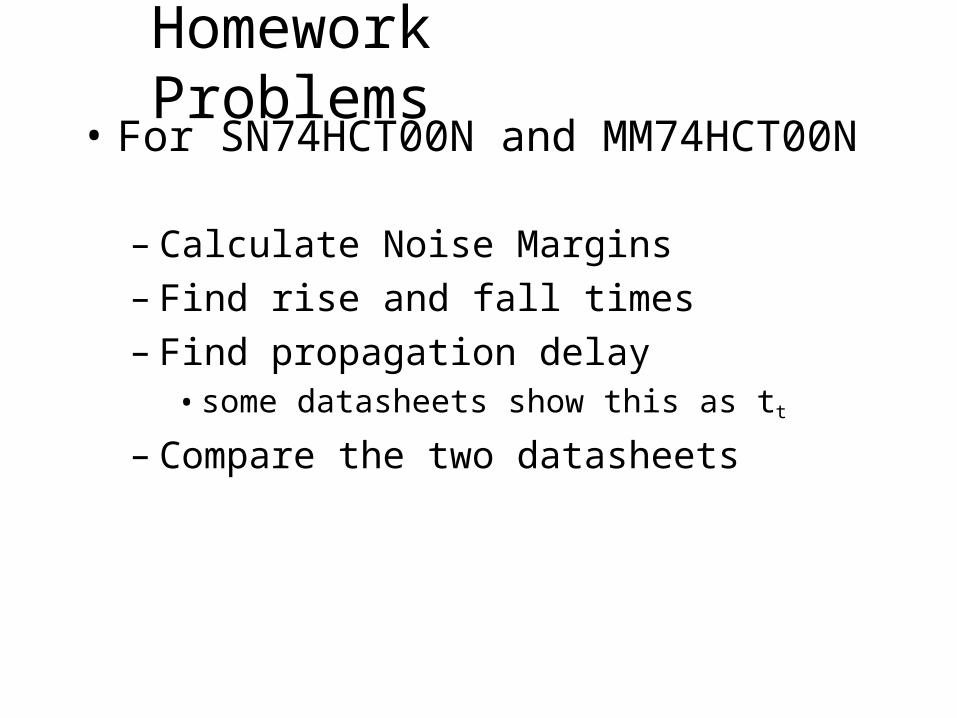
Homework Problems• For SN74HCT00N and MM74HCT00N
– Calculate Noise Margins– Find rise and fall times– Find propagation delay
• some datasheets show this as tt
– Compare the two datasheets
![Gates and Logic: From Transistors to Logic Gates and Logic ......Gates and Logic: From Transistors to Logic Gates and Logic Circuits [Weatherspoon, Bala, Bracy, and Sirer] Prof. Hakim](https://static.fdocuments.us/doc/165x107/5fa95cb6eb1af8231472f381/gates-and-logic-from-transistors-to-logic-gates-and-logic-gates-and-logic.jpg)