Chapter 3: Combinational Logic Design - Anadolu University 232/icerik/Week 4 Combinatio… ·...
45
1 Chapter 3: Combinational Logic Design
Transcript of Chapter 3: Combinational Logic Design - Anadolu University 232/icerik/Week 4 Combinatio… ·...
1
Chapter 3: Combinational Logic Design
2
Introduction
• We have learned all the prerequisite material:– Truth tables and Boolean expressions describe functions– Expressions can be converted into hardware circuits– Boolean algebra and K-maps help simplify expressions and circuits
• Now, let us put all of these foundations to good use, to analyze and designsome larger circuits
3
Introduction
• Logic circuits for digital systems may be
– Combinational– Sequential
• A combinational circuit consists of logic gates whose outputs at any time are determined by the current input values, i.e., it has no memory elements
• A sequential circuit consists of logic gates whose outputs at any time are determined by the current input values as well as the past input values, i.e., it has memory elements
4
Introduction
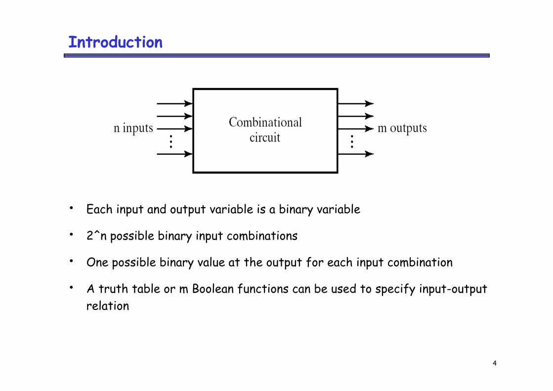
• Each input and output variable is a binary variable
• 2^n possible binary input combinations
• One possible binary value at the output for each input combination
• A truth table or m Boolean functions can be used to specify input-outputrelation
5
Design Hierarchy
• A single very large-scale integrated (VLSI) processos circuit containsseveral tens of millions of gates!
• Imagine interconnecting these gates to form the processor
• No complex circuit can be designed simply by interconnecting gatesone at a time
• Divide and Conquer approach is used to deal with the complexity
– Break up the circuit into pieces (blocks)– Define the functions and the interfaces of each block such that the
circuit formed by interconnecting the blocks obeys the original circuit specification
– If a block is still too large and complex to be designed as a singleentity, it can be broken into smaller blocks
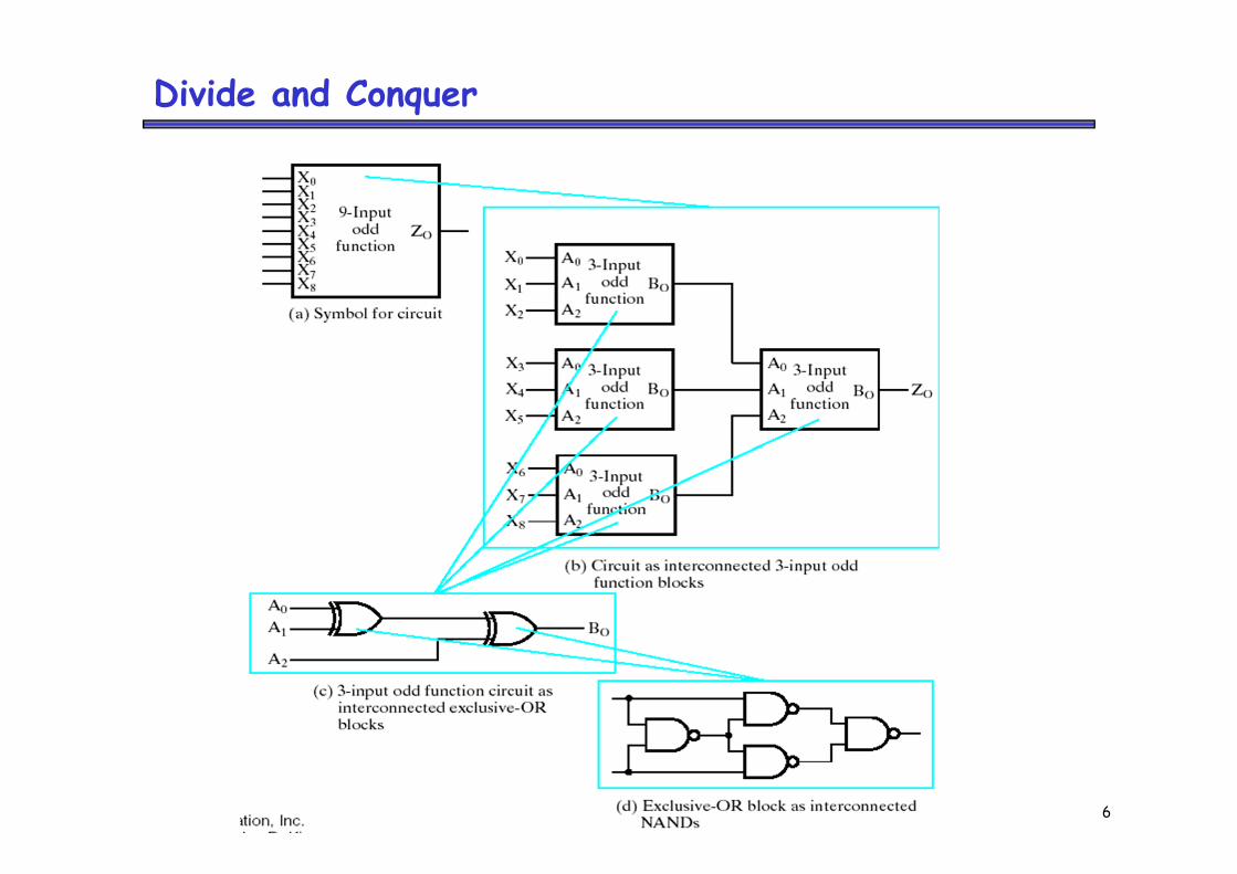
6
Divide and Conquer
7
Hierarchical Design due to Divide and Conquer
8
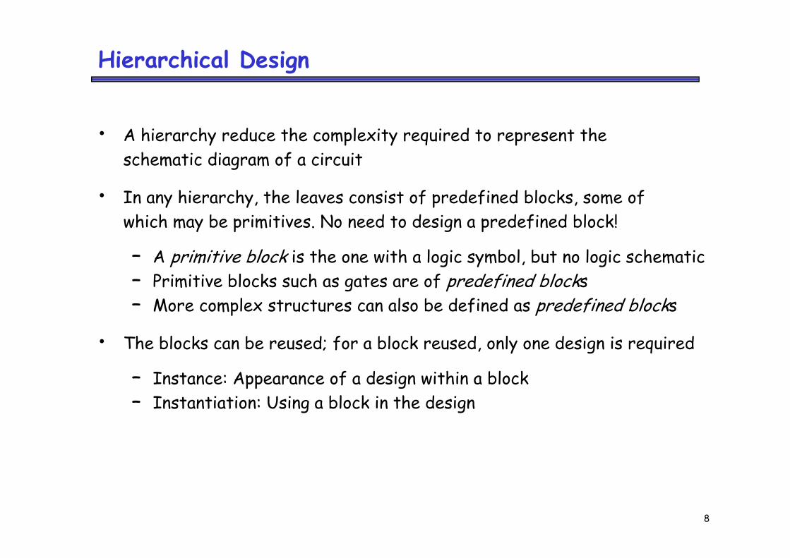
Hierarchical Design
• A hierarchy reduce the complexity required to represent the schematic diagram of a circuit
• In any hierarchy, the leaves consist of predefined blocks, some of which may be primitives. No need to design a predefined block!
– A primitive block is the one with a logic symbol, but no logic schematic– Primitive blocks such as gates are of predefined blocks– More complex structures can also be defined as predefined blocks
• The blocks can be reused; for a block reused, only one design is required
– Instance: Appearance of a design within a block– Instantiation: Using a block in the design
9
Designing Complex Circuits
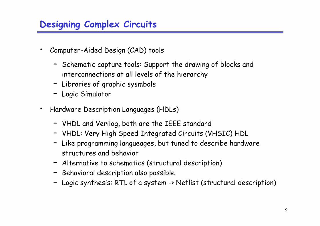
• Computer-Aided Design (CAD) tools
– Schematic capture tools: Support the drawing of blocks and interconnections at all levels of the hierarchy
– Libraries of graphic sysmbols– Logic Simulator
• Hardware Description Languages (HDLs)
– VHDL and Verilog, both are the IEEE standard– VHDL: Very High Speed Integrated Circuits (VHSIC) HDL– Like programming langueages, but tuned to describe hardware
structures and behavior– Alternative to schematics (structural description)– Behavioral description also possible– Logic synthesis: RTL of a system -> Netlist (structural description)
10
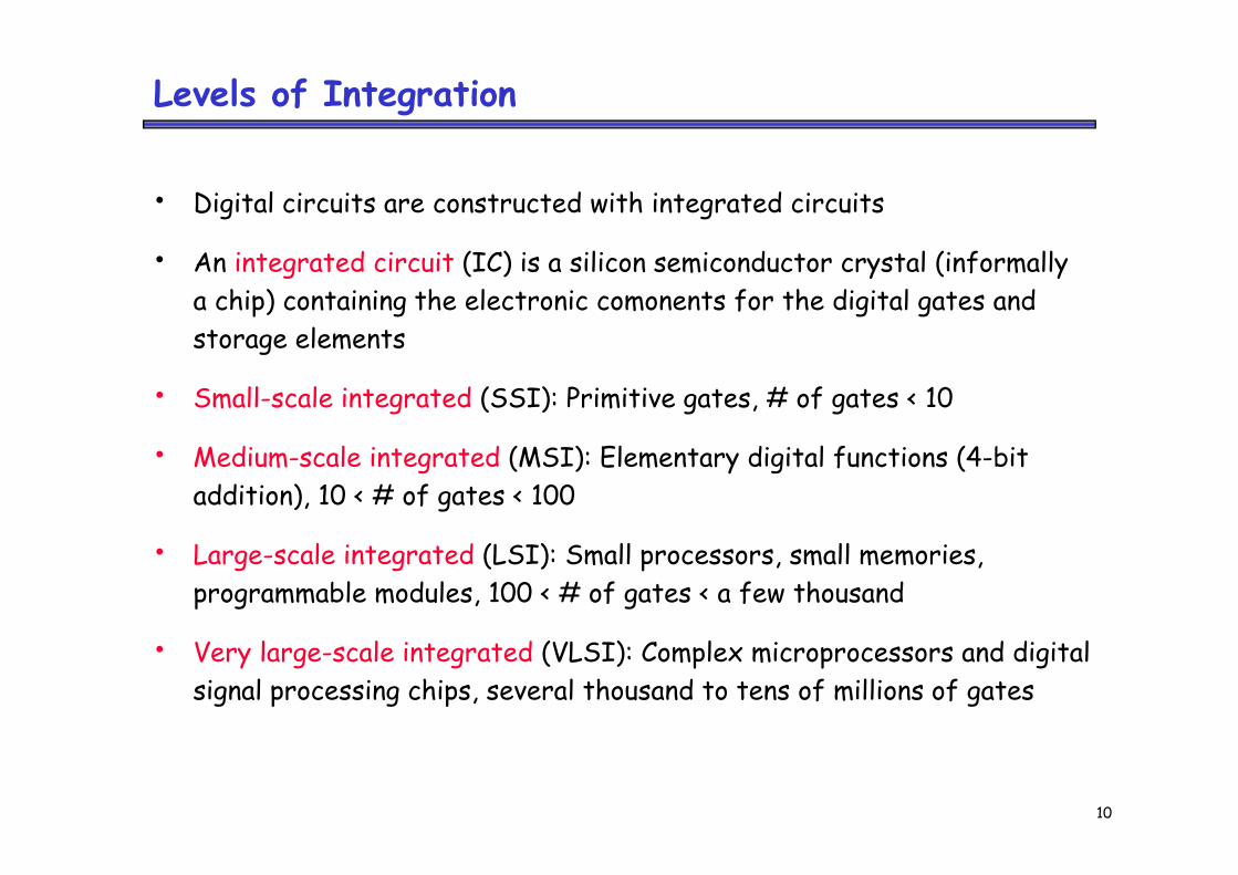
Levels of Integration
• Digital circuits are constructed with integrated circuits
• An integrated circuit (IC) is a silicon semiconductor crystal (informallya chip) containing the electronic comonents for the digital gates andstorage elements
• Small-scale integrated (SSI): Primitive gates, # of gates < 10
• Medium-scale integrated (MSI): Elementary digital functions (4-bit addition), 10 < # of gates < 100
• Large-scale integrated (LSI): Small processors, small memories, programmable modules, 100 < # of gates < a few thousand
• Very large-scale integrated (VLSI): Complex microprocessors and digitalsignal processing chips, several thousand to tens of millions of gates
11
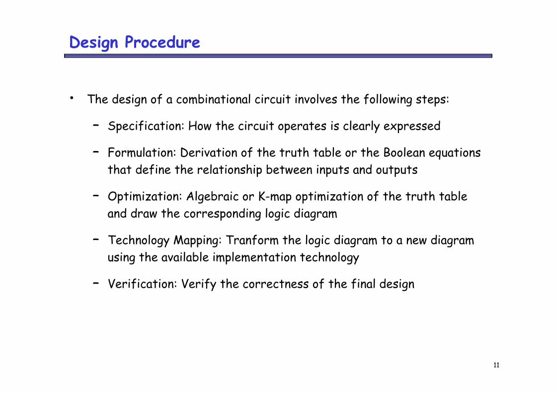
Design Procedure
• The design of a combinational circuit involves the following steps:
– Specification: How the circuit operates is clearly expressed
– Formulation: Derivation of the truth table or the Boolean equationsthat define the relationship between inputs and outputs
– Optimization: Algebraic or K-map optimization of the truth tableand draw the corresponding logic diagram
– Technology Mapping: Tranform the logic diagram to a new diagramusing the available implementation technology
– Verification: Verify the correctness of the final design
12
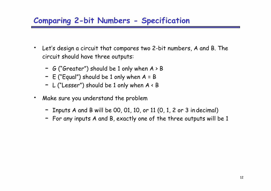
Comparing 2-bit Numbers - Specification
• Let’s design a circuit that compares two 2-bit numbers, A and B. The circuit should have three outputs:
– G (“Greater”) should be 1 only when A > B– E (“Equal”) should be 1 only when A = B– L (“Lesser”) should be 1 only when A < B
• Make sure you understand the problem
– Inputs A and B will be 00, 01, 10, or 11 (0, 1, 2 or 3 indecimal)– For any inputs A and B, exactly one of the three outputs will be 1
13
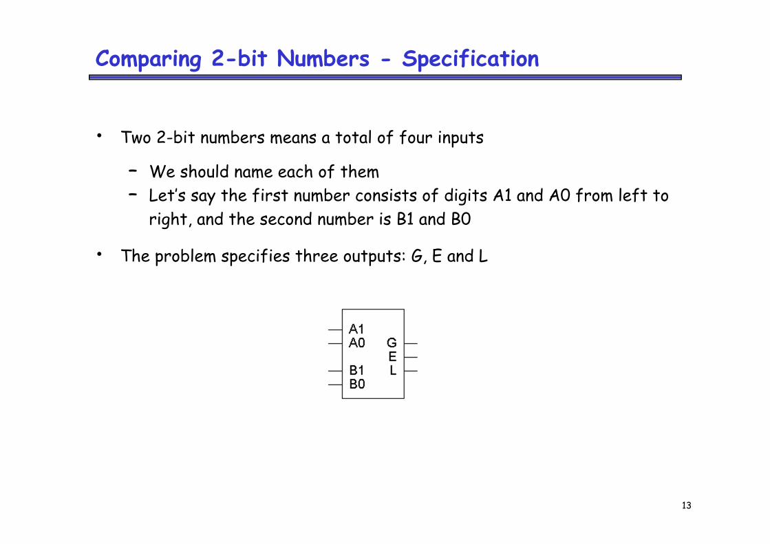
• Two 2-bit numbers means a total of four inputs
– We should name each of them– Let’s say the first number consists of digits A1 and A0 from left to
right, and the second number is B1 and B0
• The problem specifies three outputs: G, E and L
Comparing 2-bit Numbers - Specification
14
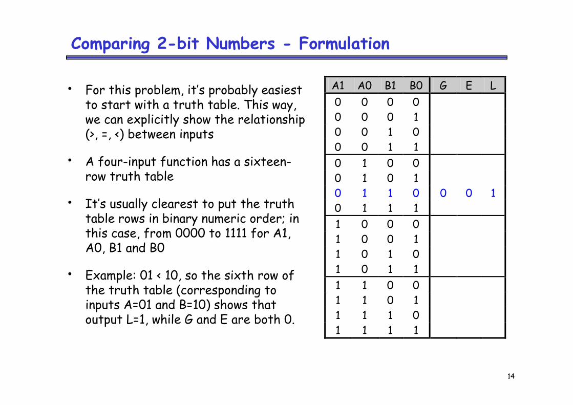
Comparing 2-bit Numbers - Formulation
• For this problem, it’s probably easiest to start with a truth table. This way, we can explicitly show the relationship (>, =, <) between inputs
• A four-input function has a sixteen-row truth table
• It’s usually clearest to put the truth table rows in binary numeric order; in this case, from 0000 to 1111 for A1, A0, B1 and B0
• Example: 01 < 10, so the sixth row of the truth table (corresponding to inputs A=01 and B=10) shows that output L=1, while G and E are both 0.
A1 A0 B1 B0 G E L 0 0 0 0 0 0 0 1 0 0 1 0 0 0 1 1 0 1 0 0 0 1 0 1 0 1 1 0 0 0 1 0 1 1 1 1 0 0 0 1 0 0 1 1 0 1 0 1 0 1 1 1 1 0 0 1 1 0 1 1 1 1 0 1 1 1 1
15
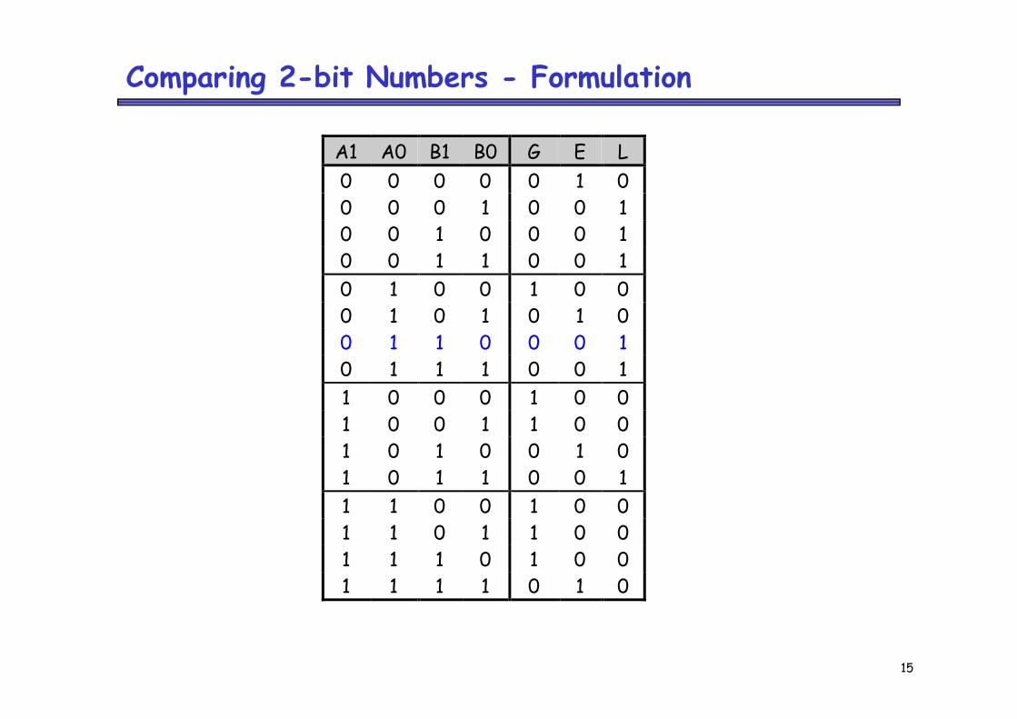
A1 A0 B1 B0 G E L0 0 0 0 0 1 00 0 0 1 0 0 10 0 1 0 0 0 10 0 1 1 0 0 10 1 0 0 1 0 00 1 0 1 0 1 00 1 1 0 0 0 10 1 1 1 0 0 11 0 0 0 1 0 01 0 0 1 1 0 01 0 1 0 0 1 01 0 1 1 0 0 11 1 0 0 1 0 01 1 0 1 1 0 01 1 1 0 1 0 01 1 1 1 0 1 0
Comparing 2-bit Numbers - Formulation
16
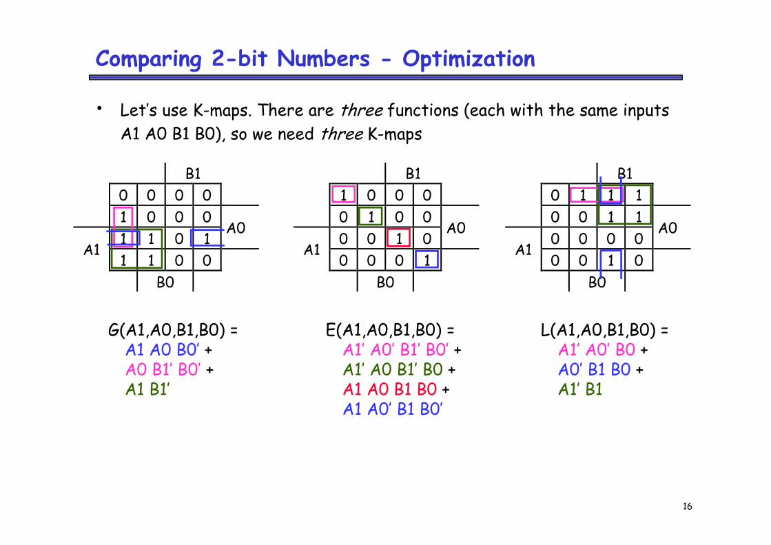
• Let’s use K-maps. There are three functions (each with the same inputs A1 A0 B1 B0), so we need three K-maps
G(A1,A0,B1,B0) =A1 A0 B0’ + A0 B1’ B0’ + A1 B1’
E(A1,A0,B1,B0) =A1’ A0’ B1’ B0’ +A1’ A0 B1’ B0 +A1 A0 B1 B0 +A1 A0’ B1 B0’
L(A1,A0,B1,B0) =A1’ A0’ B0 + A0’ B1 B0 +A1’ B1
B10 0 0 01 0 0 01 1 0 1
A0A1
1 1 0 0B0
B11 0 0 00 1 0 00 0 1 0
A0A1
0 0 0 1B0
B10 1 1 10 0 1 10 0 0 0
A0A1
0 0 1 0B0
Comparing 2-bit Numbers - Optimization
17
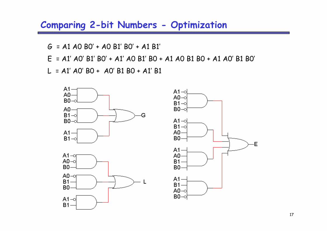
Comparing 2-bit Numbers - Optimization
G = A1 A0 B0’ + A0 B1’ B0’ + A1 B1’E = A1’ A0’ B1’ B0’ + A1’ A0 B1’ B0 + A1 A0 B1 B0 + A1 A0’ B1 B0’L = A1’ A0’ B0 + A0’ B1 B0 + A1’ B1
18
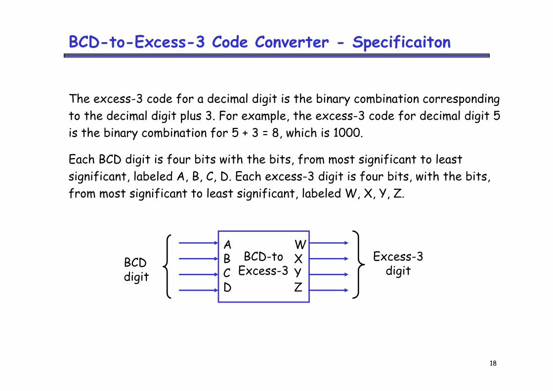
BCD-to-Excess-3 Code Converter - Specificaiton
The excess-3 code for a decimal digit is the binary combination correspondingto the decimal digit plus 3. For example, the excess-3 code for decimal digit 5is the binary combination for 5 + 3 = 8, which is 1000.
Each BCD digit is four bits with the bits, from most significant to leastsignificant, labeled A, B, C, D. Each excess-3 digit is four bits, with the bits,from most significant to least significant, labeled W, X, Y, Z.
ABCD
WXYZ
BCDdigit
Excess-3digit
BCD-toExcess-3
19
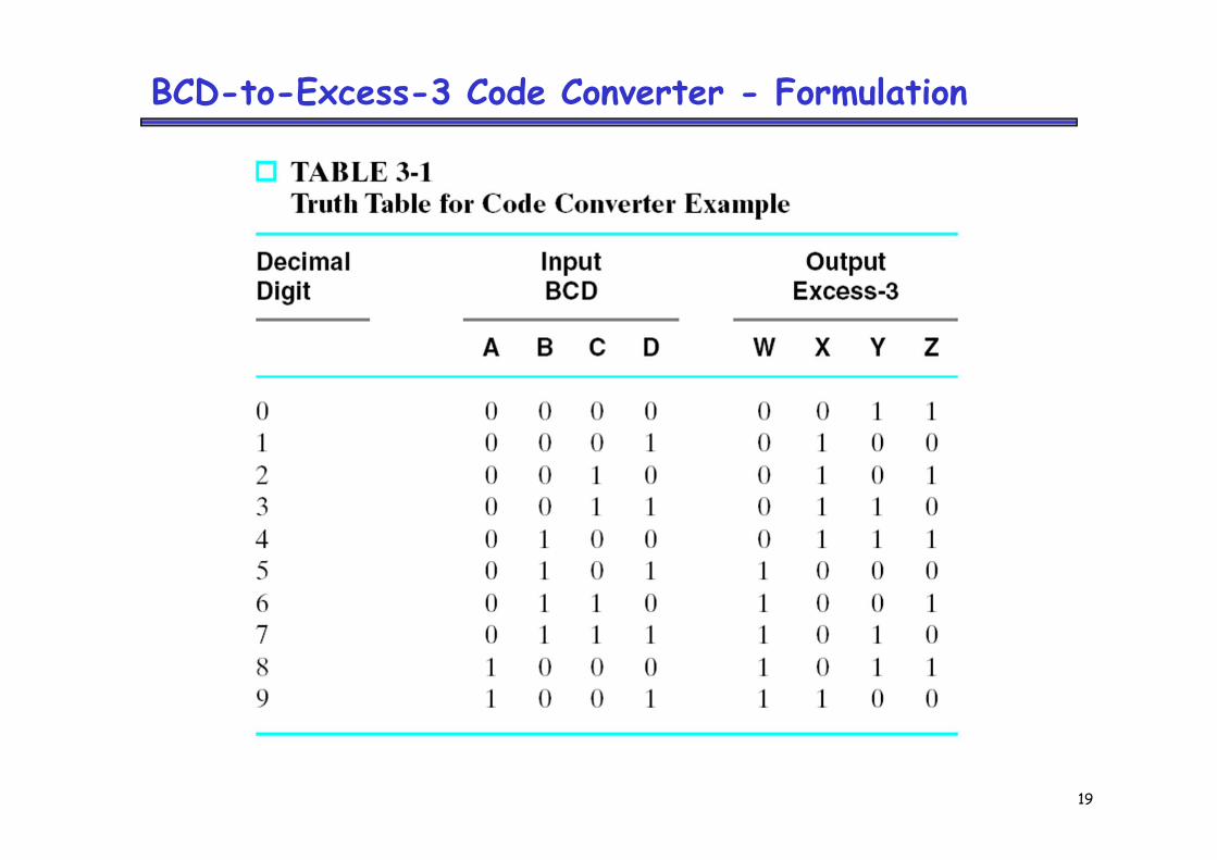
BCD-to-Excess-3 Code Converter - Formulation
20
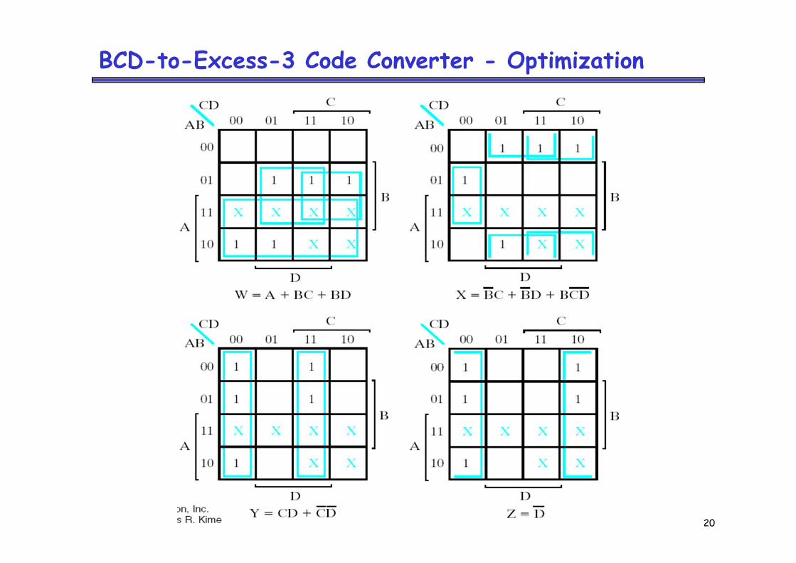
BCD-to-Excess-3 Code Converter - Optimization
21
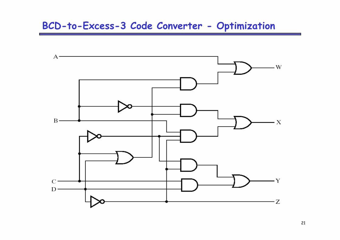
BCD-to-Excess-3 Code Converter - Optimization
22
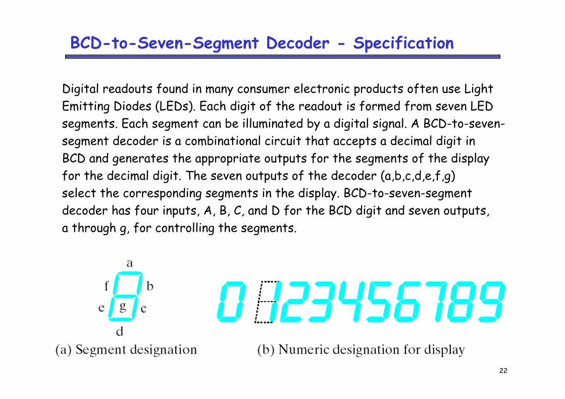
BCD-to-Seven-Segment Decoder - Specification
Digital readouts found in many consumer electronic products often use LightEmitting Diodes (LEDs). Each digit of the readout is formed from seven LEDsegments. Each segment can be illuminated by a digital signal. A BCD-to-seven-segment decoder is a combinational circuit that accepts a decimal digit inBCD and generates the appropriate outputs for the segments of the displayfor the decimal digit. The seven outputs of the decoder (a,b,c,d,e,f,g)select the corresponding segments in the display. BCD-to-seven-segmentdecoder has four inputs, A, B, C, and D for the BCD digit and seven outputs,a through g, for controlling the segments.
23
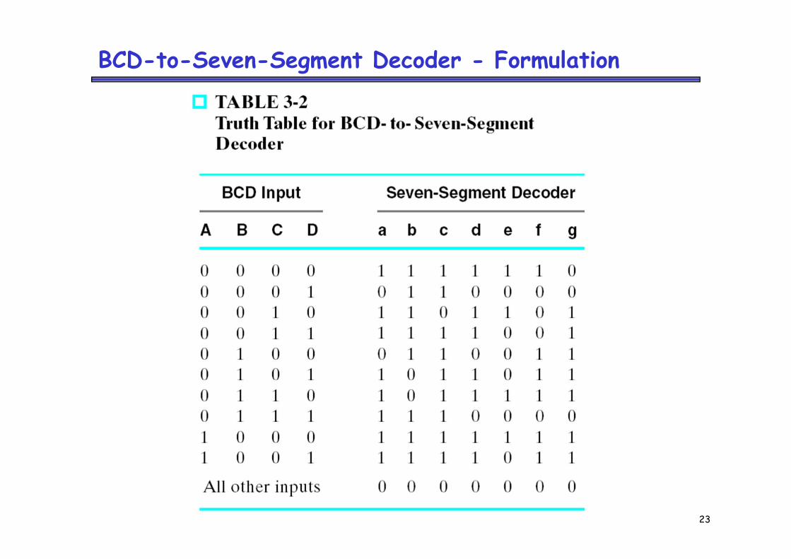
BCD-to-Seven-Segment Decoder - Formulation
24
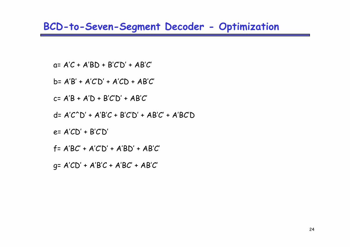
BCD-to-Seven-Segment Decoder - Optimization
a= A’C + A’BD + B’C’D’ + AB’C’
b= A’B’ + A’C’D’ + A’CD + AB’C’
c= A’B + A’D + B’C’D’ + AB’C’
d= A’C^D’ + A’B’C + B’C’D’ + AB’C’ + A’BC’D
e= A’CD’ + B’C’D’
f= A’BC’ + A’C’D’ + A’BD’ + AB’C’
g= A’CD’ + A’B’C + A’BC’ + AB’C’
25
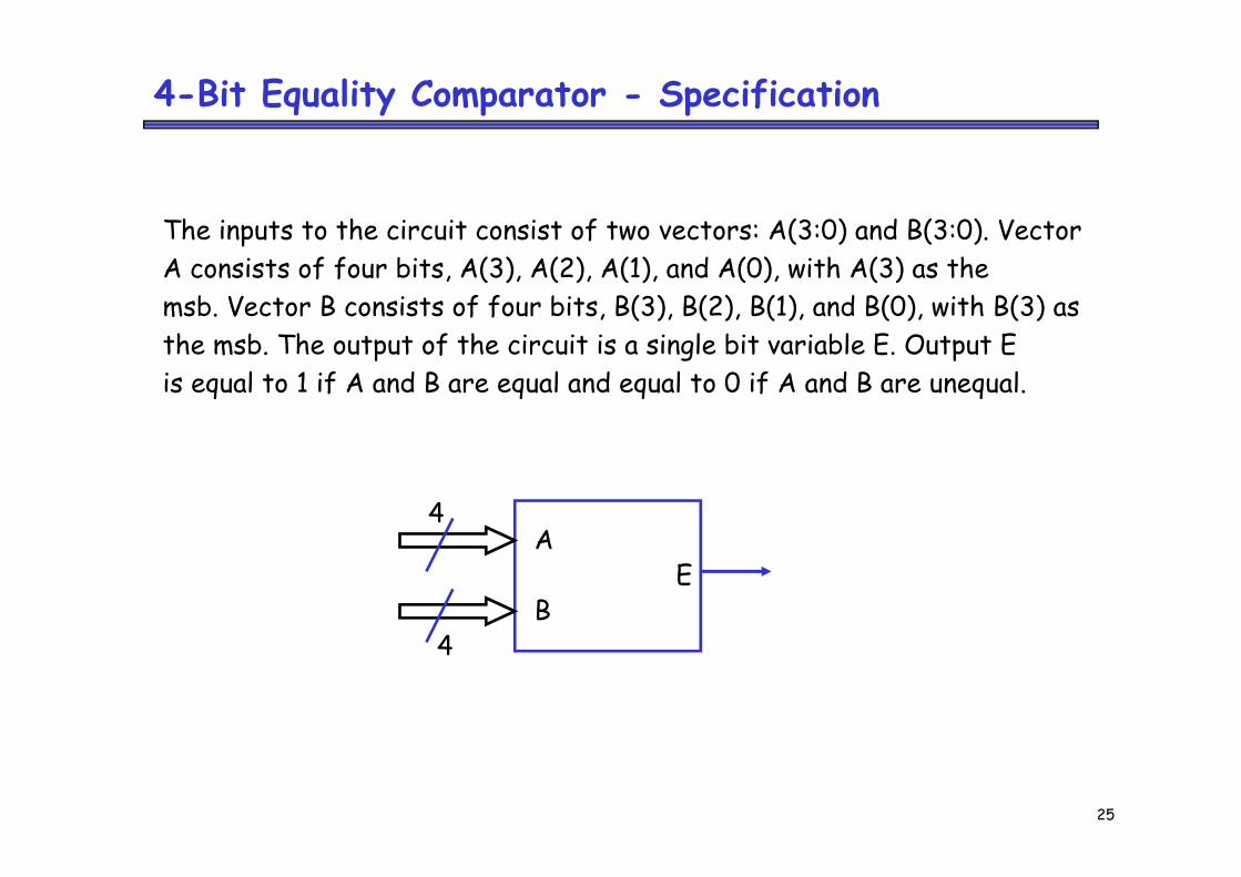
4-Bit Equality Comparator - Specification
The inputs to the circuit consist of two vectors: A(3:0) and B(3:0). VectorA consists of four bits, A(3), A(2), A(1), and A(0), with A(3) as themsb. Vector B consists of four bits, B(3), B(2), B(1), and B(0), with B(3) as the msb. The output of the circuit is a single bit variable E. Output Eis equal to 1 if A and B are equal and equal to 0 if A and B are unequal.
4
4
A
BE
26
4-Bit Equality Comparator - Formulation
• Since there are 8 inputs, using a truth table is impractical!!!
• Apply divide and conquer design approach
• Observation: In order for A and B to be equal, the bit values in each ofthe respective positions, 3 down to 0, must be equal
• We need four 1-bit comparator
• We need an additional circuit to combine the outputs of 1-bit comparators
27
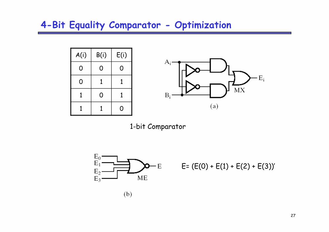
4-Bit Equality Comparator - Optimization
A(i) B(i) E(i)
0 0 0
0 1 1
1 0 1
1 1 0
1-bit Comparator
E= (E(0) + E(1) + E(2) + E(3))’
28
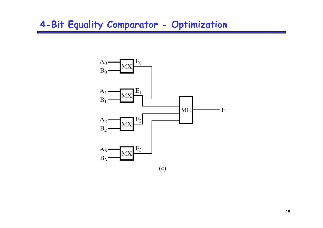
4-Bit Equality Comparator - Optimization
29
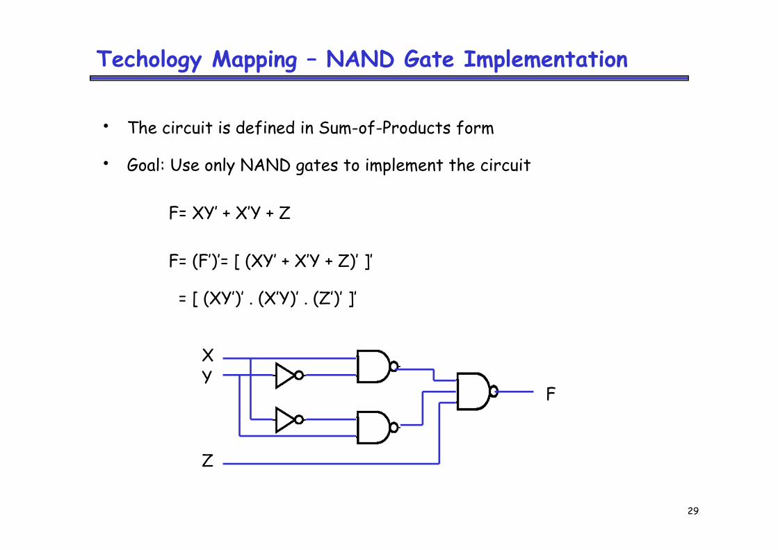
Techology Mapping – NAND Gate Implementation
• The circuit is defined in Sum-of-Products form
• Goal: Use only NAND gates to implement the circuit
F= XY’ + X’Y + Z
F= (F’)’= [ (XY’ + X’Y + Z)’ ]’
= [ (XY’)’ . (X’Y)’ . (Z’)’ ]’
XY
Z
F
30
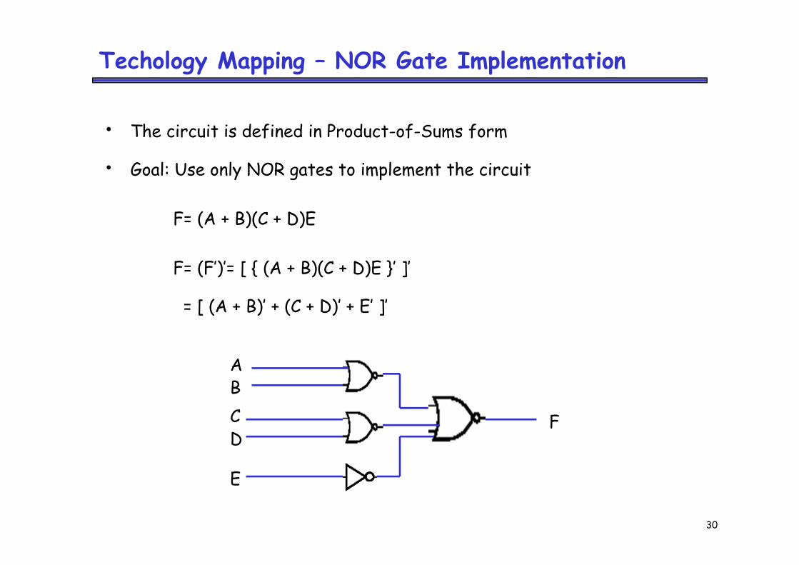
Techology Mapping – NOR Gate Implementation
• The circuit is defined in Product-of-Sums form
• Goal: Use only NOR gates to implement the circuit
F= (A + B)(C + D)E
F= (F’)’= [ { (A + B)(C + D)E }’ ]’
= [ (A + B)’ + (C + D)’ + E’ ]’
AB
FCD
E
31
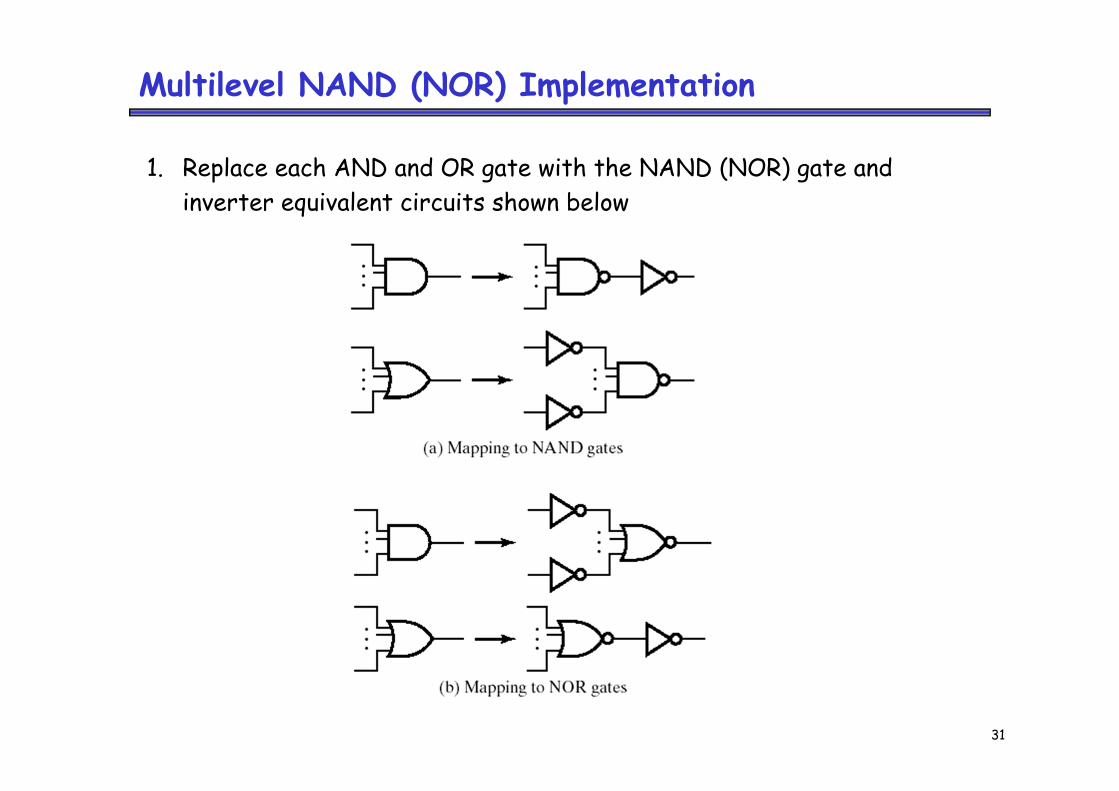
Multilevel NAND (NOR) Implementation
1. Replace each AND and OR gate with the NAND (NOR) gate and inverter equivalent circuits shown below
32
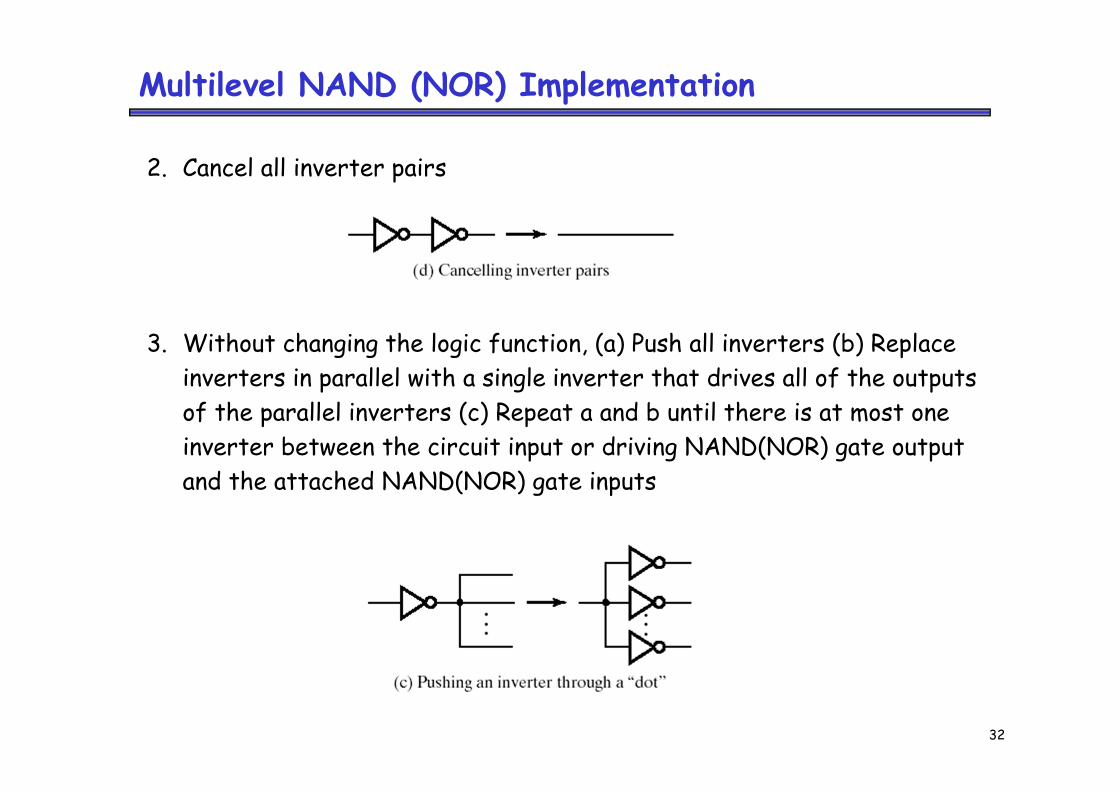
Multilevel NAND (NOR) Implementation
2. Cancel all inverter pairs
3. Without changing the logic function, (a) Push all inverters (b) Replaceinverters in parallel with a single inverter that drives all of the outputsof the parallel inverters (c) Repeat a and b until there is at most oneinverter between the circuit input or driving NAND(NOR) gate outputand the attached NAND(NOR) gate inputs
33
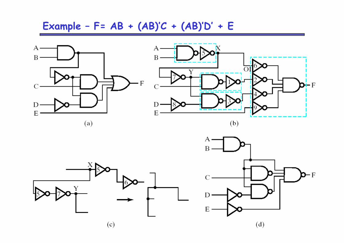
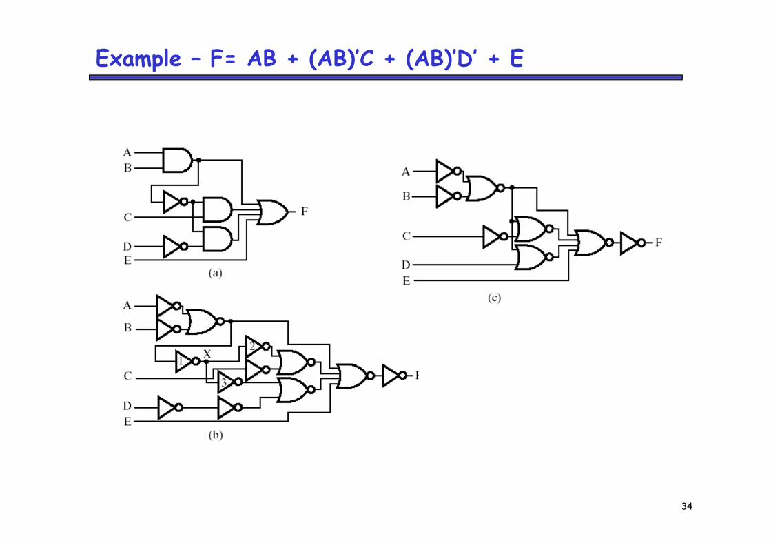
Example – F= AB + (AB)’C + (AB)’D’ + E
34
Example – F= AB + (AB)’C + (AB)’D’ + E
35
Summary
• Functions can be represented with expressions, truth tables or circuits. These are all equivalent, and we can arbitrarily transform between them
• Designing a circuit requires you to first find a (simplified) Boolean expression for the functionyou want to compute. You can then convert the expression into a circuit
36
Summary
• NAND and NOR are universal gates which can replace all others
– There are two representations for NAND gates (AND-NOT and NOT-OR), which are equivalent by DeMorgan’s law
– Similarly, there are two representations for NOR gates too
• You can convert a circuit with primitive gates into a NAND or NOR diagramby judicious use of the axiom (x’)’ = x, to ensure that you don’t change theoverall function
37
Summary
• Circuits made up of gates, that don’t have any feedback, are called combinatorial circuits
– No feedback: outputs are not connected to inputs– If you change the inputs, and wait for a while, the correct outputs show
up• Why? Capacitive loading (“fill up the water level” analogy)
• So, when such ckts are used in a computer, the time it takes to get stable outputs is important
• For the same reason, a single output cannot drive too many inputs
– Will be too slow to “fill them up”– May not have enough power
• So, the design criteria are:
– Propagation delay (how many gets in a sequence from in to out)– Fan-out– Fan-in (Number of inputs to a single gate)
38
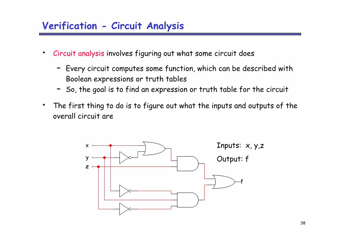
Verification - Circuit Analysis
• Circuit analysis involves figuring out what some circuit does
– Every circuit computes some function, which can be described with Boolean expressions or truth tables
– So, the goal is to find an expression or truth table for the circuit
• The first thing to do is to figure out what the inputs and outputs of the overall circuit are
Inputs: x, y,z
Output: f
39
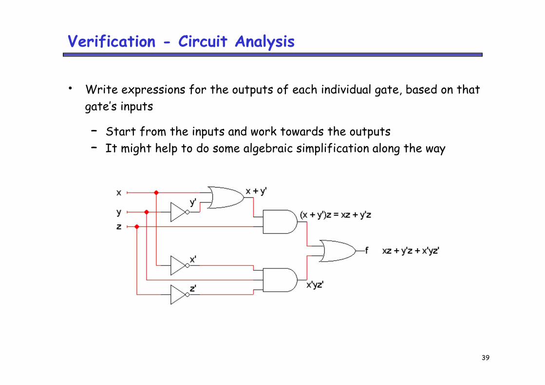
• Write expressions for the outputs of each individual gate, based on that gate’s inputs
– Start from the inputs and work towards the outputs– It might help to do some algebraic simplification along the way
Verification - Circuit Analysis
40
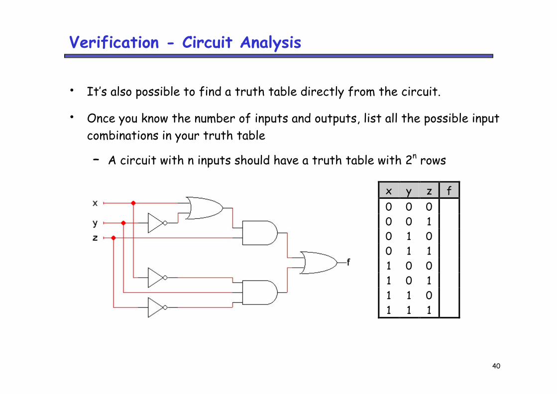
Verification - Circuit Analysis
• It’s also possible to find a truth table directly from the circuit.
• Once you know the number of inputs and outputs, list all the possible input combinations in your truth table
– A circuit with n inputs should have a truth table with 2n rows
x y z f0 0 00 0 10 1 00 1 11 0 01 0 11 1 01 1 1
41
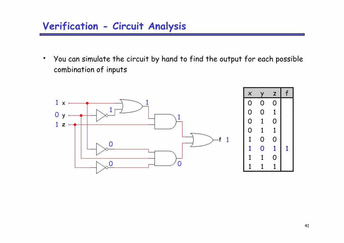
Verification - Circuit Analysis
• You can simulate the circuit by hand to find the output for each possiblecombination of inputs
x y z f0 0 00 0 10 1 00 1 11 0 01 0 1 11 1 01 1 1
1
01
1
0
0
1
1
0
1
42
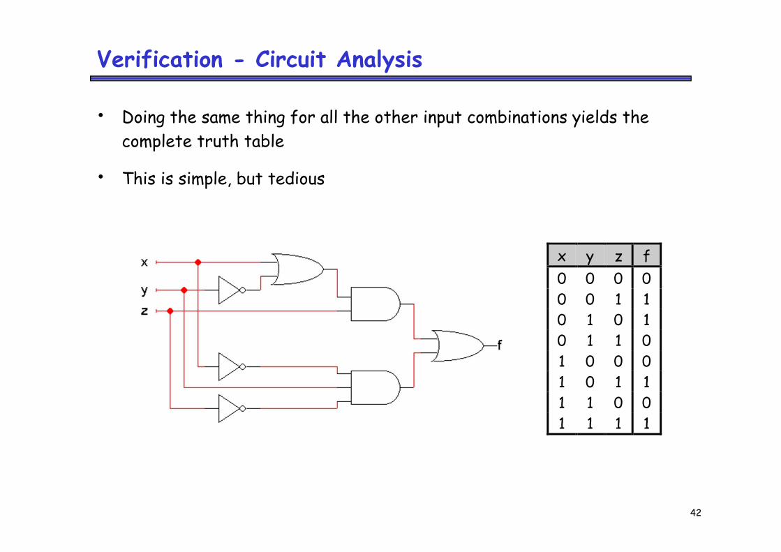
Verification - Circuit Analysis
• Doing the same thing for all the other input combinations yields thecomplete truth table
• This is simple, but tedious
x y z f0 0 0 00 0 1 10 1 0 10 1 1 01 0 0 01 0 1 11 1 0 01 1 1 1
43
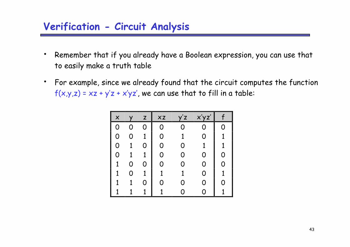
Verification - Circuit Analysis
• Remember that if you already have a Boolean expression, you can use thatto easily make a truth table
• For example, since we already found that the circuit computes the functionf(x,y,z) = xz + y’z + x’yz’, we can use that to fill in a table:
x y z xz y’z x’yz’ f0 0 0 0 0 0 00 0 1 0 1 0 10 1 0 0 0 1 10 1 1 0 0 0 01 0 0 0 0 0 01 0 1 1 1 0 11 1 0 0 0 0 01 1 1 1 0 0 1
44
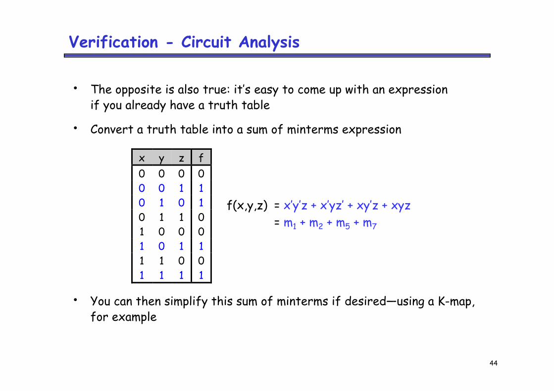
Verification - Circuit Analysis
• The opposite is also true: it’s easy to come up with an expression if you already have a truth table
• Convert a truth table into a sum of minterms expression
• You can then simplify this sum of minterms if desired—using a K-map, for example
x y z f0 0 0 00 0 1 10 1 0 10 1 1 01 0 0 01 0 1 11 1 0 01 1 1 1
f(x,y,z) = x’y’z + x’yz’ + xy’z + xyz= m1 + m2 + m5 + m7
45
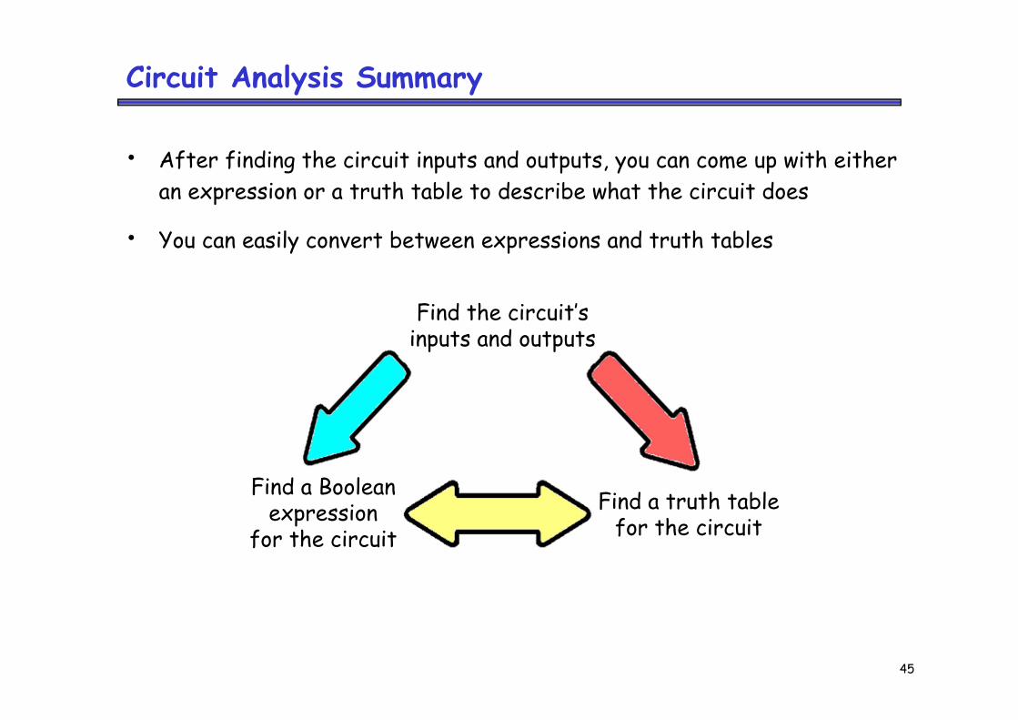
Circuit Analysis Summary
• After finding the circuit inputs and outputs, you can come up with either an expression or a truth table to describe what the circuit does
• You can easily convert between expressions and truth tables
Find the circuit’sinputs and outputs
Find a Booleanexpression
for the circuitFind a truth table
for the circuit