Chapter 2 Logic Functions and Gates. 2 Basic Logic Functions The three basic logic functions are:...
88
Chapter 2 Logic Functions and Gates
-
Upload
jeffry-banks -
Category
Documents
-
view
262 -
download
1
Transcript of Chapter 2 Logic Functions and Gates. 2 Basic Logic Functions The three basic logic functions are:...

Chapter 2
Logic Functions and Gates

2
Basic Logic Functions
• The three basic logic functions are:– AND– OR– NOT

3
Logic Function Representation
• Logic functions can be represented:–algebraically–using truth tables–using electronic circuits.

4
Algebraic Representation
• Uses Boolean algebra.
• Boolean variables have two states (binary).
• Boolean operators include AND, OR, and NOT.

5
Truth Table Representation
• Defines the output of a function for every possible combination of inputs.
• A system with n inputs has 2n possible combinations.

6
Electronic Circuit Representation
• Uses logic gates to perform Boolean algebraic functions.
• Gates can be represented by schematic symbols.
• Symbols can be either distinctive-shape or rectangular-outline.

7
Distinctive Shape Schematic Symbols
• Uses different graphic representations for different logic functions.
• Uses a bubble (a small circle) to indicate a logical inversion.

8
Rectangular-Outline Schematic Symbols
• All functions are shown in rectangular form with the logic function indicated by standard notation inside the rectangle.
• The notation specifying the logic function is called the qualifying symbol.
• Inversion is indicated by a 1/2 arrowhead.

9
NOT Function
• One input and one output.
• The output is the opposite logic level of the input.
• The output is the complement of the input.

10
NOT Function Boolean Representation
• Inversion is indicated by a bar over the signal to be inverted.
A Y

11
NOT Function Electronic Circuit
• Called a NOT gate or, more usually, an INVERTER.
• Distinctive-shape symbol is a triangle with inversion bubble.
• Rectangular-shape symbol uses “1” and the inversion 1/2 arrowhead.

12
NOT Function Electronic Circuit

13
AND Function
• Two or more inputs, one output.
• Output is HIGH only when all of the inputs are HIGH.
• Output is LOW whenever any input is LOW.

14
A B Y0 0 0
0 1 01 0 01 1 1
AND Function

15
AND Boolean Representation
• AND symbol is “•” or nothing at all.
ABY
B AY

16
AND Function Electronic Circuit
• Called an AND gate.
• Distinctive-shape symbol uses AND designation.
• Rectangular-shape symbol use “&” as designator.

17
AND Function Electronic Circuit

18
AND Function Electronic Circuit

19
A B C Y0 0 0 0
0 0 1 0
0 1 0 0
0 1 1 0
1 0 0 0
1 0 1 0
1 1 0 0
1 1 1 1
AND Function Electronic Circuit

20
OR Function
• Two or more inputs, one output.
• Output is HIGH whenever one or more input is HIGH.
• Output is LOW only when all of the inputs are LOW.

21
OR Function
A B Y
0 0 0
0 1 0
1 0 1
1 1 1

22
OR Boolean Representation
• OR symbol is “+”.
• Y = A + B

23
OR Function Electronic Circuit
• Called an OR gate.
• Distinctive-shape symbol uses OR designation.
• Rectangular-shape symbol uses “” as designator.

24
OR Function Electronic Circuit

25
Active Level
• The logic level defined as “ON” for a circuit.
• When a logic HIGH is “ON”, the signal is active-HIGH.
• When a logic LOW is “ON”, the signal is active-LOW.

26
NAND Function
• Generated by inverting the output of the AND function.
• Output is HIGH whenever any input is LOW.
• Output is LOW only when all inputs are HIGH.

27
NAND Function
A B Y
0 0 1
0 1 1
1 0 1
1 1 0

28
NAND Boolean Representation
• Uses AND with an inversion overbar.
BA Y

29
NAND Function Electronic Circuit
• Called a NAND gate.
• Uses the AND symbol with inversion on.

30
NAND Function Electronic Circuit

31
NOR Function
• Generated by inverting the output of the OR function.
• Output is HIGH only when all inputs are LOW.
• Outputs is LOW whenever any input is HIGH.

32
A B Y0 0 1
0 1 0
1 0 0
1 1 0
NOR Function

33
NOR Boolean Representation
• Uses OR with an inversion overbar.
B A Y

34
NOR Function Electronic Circuit
• Called a NOR gate.
• Uses OR symbol with inversion on the output.

35
NOR Function Electronic Circuit

36
3 Input NOR and NAND FunctionTruth Tables
• 3 Input NAND:
• 3 Input NOR:
CBA Y
C B A Y

37
A B C0 0 0 1 10 0 1 1 00 1 0 1 00 1 1 1 01 0 0 1 01 0 1 1 01 1 0 1 01 1 1 0 0
C B A CBA
3 Input NOR and NAND FunctionTruth Tables

38
Exclusive OR Gate
• Two inputs, one output.
• Output is HIGH when one, and only one, input is HIGH.
• Output is LOW when both inputs are equal – both HIGH or both LOW.

39
Exclusive OR Gate

40
A B Y0 0 0
0 1 1
1 0 1
1 1 0
Exclusive OR Gate

41
Exclusive NOR Gate
• Two inputs, one output.
• Output is HIGH when both inputs are equal – both HIGH or both LOW.
• Output is LOW when one, and only one, input is HIGH.

42
Exclusive NOR Gate

43
A B Y0 0 1
0 1 0
1 0 0
1 1 1
Exclusive NOR Gate

44
Gate Equivalence – NAND
• A NAND gate can be represented by an AND gate with inverted output.
• A NAND gate can be represented by an OR gate with inverted inputs.

45
Gate Equivalence – NAND

46
Gate Equivalence – NOR
• A NOR gate can be represented by an OR gate with inverted output.
• A NOR gate can be represented by an AND gate with inverted inputs.

47
Gate Equivalence – DeMorgan Forms
• Change an AND function to an OR function and an OR function to an AND function.
• Invert the inputs.
• Invert the outputs.

48
DeMorgan’s Theorem - 1
•
•
• Break the line and change the sign
B A BA B A BA

49
DeMorgan’s Theorem - 2
• The following are two common errors associated with DeMorgan’s Theorem:
•
• B A BA B A BA

50
Active Logic Levels
• Any INPUT or OUTPUT that has a BUBBLE is considered as active LOW.
• Any INPUT or OUTPUT that has no BUBBLE is considered as active HIGH.

51
Active Logic Levels - NOR
•
• At least one input HIGH makes the output LOW.
•
• All inputs LOW make the output HIGH.
BA Y
BA Y

52
Active Logic Levels - NOR

53
Logic Switches
• Provides a logic HIGH or LOW depending on switch position.
• Commonly used types include normally-open pushbutton, normally-closed pushbutton, single-pole single-throw, and single-pole double-throw.

54
Logic Switches

55
Logic Switches

56
Two-Pole Push Button
• Two-pole push button allows for normally HIGH and normally LOW levels from the same switch.

57
Two-Pole Push Button

58
Light Emitting Diodes (LED’s)
• Used to indicate the status of a digital output.
• Has two terminals the anode and the cathode.
• If the anode is approximately 1.5 V greater than the cathode, current flows and the LED illuminates.

59
Light Emitting Diodes (LED’s)

60
Light Emitting Diodes (LED’s)

61
Light Emitting Diodes
• Used to provide a visual indication of a logic state.
• Can be wired to display active-HIGH or active-LOW.

62
Light Emitting Diodes

63
Light Emitting Diodes

64
Logic Gate Enable
• The input to a gate that allows the output to respond to other inputs.
• A logic LOW for an OR or NOR gate, a logic HIGH for an AND or NAND gate.

65
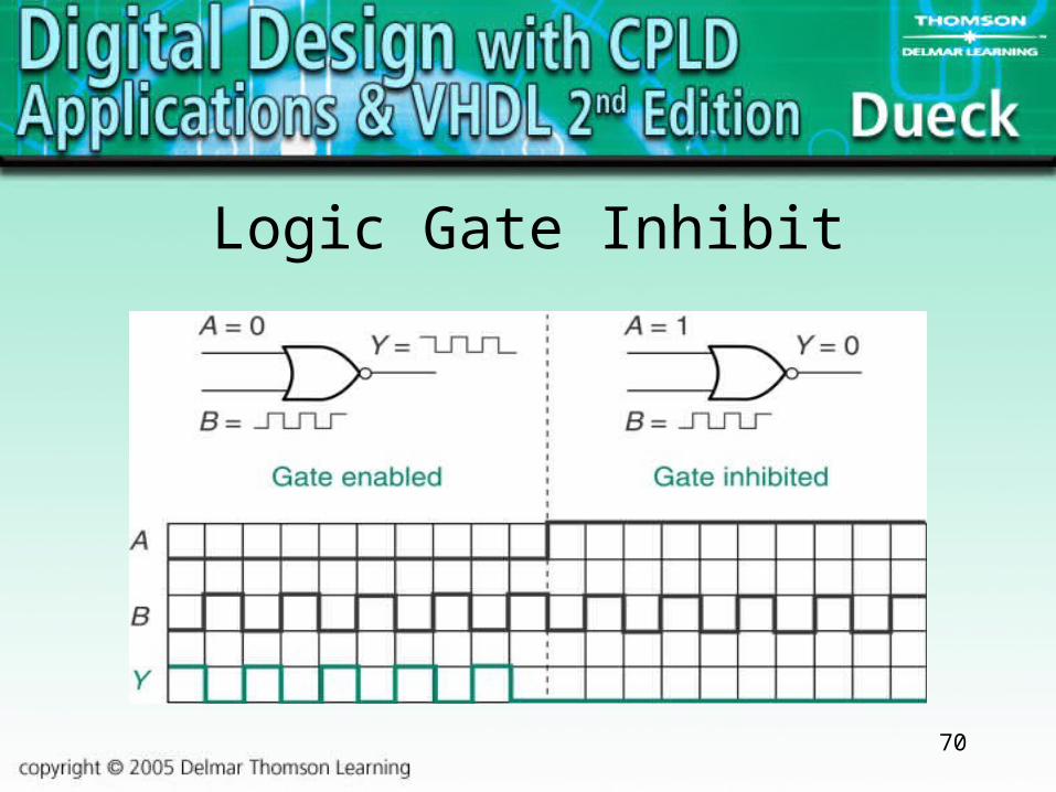
Logic Gate Inhibit
• The input to a gate that forces the output to ignore any other input.
• A logic HIGH for an OR or NOR gate, a logic LOW for an AND or NAND gate.

66
Logic Gate Inhibit

67
Logic Gate Inhibit

68
Logic Gate Inhibit

69
Logic Gate Inhibit
70
Logic Gate Inhibit

71
Logic Gate Inhibit

72
Control AND OR NAND NOR XOR XNOR
A = 0 Y = 0 Y = B Y = 1 Y = B
A = 1 Y = B Y = 1 Y = 0 Y = BB Y
B Y
B Y
B Y
Logic Gate Inhibit

73
Tristate Buffer
• Three output states, HIGH, LOW and high-impedance.
• Requires a separate input to control which output state is selected.

74
Tristate Buffer

75
Tristate Buffer

76
Tristate Buffer Utilization
• Used to connect multiple outputs together.
• Used in controlling the operation of buses.

77
Tristate Buffer Utilization

78
The 74LS244 Octal Tri-State Buffer
• Contains two groups of four non-inverting tri-state buffers.
• Each group is controlled by a separate enable input.
G

79
The 74LS244 Octal Tri-State Buffer

80
Integrated Circuit Package
• Integrated Circuits (ICs) contain many components in a single package.
• Several packaging options are available.
• One common package is called dual-in-line (DIP).

81
Integrated Circuit Package

82
Integrated Circuit Technology
• One common form is transistor-transistor logic, called TTL.
• The other common form is Complementary Metal-Oxide Semiconductor, called CMOS.

83
Part Number Logic Family74LS00 Low-power Schottky TTL
74ALS00 Advanced low-power Schottky TTL
74F00 FAST TTL
74HC00 High-speed CMOS
74CT00 High-speed CMOS (TTL-compatible inputs)
74LVX00 Low-voltage CMOS
74ABT00 Advanced BiCMOS (TTL/CMOS hybrid)
Integrated Circuit Technology

84
Integrated Circuit Designation
• Standard form is 74XXFF, where 74 is the logic family identifier, XX is the logic family member and FF identifies the specific logic function.
• SN74ALS00N

85
IC Package Options
• PLCC - plastic lead chip carrier • SOIC - small outline integrated circuit • TSSOP – thin shrink small outline
package• QFP – quad flat pack• DIP – dual inline package• BGA – ball grid array

86
IC Package Options

87
PLCC 84 Pin Packages• Can be mounted on the surface of a
circuit board or mounted in a socket.
• Pins are equally distributed on four sides.
• Pin 1 placed on the center of one of the rows, as indicated by a dot.
• Pins number counterclockwise from this point.

88
PLCC 84 Pin Packages