Chapter 11 Frequency Response - Islamic University of Gaza
74
CH 10 Differential Amplifiers 1 Chapter 11 Frequency Response 11.1 Fundamental Concepts 11.2 High-Frequency Models of Transistors 11.3 Analysis Procedure 11.4 Frequency Response of CE and CS Stages 11.5 Frequency Response of CB and CG Stages 11.6 Frequency Response of Followers 11.7 Frequency Response of Cascode Stage 11.8 Frequency Response of Differential Pairs 11.9 Additional Examples 1
Transcript of Chapter 11 Frequency Response - Islamic University of Gaza

CH 10 Differential Amplifiers 1
Chapter 11 Frequency Response
11.1 Fundamental Concepts
11.2 High-Frequency Models of Transistors
11.3 Analysis Procedure
11.4 Frequency Response of CE and CS Stages
11.5 Frequency Response of CB and CG Stages
11.6 Frequency Response of Followers
11.7 Frequency Response of Cascode Stage
11.8 Frequency Response of Differential Pairs
11.9 Additional Examples
1

CH 10 Differential Amplifiers 2
Chapter Outline
CH 11 Frequency Response 2

CH 10 Differential Amplifiers 3CH 11 Frequency Response 3
High Frequency Roll-off of Amplifier
As frequency of operation increases, the gain of amplifier
decreases. This chapter analyzes this problem.

CH 10 Differential Amplifiers 4
Example: Human Voice I
Natural human voice spans a frequency range from 20Hz to
20KHz, however conventional telephone system passes
frequencies from 400Hz to 3.5KHz. Therefore phone
conversation differs from face-to-face conversation. CH 11 Frequency Response 4
Natural Voice Telephone System

CH 10 Differential Amplifiers 5
Example: Human Voice II
CH 11 Frequency Response 5
Mouth RecorderAir
Mouth EarAir
Skull
Path traveled by the human voice to the voice recorder
Path traveled by the human voice to the human ear
Since the paths are different, the results will also be
different.
CH 10 Differential Amplifiers 6
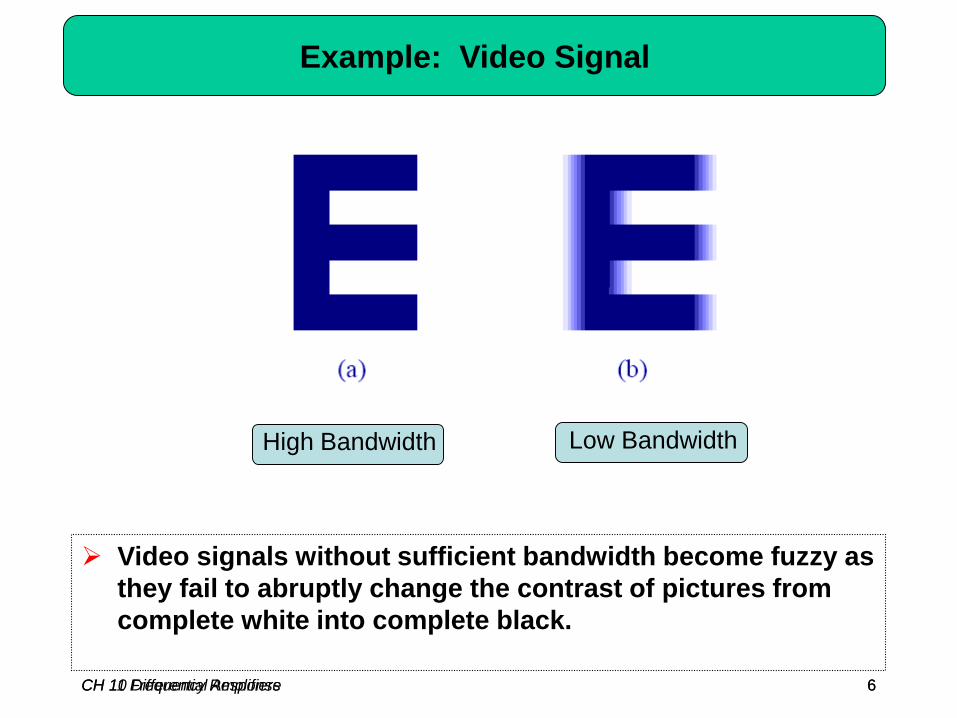
Example: Video Signal
Video signals without sufficient bandwidth become fuzzy as
they fail to abruptly change the contrast of pictures from
complete white into complete black.
CH 11 Frequency Response 6
High Bandwidth Low Bandwidth

CH 10 Differential Amplifiers 7
Gain Roll-off: Simple Low-pass Filter
In this simple example, as frequency increases the
impedance of C1 decreases and the voltage divider consists
of C1 and R1 attenuates Vin to a greater extent at the output. CH 11 Frequency Response 7

CH 10 Differential Amplifiers 8CH 11 Frequency Response 8
Gain Roll-off: Common Source
The capacitive load, CL, is the culprit for gain roll-off since at high frequency, it will “steal” away some signal current and shunt it to ground.
1||out m in D
L
V g V RC s

CH 10 Differential Amplifiers 9CH 11 Frequency Response 9
Frequency Response of the CS Stage
At low frequency, the capacitor is effectively open and the gain is flat. As frequency increases, the capacitor tends to a short and the gain starts to decrease. A special frequency is ω=1/(RDCL), where the gain drops by 3dB.
1222
LD
Dm
in
out
CR
Rg
V
V

CH 10 Differential Amplifiers 10CH 11 Frequency Response 10
Example: Figure of Merit
This metric quantifies a circuit’s gain, bandwidth, and
power dissipation. In the bipolar case, low temperature,
supply, and load capacitance mark a superior figure of
merit.
LCCT CVVMOF
1...

CH 10 Differential Amplifiers 11
Example: Relationship between Frequency
Response and Step Response
CH 11 Frequency Response 11
2 2 21 1
1
1H s j
R C
0
1 1
1 expout
tV t V u t
R C
The relationship is such that as R1C1 increases, the
bandwidth drops and the step response becomes slower.

CH 10 Differential Amplifiers 12CH 11 Frequency Response 12
Bode Plot
When we hit a zero, ωzj, the Bode magnitude rises with a
slope of +20dB/dec.
When we hit a pole, ωpj, the Bode magnitude falls with a
slope of -20dB/dec
21
21
0
11
11
)(
pp
zz
ss
ss
AsH
CH 10 Differential Amplifiers 13CH 11 Frequency Response 13
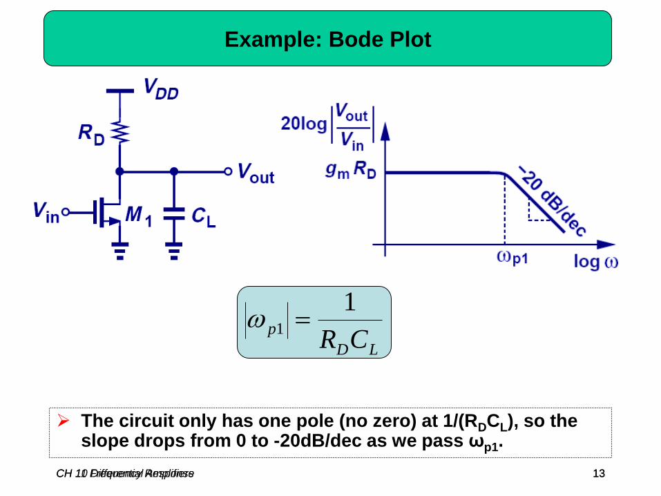
Example: Bode Plot
The circuit only has one pole (no zero) at 1/(RDCL), so the slope drops from 0 to -20dB/dec as we pass ωp1.
LD
pCR
11

CH 10 Differential Amplifiers 14CH 11 Frequency Response 14
Pole Identification Example I
inS
pCR
11
LD
pCR
12
2
2
22
1
2 11 pp
Dm
in
out Rg
V
V

CH 10 Differential Amplifiers 15CH 11 Frequency Response 15
Pole Identification Example II
in
m
S
p
Cg
R
1||
11
LD
pCR
12

CH 10 Differential Amplifiers 16CH 11 Frequency Response 16
Circuit with Floating Capacitor
The pole of a circuit is computed by finding the effective
resistance and capacitance from a node to GROUND.
The circuit above creates a problem since neither terminal
of CF is grounded.

CH 10 Differential Amplifiers 17CH 11 Frequency Response 17
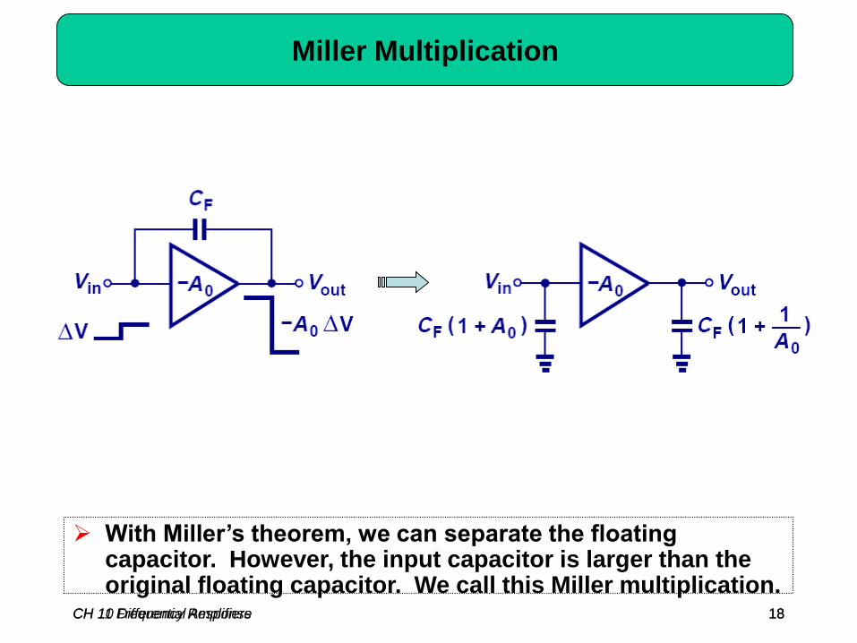
Miller’s Theorem
If Av is the gain from node 1 to 2, then a floating impedance
ZF can be converted to two grounded impedances Z1 and Z2.
v
F
A
ZZ
11
v
F
A
ZZ
/112
CH 10 Differential Amplifiers 18CH 11 Frequency Response 18
Miller Multiplication
With Miller’s theorem, we can separate the floating capacitor. However, the input capacitor is larger than the original floating capacitor. We call this Miller multiplication.

CH 10 Differential Amplifiers 19CH 11 Frequency Response 19
Example: Miller Theorem
FDmS
inCRgR
1
1
F
Dm
D
out
CRg
R
1
1
1

CH 10 Differential Amplifiers 20
High-Pass Filter Response
12
1
2
1
2
1
11
CR
CR
V
V
in
out
The voltage division between a resistor and a capacitor can be configured such that the gain at low frequency is reduced.
CH 11 Frequency Response 20

CH 10 Differential Amplifiers 21
Example: Audio Amplifier
nFCi 6.79 nFCL 8.39
In order to successfully pass audio band frequencies (20 Hz-20 KHz), large input and output capacitances are needed.
200/1
100
m
i
g
KR
CH 11 Frequency Response 21

CH 10 Differential Amplifiers 22
Capacitive Coupling vs. Direct Coupling
Capacitive coupling, also known as AC coupling, passes
AC signals from Y to X while blocking DC contents.
This technique allows independent bias conditions between
stages. Direct coupling does not.
Capacitive Coupling Direct Coupling
CH 11 Frequency Response 22

CH 10 Differential Amplifiers 23
Typical Frequency Response
Lower Corner Upper Corner
CH 11 Frequency Response 23

CH 10 Differential Amplifiers 24CH 11 Frequency Response 24
High-Frequency Bipolar Model
At high frequency, capacitive effects come into play. Cb
represents the base charge, whereas C and Cje are the
junction capacitances.
b jeC C C

CH 10 Differential Amplifiers 25CH 11 Frequency Response 25
High-Frequency Model of Integrated Bipolar
Transistor
Since an integrated bipolar circuit is fabricated on top of a
substrate, another junction capacitance exists between the
collector and substrate, namely CCS.

CH 10 Differential Amplifiers 26CH 11 Frequency Response 26
Example: Capacitance Identification

CH 10 Differential Amplifiers 27CH 11 Frequency Response 27
MOS Intrinsic Capacitances
For a MOS, there exist oxide capacitance from gate to channel, junction capacitances from source/drain to substrate, and overlap capacitance from gate to source/drain.

CH 10 Differential Amplifiers 28CH 11 Frequency Response 28
Gate Oxide Capacitance Partition and Full Model
The gate oxide capacitance is often partitioned between
source and drain. In saturation, C2 ~ Cgate, and C1 ~ 0. They
are in parallel with the overlap capacitance to form CGS and
CGD.

CH 10 Differential Amplifiers 29CH 11 Frequency Response 29
Example: Capacitance Identification

CH 10 Differential Amplifiers 30CH 11 Frequency Response 30
Transit Frequency
Transit frequency, fT, is defined as the frequency where the
current gain from input to output drops to 1.
C
gf mT 2
GS
mT
C
gf 2
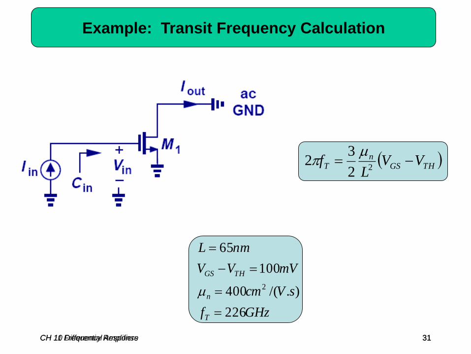
CH 10 Differential Amplifiers 31
Example: Transit Frequency Calculation
THGSn
T VVL
f 22
32
GHzf
sVcm
mVVV
nmL
T
n
THGS
226
)./(400
100
65
2
CH 11 Frequency Response 31

CH 10 Differential Amplifiers 32
Analysis Summary
The frequency response refers to the magnitude of the
transfer function.
Bode’s approximation simplifies the plotting of the
frequency response if poles and zeros are known.
In general, it is possible to associate a pole with each node
in the signal path.
Miller’s theorem helps to decompose floating capacitors
into grounded elements.
Bipolar and MOS devices exhibit various capacitances that
limit the speed of circuits.
CH 11 Frequency Response 32

CH 10 Differential Amplifiers 33
High Frequency Circuit Analysis Procedure
Determine which capacitor impact the low-frequency region
of the response and calculate the low-frequency pole
(neglect transistor capacitance).
Calculate the midband gain by replacing the capacitors with
short circuits (neglect transistor capacitance).
Include transistor capacitances.
Merge capacitors connected to AC grounds and omit those
that play no role in the circuit.
Determine the high-frequency poles and zeros.
Plot the frequency response using Bode’s rules or exact
analysis.
CH 11 Frequency Response 33
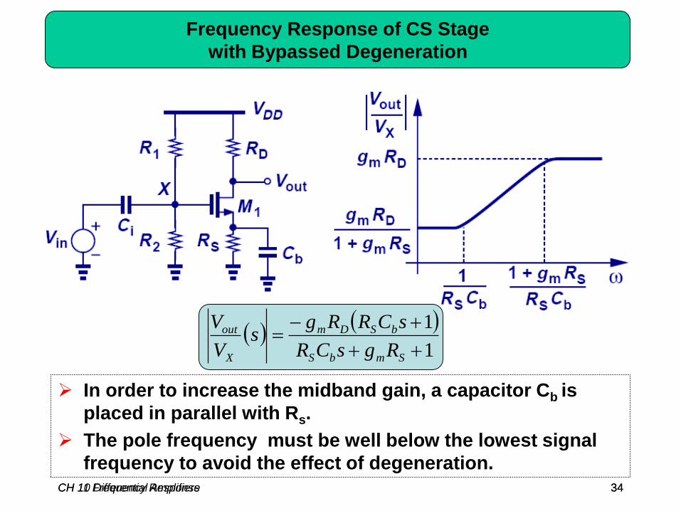
CH 10 Differential Amplifiers 34
Frequency Response of CS Stage
with Bypassed Degeneration
1
1
SmbS
bSDm
X
out
RgsCR
sCRRgs
V
V
In order to increase the midband gain, a capacitor Cb is
placed in parallel with Rs.
The pole frequency must be well below the lowest signal
frequency to avoid the effect of degeneration.CH 11 Frequency Response 34

CH 10 Differential Amplifiers 35CH 11 Frequency Response 35
Unified Model for CE and CS Stages

CH 10 Differential Amplifiers 36CH 11 Frequency Response 36
Unified Model Using Miller’s Theorem

CH 10 Differential Amplifiers 37
Example: CE Stage
fFC
fFC
fFC
mAI
R
CS
C
S
30
20
100
100
1
200
GHz
MHz
outp
inp
59.12
5162
,
,
The input pole is the bottleneck for speed.
CH 11 Frequency Response 37

CH 10 Differential Amplifiers 38
Example: Half Width CS Stage
XW 2
2
21
2
1
221
2
1
,
,
XY
Lm
outL
outp
XYLminS
inp
C
Rg
CR
CRgCR
CH 11 Frequency Response 38

CH 10 Differential Amplifiers 39CH 11 Frequency Response 39
Direct Analysis of CE and CS Stages
Direct analysis yields different pole locations and an extra zero.
outinXYoutXYinLThev
outXYLinThevThevXYLmp
outXYLinThevThevXYLm
p
XY
mz
CCCCCCRR
CCRCRRCRg
CCRCRRCRg
C
g
1||
1
1||
||
2
1
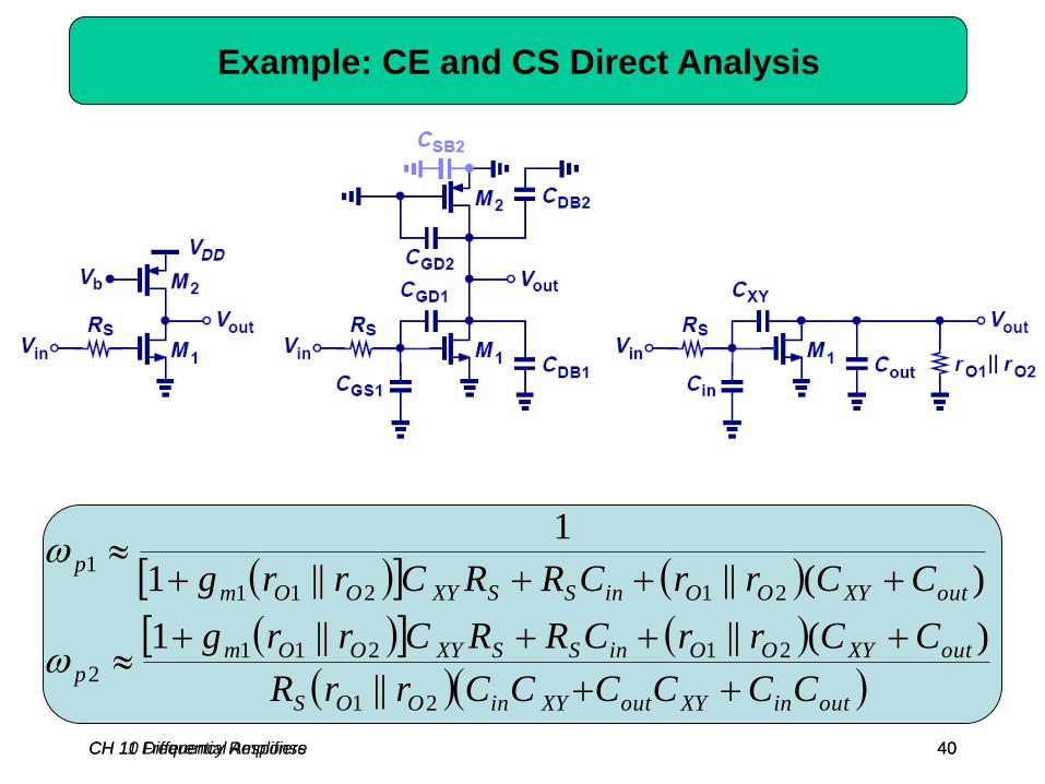
CH 10 Differential Amplifiers 40CH 11 Frequency Response 40
Example: CE and CS Direct Analysis
outinXYoutXYinOOS
outXYOOinSSXYOOmp
outXYOOinSSXYOOm
p
CCCCCCrrR
CCrrCRRCrrg
CCrrCRRCrrg
21
212112
21211
1
||
)(||||1
)(||||1
1
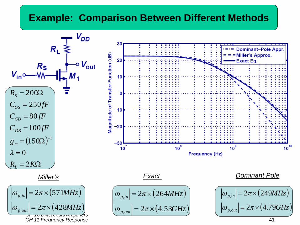
CH 10 Differential Amplifiers 41
Example: Comparison Between Different Methods
MHz
MHz
outp
inp
4282
5712
,
,
GHz
MHz
outp
inp
53.42
2642
,
,
GHz
MHz
outp
inp
79.42
2492
,
,
KR
g
fFC
fFC
fFC
R
L
m
DB
GD
GS
S
2
0
150
100
80
250
200
1
Miller’s Exact Dominant Pole
CH 11 Frequency Response 41

CH 10 Differential Amplifiers 42CH 11 Frequency Response 42
Input Impedance of CE and CS Stages
rsCRgC
ZCm
in ||1
1
sCRgCZ
GDDmGS
in
1
1

CH 10 Differential Amplifiers 43
Low Frequency Response of CB and CG Stages
miSm
iCm
in
out
gsCRg
sCRgs
V
V
1
As with CE and CS stages, the use of capacitive coupling
leads to low-frequency roll-off in CB and CG stages
(although a CB stage is shown above, a CG stage is
similar).
CH 11 Frequency Response 43

CH 10 Differential Amplifiers 44CH 11 Frequency Response 44
Frequency Response of CB Stage
X
m
S
Xp
Cg
R
1||
1,
CCX
YL
YpCR
1,
CSY CCC
Or

CH 10 Differential Amplifiers 45CH 11 Frequency Response 45
Frequency Response of CG Stage
Or
X
m
S
Xp
Cg
R
1||
1,
SBGSX CCC
YL
YpCR
1,
DBGDY CCC
Similar to a CB stage, the input pole is on the order of fT, so
rarely a speed bottleneck.
Or

CH 10 Differential Amplifiers 46CH 11 Frequency Response 46
Example: CG Stage Pole Identification
11
1
,1
||
1
GDSB
m
S
Xp
CCg
R
2211
2
, 1
1
DBGSGDDB
m
Yp
CCCCg

CH 10 Differential Amplifiers 47
Example: Frequency Response of CG Stage
KR
g
fFC
fFC
fFC
R
d
m
DB
GD
GS
S
2
0
150
100
80
250
200
1
MHz
GHz
Yp
Xp
4422
31.52
,
,
CH 11 Frequency Response 47

CH 10 Differential Amplifiers 48CH 11 Frequency Response 48
Emitter and Source Followers
The following will discuss the frequency response of
emitter and source followers using direct analysis.
Emitter follower is treated first and source follower is
derived easily by allowing r to go to infinity.
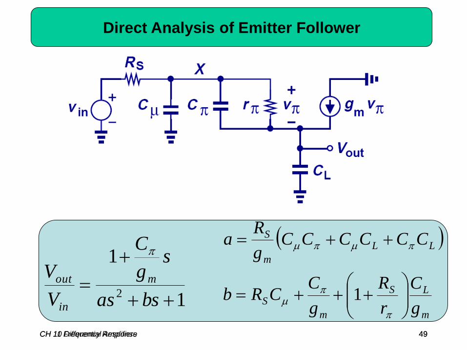
CH 10 Differential Amplifiers 49CH 11 Frequency Response 49
Direct Analysis of Emitter Follower
1
1
2
bsas
sg
C
V
V m
in
out
m
LS
m
S
LL
m
S
g
C
r
R
g
CCRb
CCCCCCg
Ra
1

CH 10 Differential Amplifiers 50CH 11 Frequency Response 50
Direct Analysis of Source Follower Stage
1
1
2
bsas
sg
C
V
V m
GS
in
out
m
SBGDGDS
SBGSSBGDGSGD
m
S
g
CCCRb
CCCCCCg
Ra
CH 10 Differential Amplifiers 51
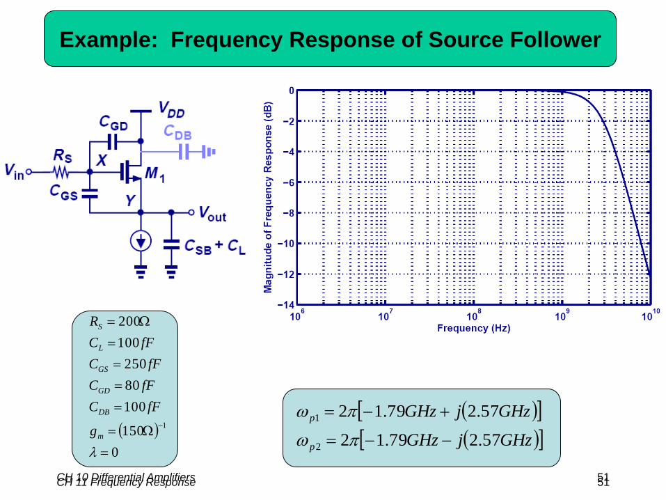
Example: Frequency Response of Source Follower
0
150
100
80
250
100
200
1
m
DB
GD
GS
L
S
g
fFC
fFC
fFC
fFC
R
GHzjGHz
GHzjGHz
p
p
57.279.12
57.279.12
2
1
CH 11 Frequency Response 51

CH 10 Differential Amplifiers 52CH 11 Frequency Response 52
Example: Source Follower
1
1
2
bsas
sg
C
V
V m
GS
in
out
1
22111
2211111
1
))((
m
DBGDSBGDGDS
DBGDSBGSGDGSGD
m
S
g
CCCCCRb
CCCCCCCg
Ra

CH 10 Differential Amplifiers 53CH 11 Frequency Response 53
Input Capacitance of Emitter/Source Follower
Lm
GSGDin
Rg
CCCCC
1
//
Or

CH 10 Differential Amplifiers 54CH 11 Frequency Response 54
Example: Source Follower Input Capacitance
1
211
1||1
1GS
OOm
GDin Crrg
CC

CH 10 Differential Amplifiers 55CH 11 Frequency Response 55
Output Impedance of Emitter Follower
1
sCr
RrsCrR
I
V SS
X
X

CH 10 Differential Amplifiers 56CH 11 Frequency Response 56
Output Impedance of Source Follower
mGS
GSS
X
X
gsC
sCR
I
V
1

CH 10 Differential Amplifiers 57CH 11 Frequency Response 57
Active Inductor
The plot above shows the output impedance of emitter and source followers. Since a follower’s primary duty is to lower the driving impedance (RS>1/gm), the “active inductor” characteristic on the right is usually observed.

CH 10 Differential Amplifiers 58CH 11 Frequency Response 58
Example: Output Impedance
33
321 1||
mGS
GSOO
X
X
gsC
sCrr
I
V
Or
CH 10 Differential Amplifiers 59CH 11 Frequency Response 59
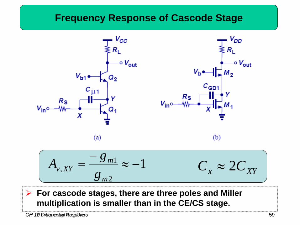
Frequency Response of Cascode Stage
For cascode stages, there are three poles and Miller
multiplication is smaller than in the CE/CS stage.
12
1,
m
mXYv
g
gA
XYx CC 2

CH 10 Differential Amplifiers 60CH 11 Frequency Response 60
Poles of Bipolar Cascode
111
,2||
1
CCrRS
Xp
121
2
,
21
1
CCCg
CS
m
Yp
22
,
1
CCR CSL
outp

CH 10 Differential Amplifiers 61CH 11 Frequency Response 61
Poles of MOS Cascode
1
2
11
,
1
1
GD
m
mGSS
Xp
Cg
gCR
1
1
221
2
,
11
1
GD
m
mGSDB
m
Yp
Cg
gCC
g
22
,
1
GDDBL
outpCCR

CH 10 Differential Amplifiers 62
Example: Frequency Response of Cascode
KR
g
fFC
fFC
fFC
R
L
m
DB
GD
GS
S
2
0
150
100
80
250
200
1
MHz
GHz
GHz
outp
Yp
Xp
4422
73.12
95.12
,
,
,
CH 11 Frequency Response 62

CH 10 Differential Amplifiers 63CH 11 Frequency Response 63
MOS Cascode Example
1
2
11
,
1
1
GD
m
mGSS
Xp
Cg
gCR
331
1
221
2
,
11
1
DBGDGD
m
mGSDB
m
Yp
CCCg
gCC
g
22
,
1
GDDBL
outpCCR

CH 10 Differential Amplifiers 64CH 11 Frequency Response 64
I/O Impedance of Bipolar Cascode
sCCrZ in
11
12
1||
sCC
RZCS
Lout
22
1||

CH 10 Differential Amplifiers 65CH 11 Frequency Response 65
I/O Impedance of MOS Cascode
sCg
gC
Z
GD
m
mGS
in
1
2
11 1
1
sCCRZ
DBGD
Lout
22
1||

CH 10 Differential Amplifiers 66CH 11 Frequency Response 66
Bipolar Differential Pair Frequency Response
Since bipolar differential pair can be analyzed using half-circuit, its transfer function, I/O impedances, locations of poles/zeros are the same as that of the half circuit’s.
Half Circuit

CH 10 Differential Amplifiers 67CH 11 Frequency Response 67
MOS Differential Pair Frequency Response
Since MOS differential pair can be analyzed using half-circuit, its transfer function, I/O impedances, locations of poles/zeros are the same as that of the half circuit’s.
Half Circuit

CH 10 Differential Amplifiers 68CH 11 Frequency Response 68
Example: MOS Differential Pair
33
,
1
1
331
3
,
1311
,
1
11
1
])/1([
1
GDDBL
outp
GD
m
mGSDB
m
Yp
GDmmGSS
Xp
CCR
Cg
gCC
g
CggCR

CH 10 Differential Amplifiers 69
Common Mode Frequency Response
12
1
SSmSSSS
SSSSDm
CM
out
RgsCR
CRRg
V
V
Css will lower the total impedance between point P to ground at high frequency, leading to higher CM gain which degrades the CM rejection ratio.
CH 11 Frequency Response 69

CH 10 Differential Amplifiers 70
Tail Node Capacitance Contribution
Source-Body Capacitance of M1, M2 and M3
Gate-Drain Capacitance of M3
CH 11 Frequency Response 70

CH 10 Differential Amplifiers 71
Example: Capacitive Coupling
EBin RrRR 1|| 222
Hz
CRr B
L 5422||
1
111
1
HzCRR inC
L 9.221
22
2
CH 11 Frequency Response 71

CH 10 Differential Amplifiers 72
MHz
CRR inD
L 92.621
221
2
MHzCR
Rg
S
SmL 4.422
1
11
111
2
21 v
Fin
A
RR
Example: IC Amplifier – Low Frequency Design
CH 11 Frequency Response 72

CH 10 Differential Amplifiers 73
77.3|| 211 inDm
in
X RRgv
v
Example: IC Amplifier – Midband Design
CH 11 Frequency Response 73
CH 10 Differential Amplifiers 74
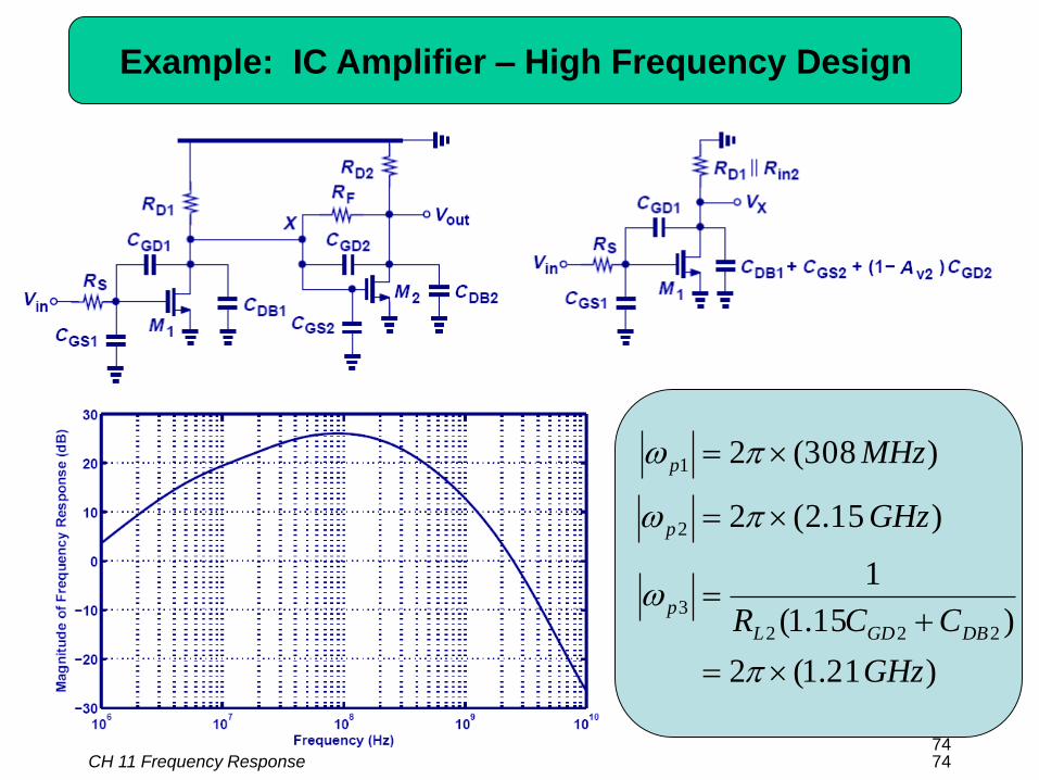
Example: IC Amplifier – High Frequency Design
)21.1(2
)15.1(
1
)15.2(2
)308(2
222
3
2
1
GHz
CCR
GHz
MHz
DBGDL
p
p
p
CH 11 Frequency Response 74