Chapter 1: Islamic University of Gaza Semiconductor Diodes...
21
Chapter 1: Semiconductor Diodes Islamic University of Gaza Dr. Talal Skaik
Transcript of Chapter 1: Islamic University of Gaza Semiconductor Diodes...

Chapter 1:
Semiconductor Diodes
Islamic University of Gaza
Dr. Talal Skaik

Copyright ©2009 by Pearson Education, Inc.
Upper Saddle River, New Jersey 07458 • All rights reserved.
Electronic Devices and Circuit Theory, 10/e Robert L. Boylestad and Louis Nashelsky
The Zener region is in the diode’s reverse-bias region.
At some point the reverse bias voltage is so large the
diode breaks down and the reverse current increases
dramatically.
Zener Region
• The maximum reverse voltage
that won’t take a diode into the
zener region is called the peak
inverse voltage (PIV) or peak
reverse voltage (PRV).
• The voltage that causes a diode
to enter the zener region of
operation is called the zener
voltage (VZ).
2 Dr. Talal Skaik 2014

Copyright ©2009 by Pearson Education, Inc.
Upper Saddle River, New Jersey 07458 • All rights reserved.
Electronic Devices and Circuit Theory, 10/e Robert L. Boylestad and Louis Nashelsky
The point at which the diode changes from no-bias condition to
forward-bias condition occurs when the electrons and holes are
given sufficient energy to cross the p-n junction. This energy
comes from the external voltage applied across the diode.
Forward Bias Voltage
The forward bias voltage required for a:
• gallium arsenide diode 1.2 V
• silicon diode 0.7 V
• germanium diode 0.3 V
3 Dr. Talal Skaik 2014

Copyright ©2009 by Pearson Education, Inc.
Upper Saddle River, New Jersey 07458 • All rights reserved.
Electronic Devices and Circuit Theory, 10/e Robert L. Boylestad and Louis Nashelsky
Comparison Ge, Si, GaAs
4 Dr. Talal Skaik 2014

Copyright ©2009 by Pearson Education, Inc.
Upper Saddle River, New Jersey 07458 • All rights reserved.
Electronic Devices and Circuit Theory, 10/e Robert L. Boylestad and Louis Nashelsky
As temperature increases it adds energy to the diode.
• It reduces the required forward bias voltage for forward-bias
conduction.
• It increases the amount of reverse current in the reverse-bias
condition.
Germanium diodes are more sensitive to temperature variations
than silicon or gallium arsenide diodes.
Temperature Effects
5 Dr. Talal Skaik 2014

Copyright ©2009 by Pearson Education, Inc.
Upper Saddle River, New Jersey 07458 • All rights reserved.
Electronic Devices and Circuit Theory, 10/e Robert L. Boylestad and Louis Nashelsky
Temperature Effects
6 Dr. Talal Skaik 2014

Copyright ©2009 by Pearson Education, Inc.
Upper Saddle River, New Jersey 07458 • All rights reserved.
Electronic Devices and Circuit Theory, 10/e Robert L. Boylestad and Louis Nashelsky
Semiconductors react differently to DC and AC currents.
There are three types of resistance:
• DC (static) resistance
• AC (dynamic) resistance
• Average AC resistance
Resistance Levels
7 Dr. Talal Skaik 2014

Copyright ©2009 by Pearson Education, Inc.
Upper Saddle River, New Jersey 07458 • All rights reserved.
Electronic Devices and Circuit Theory, 10/e Robert L. Boylestad and Louis Nashelsky
DC (Static) Resistance
For a specific applied DC voltage
VD, the diode has a specific current
ID, and a specific resistance RD.
D
DD
I
VR
8 Dr. Talal Skaik 2014

Copyright ©2009 by Pearson Education, Inc.
Upper Saddle River, New Jersey 07458 • All rights reserved.
Electronic Devices and Circuit Theory, 10/e Robert L. Boylestad and Louis Nashelsky
AC (Dynamic) Resistance
9
The dynamic resistance is the resistance
offered by the diode to the AC signal. Is is
equal to the slope of the VI characteristics
(dV/dI or ΔV/ ΔI ) ,
change in voltage
resulting change in currentD
dV Vr
dI I
Dr. Talal Skaik 2014

Copyright ©2009 by Pearson Education, Inc.
Upper Saddle River, New Jersey 07458 • All rights reserved.
Electronic Devices and Circuit Theory, 10/e Robert L. Boylestad and Louis Nashelsky
AC (Dynamic) Resistance
10
/ /
o
23
19
sin -1 ,
1 , sin ,
n=1, and at room temperature of 27 C, T=273+27=300K
1.38 1026
1.6 10
D T D TV nV V nVsDD s
D T
D D DD s D s
D T D T
D TD
D D
T
IdIce I I e e
dV nV
dI dI II I ce I I
dV nV dV nV
dV nVr
dI I
for
KTV mV
q
26D
D
mVr
I
Dr. Talal Skaik 2014

Copyright ©2009 by Pearson Education, Inc.
Upper Saddle River, New Jersey 07458 • All rights reserved.
Electronic Devices and Circuit Theory, 10/e Robert L. Boylestad and Louis Nashelsky
• The resistance depends on the amount of current (ID) in the diode.
• rD = 26 mV/ID is the resistance of the p-n junction and does not
include the resistance of the semiconductor material itself (the body
resistance).
• rB is added to account for body resistance and it ranges from a
typical 0.1 to 2 .
AC (Dynamic) Resistance
B
D
d rI
r mV 26
rd
In the forward bias region:
In the reverse bias region:
The resistance is effectively infinite. The diode acts like an open.
11 Dr. Talal Skaik 2014
Copyright ©2009 by Pearson Education, Inc.
Upper Saddle River, New Jersey 07458 • All rights reserved.
Electronic Devices and Circuit Theory, 10/e Robert L. Boylestad and Louis Nashelsky
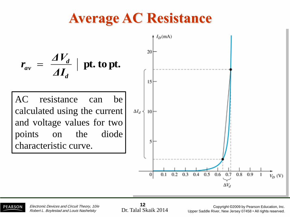
AC resistance can be
calculated using the current
and voltage values for two
points on the diode
characteristic curve.
Average AC Resistance
pt. to pt. d
dav
ΔI
ΔV r
12 Dr. Talal Skaik 2014

Copyright ©2009 by Pearson Education, Inc.
Upper Saddle River, New Jersey 07458 • All rights reserved.
Electronic Devices and Circuit Theory, 10/e Robert L. Boylestad and Louis Nashelsky
Diode Equivalent Circuit
13 Dr. Talal Skaik 2014
Copyright ©2009 by Pearson Education, Inc.
Upper Saddle River, New Jersey 07458 • All rights reserved.
Electronic Devices and Circuit Theory, 10/e Robert L. Boylestad and Louis Nashelsky
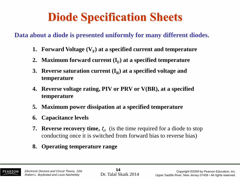
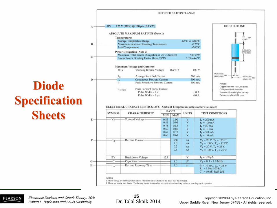
1. Forward Voltage (VF) at a specified current and temperature
2. Maximum forward current (IF) at a specified temperature
3. Reverse saturation current (IR) at a specified voltage and
temperature
4. Reverse voltage rating, PIV or PRV or V(BR), at a specified
temperature
5. Maximum power dissipation at a specified temperature
6. Capacitance levels
7. Reverse recovery time, trr (is the time required for a diode to stop
conducting once it is switched from forward bias to reverse bias)
8. Operating temperature range
Diode Specification Sheets
Data about a diode is presented uniformly for many different diodes.
14 Dr. Talal Skaik 2014
Copyright ©2009 by Pearson Education, Inc.
Upper Saddle River, New Jersey 07458 • All rights reserved.
Electronic Devices and Circuit Theory, 10/e Robert L. Boylestad and Louis Nashelsky
Diode
Specification
Sheets
15 Dr. Talal Skaik 2014

Copyright ©2009 by Pearson Education, Inc.
Upper Saddle River, New Jersey 07458 • All rights reserved.
Electronic Devices and Circuit Theory, 10/e Robert L. Boylestad and Louis Nashelsky
The anode is abbreviated A
The cathode is abbreviated K
Diode Symbol and Packaging
16 Dr. Talal Skaik 2014

Copyright ©2009 by Pearson Education, Inc.
Upper Saddle River, New Jersey 07458 • All rights reserved.
Electronic Devices and Circuit Theory, 10/e Robert L. Boylestad and Louis Nashelsky
An ohmmeter set on a low Ohms scale can be used
to test a diode. The diode should be tested out of
circuit.
Diode Testing - Ohmmeter
17 Dr. Talal Skaik 2014

Copyright ©2009 by Pearson Education, Inc.
Upper Saddle River, New Jersey 07458 • All rights reserved.
Electronic Devices and Circuit Theory, 10/e Robert L. Boylestad and Louis Nashelsky
Other Types of Diodes
Zener diode
Light-emitting diode
Diode arrays
18 Dr. Talal Skaik 2014
Copyright ©2009 by Pearson Education, Inc.
Upper Saddle River, New Jersey 07458 • All rights reserved.
Electronic Devices and Circuit Theory, 10/e Robert L. Boylestad and Louis Nashelsky
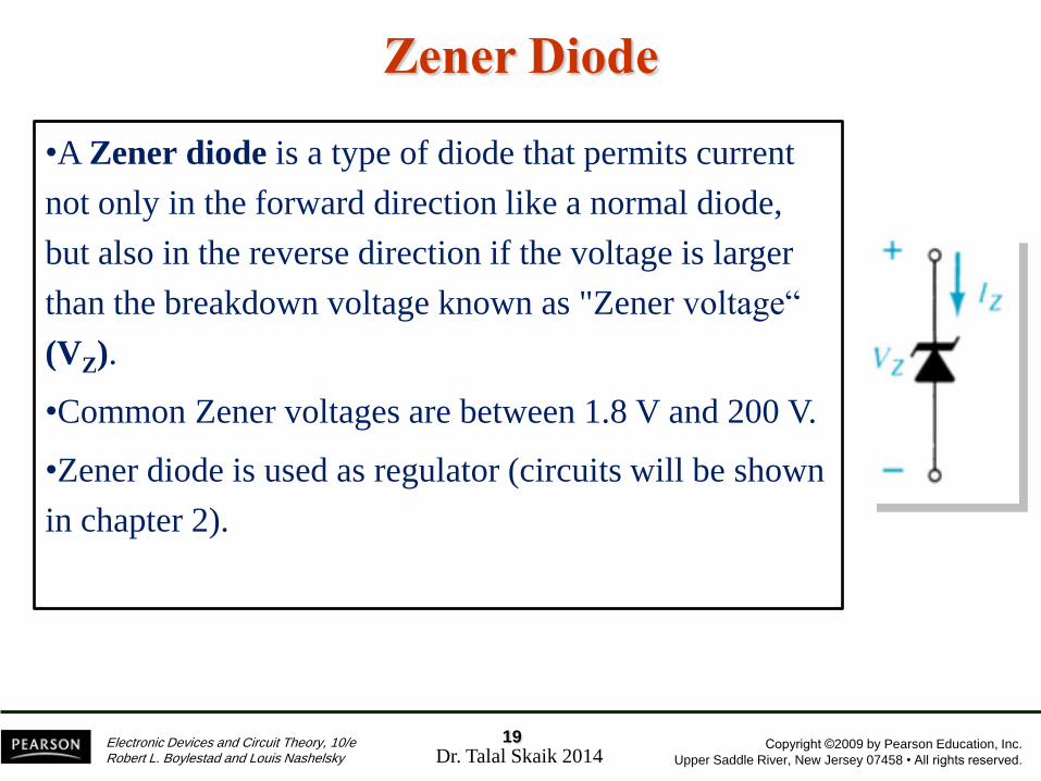
Zener Diode
19
•A Zener diode is a type of diode that permits current
not only in the forward direction like a normal diode,
but also in the reverse direction if the voltage is larger
than the breakdown voltage known as "Zener voltage“
(VZ).
•Common Zener voltages are between 1.8 V and 200 V.
•Zener diode is used as regulator (circuits will be shown
in chapter 2).
Dr. Talal Skaik 2014

Copyright ©2009 by Pearson Education, Inc.
Upper Saddle River, New Jersey 07458 • All rights reserved.
Electronic Devices and Circuit Theory, 10/e Robert L. Boylestad and Louis Nashelsky
Light-Emitting Diode (LED)
•An LED emits photons when it is forward biased.
•These can be in the infrared or visible spectrum.
•The forward bias voltage is usually in the range of 2 V to 5 V.
20
Color Construction Typical Forward
Voltage (V)
Amber AlInGaP 2.1
Blue GaN 5.0
Green GaP 2.2
Orange GaAsP 2.0
Red GaAsP 1.8
White GaN 4.1
Yellow AlInGaP 2.1
Light-Emitting Diodes
Dr. Talal Skaik 2014

Copyright ©2009 by Pearson Education, Inc.
Upper Saddle River, New Jersey 07458 • All rights reserved.
Electronic Devices and Circuit Theory, 10/e Robert L. Boylestad and Louis Nashelsky
Multiple diodes can be
packaged together in an
integrated circuit (IC).
Common Anode
Common Cathode
A variety of combinations
exist.
Diode Arrays
21 Dr. Talal Skaik 2014


![Semiconductor Diodes [Demo]](https://static.fdocuments.us/doc/165x107/577d294d1a28ab4e1ea66956/semiconductor-diodes-demo.jpg)