CC2662R-Q1 SimpleLink Wireless BMS MCU datasheet
47
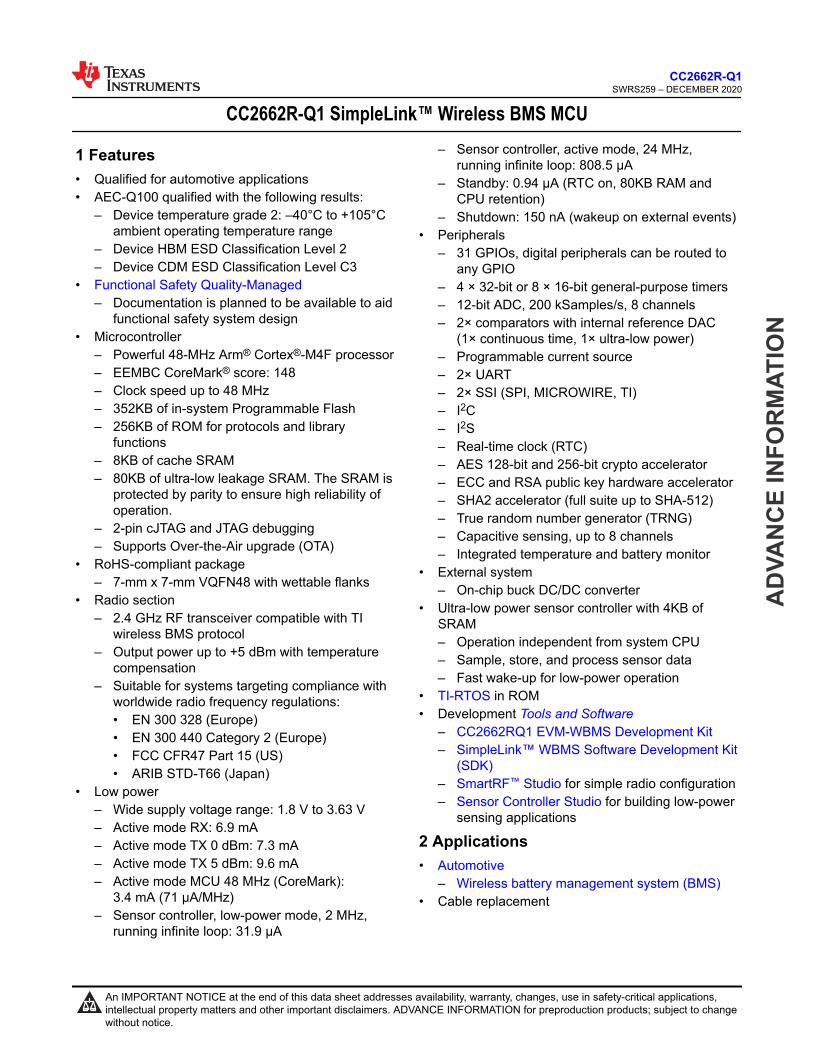
CC2662R-Q1 SimpleLink™ Wireless BMS MCU 1 Features • Qualified for automotive applications • AEC-Q100 qualified with the following results: – Device temperature grade 2: –40°C to +105°C ambient operating temperature range – Device HBM ESD Classification Level 2 – Device CDM ESD Classification Level C3 • Functional Safety Quality-Managed – Documentation is planned to be available to aid functional safety system design • Microcontroller – Powerful 48-MHz Arm ® Cortex ® -M4F processor – EEMBC CoreMark ® score: 148 – Clock speed up to 48 MHz – 352KB of in-system Programmable Flash – 256KB of ROM for protocols and library functions – 8KB of cache SRAM – 80KB of ultra-low leakage SRAM. The SRAM is protected by parity to ensure high reliability of operation. – 2-pin cJTAG and JTAG debugging – Supports Over-the-Air upgrade (OTA) • RoHS-compliant package – 7-mm x 7-mm VQFN48 with wettable flanks • Radio section – 2.4 GHz RF transceiver compatible with TI wireless BMS protocol – Output power up to +5 dBm with temperature compensation – Suitable for systems targeting compliance with worldwide radio frequency regulations: • EN 300 328 (Europe) • EN 300 440 Category 2 (Europe) • FCC CFR47 Part 15 (US) • ARIB STD-T66 (Japan) • Low power – Wide supply voltage range: 1.8 V to 3.63 V – Active mode RX: 6.9 mA – Active mode TX 0 dBm: 7.3 mA – Active mode TX 5 dBm: 9.6 mA – Active mode MCU 48 MHz (CoreMark): 3.4 mA (71 μA/MHz) – Sensor controller, low-power mode, 2 MHz, running infinite loop: 31.9 μA – Sensor controller, active mode, 24 MHz, running infinite loop: 808.5 μA – Standby: 0.94 µA (RTC on, 80KB RAM and CPU retention) – Shutdown: 150 nA (wakeup on external events) • Peripherals – 31 GPIOs, digital peripherals can be routed to any GPIO – 4 × 32-bit or 8 × 16-bit general-purpose timers – 12-bit ADC, 200 kSamples/s, 8 channels – 2× comparators with internal reference DAC (1× continuous time, 1× ultra-low power) – Programmable current source – 2× UART – 2× SSI (SPI, MICROWIRE, TI) – I 2 C – I 2 S – Real-time clock (RTC) – AES 128-bit and 256-bit crypto accelerator – ECC and RSA public key hardware accelerator – SHA2 accelerator (full suite up to SHA-512) – True random number generator (TRNG) – Capacitive sensing, up to 8 channels – Integrated temperature and battery monitor • External system – On-chip buck DC/DC converter • Ultra-low power sensor controller with 4KB of SRAM – Operation independent from system CPU – Sample, store, and process sensor data – Fast wake-up for low-power operation • TI-RTOS in ROM • Development Tools and Software – CC2662RQ1 EVM-WBMS Development Kit – SimpleLink™ WBMS Software Development Kit (SDK) – SmartRF ™ Studio for simple radio configuration – Sensor Controller Studio for building low-power sensing applications 2 Applications • Automotive – Wireless battery management system (BMS) • Cable replacement www.ti.com CC2662R-Q1 SWRS259 – DECEMBER 2020 ADVANCE INFORMATION Copyright © 2020 Texas Instruments Incorporated Submit Document Feedback 1 Product Folder Links: CC2662R-Q1 CC2662R-Q1 SWRS259 – DECEMBER 2020 An IMPORTANT NOTICE at the end of this data sheet addresses availability, warranty, changes, use in safety-critical applications, intellectual property matters and other important disclaimers. ADVANCE INFORMATION for preproduction products; subject to change without notice.
Transcript of CC2662R-Q1 SimpleLink Wireless BMS MCU datasheet
CC2662R-Q1 SimpleLink™ Wireless BMS MCU
1 Features• Qualified for automotive applications• AEC-Q100 qualified with the following results:
– Device temperature grade 2: –40°C to +105°Cambient operating temperature range
– Device HBM ESD Classification Level 2– Device CDM ESD Classification Level C3
• Functional Safety Quality-Managed– Documentation is planned to be available to aid
functional safety system design• Microcontroller
– Powerful 48-MHz Arm® Cortex®-M4F processor– EEMBC CoreMark® score: 148– Clock speed up to 48 MHz– 352KB of in-system Programmable Flash– 256KB of ROM for protocols and library
functions– 8KB of cache SRAM– 80KB of ultra-low leakage SRAM. The SRAM is
protected by parity to ensure high reliability ofoperation.
– 2-pin cJTAG and JTAG debugging– Supports Over-the-Air upgrade (OTA)
• RoHS-compliant package– 7-mm x 7-mm VQFN48 with wettable flanks
• Radio section– 2.4 GHz RF transceiver compatible with TI
wireless BMS protocol– Output power up to +5 dBm with temperature
compensation– Suitable for systems targeting compliance with
worldwide radio frequency regulations:• EN 300 328 (Europe)• EN 300 440 Category 2 (Europe)• FCC CFR47 Part 15 (US)• ARIB STD-T66 (Japan)
• Low power– Wide supply voltage range: 1.8 V to 3.63 V– Active mode RX: 6.9 mA– Active mode TX 0 dBm: 7.3 mA– Active mode TX 5 dBm: 9.6 mA– Active mode MCU 48 MHz (CoreMark):
3.4 mA (71 μA/MHz)– Sensor controller, low-power mode, 2 MHz,
running infinite loop: 31.9 μA
– Sensor controller, active mode, 24 MHz,running infinite loop: 808.5 μA
– Standby: 0.94 µA (RTC on, 80KB RAM andCPU retention)
– Shutdown: 150 nA (wakeup on external events)• Peripherals
– 31 GPIOs, digital peripherals can be routed toany GPIO
– 4 × 32-bit or 8 × 16-bit general-purpose timers– 12-bit ADC, 200 kSamples/s, 8 channels– 2× comparators with internal reference DAC
(1× continuous time, 1× ultra-low power)– Programmable current source– 2× UART– 2× SSI (SPI, MICROWIRE, TI)– I2C– I2S– Real-time clock (RTC)– AES 128-bit and 256-bit crypto accelerator– ECC and RSA public key hardware accelerator– SHA2 accelerator (full suite up to SHA-512)– True random number generator (TRNG)– Capacitive sensing, up to 8 channels– Integrated temperature and battery monitor
• External system– On-chip buck DC/DC converter
• Ultra-low power sensor controller with 4KB ofSRAM– Operation independent from system CPU– Sample, store, and process sensor data– Fast wake-up for low-power operation
• TI-RTOS in ROM• Development Tools and Software
– CC2662RQ1 EVM-WBMS Development Kit– SimpleLink™ WBMS Software Development Kit
(SDK)– SmartRF™ Studio for simple radio configuration– Sensor Controller Studio for building low-power
sensing applications
2 Applications• Automotive
– Wireless battery management system (BMS)• Cable replacement
www.ti.comCC2662R-Q1
SWRS259 – DECEMBER 2020
AD
VAN
CE
INFO
RM
ATIO
N
Copyright © 2020 Texas Instruments Incorporated Submit Document Feedback 1
Product Folder Links: CC2662R-Q1
CC2662R-Q1SWRS259 – DECEMBER 2020
An IMPORTANT NOTICE at the end of this data sheet addresses availability, warranty, changes, use in safety-critical applications,intellectual property matters and other important disclaimers. ADVANCE INFORMATION for preproduction products; subject to changewithout notice.

3 DescriptionThe SimpleLink™ 2.4 GHz CC2662R-Q1 device is an AEC-Q100 compliant wireless microcontroller(MCU) targeting wireless automotive applications. The device is optimized for low-power wirelesscommunication in applications such as battery management systems (BMS) and cable replacement. Thehighlighted features of this device include:• Support for TI wireless BMS protocol for robust, low latency and high throughput communication.• Functional Safety Quality-Managed classification including TI quality-managed development process and
forthcoming functional safety FIT rate calculation, FMEDA and functional safety documentation.• AEC-Q100 qualified at the Grade 2 temperature range (–40 °C to +105 °C) and is offered in a
7-mm x 7-mm VQFN package with wettable flanks.• Low standby current of 0.94 μA with full RAM retention.• Excellent radio link budget of 97 dBm.
The CC2662R-Q1 device is part of the SimpleLink™ MCU platform, which consists of Wi-Fi®, Bluetooth LowEnergy, Thread, Zigbee®, Sub-1 GHz MCUs, and host MCUs that all share a common, easy-to-use developmentenvironment and rich tool set. For more information, visit SimpleLink™ MCU platform.
Device Information (1)
PART NUMBER(2) PACKAGE BODY SIZE (NOM)XCC2662R1FTWRGZRQ1 VQFN (48) 7.00 mm × 7.00 mm
(1) For the most current part, package, and ordering information for all available devices, see the Package Option Addendum in Section12, or see the TI website.
(2) IMPORTANT NOTICE: The provided package DOES NOT represent the final, wettable flank package. The footprint is identical. Earlysamples should NOT be used for product qualification.
CC2662R-Q1SWRS259 – DECEMBER 2020 www.ti.com
AD
VAN
CE IN
FOR
MATIO
N
2 Submit Document Feedback Copyright © 2020 Texas Instruments Incorporated
Product Folder Links: CC2662R-Q1

4 Functional Block Diagram
Main CPU
Up to 352KBFlash
with 8KB Cache
Sensor Interface
cJTAG
Up to80KBSRAM
with Parity
256KBROM
Arm®
Cortex®-M4F Processor
LDO, Clocks, and ReferencesOptional DC/DC Converter
RF Core
Arm®
Cortex®-M0 Processor
DSP Modem
16KB SRAM
ROM
Sensor Controller
2x Low-Power Comparator
12-bit ADC, 200 ks/s
Capacitive Touch IF
SPI-I2C Digital Sensor IF
4KB SRAM
Time-to-Digital Converter
General Hardware Peripherals and Modules
4× 32-bit Timers
2× SSI (SPI)
Watchdog Timer
Temperature and Battery Monitor
RTC
I2C and I2S
2× UART
32 ch. µDMA
31 GPIOs
AES-256, SHA2-512
ECC, RSA
ADC
ADC
Digital PLL
48 MHz71 µA/MHz (3.0 V)
2.4 GHz
TRNG
8-bit DAC
Figure 4-1. CC2662R-Q1 Block Diagram
www.ti.comCC2662R-Q1
SWRS259 – DECEMBER 2020
AD
VAN
CE
INFO
RM
ATIO
N
Copyright © 2020 Texas Instruments Incorporated Submit Document Feedback 3
Product Folder Links: CC2662R-Q1

Table of Contents1 Features............................................................................12 Applications..................................................................... 13 Description.......................................................................24 Functional Block Diagram.............................................. 35 Revision History.............................................................. 46 Device Comparison......................................................... 57 Terminal Configuration and Functions..........................6
7.1 Pin Diagram – RGZ Package (Top View)....................67.2 Signal Descriptions..................................................... 77.3 Connections for Unused Pins and Modules................8
8 Specifications.................................................................. 98.1 Absolute Maximum Ratings ....................................... 98.2 ESD Ratings .............................................................. 98.3 Recommended Operating Conditions ........................98.4 Power Supply and Modules ....................................... 98.5 Power Consumption - Power Modes ....................... 108.6 Power Consumption - Radio Modes ........................ 118.7 Nonvolatile (Flash) Memory Characteristics ............ 118.8 Thermal Resistance Characteristics ........................ 118.9 Proprietary WBMS - Receive (RX) ...........................128.10 Proprietary WBMS - Transmit (TX) ........................ 138.11 Timing and Switching Characteristics..................... 138.12 Peripheral Characteristics.......................................18
9 Detailed Description......................................................259.1 Overview................................................................... 259.2 System CPU............................................................. 25
9.3 Radio (RF Core)........................................................269.4 Memory..................................................................... 279.5 Sensor Controller...................................................... 289.6 Cryptography............................................................ 299.7 Timers....................................................................... 309.8 Serial Peripherals and I/O.........................................319.9 Battery and Temperature Monitor............................. 319.10 µDMA......................................................................319.11 Debug......................................................................319.12 Power Management................................................329.13 Clock Systems........................................................ 339.14 Network Processor..................................................33
10 Application, Implementation, and Layout................. 3410.1 Reference Designs................................................. 3410.2 Junction Temperature Calculation...........................35
11 Device and Documentation Support..........................3611.1 Tools and Software..................................................3611.2 Documentation Support.......................................... 3811.3 Support Resources................................................. 3911.4 Trademarks............................................................. 3911.5 Electrostatic Discharge Caution.............................. 3911.6 Glossary.................................................................. 39
12 Mechanical, Packaging, and OrderableInformation.................................................................... 4012.1 Packaging Information............................................ 40
5 Revision HistoryDATE REVISION NOTESDecember 2020 * Initial Release
CC2662R-Q1SWRS259 – DECEMBER 2020 www.ti.com
AD
VAN
CE IN
FOR
MATIO
N
4 Submit Document Feedback Copyright © 2020 Texas Instruments Incorporated
Product Folder Links: CC2662R-Q1

6 Device ComparisonTable 6-1. Device Family Overview
DEVICE RADIO SUPPORT FLASH(KB)
RAM(KB) GPIO PACKAGE SIZE
CC1312R Sub-1 GHz 352 80 30 RGZ (7-mm × 7-mm VQFN48)
CC1352P
MultiprotocolSub-1 GHz
Bluetooth 5.1 Low EnergyZigbeeThread
2.4 GHz proprietary FSK-based formats+20-dBm high-power amplifier
352 80 26 RGZ (7-mm × 7-mm VQFN48)
CC1352R
MultiprotocolSub-1 GHz
Bluetooth 5.1 Low EnergyZigbeeThread
2.4 GHz proprietary FSK-based formats
352 80 28 RGZ (7-mm × 7-mm VQFN48)
CC2642R Bluetooth 5.1 Low Energy2.4 GHz proprietary FSK-based formats 352 80 31 RGZ (7-mm × 7-mm VQFN48)
CC2642R-Q1 Bluetooth 5.1 Low Energy 352 80 31 RTC (7-mm × 7-mm VQFN48)
CC2662R-Q1 wBMS 352 80 31 RGZ (7-mm × 7-mm VQFN48)
CC2652R
MultiprotocolBluetooth 5.1 Low Energy
ZigbeeThread
2.4 GHz proprietary FSK-based formats
352 80 31 RGZ (7-mm × 7-mm VQFN48)
CC2652RB
MultiprotocolBluetooth 5.1 Low Energy
ZigbeeThread
2.4 GHz proprietary FSK-based formats
352 80 31 RGZ (7-mm × 7-mm VQFN48)
CC2652P
MultiprotocolBluetooth 5.1 Low Energy
ZigbeeThread
2.4 GHz proprietary FSK-based formats+19.5-dBm high-power amplifier
352 80 26 RGZ (7-mm × 7-mm VQFN48)
CC1310 Sub-1 GHz 32–128 16–20 10–31RGZ (7-mm × 7-mm VQFN48)RHB (5-mm × 5-mm VQFN32)RSM (4-mm × 4-mm VQFN32)
CC2640R2F Bluetooth 5.1 Low Energy2.4 GHz proprietary FSK-based formats 128 20 10–31
RGZ (7-mm × 7-mm VQFN48)RHB (5-mm × 5-mm VQFN32)RSM (4-mm × 4-mm VQFN32)
YFV (2.7-mm × 2.7-mm DSBGA34)
CC2640R2F-Q1 Bluetooth 5.1 Low Energy2.4 GHz proprietary FSK-based formats 128 20 31 RGZ (7-mm × 7-mm VQFN48)
www.ti.comCC2662R-Q1
SWRS259 – DECEMBER 2020
AD
VAN
CE
INFO
RM
ATIO
N
Copyright © 2020 Texas Instruments Incorporated Submit Document Feedback 5
Product Folder Links: CC2662R-Q1
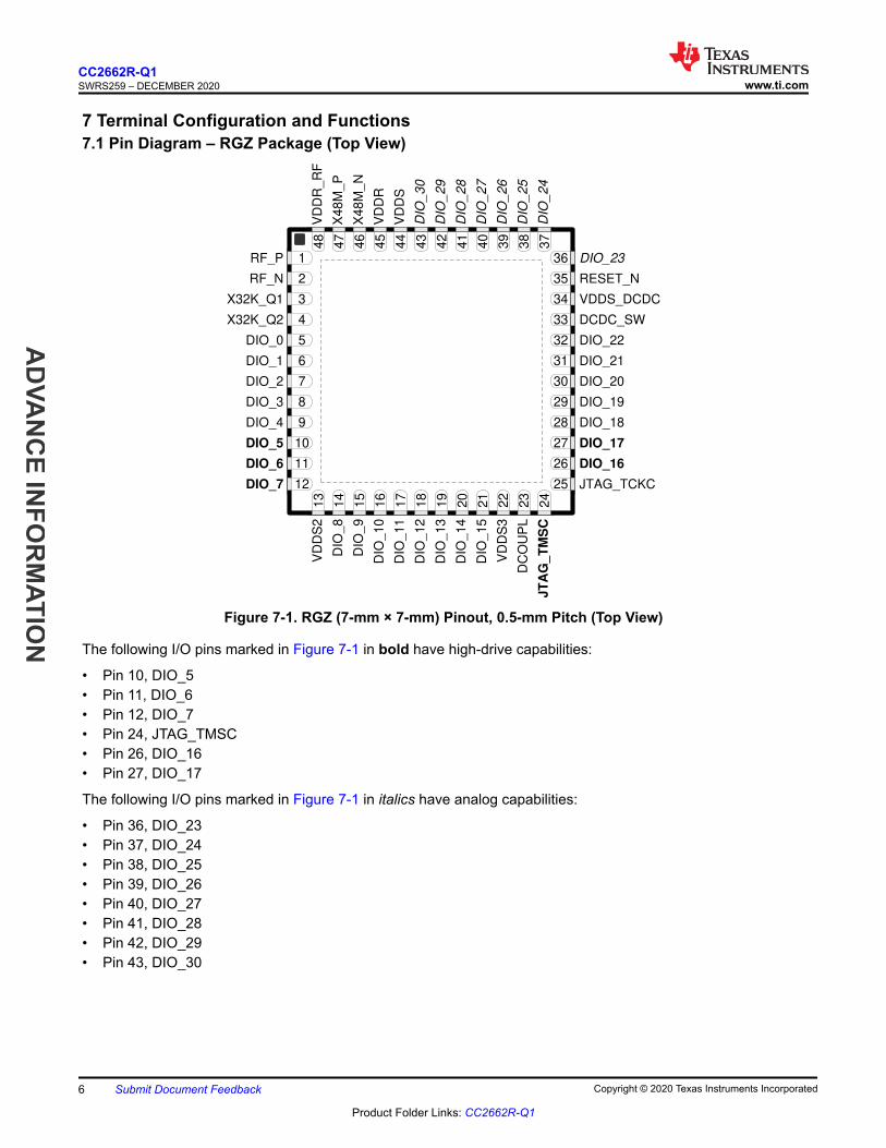
7 Terminal Configuration and Functions7.1 Pin Diagram – RGZ Package (Top View)
40
39
38
37
21
22
23
24
DCDC_SW33
DIO_18
34
RESET_N35
DIO_2336
X32K_Q2 4
X32K_Q1 3
RF_N 2
RF_P 1
DIO_2232
DIO_2131
DIO_2030
DIO_1929
DIO_0 5
DIO_1 6
DIO_2 7
8
28
27
26
JTAG_TCKC25
9
10
11
12
41
42
43
44
20
DIO
_1
5
19
DIO
_1
4
18
17
45
46
47
48
16
15
14
13
DIO_17
DIO_16
VDDS_DCDC
DIO
_1
2
DIO
_1
3
VD
DS
2
DIO
_1
1
DIO
_1
0
DIO_5
DIO_6
DIO_7
DIO_3
DIO_4
DIO
_8
DIO
_9
VD
DS
3
DC
OU
PL
JT
AG
_T
MS
C
DIO
_2
5
DIO
_2
4
VD
DR
VD
DR
_R
F
DIO
_2
6
X4
8M
_P
X4
8M
_N
DIO
_2
8
DIO
_2
9
DIO
_3
0
DIO
_2
7
VD
DS
Figure 7-1. RGZ (7-mm × 7-mm) Pinout, 0.5-mm Pitch (Top View)
The following I/O pins marked in Figure 7-1 in bold have high-drive capabilities:
• Pin 10, DIO_5• Pin 11, DIO_6• Pin 12, DIO_7• Pin 24, JTAG_TMSC• Pin 26, DIO_16• Pin 27, DIO_17
The following I/O pins marked in Figure 7-1 in italics have analog capabilities:
• Pin 36, DIO_23• Pin 37, DIO_24• Pin 38, DIO_25• Pin 39, DIO_26• Pin 40, DIO_27• Pin 41, DIO_28• Pin 42, DIO_29• Pin 43, DIO_30
CC2662R-Q1SWRS259 – DECEMBER 2020 www.ti.com
AD
VAN
CE IN
FOR
MATIO
N
6 Submit Document Feedback Copyright © 2020 Texas Instruments Incorporated
Product Folder Links: CC2662R-Q1

7.2 Signal DescriptionsTable 7-1. Signal Descriptions – RGZ Package
PINI/O TYPE DESCRIPTION
NAME NO.DCDC_SW 33 — Power Output from internal DC/DC converter(1)
DCOUPL 23 — Power 1.27-V regulated digital-supply (decoupling capacitor)(2)
DIO_0 5 I/O Digital GPIO, Sensor Controller
DIO_1 6 I/O Digital GPIO, Sensor Controller
DIO_2 7 I/O Digital GPIO, Sensor Controller
DIO_3 8 I/O Digital GPIO, Sensor Controller
DIO_4 9 I/O Digital GPIO, Sensor Controller
DIO_5 10 I/O Digital GPIO, Sensor Controller, high-drive capability
DIO_6 11 I/O Digital GPIO, Sensor Controller, high-drive capability
DIO_7 12 I/O Digital GPIO, Sensor Controller, high-drive capability
DIO_8 14 I/O Digital GPIO
DIO_9 15 I/O Digital GPIO
DIO_10 16 I/O Digital GPIO
DIO_11 17 I/O Digital GPIO
DIO_12 18 I/O Digital GPIO
DIO_13 19 I/O Digital GPIO
DIO_14 20 I/O Digital GPIO
DIO_15 21 I/O Digital GPIO
DIO_16 26 I/O Digital GPIO, JTAG_TDO, high-drive capability
DIO_17 27 I/O Digital GPIO, JTAG_TDI, high-drive capability
DIO_18 28 I/O Digital GPIO
DIO_19 29 I/O Digital GPIO
DIO_20 30 I/O Digital GPIO
DIO_21 31 I/O Digital GPIO
DIO_22 32 I/O Digital GPIO
DIO_23 36 I/O Digital or Analog GPIO, Sensor Controller, analog
DIO_24 37 I/O Digital or Analog GPIO, Sensor Controller, analog
DIO_25 38 I/O Digital or Analog GPIO, Sensor Controller, analog
DIO_26 39 I/O Digital or Analog GPIO, Sensor Controller, analog
DIO_27 40 I/O Digital or Analog GPIO, Sensor Controller, analog
DIO_28 41 I/O Digital or Analog GPIO, Sensor Controller, analog
DIO_29 42 I/O Digital or Analog GPIO, Sensor Controller, analog
DIO_30 43 I/O Digital or Analog GPIO, Sensor Controller, analog
EGP — — GND Ground – exposed ground pad
JTAG_TMSC 24 I/O Digital JTAG TMSC, high-drive capability
JTAG_TCKC 25 I Digital JTAG TCKC
RESET_N 35 I Digital Reset, active low. No internal pullup resistor
RF_P 1 — RF Positive RF input signal to LNA during RXPositive RF output signal from PA during TX
RF_N 2 — RF Negative RF input signal to LNA during RXNegative RF output signal from PA during TX
VDDR 45 — Power 1.7-V to 1.95-V supply, must be powered from the internal DC/DCconverter or the internal Global LDO(3) (2)
www.ti.comCC2662R-Q1
SWRS259 – DECEMBER 2020
AD
VAN
CE
INFO
RM
ATIO
N
Copyright © 2020 Texas Instruments Incorporated Submit Document Feedback 7
Product Folder Links: CC2662R-Q1
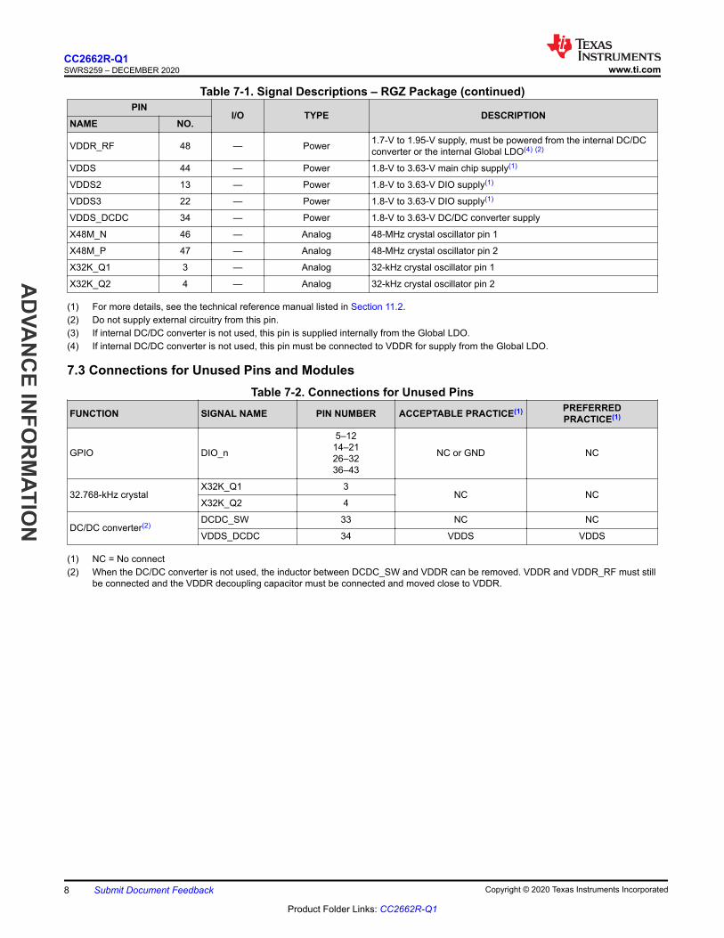
Table 7-1. Signal Descriptions – RGZ Package (continued)PIN
I/O TYPE DESCRIPTIONNAME NO.
VDDR_RF 48 — Power 1.7-V to 1.95-V supply, must be powered from the internal DC/DCconverter or the internal Global LDO(4) (2)
VDDS 44 — Power 1.8-V to 3.63-V main chip supply(1)
VDDS2 13 — Power 1.8-V to 3.63-V DIO supply(1)
VDDS3 22 — Power 1.8-V to 3.63-V DIO supply(1)
VDDS_DCDC 34 — Power 1.8-V to 3.63-V DC/DC converter supply
X48M_N 46 — Analog 48-MHz crystal oscillator pin 1
X48M_P 47 — Analog 48-MHz crystal oscillator pin 2
X32K_Q1 3 — Analog 32-kHz crystal oscillator pin 1
X32K_Q2 4 — Analog 32-kHz crystal oscillator pin 2
(1) For more details, see the technical reference manual listed in Section 11.2.(2) Do not supply external circuitry from this pin.(3) If internal DC/DC converter is not used, this pin is supplied internally from the Global LDO.(4) If internal DC/DC converter is not used, this pin must be connected to VDDR for supply from the Global LDO.
7.3 Connections for Unused Pins and ModulesTable 7-2. Connections for Unused Pins
FUNCTION SIGNAL NAME PIN NUMBER ACCEPTABLE PRACTICE(1) PREFERREDPRACTICE(1)
GPIO DIO_n
5–1214–2126–3236–43
NC or GND NC
32.768-kHz crystalX32K_Q1 3
NC NCX32K_Q2 4
DC/DC converter(2)DCDC_SW 33 NC NC
VDDS_DCDC 34 VDDS VDDS
(1) NC = No connect(2) When the DC/DC converter is not used, the inductor between DCDC_SW and VDDR can be removed. VDDR and VDDR_RF must still
be connected and the VDDR decoupling capacitor must be connected and moved close to VDDR.
CC2662R-Q1SWRS259 – DECEMBER 2020 www.ti.com
AD
VAN
CE IN
FOR
MATIO
N
8 Submit Document Feedback Copyright © 2020 Texas Instruments Incorporated
Product Folder Links: CC2662R-Q1

8 Specifications8.1 Absolute Maximum Ratingsover operating free-air temperature range (unless otherwise noted)(1) (2)
MIN MAX UNITVDDS(3) Supply voltage –0.3 4.1 V
Voltage on any digital pin (4) (5) –0.3 VDDS + 0.3, max 4.1 V
Voltage on crystal oscillator pins, X32K_Q1, X32K_Q2, X48M_N and X48M_P –0.3 VDDR + 0.3, max 2.25 V
Vin Voltage on ADC input
Voltage scaling enabled –0.3 VDDS
VVoltage scaling disabled, internal reference –0.3 1.49
Voltage scaling disabled, VDDS as reference –0.3 VDDS / 2.9
Tstg Storage temperature –40 150 °C
(1) Stresses beyond those listed under Absolute Maximum Ratings may cause permanent damage to the device. These are stress ratingsonly, and functional operation of the device at these or any other conditions beyond those indicated under Recommended OperatingConditions is not implied. Exposure to absolute-maximum-rated conditions for extended periods may affect device reliability.
(2) All voltage values are with respect to ground, unless otherwise noted.(3) VDDS2 and VDDS3 must be at the same potential as VDDS.(4) Including analog capable DIO.(5) Injection current is not supported on any GPIO pin
8.2 ESD RatingsVALUE UNIT
VESDElectrostaticdischarge
Human body model (HBM), per AEC Q100-002(1) (2) All pins ±2000 V
Charged device model (CDM), per AEC Q100-011(3) All pins ±500 V
(1) AEC Q100-002 indicates HBM stressing is done in accordance with the ANSI/ESDA/JEDEC JS-001 specification.(2) JEDEC document JEP155 states that 500-V HBM allows safe manufacturing with a standard ESD control process(3) JEDEC document JEP157 states that 250-V CDM allows safe manufacturing with a standard ESD control process
8.3 Recommended Operating Conditionsover operating free-air temperature range (unless otherwise noted)
MIN MAX UNITOperating ambient temperature range –40 105 °C
Operating supply voltage (VDDS) 1.8 3.63 V
Rising supply voltage slew rate 0 100 mV/µs
Falling supply voltage slew rate(1) 0 20 mV/µs
(1) For small coin-cell batteries, with high worst-case end-of-life equivalent source resistance, a 22-µF VDDS input capacitor must be usedto ensure compliance with this slew rate.
8.4 Power Supply and Modulesover operating free-air temperature range (unless otherwise noted)
PARAMETER TYP UNITVDDS Power-on-Reset (POR) threshold 1.1 - 1.55 V
VDDS Brown-out Detector (BOD) Rising threshold 1.77 V
VDDS Brown-out Detector (BOD), before initial boot (1) Rising threshold 1.70 V
VDDS Brown-out Detector (BOD) Falling threshold 1.75 V
(1) Brown-out Detector is trimmed at initial boot, value is kept until device is reset by a POR reset or the RESET_N pin
www.ti.comCC2662R-Q1
SWRS259 – DECEMBER 2020
AD
VAN
CE
INFO
RM
ATIO
N
Copyright © 2020 Texas Instruments Incorporated Submit Document Feedback 9
Product Folder Links: CC2662R-Q1

8.5 Power Consumption - Power ModesWhen measured on the CC26x2REM-7ID-Q1 reference design with Tc = 25 °C, VDDS = 3.0 V with DC/DC enabled unlessotherwise noted.
PARAMETER TEST CONDITIONS TYP UNITCore Current Consumption
Icore
Reset and ShutdownReset. RESET_N pin asserted or VDDS below power-on-resetthreshold 150
nAShutdown. No clocks running, no retention 150
Standbywithout cacheretention
RTC running, CPU, 80KB RAM and (partial) register retention.RCOSC_LF 0.94 µA
RTC running, CPU, 80KB RAM and (partial) register retentionXOSC_LF 1.09 µA
Standbywith cache retention
RTC running, CPU, 80KB RAM and (partial) register retention.RCOSC_LF 3.2 µA
RTC running, CPU, 80KB RAM and (partial) register retention.XOSC_LF 3.3 µA
Idle Supply Systems and RAM poweredRCOSC_HF 675 µA
Active MCU running CoreMark at 48 MHzRCOSC_HF 3.39 mA
Peripheral Current Consumption
Iperi
Peripheral powerdomain Delta current with domain enabled 97.7
µA
Serial power domain Delta current with domain enabled 7.2
RF Core Delta current with power domain enabled,clock enabled, RF Core idle 210.9
µDMA Delta current with clock enabled, module is idle 63.9
Timers Delta current with clock enabled, module is idle(3) 81.0
I2C Delta current with clock enabled, module is idle 10.8
I2S Delta current with clock enabled, module is idle 27.6
SSI Delta current with clock enabled, module is idle 82.9
UART Delta current with clock enabled, module is idle(1) 167.5
CRYPTO (AES) Delta current with clock enabled, module is idle(2) 25.6
PKA Delta current with clock enabled, module is idle 84.7
TRNG Delta current with clock enabled, module is idle 35.6
Sensor Controller Engine Consumption
ISCEActive mode 24 MHz, infinite loop 808.5
µALow-power mode 2 MHz, infinite loop 31.9
(1) Only one UART running(2) Only one SSI running(3) Only one GPTimer running
CC2662R-Q1SWRS259 – DECEMBER 2020 www.ti.com
AD
VAN
CE IN
FOR
MATIO
N
10 Submit Document Feedback Copyright © 2020 Texas Instruments Incorporated
Product Folder Links: CC2662R-Q1

8.6 Power Consumption - Radio ModesWhen measured on the CC26x2REM-7ID-Q1 reference design with Tc = 25 °C, VDDS = 3.0 V with DC/DC enabled unlessotherwise noted.
PARAMETER TEST CONDITIONS TYP UNITRadio receive current 2440 MHz 6.9 mA
Radio transmit current
0 dBm output power setting2440 MHz 7.3 mA
+5 dBm output power setting2440 MHz 9.6 mA
8.7 Nonvolatile (Flash) Memory CharacteristicsOver operating free-air temperature range and VDDS = 3.0 V (unless otherwise noted)
PARAMETER TEST CONDITIONS MIN TYP MAX UNITFlash sector size 8 KB
Supported flash erase cycles before failure, full bank(1) 30 k Cycles
Supported flash erase cycles before failure, singlesector(2) 60 k Cycles
Maximum number of write operations per row beforesector erase(3) 83 Write
Operations
Flash retention 105 °C 11.4 Years at105 °C
Flash sector erase current Average delta current 10.7 mA
Flash sector erase time(4) Zero cycles 10 ms
Flash sector erase time(4) 30k cycles 4000 ms
Flash write current Average delta current, 4 bytes at a time 6.2 mA
Flash write time 4 bytes at a time 21.6 µs
(1) A full bank erase is counted as a single erase cycle on each sector(2) Up to 4 customer-designated sectors can be individually erased an additional 30k times beyond the baseline bank limitation of 30k
cycles(3) Each wordline is 2048 bits (or 256 bytes) wide. This limitation corresponds to sequential memory writes of 4 (3.1) bytes minimum per
write over a whole wordline. If additional writes to the same wordline are required, a sector erase is required once the maximumnumber of write operations per row is reached.
(4) This number is dependent on Flash aging and increases over time and erase cycles
8.8 Thermal Resistance Characteristics
THERMAL METRIC(1)
PACKAGE
UNITRTC(VQFN)48 PINS
RθJA Junction-to-ambient thermal resistance 23.0 °C/W(2)
RθJC(top) Junction-to-case (top) thermal resistance 13.2 °C/W(2)
RθJB Junction-to-board thermal resistance 7.5 °C/W(2)
ψJT Junction-to-top characterization parameter 0.3 °C/W(2)
ψJB Junction-to-board characterization parameter 7.4 °C/W(2)
RθJC(bot) Junction-to-case (bottom) thermal resistance 1.3 °C/W(2)
(1) For more information about traditional and new thermal metrics, see Semiconductor and IC Package Thermal Metrics.(2) °C/W = degrees Celsius per watt.
www.ti.comCC2662R-Q1
SWRS259 – DECEMBER 2020
AD
VAN
CE
INFO
RM
ATIO
N
Copyright © 2020 Texas Instruments Incorporated Submit Document Feedback 11
Product Folder Links: CC2662R-Q1

8.9 Proprietary WBMS - Receive (RX)When measured on the CC26x2REM-7ID-Q1 reference design with Tc = 25 °C, VDDS = 3.0 V, fRF = 2440 MHz with DC/DCenabled unless otherwise noted. All measurements are performed at the antenna input with a combined RX and TX path.All measurements are performed conducted.
PARAMETER TEST CONDITIONS MIN TYP MAX UNIT2 Mbps
Receiver sensitivity Differential mode. Measured at SMA connector,BER = 10–3 –92 dBm
Receiver saturation Differential mode. Measured at SMA connector,BER = 10–3 > 5 dBm
Frequency error toleranceDifference between the incoming carrierfrequency and the internally generated carrierfrequency
> (–440 / 500) kHz
Data rate error tolerance Difference between incoming data rate and theinternally generated data rate (37-byte packets) > (–700 / 750) ppm
Co-channel rejection(1) Wanted signal at –67 dBm, modulated interferer inchannel, BER = 10–3 –7 dB
Selectivity, ±2 MHz(1)Wanted signal at –67 dBm, modulated interferer at±2 MHz, Image frequency is at –2 MHz, BER =10–3
8 / 4(2) dB
Selectivity, ±4 MHz(1) Wanted signal at –67 dBm, modulated interferer at±4 MHz, BER = 10–3 36 / 34(2) dB
Selectivity, ±6 MHz or more(1) Wanted signal at –67 dBm, modulated interferer at±6 MHz or more, BER = 10–3 37 / 36(2) dB
Selectivity, image frequency(1) Wanted signal at –67 dBm, modulated interferer atimage frequency, BER = 10–3 4 dB
Selectivity, image frequency±2 MHz(1)
Note that Image frequency + 2 MHz is the Co-channel. Wanted signal at –67 dBm, modulatedinterferer at ±2 MHz from image frequency, BER =10–3
–7 / 36(2) dB
Out-of-band blocking(3) 30 MHz to 2000 MHz –16 dBm
Out-of-band blocking 2003 MHz to 2399 MHz –21 dBm
Out-of-band blocking 2484 MHz to 2997 MHz –15 dBm
Out-of-band blocking 3000 MHz to 12.75 GHz –12 dBm
IntermodulationWanted signal at 2402 MHz, –64 dBm. Twointerferers at 2405 and 2408 MHz respectively, atthe given power level
–38 dBm
RSSI dynamic range 63 dB
RSSI Accuracy (+/-) ±4 dB
(1) Numbers given as I/C dB(2) X / Y, where X is +N MHz and Y is –N MHz(3) Excluding one exception at Fwanted / 2
CC2662R-Q1SWRS259 – DECEMBER 2020 www.ti.com
AD
VAN
CE IN
FOR
MATIO
N
12 Submit Document Feedback Copyright © 2020 Texas Instruments Incorporated
Product Folder Links: CC2662R-Q1

8.10 Proprietary WBMS - Transmit (TX)All measurements are performed conducted.
PARAMETER TEST CONDITIONS MIN TYP MAX UNITGeneral Parameters5dBm output power Differential mode, delivered to a single-ended 50 Ω load through a balun 5 dBm
Output powerprogrammablerange
Differential mode, delivered to a single-ended 50 Ω load through a balun 26 dB
Spurious emissions and harmonics
Spurious emissions(1)
f < 1 GHz, outside restrictedbands +5 dBm setting < –36 dBm
f < 1 GHz, restricted bandsETSI +5 dBm setting < –54 dBm
f < 1 GHz, restricted bandsFCC +5 dBm setting < –55 dBm
f > 1 GHz, including harmonics +5 dBm setting < –42 dBm
Harmonics (1)Second harmonic +5 dBm setting < –42 dBm
Third harmonic +5 dBm setting < –42 dBm
(1) Suitable for systems targeting compliance with worldwide radio-frequency regulations ETSI EN 300 328 and EN 300 440 Category 2(Europe), FCC CFR47 Part 15 (US), and ARIB STD-T66 (Japan).
8.11 Timing and Switching Characteristics8.11.1 Reset Timing
PARAMETER MIN TYP MAX UNITRESET_N low duration 1 µs
8.11.2 Wakeup TimingMeasured over operating free-air temperature with VDDS = 3.0 V (unless otherwise noted). The times listed here do notinclude software overhead.
PARAMETER TEST CONDITIONS MIN TYP MAX UNITMCU, Reset to Active(1) 850 - 3000 µs
MCU, Shutdown to Active(1) 850 - 3000 µs
MCU, Standby to Active 160 µs
MCU, Active to Standby 36 µs
MCU, Idle to Active 14 µs
(1) The wakeup time is dependent on remaining charge on the VDDR capacitor when starting the device, and thus how long the devicehas been in Reset or Shutdown before starting up again.
www.ti.comCC2662R-Q1
SWRS259 – DECEMBER 2020
AD
VAN
CE
INFO
RM
ATIO
N
Copyright © 2020 Texas Instruments Incorporated Submit Document Feedback 13
Product Folder Links: CC2662R-Q1

8.11.3 Clock Specifications8.11.3.1 48 MHz Crystal Oscillator (XOSC_HF)Measured on the CC26x2REM-7ID-Q1 reference design with Tc = 25 °C, VDDS = 3.0 V, unless otherwise noted.(1)
PARAMETER MIN TYP MAX UNITCrystal frequency 48 MHz
ESR Equivalent series resistance6 pF < CL ≤ 9 pF 20 60 Ω
ESR Equivalent series resistance5 pF < CL ≤ 6 pF 80 Ω
LMMotional inductance, relates to the load capacitance that is used for thecrystal (CL in Farads)(5) < 0.3 × 10⁻²⁴ / CL 2 H
CL Crystal load capacitance(4) 5 7(3) 9 pF
Start-up time(2) 200 µs
(1) Probing or otherwise stopping the crystal while the DC/DC converter is enabled may cause permanent damage to the device.(2) Start-up time using the TI-provided power driver. Start-up time may increase if driver is not used.(3) On-chip default connected capacitance including reference design parasitic capacitance. Connected internal capacitance is changed
through software in the Customer Configuration section (CCFG).(4) Adjustable load capacitance is integrated within the device.(5) The crystal manufacturer's specification must satisfy this requirement for proper operation.
8.11.3.2 48 MHz RC Oscillator (RCOSC_HF)Measured on the CC26x2REM-7ID-Q1 reference design with Tc = 25 °C, VDDS = 3.0 V, unless otherwise noted.
MIN TYP MAX UNITFrequency 48 MHz
Uncalibrated frequency accuracy ±1 %
Calibrated frequency accuracy(1) ±0.25 %
Start-up time 5 µs
(1) Accuracy relative to the calibration source (XOSC_HF)
8.11.3.3 2 MHz RC Oscillator (RCOSC_MF)Measured on the CC26x2REM-7ID-Q1 reference design with Tc = 25 °C, VDDS = 3.0 V, unless otherwise noted.
MIN TYP MAX UNITCalibrated frequency 2 MHz
Start-up time 5 µs
8.11.3.4 32.768 kHz Crystal Oscillator (XOSC_LF)Measured on the CC26x2REM-7ID-Q1 reference design with Tc = 25 °C, VDDS = 3.0 V, unless otherwise noted.
MIN TYP MAX UNITCrystal frequency 32.768 kHz
ESR Equivalent series resistance 30 100 kΩ
CL Crystal load capacitance 6 7(1) 12 pF
(1) Default load capacitance using TI reference designs including parasitic capacitance. Crystals with different load capacitance may beused.
CC2662R-Q1SWRS259 – DECEMBER 2020 www.ti.com
AD
VAN
CE IN
FOR
MATIO
N
14 Submit Document Feedback Copyright © 2020 Texas Instruments Incorporated
Product Folder Links: CC2662R-Q1

8.11.3.5 32 kHz RC Oscillator (RCOSC_LF)Measured on the CC26x2REM-7ID-Q1 reference design with Tc = 25 °C, VDDS = 3.0 V, unless otherwise noted.
MIN TYP MAX UNITCalibrated frequency 32.8 (1) kHz
Temperature coefficient ±50 ppm/C
(1) When using RCOSC_LF as source for the low frequency system clock (SCLK_LF), the accuracy of the SCLK_LF-derived Real TimeClock (RTC) can be improved by measuring RCOSC_LF relative to XOSC_HF and compensating for the RTC tick speed. Thisfunctionality is available through the TI-provided Power driver.
www.ti.comCC2662R-Q1
SWRS259 – DECEMBER 2020
AD
VAN
CE
INFO
RM
ATIO
N
Copyright © 2020 Texas Instruments Incorporated Submit Document Feedback 15
Product Folder Links: CC2662R-Q1

8.11.4 Synchronous Serial Interface (SSI) Characteristics8.11.4.1 Synchronous Serial Interface (SSI) CharacteristicsOver operating free-air temperature range (unless otherwise noted)
PARAMETERNO. PARAMETER MIN TYP MAX UNIT
S1 tclk_per SSIClk cycle time 12 65024 System Clocks (2)
S2(1) tclk_high SSIClk high time 0.5 tclk_per
S3(1) tclk_low SSIClk low time 0.5 tclk_per
(1) Refer to SSI timing diagrams Figure 8-1, Figure 8-2, and Figure 8-3.(2) When using the TI-provided Power driver, the SSI system clock is always 48 MHz.
SSIClk
SSIFss
SSITx
SSIRxMSB LSB
S2
S3
S1
4 to 16 bits
Figure 8-1. SSI Timing for TI Frame Format (FRF = 01), Single Transfer Timing Measurement
0
SSIClk
SSIFss
SSITx
SSIRx
MSB LSB
MSB LSB
S2
S3
S1
8-bit control
4 to 16 bits output data
Figure 8-2. SSI Timing for MICROWIRE Frame Format (FRF = 10), Single Transfer
CC2662R-Q1SWRS259 – DECEMBER 2020 www.ti.com
AD
VAN
CE IN
FOR
MATIO
N
16 Submit Document Feedback Copyright © 2020 Texas Instruments Incorporated
Product Folder Links: CC2662R-Q1

SSIClk(SPO = 1)
SSITx(Master)
SSIRx(Slave) LSB
SSIClk(SPO = 0)
S2
S1
SSIFss
LSB
S3
MSB
MSB
Figure 8-3. SSI Timing for SPI Frame Format (FRF = 00), With SPH = 1
8.11.5 UART8.11.5.1 UART CharacteristicsOver operating free-air temperature range (unless otherwise noted)
PARAMETER MIN TYP MAX UNITUART rate 3 MBaud
www.ti.comCC2662R-Q1
SWRS259 – DECEMBER 2020
AD
VAN
CE
INFO
RM
ATIO
N
Copyright © 2020 Texas Instruments Incorporated Submit Document Feedback 17
Product Folder Links: CC2662R-Q1

8.12 Peripheral Characteristics8.12.1 ADC8.12.1.1 Analog-to-Digital Converter (ADC) CharacteristicsTc = 25 °C, VDDS = 3.0 V and voltage scaling enabled, unless otherwise noted.(1)
Performance numbers require use of offset and gain adjustements in software by TI-provided ADC drivers.PARAMETER TEST CONDITIONS MIN TYP MAX UNIT
Input voltage range 0 VDDS V
Resolution 12 Bits
Sample rate 200 kSamples/s
Offset Internal 4.3 V equivalent reference(2) –0.24 LSB
Gain error Internal 4.3 V equivalent reference(2) 7.14 LSB
DNL(4) Differential nonlinearity >–1 LSB
INL Integral nonlinearity ±4 LSB
ENOB Effective number of bits
Internal 4.3 V equivalent reference(2), 200 kSamples/s,9.6 kHz input tone 9.8
Bits
Internal 4.3 V equivalent reference(2), 200 kSamples/s,9.6 kHz input tone, DC/DC enabled 9.8
VDDS as reference, 200 kSamples/s, 9.6 kHz inputtone 10.1
Internal reference, voltage scaling disabled,32 samples average, 200 kSamples/s, 300 Hz inputtone
11.1
Internal reference, voltage scaling disabled,14-bit mode, 200 kSamples/s, 600 Hz input tone (5) 11.3
Internal reference, voltage scaling disabled,15-bit mode, 200 kSamples/s, 150 Hz input tone (5) 11.6
THD Total harmonic distortion
Internal 4.3 V equivalent reference(2), 200 kSamples/s,9.6 kHz input tone –65
dBVDDS as reference, 200 kSamples/s, 9.6 kHz inputtone –70
Internal reference, voltage scaling disabled,32 samples average, 200 kSamples/s, 300 Hz inputtone
–72
SINAD,SNDR
Signal-to-noiseanddistortion ratio
Internal 4.3 V equivalent reference(2), 200 kSamples/s,9.6 kHz input tone 60
dBVDDS as reference, 200 kSamples/s, 9.6 kHz inputtone 63
Internal reference, voltage scaling disabled,32 samples average, 200 kSamples/s, 300 Hz inputtone
68
SFDR Spurious-free dynamicrange
Internal 4.3 V equivalent reference(2), 200 kSamples/s,9.6 kHz input tone 70
dBVDDS as reference, 200 kSamples/s, 9.6 kHz inputtone 73
Internal reference, voltage scaling disabled,32 samples average, 200 kSamples/s, 300 Hz inputtone
75
Conversion time Serial conversion, time-to-output, 24 MHz clock 50 clock-cycles
Current consumption Internal 4.3 V equivalent reference(2) 0.42 mA
Current consumption VDDS as reference 0.6 mA
CC2662R-Q1SWRS259 – DECEMBER 2020 www.ti.com
AD
VAN
CE IN
FOR
MATIO
N
18 Submit Document Feedback Copyright © 2020 Texas Instruments Incorporated
Product Folder Links: CC2662R-Q1
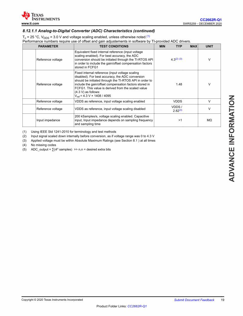
8.12.1.1 Analog-to-Digital Converter (ADC) Characteristics (continued)Tc = 25 °C, VDDS = 3.0 V and voltage scaling enabled, unless otherwise noted.(1)
Performance numbers require use of offset and gain adjustements in software by TI-provided ADC drivers.PARAMETER TEST CONDITIONS MIN TYP MAX UNIT
Reference voltage
Equivalent fixed internal reference (input voltagescaling enabled). For best accuracy, the ADCconversion should be initiated through the TI-RTOS APIin order to include the gain/offset compensation factorsstored in FCFG1
4.3(2) (3) V
Reference voltage
Fixed internal reference (input voltage scalingdisabled). For best accuracy, the ADC conversionshould be initiated through the TI-RTOS API in order toinclude the gain/offset compensation factors stored inFCFG1. This value is derived from the scaled value(4.3 V) as follows:Vref = 4.3 V × 1408 / 4095
1.48 V
Reference voltage VDDS as reference, input voltage scaling enabled VDDS V
Reference voltage VDDS as reference, input voltage scaling disabled VDDS /2.82(3) V
Input impedance200 kSamples/s, voltage scaling enabled. Capacitiveinput, Input impedance depends on sampling frequencyand sampling time
>1 MΩ
(1) Using IEEE Std 1241-2010 for terminology and test methods(2) Input signal scaled down internally before conversion, as if voltage range was 0 to 4.3 V(3) Applied voltage must be within Absolute Maximum Ratings (see Section 8.1 ) at all times(4) No missing codes(5) ADC_output = ∑(4n samples) >> n,n = desired extra bits
www.ti.comCC2662R-Q1
SWRS259 – DECEMBER 2020
AD
VAN
CE
INFO
RM
ATIO
N
Copyright © 2020 Texas Instruments Incorporated Submit Document Feedback 19
Product Folder Links: CC2662R-Q1

8.12.2 DAC8.12.2.1 Digital-to-Analog Converter (DAC) CharacteristicsTc = 25 °C, VDDS = 3.0 V, unless otherwise noted.
PARAMETER TEST CONDITIONS MIN TYP MAX UNITGeneral Parameters
Resolution 8 Bits
VDDS Supply voltageAny load, any VREF, pre-charge OFF, DAC charge-pump ON 1.8 3.63
VAny load, VREF = DCOUPL, pre-charge ON 2.6 3.63
FDAC Clock frequency Buffer OFF (internal load) 16 1000 kHz
Voltage output settlingtime VREF = VDDS, buffer OFF, internal load 13 1 / FDAC
Internal Load - Continuous Time Comparator / Low Power Clocked Comparator
DNL
Differential nonlinearity
VREF = VDDS,load = Continuous Time Comparator or Low PowerClocked ComparatorFDAC = 250 kHz
±1
LSB(1)
Differential nonlinearity
VREF = VDDS,load = Continuous Time Comparator or Low PowerClocked ComparatorFDAC = 16 kHz
±1.2
Offset error(2)
Load = Continuous TimeComparator
VREF = VDDS= 3.63 V ±0.67
LSB(1)
VREF = VDDS= 3.0 V ±0.81
VREF = VDDS = 1.8 V ±1.27
VREF = DCOUPL, pre-charge ON ±3.43
VREF = DCOUPL, pre-charge OFF ±2.88
Offset error(2)
Load = Low PowerClocked Comparator
VREF = VDDS = 3.63 V ±0.77
LSB(1)
VREF = VDDS = 3.0 V ±0.77
VREF = VDDS= 1.8 V ±3.46
VREF = DCOUPL, pre-charge ON ±3.44
VREF = DCOUPL, pre-charge OFF ±4.70
Max code output voltagevariation(2)
Load = Continuous TimeComparator
VREF = VDDS = 3.63 V ±1.61
LSB(1)
VREF = VDDS = 3.0 V ±1.71
VREF = VDDS= 1.8 V ±2.10
VREF = DCOUPL, pre-charge ON ±6.00
VREF = DCOUPL, pre-charge OFF ±3.85
Max code output voltagevariation(2)
Load = Low PowerClocked Comparator
VREF =VDDS= 3.63 V ±2.92
LSB(1)
VREF =VDDS= 3.0 V ±3.06
VREF = VDDS= 1.8 V ±3.91
VREF = DCOUPL, pre-charge ON ±7.84
VREF = DCOUPL, pre-charge OFF ±4.06
CC2662R-Q1SWRS259 – DECEMBER 2020 www.ti.com
AD
VAN
CE IN
FOR
MATIO
N
20 Submit Document Feedback Copyright © 2020 Texas Instruments Incorporated
Product Folder Links: CC2662R-Q1

8.12.2.1 Digital-to-Analog Converter (DAC) Characteristics (continued)Tc = 25 °C, VDDS = 3.0 V, unless otherwise noted.
PARAMETER TEST CONDITIONS MIN TYP MAX UNIT
Output voltage range(2)
Load = Continuous TimeComparator
VREF = VDDS= 3.63 V, code 1 0.03
V
VREF = VDDS= 3.63 V, code 255 3.46
VREF = VDDS= 3.0 V, code 1 0.02
VREF = VDDS= 3.0 V, code 255 2.86
VREF = VDDS= 1.8 V, code 1 0.01
VREF = VDDS = 1.8 V, code 255 1.71
VREF = DCOUPL, pre-charge OFF, code 1 0.01
VREF = DCOUPL, pre-charge OFF, code 255 1.21
VREF = DCOUPL, pre-charge ON, code 1 1.27
VREF = DCOUPL, pre-charge ON, code 255 2.46
Output voltage range(2)
Load = Low PowerClocked Comparator
VREF = VDDS= 3.63 V, code 1 0.03
V
VREF = VDDS= 3.63 V, code 255 3.46
VREF = VDDS= 3.0 V, code 1 0.02
VREF = VDDS= 3.0 V, code 255 2.85
VREF = VDDS = 1.8 V, code 1 0.01
VREF = VDDS = 1.8 V, code 255 1.71
VREF = DCOUPL, pre-charge OFF, code 1 0.01
VREF = DCOUPL, pre-charge OFF, code 255 1.21
VREF = DCOUPL, pre-charge ON, code 1 1.27
VREF = DCOUPL, pre-charge ON, code 255 2.46
(1) 1 LSB (VREF 3.63 V/3.0 V/1.8 V/DCOUPL/ADCREF) = 13.44 mV/11.13 mV/6.68 mV/4.67 mV/5.48 mV(2) Includes comparator offset
www.ti.comCC2662R-Q1
SWRS259 – DECEMBER 2020
AD
VAN
CE
INFO
RM
ATIO
N
Copyright © 2020 Texas Instruments Incorporated Submit Document Feedback 21
Product Folder Links: CC2662R-Q1

8.12.3 Temperature and Battery Monitor8.12.3.1 Temperature SensorMeasured on the CC26x2REM-7ID-Q1 reference design with Tc = 25 °C, VDDS = 3.0 V, unless otherwise noted.
PARAMETER TEST CONDITIONS MIN TYP MAX UNITResolution 2 °C
Accuracy -40 °C to 0 °C ±4.0 °C
Accuracy 0 °C to 105 °C ±2.5 °C
Supply voltage coefficient(1) 3.6 °C/V
(1) The temperature sensor is automatically compensated for VDDS variation when using the TI-provided driver.
8.12.3.2 Battery MonitorMeasured on the CC26x2REM-7ID-Q1 reference design with Tc = 25 °C, unless otherwise noted.
PARAMETER TEST CONDITIONS MIN TYP MAX UNITResolution 25 mV
Range 1.8 3.63 V
Integral nonlinearity (max) 28 72 mV
Accuracy VDDS = 3.0 V 22.5 mV
Offset error -32 mV
Gain error -1.3 %
CC2662R-Q1SWRS259 – DECEMBER 2020 www.ti.com
AD
VAN
CE IN
FOR
MATIO
N
22 Submit Document Feedback Copyright © 2020 Texas Instruments Incorporated
Product Folder Links: CC2662R-Q1

8.12.4 Comparators8.12.4.1 Continuous Time ComparatorTc = 25°C, VDDS = 3.0 V, unless otherwise noted.
PARAMETER TEST CONDITIONS MIN TYP MAX UNITInput voltage range(1) 0 VDDS V
Offset Measured at VDDS / 2 ±5 mV
Decision time Step from –10 mV to 10 mV 0.78 µs
Current consumption Internal reference 8.6 µA
(1) The input voltages can be generated externally and connected throughout I/Os or an internal reference voltage can be generated usingthe DAC
8.12.4.2 Low-Power Clocked ComparatorTc = 25 °C, VDDS = 3.0 V, unless otherwise noted.
PARAMETER TEST CONDITIONS MIN TYP MAX UNITInput voltage range 0 VDDS V
Clock frequency SCLK_LF
Internal reference voltage(1) Using internal DAC with VDDS as referencevoltage, DAC code = 0 - 255
0.024 -2.865 V
Offset Measured at VDDS / 2, includes error frominternal DAC ±5 mV
Decision time Step from –50 mV to 50 mV 1 ClockCycle
(1) The comparator can use an internal 8 bits DAC as its reference. The DAC output voltage range depends on the reference voltageselected. See Section 8.12.2.1
8.12.5 Current Source8.12.5.1 Programmable Current SourceTc = 25 °C, VDDS = 3.0 V, unless otherwise noted.
PARAMETER TEST CONDITIONS MIN TYP MAX UNITCurrent source programmable output range(logarithmic range) 0.25 - 20 µA
Resolution 0.25 µA
www.ti.comCC2662R-Q1
SWRS259 – DECEMBER 2020
AD
VAN
CE
INFO
RM
ATIO
N
Copyright © 2020 Texas Instruments Incorporated Submit Document Feedback 23
Product Folder Links: CC2662R-Q1

8.12.6 GPIO8.12.6.1 GPIO DC Characteristics
PARAMETER TEST CONDITIONS MIN TYP MAX UNITTA = 25 °C, VDDS = 1.8 VGPIO VOH at 8 mA load IOCURR = 2, high-drive GPIOs only 1.44 V
GPIO VOL at 8 mA load IOCURR = 2, high-drive GPIOs only 0.36 V
GPIO VOH at 4 mA load IOCURR = 1 1.44 V
GPIO VOL at 4 mA load IOCURR = 1 0.36 V
GPIO pullup current Input mode, pullup enabled, Vpad = 0 V 32 68 110 µA
GPIO pulldown current Input mode, pulldown enabled, Vpad = VDDS 11 18.5 39 µA
GPIO low-to-high input transition, with hysteresis IH = 1, transition voltage for input read as 0 →1 0.72 1.08 1.17 V
GPIO high-to-low input transition, with hysteresis IH = 1, transition voltage for input read as 1 →0 0.54 0.72 0.87 V
GPIO input hysteresis IH = 1, difference between 0 → 1and 1 → 0 points 0.18 0.36 0.51 V
GPIO minimum VIH Lowest GPIO input voltage reliably interpretedas High 1.17 V
GPIO maximum VIL Highest GPIO Input voltage reliably interpretedas Low 0.63 V
TA = 25 °C, VDDS = 3.0 VGPIO VOH at 8 mA load IOCURR = 2, high-drive GPIOs only 2.4 V
GPIO VOL at 8 mA load IOCURR = 2, high-drive GPIOs only 0.6 V
GPIO VOH at 4 mA load IOCURR = 1 2.4 V
GPIO VOL at 4 mA load IOCURR = 1 0.6 V
TA = 25 °C, VDDS = 3.63 VGPIO VOH at 8 mA load IOCURR = 2, high-drive GPIOs only 2.9 V
GPIO VOL at 8 mA load IOCURR = 2, high-drive GPIOs only 0.6 V
GPIO VOH at 4 mA load IOCURR = 1 2.9 V
GPIO VOL at 4 mA load IOCURR = 1 0.6 V
GPIO pullup current Input mode, pullup enabled, Vpad = 0 V 135 264 380 µA
GPIO pulldown current Input mode, pulldown enabled, Vpad = VDDS 64 102 178 µA
GPIO low-to-high input transition, with hysteresis IH = 1, transition voltage for input read as 0 →1 1.52 1.90 2.21 V
GPIO high-to-low input transition, with hysteresis IH = 1, transition voltage for input read as 1 →0 1.14 1.48 1.83 V
GPIO input hysteresis IH = 1, difference between 0 → 1and 1 → 0 points 0.38 0.42 1.07 V
GPIO minimum VIH Lowest GPIO input voltage reliably interpretedas a High 2.47 V
GPIO maximum VIL Highest GPIO input voltage reliably interpretedas a Low 1.33 V
CC2662R-Q1SWRS259 – DECEMBER 2020 www.ti.com
AD
VAN
CE IN
FOR
MATIO
N
24 Submit Document Feedback Copyright © 2020 Texas Instruments Incorporated
Product Folder Links: CC2662R-Q1

9 Detailed Description9.1 OverviewFigure 4-1 shows the core modules of the CC2662R-Q1 device.
9.2 System CPUThe CC2662R-Q1 SimpleLink™ Wireless MCU contains an Arm® Cortex®-M4F system CPU, which runs theapplication and the higher layers of the Wireless BMS protocol stack.
The system CPU is the foundation of a high-performance, low-cost platform that meets the system requirementsof minimal memory implementation, and low-power consumption, while delivering outstanding computationalperformance and exceptional system response to interrupts.
Its features include the following:• ARMv7-M architecture optimized for small-footprint embedded applications• Arm Thumb®-2 mixed 16- and 32-bit instruction set delivers the high performance expected of a 32-bit Arm
core in a compact memory size• Fast code execution permits increased sleep mode time• Deterministic, high-performance interrupt handling for time-critical applications• Single-cycle multiply instruction and hardware divide• Hardware division and fast digital-signal-processing oriented multiply accumulate• Saturating arithmetic for signal processing• IEEE 754-compliant single-precision Floating Point Unit (FPU)• Memory Protection Unit (MPU) for safety-critical applications• Full debug with data matching for watchpoint generation
– Data Watchpoint and Trace Unit (DWT)– JTAG Debug Access Port (DAP)– Flash Patch and Breakpoint Unit (FPB)
• Trace support reduces the number of pins required for debugging and tracing– Instrumentation Trace Macrocell Unit (ITM)– Trace Port Interface Unit (TPIU) with asynchronous serial wire output (SWO)
• Optimized for single-cycle flash memory access• Tightly connected to 8-KB 4-way random replacement cache for minimal active power consumption and wait
states• Ultra-low-power consumption with integrated sleep modes• 48 MHz operation• 1.25 DMIPS per MHz
www.ti.comCC2662R-Q1
SWRS259 – DECEMBER 2020
AD
VAN
CE
INFO
RM
ATIO
N
Copyright © 2020 Texas Instruments Incorporated Submit Document Feedback 25
Product Folder Links: CC2662R-Q1

9.3 Radio (RF Core)The RF Core is a highly flexible and future proof radio module which contains an Arm Cortex-M0 processor thatinterfaces the analog RF and base-band circuitry, handles data to and from the system CPU side, andassembles the information bits in a given packet structure. The RF Core offers a high level, command-based APIto the main CPU that configurations and data are passed through. The Arm Cortex-M0 processor is notprogrammable by customers and is interfaced through the TI-provided RF driver that is included with theSimpleLink Software Development Kit (SDK).
The RF Core can autonomously handle the time-critical aspects of the radio protocols, thus offloading the mainCPU, which reduces power consumption and leaves more resources for the user application. Several signals arealso available to control external circuitry such as RF switches or range extenders autonomously.
The various physical layer radio formats are partly built as a software defined radio where the radio behavior iseither defined by radio ROM contents or by non-ROM radio formats delivered in form of firmware patches withthe SimpleLink SDKs. This allows the radio platform to be updated for support of future versions of standardseven with over-the-air (OTA) upgrades while still using the same silicon.
CC2662R-Q1SWRS259 – DECEMBER 2020 www.ti.com
AD
VAN
CE IN
FOR
MATIO
N
26 Submit Document Feedback Copyright © 2020 Texas Instruments Incorporated
Product Folder Links: CC2662R-Q1

9.4 MemoryThe up to 352-KB nonvolatile (Flash) memory provides storage for code and data. The flash memory is in-system programmable and erasable. The last flash memory sector must contain a Customer Configurationsection (CCFG) that is used by boot ROM and TI provided drivers to configure the device. This configuration isdone through the ccfg.c source file that is included in all TI provided examples.
The ultra-low leakage system static RAM (SRAM) is split into up to five 16-KB blocks and can be used for bothstorage of data and execution of code. Retention of SRAM contents in Standby power mode is enabled bydefault and included in Standby mode power consumption numbers. Parity checking for detection of bit errors inmemory is built-in, which reduces chip-level soft errors and thereby increases reliability. System SRAM is alwaysinitialized to zeroes upon code execution from boot.
To improve code execution speed and lower power when executing code from nonvolatile memory, a 4-waynonassociative 8-KB cache is enabled by default to cache and prefetch instructions read by the system CPU.The cache can be used as a general-purpose RAM by enabling this feature in the Customer Configuration Area(CCFG).
There is a 4-KB ultra-low leakage SRAM available for use with the Sensor Controller Engine which is typicallyused for storing Sensor Controller programs, data and configuration parameters. This RAM is also accessible bythe system CPU. The Sensor Controller RAM is not cleared to zeroes between system resets.
The ROM includes a TI-RTOS kernel and low-level drivers, as well as significant parts of selected radio stacks,which frees up flash memory for the application. The ROM also contains a serial (SPI and UART) bootloader thatcan be used for initial programming of the device.
www.ti.comCC2662R-Q1
SWRS259 – DECEMBER 2020
AD
VAN
CE
INFO
RM
ATIO
N
Copyright © 2020 Texas Instruments Incorporated Submit Document Feedback 27
Product Folder Links: CC2662R-Q1
9.5 Sensor ControllerThe Sensor Controller contains circuitry that can be selectively enabled in both Standby and Active powermodes. The peripherals in this domain can be controlled by the Sensor Controller Engine, which is a proprietarypower-optimized CPU. This CPU can read and monitor sensors or perform other tasks autonomously; therebysignificantly reducing power consumption and offloading the system CPU.
The Sensor Controller Engine is user programmable with a simple programming language that has a syntaxsimilar to C. This programmability allows for sensor polling and other tasks to be specified as sequentialalgorithms rather than static configuration of complex peripheral modules, timers, DMA, register programmablestate machines, or event routing.
The main advantages are:• Flexibility - data can be read and processed in unlimited manners while still• 2 MHz low-power mode enables lowest possible handling of digital sensors• Dynamic reuse of hardware resources• 40-bit accumulator supporting multiplication, addition and shift• Observability and debugging options
Sensor Controller Studio is used to write, test, and debug code for the Sensor Controller. The tool produces Cdriver source code, which the System CPU application uses to control and exchange data with the SensorController. Typical use cases may be (but are not limited to) the following:• Read analog sensors using integrated ADC or comparators• Interface digital sensors using GPIOs, SPI, UART, or I2C (UART and I2C are bit-banged)• Capacitive sensing• Waveform generation• Very low-power pulse counting (flow metering)• Key scan
The Sensor Controller peripherals include the following:• The low-power clocked comparator can be used to wake the system CPU from any state in which the
comparator is active. A configurable internal reference DAC can be used in conjunction with the comparator.The output of the comparator can also be used to trigger an interrupt or the ADC.
• Capacitive sensing functionality is implemented through the use of a constant current source, a time-to-digitalconverter, and a comparator. The continuous time comparator in this block can also be used as a higher-accuracy alternative to the low-power clocked comparator. The Sensor Controller takes care of baselinetracking, hysteresis, filtering, and other related functions when these modules are used for capacitivesensing.
• The ADC is a 12-bit, 200-ksamples/s ADC with eight inputs and a built-in voltage reference. The ADC can betriggered by many different sources including timers, I/O pins, software, and comparators.
• The analog modules can connect to up to eight different GPIOs• Dedicated SPI master with up to 6 MHz clock speed
The Sensor Controller peripherals can also be controlled from the main application processor.
CC2662R-Q1SWRS259 – DECEMBER 2020 www.ti.com
AD
VAN
CE IN
FOR
MATIO
N
28 Submit Document Feedback Copyright © 2020 Texas Instruments Incorporated
Product Folder Links: CC2662R-Q1

9.6 CryptographyThe CC2662R-Q1 device comes with a wide set of modern cryptography-related hardware accelerators,drastically reducing code footprint and execution time for cryptographic operations. It also has the benefit ofbeing lower power and improves availability and responsiveness of the system because the cryptographyoperations runs in a background hardware thread.Together with a large selection of open-source cryptography libraries provided with the Software DevelopmentKit (SDK), this allows for secure and future proof IoT applications to be easily built on top of the platform. Thehardware accelerator modules are:• True Random Number Generator (TRNG) module provides a true, nondeterministic noise source for the
purpose of generating keys, initialization vectors (IVs), and other random number requirements. The TRNG isbuilt on 24 ring oscillators that create unpredictable output to feed a complex nonlinear-combinatorial circuit.
• Secure Hash Algorithm 2 (SHA-2) with support for SHA224, SHA256, SHA384, and SHA512• Advanced Encryption Standard (AES) with 128 and 256 bit key lengths• Public Key Accelerator - Hardware accelerator supporting mathematical operations needed for elliptic
curves up to 512 bits and RSA key pair generation up to 1024 bits.
Through use of these modules and the TI provided cryptography drivers, the following capabilities are availablefor an application or stack:• Key Agreement Schemes
– Elliptic curve Diffie–Hellman with static or ephemeral keys (ECDH and ECDHE)– Elliptic curve Password Authenticated Key Exchange by Juggling (ECJ-PAKE)
• Signature Generation– Elliptic curve Diffie-Hellman Digital Signature Algorithm (ECDSA)
• Curve Support– Short Weierstrass form (full hardware support), such as:
• NIST-P224, NIST-P256, NIST-P384, NIST-P521• Brainpool-256R1, Brainpool-384R1, Brainpool-512R1• secp256r1
– Montgomery form (hardware support for multiplication), such as:• Curve25519
• SHA2 based MACs– HMAC with SHA224, SHA256, SHA384, or SHA512
• Block cipher mode of operation– AESCCM– AESGCM– AESECB– AESCBC– AESCBC-MAC
• True random number generation
Other capabilities, such as RSA encryption and signatures as well as Edwards type of elliptic curves such asCurve1174 or Ed25519, can also be implemented using the provided hardware accelerators but are not part ofthe TI SimpleLink SDK for the CC2662R-Q1 device.
www.ti.comCC2662R-Q1
SWRS259 – DECEMBER 2020
AD
VAN
CE
INFO
RM
ATIO
N
Copyright © 2020 Texas Instruments Incorporated Submit Document Feedback 29
Product Folder Links: CC2662R-Q1

9.7 TimersA large selection of timers are available as part of the CC2662R-Q1 device. These timers are:• Real-Time Clock (RTC)
A 70-bit 3-channel timer running on the 32 kHz low frequency system clock (SCLK_LF)This timer is available in all power modes except Shutdown. The timer can be calibrated to compensate forfrequency drift when using the RCOSC_LF as the low frequency system clock. If an external LF clock withfrequency different from 32.768 kHz is used, the RTC tick speed can be adjusted to compensate for this.When using TI-RTOS, the RTC is used as the base timer in the operating system and should thus only beaccessed through the kernel APIs such as the Clock module. The real time clock can also be read by theSensor Controller Engine to timestamp sensor data and also has dedicated capture channels. By default, theRTC halts when a debugger halts the device.
• General-Purpose Timers (GPTIMER)
The four flexible GPTIMERs can be used as either 4× 32 bit timers or 8× 16 bit timers, all running on up to 48MHz. Each of the 16- or 32-bit timers support a wide range of features such as one-shot or periodic counting,pulse width modulation (PWM), time counting between edges and edge counting. The inputs and outputs ofthe timer are connected to the device event fabric, which allows the timers to interact with signals such asGPIO inputs, other timers, DMA and ADC. The GPTIMERs are available in Active and Idle power modes.
• Sensor Controller Timers
The Sensor Controller contains 3 timers:
AUX Timer 0 and 1 are 16-bit timers with a 2N prescaler. Timers can either increment on a clock or on eachedge of a selected tick source. Both one-shot and periodical timer modes are available.
AUX Timer 2 is a 16-bit timer that can operate at 24 MHz, 2 MHz or 32 kHz independent of the SensorController functionality. There are 4 capture or compare channels, which can be operated in one-shot orperiodical modes. The timer can be used to generate events for the Sensor Controller Engine or the ADC, aswell as for PWM output or waveform generation.
• Radio Timer
A multichannel 32-bit timer running at 4 MHz is available as part of the device radio. The radio timer istypically used as the timing base in wireless network communication using the 32-bit timing word as thenetwork time. The radio timer is synchronized with the RTC by using a dedicated radio API when the deviceradio is turned on or off. This ensures that for a network stack, the radio timer seems to always be runningwhen the radio is enabled. The radio timer is in most cases used indirectly through the trigger time fields inthe radio APIs and should only be used when running the accurate 48 MHz high frequency crystal as thesource of SCLK_HF.
• Watchdog timer
The watchdog timer is used to regain control if the system operates incorrectly due to software errors. It istypically used to generate an interrupt to and reset of the device for the case where periodic monitoring of thesystem components and tasks fails to verify proper functionality. The watchdog timer runs on a 1.5 MHz clockrate and cannot be stopped once enabled. The watchdog timer pauses to run in Standby power mode andwhen a debugger halts the device.
CC2662R-Q1SWRS259 – DECEMBER 2020 www.ti.com
AD
VAN
CE IN
FOR
MATIO
N
30 Submit Document Feedback Copyright © 2020 Texas Instruments Incorporated
Product Folder Links: CC2662R-Q1

9.8 Serial Peripherals and I/OThe SSIs are synchronous serial interfaces that are compatible with SPI, MICROWIRE, and TI's synchronousserial interfaces. The SSIs support both SPI master and slave up to 4 MHz. The SSI modules supportconfigurable phase and polarity.
The UARTs implement universal asynchronous receiver and transmitter functions. They support flexible baud-rate generation up to a maximum of 3 Mbps.
The I2S interface is used to handle digital audio and can also be used to interface pulse-density modulationmicrophones (PDM).
The I2C interface is also used to communicate with devices compatible with the I2C standard. The I2C interfacecan handle 100 kHz and 400 kHz operation, and can serve as both master and slave.
The I/O controller (IOC) controls the digital I/O pins and contains multiplexer circuitry to allow a set of peripheralsto be assigned to I/O pins in a flexible manner. All digital I/Os are interrupt and wake-up capable, have aprogrammable pullup and pulldown function, and can generate an interrupt on a negative or positive edge(configurable). When configured as an output, pins can function as either push-pull or open-drain. Five GPIOshave high-drive capabilities, which are marked in bold in Section 7. All digital peripherals can be connected toany digital pin on the device.
For more information, see the CC13x2, CC26x2 SimpleLink™ Wireless MCU Technical Reference Manual.
9.9 Battery and Temperature MonitorA combined temperature and battery voltage monitor is available in the CC2662R-Q1 device. The battery andtemperature monitor allows an application to continuously monitor on-chip temperature and supply voltage andrespond to changes in environmental conditions as needed. The module contains window comparators tointerrupt the system CPU when temperature or supply voltage go outside defined windows. These events canalso be used to wake up the device from Standby mode through the Always-On (AON) event fabric.
9.10 µDMAThe device includes a direct memory access (µDMA) controller. The µDMA controller provides a way to offloaddata-transfer tasks from the system CPU, thus allowing for more efficient use of the processor and the availablebus bandwidth. The µDMA controller can perform a transfer between memory and peripherals. The µDMAcontroller has dedicated channels for each supported on-chip module and can be programmed to automaticallyperform transfers between peripherals and memory when the peripheral is ready to transfer more data.
Some features of the µDMA controller include the following (this is not an exhaustive list):
• Highly flexible and configurable channel operation of up to 32 channels• Transfer modes: memory-to-memory, memory-to-peripheral, peripheral-to-memory, and
peripheral-to-peripheral• Data sizes of 8, 16, and 32 bits• Ping-pong mode for continuous streaming of data
9.11 DebugThe on-chip debug support is done through a dedicated cJTAG (IEEE 1149.7) or JTAG (IEEE 1149.1) interface.The device boots by default into cJTAG mode and must be reconfigured to use 4-pin JTAG.
www.ti.comCC2662R-Q1
SWRS259 – DECEMBER 2020
AD
VAN
CE
INFO
RM
ATIO
N
Copyright © 2020 Texas Instruments Incorporated Submit Document Feedback 31
Product Folder Links: CC2662R-Q1

9.12 Power ManagementTo minimize power consumption, the CC2662R-Q1 supports a number of power modes and power managementfeatures (see Table 9-1).
Table 9-1. Power Modes
MODESOFTWARE CONFIGURABLE POWER MODES RESET PIN
HELDACTIVE IDLE STANDBY SHUTDOWNCPU Active Off Off Off Off
Flash On Available Off Off Off
SRAM On On Retention Off Off
Supply System On On Duty Cycled Off Off
Register and CPU retention Full Full Partial No No
SRAM retention Full Full Full No No
48 MHz high-speed clock(SCLK_HF)
XOSC_HF orRCOSC_HF
XOSC_HF orRCOSC_HF Off Off Off
2 MHz medium-speed clock(SCLK_MF) RCOSC_MF RCOSC_MF Available Off Off
32 kHz low-speed clock(SCLK_LF)
XOSC_LF orRCOSC_LF
XOSC_LF orRCOSC_LF
XOSC_LF orRCOSC_LF Off Off
Peripherals Available Available Off Off Off
Sensor Controller Available Available Available Off Off
Wake-up on RTC Available Available Available Off Off
Wake-up on pin edge Available Available Available Available Off
Wake-up on reset pin On On On On On
Brownout detector (BOD) On On Duty Cycled Off Off
Power-on reset (POR) On On On Off Off
Watchdog timer (WDT) Available Available Paused Off Off
In Active mode, the application system CPU is actively executing code. Active mode provides normal operationof the CPU and all of the peripherals that are currently enabled. The system clock can be any available clocksource (see Table 9-1).
In Idle mode, all active peripherals can be clocked, but the Application CPU core and memory are not clockedand no code is executed. Any interrupt event brings the processor back into active mode.
In Standby mode, only the always-on (AON) domain is active. An external wake-up event, RTC event, or SensorController event is required to bring the device back to active mode. MCU peripherals with retention do not needto be reconfigured when waking up again, and the CPU continues execution from where it went into standbymode. All GPIOs are latched in standby mode.
In Shutdown mode, the device is entirely turned off (including the AON domain and Sensor Controller), and theI/Os are latched with the value they had before entering shutdown mode. A change of state on any I/O pindefined as a wake from shutdown pin wakes up the device and functions as a reset trigger. The CPU candifferentiate between reset in this way and reset-by-reset pin or power-on reset by reading the reset statusregister. The only state retained in this mode is the latched I/O state and the flash memory contents.
CC2662R-Q1SWRS259 – DECEMBER 2020 www.ti.com
AD
VAN
CE IN
FOR
MATIO
N
32 Submit Document Feedback Copyright © 2020 Texas Instruments Incorporated
Product Folder Links: CC2662R-Q1

The Sensor Controller is an autonomous processor that can control the peripherals in the Sensor Interfaceindependently of the system CPU. This means that the system CPU does not have to wake up, for example toperform an ADC sampling or poll a digital sensor over SPI, thus saving both current and wake-up time that wouldotherwise be wasted. The Sensor Controller Studio tool enables the user to program the Sensor Controller,control its peripherals, and wake up the system CPU as needed. All Sensor Controller peripherals can also becontrolled by the system CPU.
Note
The power, RF and clock management for the CC2662R-Q1 device require specific configuration andhandling by software for optimized performance. This configuration and handling is implemented in theTI-provided drivers that are part of the CC2662R-Q1 software development kit (SDK). Therefore, TIhighly recommends using this software framework for all application development on the device. Thecomplete SDK with TI-RTOS, device drivers, and examples are offered free of charge in source code.
9.13 Clock SystemsThe CC2662R-Q1 device has several internal system clocks.
The 48 MHz SCLK_HF is used as the main system (MCU and peripherals) clock. This can be driven by theinternal 48 MHz RC Oscillator (RCOSC_HF) or an external 48 MHz crystal (XOSC_HF). Radio operationrequires an external 48 MHz crystal.
SCLK_MF is an internal 2 MHz clock that is used by the Sensor Controller in low-power mode and also forinternal power management circuitry. The SCLK_MF clock is always driven by the internal 2 MHz RC Oscillator(RCOSC_MF).
SCLK_LF is the 32.768 kHz internal low-frequency system clock. It can be used by the Sensor Controller forultra-low-power operation and is also used for the RTC and to synchronize the radio timer before or afterStandby power mode. SCLK_LF can be driven by the internal 32.8 kHz RC Oscillator (RCOSC_LF), a 32.768kHz watch-type crystal, or a clock input on any digital IO.
When using a crystal or the internal RC oscillator, the device can output the 32 kHz SCLK_LF signal to otherdevices, thereby reducing the overall system cost.
9.14 Network ProcessorDepending on the product configuration, the CC2662R-Q1 device can function as a wireless network processor(WNP - a device running the wireless protocol stack with the application running on a separate host MCU), or asa system-on-chip (SoC) with the application and protocol stack running on the system CPU inside the device.
In the first case, the external host MCU communicates with the device using SPI or UART. In the second case,the application must be written according to the application framework supplied with the wireless protocol stack.
www.ti.comCC2662R-Q1
SWRS259 – DECEMBER 2020
AD
VAN
CE
INFO
RM
ATIO
N
Copyright © 2020 Texas Instruments Incorporated Submit Document Feedback 33
Product Folder Links: CC2662R-Q1
10 Application, Implementation, and LayoutNote
Information in the following applications sections is not part of the TI component specification, and TIdoes not warrant its accuracy or completeness. TI’s customers are responsible for determiningsuitability of components for their purposes, as well as validating and testing their designimplementation to confirm system functionality.
For general design guidelines and hardware configuration guidelines, refer to CC13xx/CC26xx HardwareConfiguration and PCB Design Considerations Application Report.
10.1 Reference DesignsThe following reference designs should be followed closely when implementing designs using the CC2662R-Q1device.
Special attention must be paid to RF component placement, decoupling capacitors and DC/DC regulatorcomponents, as well as ground connections for all of these.
CC26x2REM-7ID-Q1 DesignFiles
The CC26x2REM-7ID-Q1 reference design provides schematic, layout andproduction files for the characterization board used for deriving the performancenumber found in this document.
CC2662R-Q1SWRS259 – DECEMBER 2020 www.ti.com
AD
VAN
CE IN
FOR
MATIO
N
34 Submit Document Feedback Copyright © 2020 Texas Instruments Incorporated
Product Folder Links: CC2662R-Q1

10.2 Junction Temperature CalculationThis section shows the different techniques for calculating the junction temperature under various operatingconditions. For more details, see Semiconductor and IC Package Thermal Metrics.
There are three recommended ways to derive the junction temperature from other measured temperatures:
1. From package temperature:
TJ = ψJT × P + Tcase (1)
2. From board temperature:
TJ = ψJB × P + Tboard (2)
3. From ambient temperature:
TJ = RθJA × P + TA (3)
P is the power dissipated from the device and can be calculated by multiplying current consumption with supplyvoltage. Thermal resistance coefficients are found in Section 8.8.
Example:
Using Equation 3, the temperature difference between ambient temperature and junction temperature iscalculated. In this example, we assume a simple use case where the radio is transmitting continuously at 0 dBmoutput power. Let us assume the ambient temperature is 105 °C and the supply voltage is 3 V. To calculate P, weneed to look up the current consumption for Tx at 105 °C in . From the plot, we see that the current consumptionis 7.9 mA. This means that P is 7.9 mA × 3 V = 23.7 mW.
The junction temperature is then calculated as:
TJ = 23.0 ° CW
× 23.7 m W + TA = 0.5 ° C + TA (4)
As can be seen from the example, the junction temperature will be 0.5 °C higher than the ambient temperaturewhen running continuous Tx at 105 °C.
For various application use cases current consumption for other modules may have to be added to calculate theappropriate power dissipation. For example, the MCU may be running simultaneously as the radio, peripheralmodules may be enabled, etc. Typically, the easiest way to find the peak current consumption, and thus the peakpower dissipation in the device, is to measure as described in Measuring CC13xx and CC26xx currentconsumption.
www.ti.comCC2662R-Q1
SWRS259 – DECEMBER 2020
AD
VAN
CE
INFO
RM
ATIO
N
Copyright © 2020 Texas Instruments Incorporated Submit Document Feedback 35
Product Folder Links: CC2662R-Q1

11 Device and Documentation SupportTI offers an extensive line of development tools. Tools and software to evaluate the performance of the device,generate code, and develop solutions are listed as follows.
11.1 Tools and SoftwareThe CC2662R-Q1 device is supported by a variety of software and hardware development tools.
Development Kit
CC2662RQ1-EVM-WBMS Development Kit
The SimpleLink CC2662RQ1-EVM-WBMS development kit is an easy-to-use evaluation module for WirelessBMS evaluation board featuring BQ7961x-Q1 FuSa Compliant and SimpleLink™ CC2662R-Q1 wireless MCU. Itcontains everything needed to start developing on the SimpleLink™ CC2662R-Q1, including a XDS110 JTAGdebug probe for programming, debugging, and energy measurements.
The SimpleLink™ CC2662R-Q1 is an AEC-Q100 compliant wireless microcontroller (MCU) targeting wirelessautomotive applications. The device is optimized for low-power wireless communication in applications such asbattery management systems (BMS) and cable replacement.
Software
SimpleLink™ WMBS SDK
The SimpleLink WMBS Software Development Kit (SDK) provides a complete package for the development ofwireless applications on the 2.4 GHz CC2662R-Q1 device
The SimpleLink WMBS SDK is part of TI’s SimpleLink MCU platform, offering a single development environmentthat delivers flexible hardware, software and tool options for customers developing wired and wirelessapplications. For more information about the SimpleLink MCU Platform, visit http://www.ti.com/simplelink.
CC2662R-Q1SWRS259 – DECEMBER 2020 www.ti.com
AD
VAN
CE IN
FOR
MATIO
N
36 Submit Document Feedback Copyright © 2020 Texas Instruments Incorporated
Product Folder Links: CC2662R-Q1

Development Tools
Code Composer Studio™ Integrated Development Environment (IDE)
Code Composer Studio is an integrated development environment (IDE) that supports TI's Microcontroller andEmbedded Processors portfolio. Code Composer Studio comprises a suite of tools used to develop and debugembedded applications. It includes an optimizing C/C++ compiler, source code editor, project build environment,debugger, profiler, and many other features. The intuitive IDE provides a single user interface taking you througheach step of the application development flow. Familiar tools and interfaces allow users to get started faster thanever before. Code Composer Studio combines the advantages of the Eclipse® software framework withadvanced embedded debug capabilities from TI resulting in a compelling feature-rich development environmentfor embedded developers.
CCS has support for all SimpleLink Wireless MCUs and includes support for EnergyTrace™ software (applicationenergy usage profiling). A real-time object viewer plugin is available for TI-RTOS, part of the SimpleLink SDK.
Code Composer Studio is provided free of charge when used in conjunction with the XDS debuggers includedon a LaunchPad Development Kit.
Code Composer Studio™ Cloud IDE
Code Composer Studio (CCS) Cloud is a web-based IDE that allows you to create, edit and build CCS andEnergia™ projects. After you have successfully built your project, you can download and run it on yourconnected LaunchPad. Basic debugging, including features like setting breakpoints and viewing variable valuesis now supported with CCS Cloud.
SmartRF™ Studio
SmartRF™ Studio is a Windows® application that can be used to evaluate and configure SimpleLink WirelessMCUs from Texas Instruments. The application will help designers of RF systems to easily evaluate the radio atan early stage in the design process. It is especially useful for generation of configuration register values and forpractical testing and debugging of the RF system. SmartRF Studio can be used either as a standaloneapplication or together with applicable evaluation boards or debug probes for the RF device. Features of theSmartRF Studio include:
• Link tests - send and receive packets between nodes• Antenna and radiation tests - set the radio in continuous wave TX and RX states• Export radio configuration code for use with the TI SimpleLink SDK RF driver• Custom GPIO configuration for signaling and control of external switches
www.ti.comCC2662R-Q1
SWRS259 – DECEMBER 2020
AD
VAN
CE
INFO
RM
ATIO
N
Copyright © 2020 Texas Instruments Incorporated Submit Document Feedback 37
Product Folder Links: CC2662R-Q1

Sensor Controller Studio
Sensor Controller Studio is used to write, test and debug code for the Sensor Controller peripheral. The toolgenerates a Sensor Controller Interface driver, which is a set of C source files that are compiled into the SystemCPU application. These source files also contain the Sensor Controller binary image and allow the System CPUapplication to control and exchange data with the Sensor Controller. Features of the Sensor Controller Studioinclude:
• Ready-to-use examples for several common use cases• Full toolchain with built-in compiler and assembler for programming in a C-like programming language• Provides rapid development by using the integrated sensor controller task testing and debugging
functionality, including visualization of sensor data and verification of algorithms
CCS UniFlash
CCS UniFlash is a standalone tool used to program on-chip flash memory on TI MCUs. UniFlash has a GUI,command line, and scripting interface. CCS UniFlash is available free of charge.
11.1.1 SimpleLink™ Microcontroller Platform
The SimpleLink microcontroller platform sets a new standard for developers with the broadest portfolio of wiredand wireless Arm® MCUs (System-on-Chip) in a single software development environment. Delivering flexiblehardware, software and tool options for your IoT applications. Invest once in the SimpleLink softwaredevelopment kit and use it throughout your entire portfolio. Learn more on ti.com/simplelink.
11.2 Documentation SupportTo receive notification of documentation updates on data sheets, errata, application notes and similar, navigateto the device product folder on ti.com/product/CC2662R-Q1. In the upper right corner, click on Alert me toregister and receive a weekly digest of any product information that has changed. For change details, review therevision history included in any revised document.
The current documentation that describes the MCU, related peripherals, and other technical collateral is listed asfollows.
TI Resource Explorer
Software examples, libraries, executables, and documentation are available for your device and developmentboard.
Errata
CC2662R-Q1 Silicon Errata
The silicon errata describes the known exceptions to the functional specifications for each silicon revision of thedevice and description on how to recognize a device revision.
Application Reports
All application reports for the CC2662R-Q1 device are found on the device product folder at: ti.com/product/CC2662R-Q1.
CC2662R-Q1SWRS259 – DECEMBER 2020 www.ti.com
AD
VAN
CE IN
FOR
MATIO
N
38 Submit Document Feedback Copyright © 2020 Texas Instruments Incorporated
Product Folder Links: CC2662R-Q1

Technical Reference Manual (TRM)
CC13x2, CC26x2 SimpleLink™ Wireless MCU TRM
The TRM provides a detailed description of all modules and peripherals available in the device family.
11.3 Support ResourcesTI E2E™ support forums are an engineer's go-to source for fast, verified answers and design help — straightfrom the experts. Search existing answers or ask your own question to get the quick design help you need.
Linked content is provided "AS IS" by the respective contributors. They do not constitute TI specifications and donot necessarily reflect TI's views; see TI's Terms of Use.
11.4 TrademarksSmartRF™, Code Composer Studio™, EnergyTrace™, and TI E2E™ are trademarks of Texas Instruments.Arm®, Cortex®, and Arm Thumb® are registered trademarks of Arm Limited (or its subsidiaries).CoreMark® is a registered trademark of Embedded Microprocessor Benchmark Consortium.Wi-Fi® is a registered trademark of Wi-Fi Alliance.Eclipse® is a registered trademark of Eclipse Foundation.Windows® is a registered trademark of Microsoft Corporation.All trademarks are the property of their respective owners.11.5 Electrostatic Discharge Caution
This integrated circuit can be damaged by ESD. Texas Instruments recommends that all integrated circuits be handledwith appropriate precautions. Failure to observe proper handling and installation procedures can cause damage.ESD damage can range from subtle performance degradation to complete device failure. Precision integrated circuits maybe more susceptible to damage because very small parametric changes could cause the device not to meet its publishedspecifications.
11.6 GlossaryTI Glossary This glossary lists and explains terms, acronyms, and definitions.
www.ti.comCC2662R-Q1
SWRS259 – DECEMBER 2020
AD
VAN
CE
INFO
RM
ATIO
N
Copyright © 2020 Texas Instruments Incorporated Submit Document Feedback 39
Product Folder Links: CC2662R-Q1

12 Mechanical, Packaging, and Orderable Information12.1 Packaging InformationThe following pages include mechanical packaging and orderable information. This information is the mostcurrent data available for the designated devices. This data is subject to change without notice and revision ofthis document. For browser-based versions of this data sheet, refer to the left-hand navigation.
CC2662R-Q1SWRS259 – DECEMBER 2020 www.ti.com
AD
VAN
CE IN
FOR
MATIO
N
40 Submit Document Feedback Copyright © 2020 Texas Instruments Incorporated
Product Folder Links: CC2662R-Q1
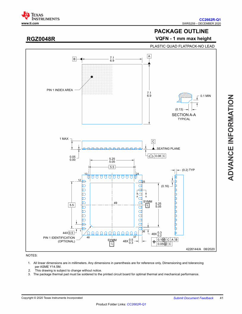
www.ti.comCC2662R-Q1
SWRS259 – DECEMBER 2020
AD
VAN
CE
INFO
RM
ATIO
N
Copyright © 2020 Texas Instruments Incorporated Submit Document Feedback 41
Product Folder Links: CC2662R-Q1

CC2662R-Q1SWRS259 – DECEMBER 2020 www.ti.com
AD
VAN
CE IN
FOR
MATIO
N
42 Submit Document Feedback Copyright © 2020 Texas Instruments Incorporated
Product Folder Links: CC2662R-Q1

www.ti.comCC2662R-Q1
SWRS259 – DECEMBER 2020
AD
VAN
CE
INFO
RM
ATIO
N
Copyright © 2020 Texas Instruments Incorporated Submit Document Feedback 43
Product Folder Links: CC2662R-Q1
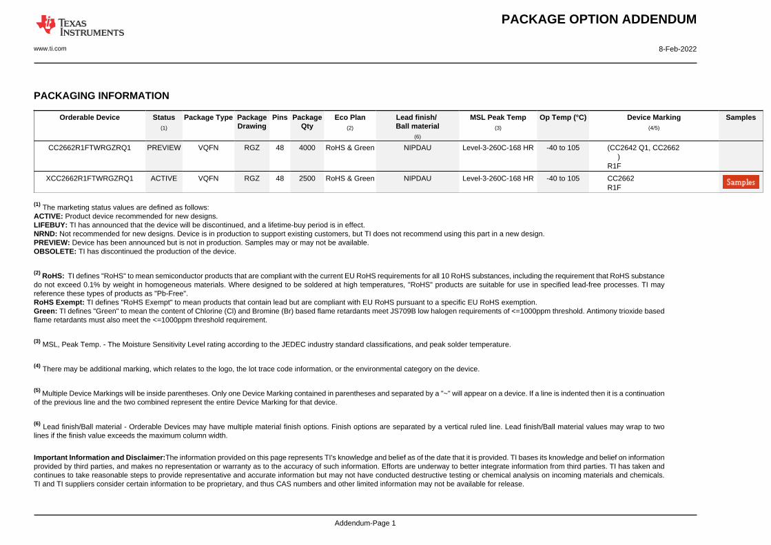
PACKAGE OPTION ADDENDUM
www.ti.com 8-Feb-2022
Addendum-Page 1
PACKAGING INFORMATION
Orderable Device Status(1)
Package Type PackageDrawing
Pins PackageQty
Eco Plan(2)
Lead finish/Ball material
(6)
MSL Peak Temp(3)
Op Temp (°C) Device Marking(4/5)
Samples
CC2662R1FTWRGZRQ1 PREVIEW VQFN RGZ 48 4000 RoHS & Green NIPDAU Level-3-260C-168 HR -40 to 105 (CC2642 Q1, CC2662 )R1F
XCC2662R1FTWRGZRQ1 ACTIVE VQFN RGZ 48 2500 RoHS & Green NIPDAU Level-3-260C-168 HR -40 to 105 CC2662R1F
(1) The marketing status values are defined as follows:ACTIVE: Product device recommended for new designs.LIFEBUY: TI has announced that the device will be discontinued, and a lifetime-buy period is in effect.NRND: Not recommended for new designs. Device is in production to support existing customers, but TI does not recommend using this part in a new design.PREVIEW: Device has been announced but is not in production. Samples may or may not be available.OBSOLETE: TI has discontinued the production of the device.
(2) RoHS: TI defines "RoHS" to mean semiconductor products that are compliant with the current EU RoHS requirements for all 10 RoHS substances, including the requirement that RoHS substancedo not exceed 0.1% by weight in homogeneous materials. Where designed to be soldered at high temperatures, "RoHS" products are suitable for use in specified lead-free processes. TI mayreference these types of products as "Pb-Free".RoHS Exempt: TI defines "RoHS Exempt" to mean products that contain lead but are compliant with EU RoHS pursuant to a specific EU RoHS exemption.Green: TI defines "Green" to mean the content of Chlorine (Cl) and Bromine (Br) based flame retardants meet JS709B low halogen requirements of <=1000ppm threshold. Antimony trioxide basedflame retardants must also meet the <=1000ppm threshold requirement.
(3) MSL, Peak Temp. - The Moisture Sensitivity Level rating according to the JEDEC industry standard classifications, and peak solder temperature.
(4) There may be additional marking, which relates to the logo, the lot trace code information, or the environmental category on the device.
(5) Multiple Device Markings will be inside parentheses. Only one Device Marking contained in parentheses and separated by a "~" will appear on a device. If a line is indented then it is a continuationof the previous line and the two combined represent the entire Device Marking for that device.
(6) Lead finish/Ball material - Orderable Devices may have multiple material finish options. Finish options are separated by a vertical ruled line. Lead finish/Ball material values may wrap to twolines if the finish value exceeds the maximum column width.
Important Information and Disclaimer:The information provided on this page represents TI's knowledge and belief as of the date that it is provided. TI bases its knowledge and belief on informationprovided by third parties, and makes no representation or warranty as to the accuracy of such information. Efforts are underway to better integrate information from third parties. TI has taken andcontinues to take reasonable steps to provide representative and accurate information but may not have conducted destructive testing or chemical analysis on incoming materials and chemicals.TI and TI suppliers consider certain information to be proprietary, and thus CAS numbers and other limited information may not be available for release.

PACKAGE OPTION ADDENDUM
www.ti.com 8-Feb-2022
Addendum-Page 2
In no event shall TI's liability arising out of such information exceed the total purchase price of the TI part(s) at issue in this document sold by TI to Customer on an annual basis.

www.ti.com
GENERIC PACKAGE VIEW
Images above are just a representation of the package family, actual package may vary.Refer to the product data sheet for package details.
VQFN - 1 mm max heightRGZ 48PLASTIC QUADFLAT PACK- NO LEAD7 x 7, 0.5 mm pitch
4224671/A

IMPORTANT NOTICE AND DISCLAIMERTI PROVIDES TECHNICAL AND RELIABILITY DATA (INCLUDING DATA SHEETS), DESIGN RESOURCES (INCLUDING REFERENCE DESIGNS), APPLICATION OR OTHER DESIGN ADVICE, WEB TOOLS, SAFETY INFORMATION, AND OTHER RESOURCES “AS IS” AND WITH ALL FAULTS, AND DISCLAIMS ALL WARRANTIES, EXPRESS AND IMPLIED, INCLUDING WITHOUT LIMITATION ANY IMPLIED WARRANTIES OF MERCHANTABILITY, FITNESS FOR A PARTICULAR PURPOSE OR NON-INFRINGEMENT OF THIRD PARTY INTELLECTUAL PROPERTY RIGHTS.These resources are intended for skilled developers designing with TI products. You are solely responsible for (1) selecting the appropriate TI products for your application, (2) designing, validating and testing your application, and (3) ensuring your application meets applicable standards, and any other safety, security, regulatory or other requirements.These resources are subject to change without notice. TI grants you permission to use these resources only for development of an application that uses the TI products described in the resource. Other reproduction and display of these resources is prohibited. No license is granted to any other TI intellectual property right or to any third party intellectual property right. TI disclaims responsibility for, and you will fully indemnify TI and its representatives against, any claims, damages, costs, losses, and liabilities arising out of your use of these resources.TI’s products are provided subject to TI’s Terms of Sale or other applicable terms available either on ti.com or provided in conjunction with such TI products. TI’s provision of these resources does not expand or otherwise alter TI’s applicable warranties or warranty disclaimers for TI products.TI objects to and rejects any additional or different terms you may have proposed. IMPORTANT NOTICE
Mailing Address: Texas Instruments, Post Office Box 655303, Dallas, Texas 75265Copyright © 2022, Texas Instruments Incorporated


![CC3200 SimpleLink Wi-Fi and IoT Solution with MCU ... · CC3200 SimpleLink™ Wi-Fi® and IoT Solution with MCU LaunchPad Hardware ... 3.1 Development Environment ... 0] 100 = Flash](https://static.fdocuments.us/doc/165x107/5b735eac7f8b9a58028e618c/cc3200-simplelink-wi-fi-and-iot-solution-with-mcu-cc3200-simplelink-wi-fi.jpg)