CC 8-bit Microcontroller with 16K/ 32K byte Flash ... Sheets/Atmel PDFs...7 T89C51RB2/RC2...
116
Rev. 4105C–8051–02/02 1 Features • 80C52 Compatible – 8051 Pin and Instruction Compatible – Four 8-bit I/O Ports – Three 16-bit timer/counters – 256 Bytes Scratch Pad RAM – 10 Interrupt Sources with 4 Priority Levels – Dual Data Pointer • Variable Length MOVX for slow RAM/Peripherals • ISP (In-System Programming) using Standard V CC Power Supply • Boot ROM Contains Low Level FLASH Programming Routines and a Default Serial Loader • High-Speed Architecture – 40 MHz in Standard Mode – 20 MHz in X2 Mode (6 clocks/machine cycle) • 16K/32K Bytes on-chip FLASH Program/Data Memory – Byte and Page (128 Bytes) Erase and Write – 10k Write Cycles • On-chip 1024 Bytes Expanded RAM (XRAM) – Software Selectable Size (0, 256, 512, 768, 1024 bytes) – 256 Bytes Selected at Reset for TS87C51RB2/RC2 Compatibility • Keyboard Interrupt Interface on port P1 • SPI Interface (Master / Slave Mode) • 8-bit Clock Prescaler • Improved X2 Mode with Independent Selection for CPU and each Peripheral • Programmable Counter Array 5 Channels with: – High Speed Output – Compare / Capture – Pulse Width Modulator – Watchdog Timer Capabilities • Asynchronous Port Reset • Full Duplex Enhanced UART • Dedicated Baud Rate Generator for UART • Low EMI (Inhibit ALE) • Hardware Watchdog Timer (One-time enabled with Reset-Out) • Power Control Modes: – Idle Mode – Power-down mode – Power-off Flag • Power supply: 4.5 to 5.5V or 2.7 to 3.6V • Temperature ranges: Commercial (0 to +70°C) and Industrial (-40°C to +85°C) • Packages: PDIL40, PLCC44, VQFP44 Description T89C51RB2/RC2 is a high-performance FLASH version of the 80C51 8-bit microcon- trollers. It contains a 16K or 32K byte Flash memory block for program and data. The Flash memory can be programmed either in parallel mode or in serial mode with the ISP capability or with software. The programming voltage is internally generated from the standard V CC pin. The T89C51RB2/RC2 retains all features of the 80C52 with 256 bytes of internal RAM, a 7-source 4-level interrupt controller and three timer/counters. In addition, the T89C51RB2/RC2 has a Programmable Counter Array, an XRAM of 1024 bytes, a Hardware Watchdog Timer, a Keyboard Interface, an SPI Interface, 8-bit Microcontroller with 16K/ 32K byte Flash T89C51RB2 T89C51RC2 Preliminary
Transcript of CC 8-bit Microcontroller with 16K/ 32K byte Flash ... Sheets/Atmel PDFs...7 T89C51RB2/RC2...
Rev. 4105C–8051–02/02
1
Features• 80C52 Compatible
– 8051 Pin and Instruction Compatible– Four 8-bit I/O Ports– Three 16-bit timer/counters– 256 Bytes Scratch Pad RAM– 10 Interrupt Sources with 4 Priority Levels– Dual Data Pointer
• Variable Length MOVX for slow RAM/Peripherals• ISP (In-System Programming) using Standard VCC Power Supply• Boot ROM Contains Low Level FLASH Programming Routines and a Default Serial
Loader• High-Speed Architecture
– 40 MHz in Standard Mode– 20 MHz in X2 Mode (6 clocks/machine cycle)
• 16K/32K Bytes on-chip FLASH Program/Data Memory– Byte and Page (128 Bytes) Erase and Write– 10k Write Cycles
• On-chip 1024 Bytes Expanded RAM (XRAM)– Software Selectable Size (0, 256, 512, 768, 1024 bytes)– 256 Bytes Selected at Reset for TS87C51RB2/RC2 Compatibility
• Keyboard Interrupt Interface on port P1• SPI Interface (Master / Slave Mode)• 8-bit Clock Prescaler• Improved X2 Mode with Independent Selection for CPU and each Peripheral• Programmable Counter Array 5 Channels with:
– High Speed Output– Compare / Capture– Pulse Width Modulator– Watchdog Timer Capabilities
• Asynchronous Port Reset• Full Duplex Enhanced UART• Dedicated Baud Rate Generator for UART• Low EMI (Inhibit ALE)• Hardware Watchdog Timer (One-time enabled with Reset-Out)• Power Control Modes:
– Idle Mode– Power-down mode– Power-off Flag
• Power supply: 4.5 to 5.5V or 2.7 to 3.6V• Temperature ranges: Commercial (0 to +70°C) and Industrial (-40°C to +85°C)• Packages: PDIL40, PLCC44, VQFP44
DescriptionT89C51RB2/RC2 is a high-performance FLASH version of the 80C51 8-bit microcon-trollers. It contains a 16K or 32K byte Flash memory block for program and data.
The Flash memory can be programmed either in parallel mode or in serial mode withthe ISP capability or with software. The programming voltage is internally generatedfrom the standard VCC pin.
The T89C51RB2/RC2 retains all features of the 80C52 with 256 bytes of internalRAM, a 7-source 4-level interrupt controller and three timer/counters.
In addition, the T89C51RB2/RC2 has a Programmable Counter Array, an XRAM of1024 bytes, a Hardware Watchdog Timer, a Keyboard Interface, an SPI Interface,
8-bitMicrocontrollerwith 16K/32K byte Flash
T89C51RB2T89C51RC2
Preliminary
2 T89C51RB2/RC24105C–8051–02/02
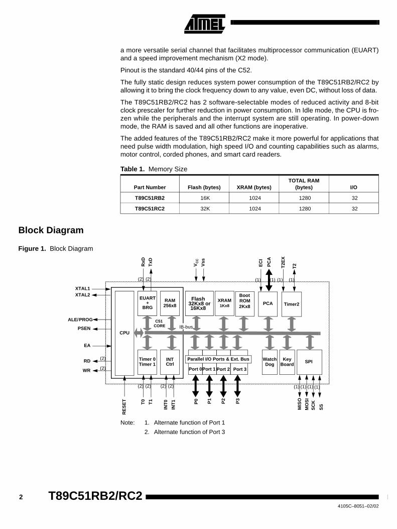
a more versatile serial channel that facilitates multiprocessor communication (EUART)and a speed improvement mechanism (X2 mode).
Pinout is the standard 40/44 pins of the C52.
The fully static design reduces system power consumption of the T89C51RB2/RC2 byallowing it to bring the clock frequency down to any value, even DC, without loss of data.
The T89C51RB2/RC2 has 2 software-selectable modes of reduced activity and 8-bitclock prescaler for further reduction in power consumption. In Idle mode, the CPU is fro-zen while the peripherals and the interrupt system are still operating. In power-downmode, the RAM is saved and all other functions are inoperative.
The added features of the T89C51RB2/RC2 make it more powerful for applications thatneed pulse width modulation, high speed I/O and counting capabilities such as alarms,motor control, corded phones, and smart card readers.
Block Diagram
Figure 1. Block Diagram
Note: 1. Alternate function of Port 1
2. Alternate function of Port 3
Table 1. Memory Size
Part Number Flash (bytes) XRAM (bytes)TOTAL RAM
(bytes) I/O
T89C51RB2 16K 1024 1280 32
T89C51RC2 32K 1024 1280 32
Timer 0 INT
RAM256x8
T0
T1
RxD
TxD
WR
RD
EA
PSEN
ALE/
XTAL2XTAL1
EUART
CPU
Timer 1
INT
1
Ctrl
INT
0
(2)
(2)
C51CORE
(2) (2) (2) (2)
Port 0
P0
Port 1 Port 2 Port 3
Parallel I/O Ports & Ext. Bus
P1
P2
P3
XRAM1Kx8
IB-bus
PCA
RE
SE
T
PROG
WatchDog
PC
A
EC
I
Vss
VC
C
(2)(2) (1)(1)
Timer2
T2E
X
T2
(1) (1)
Flash32Kx8 or16Kx8
KeyBoard
ROM2Kx8
Boot
+BRG
SPI
MIS
O
MO
SI
SC
K
(1) (1) (1)
SS
(1)
3
T89C51RB2/RC2
4105C–8051–02/02
SFR Mapping The Special Function Registers (SFRs) of the T89C51RB2/RC2 fall into the followingcategories:
• C51 core registers: ACC, B, DPH, DPL, PSW, SP
• I/O port registers: P0, P1, P2, P3
• Timer registers: T2CON, T2MOD, TCON, TH0, TH1, TH2, TMOD, TL0, TL1, TL2,RCAP2L, RCAP2H
• Serial I/O port registers: SADDR, SADEN, SBUF, SCON
• PCA (Programmable Counter Array) registers: CCON, CCAPMx, CL, CH, CCAPxH,CCAPxL (x: 0 to 4)
• Power and clock control registers: PCON
• Hardware Watchdog Timer registers: WDTRST, WDTPRG
• Interrupt system registers: IE0, IPL0, IPH0, IE1, IPL1, IPH1
• Keyboard Interface registers: KBE, KBF, KBLS
• SPI registers: SPCON, SPSTR, SPDAT
• BRG (Baud Rate Generator) registers: BRL, BDRCON
• Flash register: FCON
• Clock Prescaler register: CKRL
• Others: AUXR, AUXR1, CKCON0, CKCON1
4 T89C51RB2/RC24105C–8051–02/02
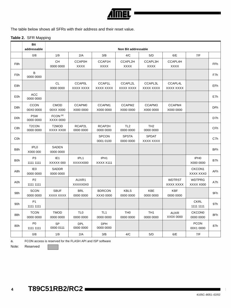
The table below shows all SFRs with their address and their reset value.
Table 2. SFR Mapping
Bit
addressable Non Bit addressable
0/8 1/9 2/A 3/B 4/C 5/D 6/E 7/F
F8hCH
0000 0000
CCAP0H
XXXX
CCAP1H
XXXX
CCAPL2H
XXXX
CCAPL3H
XXXX
CCAPL4H
XXXXFFh
F0hB
0000 0000F7h
E8hCL
0000 0000
CCAP0L
XXXX XXXX
CCAP1L
XXXX XXXX
CCAPL2L
XXXX XXXX
CCAPL3L
XXXX XXXX
CCAPL4L
XXXX XXXXEFh
E0hACC
0000 0000E7h
D8hCCON
00X0 0000
CMOD
00XX X000
CCAPM0
X000 0000
CCAPM1
X000 0000
CCAPM2
X000 0000
CCAPM3
X000 0000
CCAPM4
X000 0000DFh
D0hPSW
0000 0000FCON (a)
XXXX 0000
a. FCON access is reserved for the FLASH API and ISP software
Note: Reserved
D7h
C8hT2CON
0000 0000T2MOD
XXXX XX00RCAP2L
0000 0000RCAP2H
0000 0000TL2
0000 0000TH2
0000 0000CFh
C0hSPCON
0001 0100
SPSTA
0000 0000
SPDAT
XXXX XXXXC7h
B8hIPL0
X000 000
SADEN
0000 0000BFh
B0hP3
1111 1111
IE1
XXXXX 000
IPL1
XXXXX000
IPH1
XXXX X111
IPH0
X000 0000B7h
A8hIE0
0000 0000
SADDR
0000 0000
CKCON1
XXXX XXX0AFh
A0hP2
1111 1111
AUXR1
XXXXX0X0
WDTRST
XXXX XXXX
WDTPRG
XXXX X000A7h
98hSCON
0000 0000
SBUF
XXXX XXXX
BRL
0000 0000
BDRCON
XXX0 0000
KBLS
0000 0000
KBE
0000 0000
KBF
0000 00009Fh
90hP1
1111 1111
CKRL
1111 111197h
88hTCON
0000 0000
TMOD
0000 0000
TL0
0000 0000
TL1
0000 0000
TH0
0000 0000
TH1
0000 0000AUXR
XX0X 0000CKCON0
0000 00008Fh
80hP0
1111 1111SP
0000 0111DPL
0000 0000DPH
0000 0000PCON
00X1 000087h
0/8 1/9 2/A 3/B 4/C 5/D 6/E 7/F
5
T89C51RB2/RC2
4105C–8051–02/02
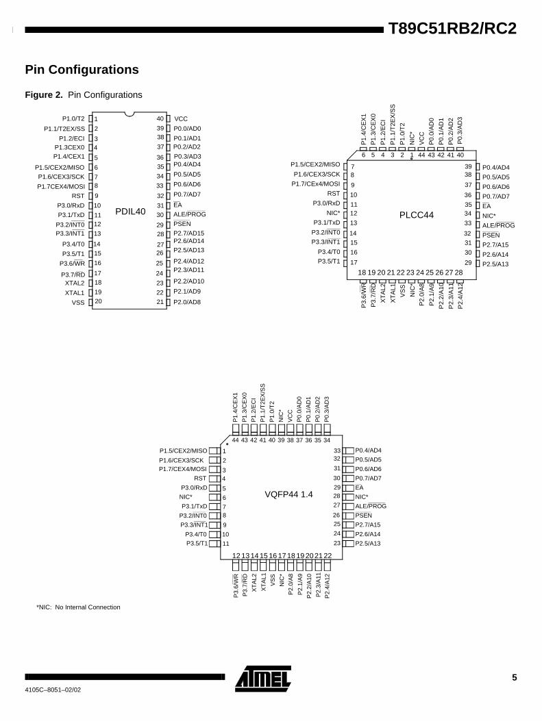
Pin Configurations
Figure 2. Pin Configurations
P1.7CEX4/MOSI
P1.4/CEX1
RST
P3.0/RxD
P3.1/TxD
P1.3CEX0
1
P1.5/CEX2/MISO
P1.6/CEX3/SCK
P3.2/INT0P3.3/INT1
P3.4/T0
P3.5/T1
P3.6/WR
P3.7/RDXTAL2
XTAL1
VSS P2.0/AD8
P2.1/AD9
P2.2/AD10
P2.3/AD11P2.4/AD12
P0.4/AD4
P0.6/AD6
P0.5/AD5
P0.7/AD7
ALE/PROG
PSEN
EA
P2.7/AD15
P2.5/AD13
P2.6/AD14
P1.0/T2
P1.2/ECI
P1.1/T2EX/SS
VCC
P0.0/AD0
P0.1/AD1P0.2/AD2
P0.3/AD3
PDIL40
2
34
5
6
78
9
10
1112
13
14
15
16
17
18
19
20
40
3938
37
36
35
34
33
32
31
30
2928
2726
25
24
23
22
21
43 42 41 40 3944 38 37 36 35 34
P1.
4/C
EX
1
P1.
0/T
2
P1.
1/T
2EX
/SS
P1.
3/C
EX
0
P1.
2/E
CI
NIC
*
VC
C
P0.
0/A
D0
P0.
2/A
D2
P0.
3/A
D3
P0.
1/A
D1
P0.4/AD4
P0.6/AD6
P0.5/AD5
P0.7/AD7
ALE/PROG
PSEN
EA
NIC*
P2.7/A15
P2.5/A13
P2.6/A14
P1.5/CEX2/MISO
P1.6/CEX3/SCKP1.7/CEX4/MOSI
RST
P3.0/RxD
NIC*
P3.1/TxD
P3.2/INT0
P3.3/INT1
P3.4/T0
P3.5/T1
P3.
6/W
R
P3.
7/R
D
XT
AL2
XT
AL1
VS
S
P2.
0/A
8
P2.
1/A
9
P2.
2/A
10
P2.
3/A
11
P2.
4/A
12
NIC
*
12 13 17161514 201918 21 22
3332
31
30
2928
27
26
25
24
23
VQFP44 1.4
1
2
34
5
6
78
9
10
11
18 19 23222120 262524 27 28
5 4 3 2 16 44 43 42 41 40
P1.
4/C
EX
1
P1.
0/T
2
P1.
1/T
2EX
/SS
P1.
3/C
EX
0
P1.
2/E
CI
NIC
*
VC
C
P0.
0/A
D0
P0.
2/A
D2
P0.
1/A
D1
P0.4/AD4
P0.6/AD6
P0.5/AD5
P0.7/AD7
ALE/PROG
PSEN
EA
NIC*
P2.7/A15
P2.5/A13
P2.6/A14
P3.
6/W
R
P3.
7/R
D
XT
AL2
XT
AL1
VS
S
P2.
0/A
8
P2.
1/A
9
P2.
2/A
10
P2.
3/A
11
P2.
4/A
12
P1.5/CEX2/MISO
P1.6/CEX3/SCK
P1.7/CEx4/MOSI
RST
P3.0/RxD
NIC*
P3.1/TxD
P3.2/INT0
P3.3/INT1
P3.4/T0
P3.5/T1
P0.
3/A
D3
NIC
*
78
9
10
1112
13
14
15
16
17
3938
37
36
3534
33
32
31
30
29
PLCC44
*NIC: No Internal Connection
6 T89C51RB2/RC24105C–8051–02/02
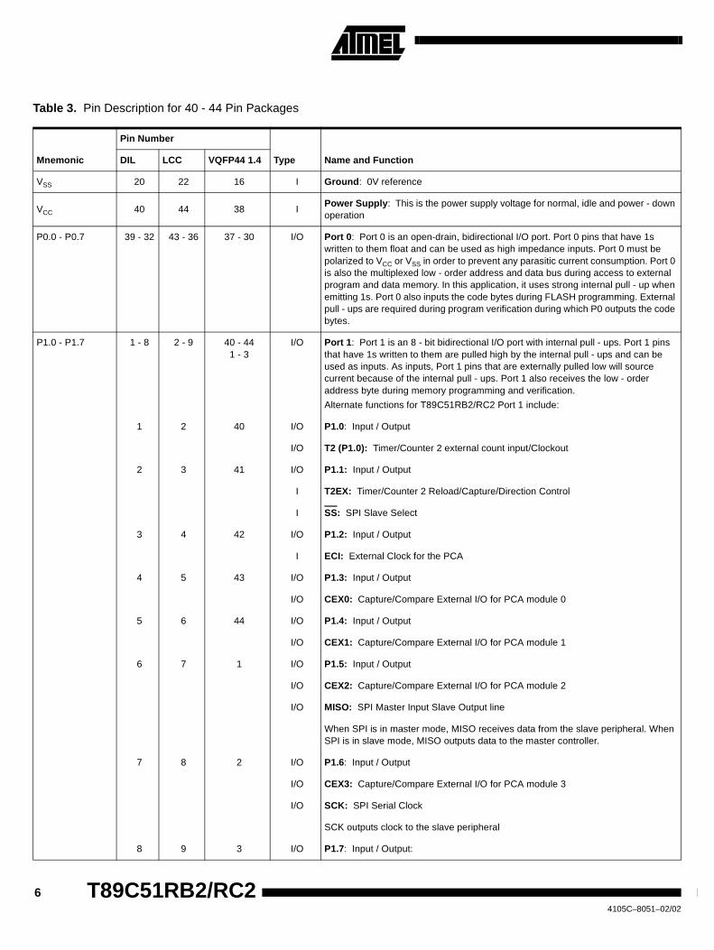
Table 3. Pin Description for 40 - 44 Pin Packages
Mnemonic
Pin Number
Type Name and FunctionDIL LCC VQFP44 1.4
VSS 20 22 16 I Ground: 0V reference
VCC 40 44 38 IPower Supply: This is the power supply voltage for normal, idle and power - downoperation
P0.0 - P0.7 39 - 32 43 - 36 37 - 30 I/O Port 0: Port 0 is an open-drain, bidirectional I/O port. Port 0 pins that have 1swritten to them float and can be used as high impedance inputs. Port 0 must bepolarized to VCC or VSS in order to prevent any parasitic current consumption. Port 0is also the multiplexed low - order address and data bus during access to externalprogram and data memory. In this application, it uses strong internal pull - up whenemitting 1s. Port 0 also inputs the code bytes during FLASH programming. Externalpull - ups are required during program verification during which P0 outputs the codebytes.
P1.0 - P1.7 1 - 8 2 - 9 40 - 441 - 3
I/O Port 1: Port 1 is an 8 - bit bidirectional I/O port with internal pull - ups. Port 1 pinsthat have 1s written to them are pulled high by the internal pull - ups and can beused as inputs. As inputs, Port 1 pins that are externally pulled low will sourcecurrent because of the internal pull - ups. Port 1 also receives the low - orderaddress byte during memory programming and verification.
Alternate functions for T89C51RB2/RC2 Port 1 include:
1 2 40 I/O P1.0: Input / Output
I/O T2 (P1.0): Timer/Counter 2 external count input/Clockout
2 3 41 I/O P1.1: Input / Output
I T2EX: Timer/Counter 2 Reload/Capture/Direction Control
I SS: SPI Slave Select
3 4 42 I/O P1.2: Input / Output
I ECI: External Clock for the PCA
4 5 43 I/O P1.3: Input / Output
I/O CEX0: Capture/Compare External I/O for PCA module 0
5 6 44 I/O P1.4: Input / Output
I/O CEX1: Capture/Compare External I/O for PCA module 1
6 7 1 I/O P1.5: Input / Output
I/O CEX2: Capture/Compare External I/O for PCA module 2
I/O MISO: SPI Master Input Slave Output line
When SPI is in master mode, MISO receives data from the slave peripheral. WhenSPI is in slave mode, MISO outputs data to the master controller.
7 8 2 I/O P1.6: Input / Output
I/O CEX3: Capture/Compare External I/O for PCA module 3
I/O SCK: SPI Serial Clock
SCK outputs clock to the slave peripheral
8 9 3 I/O P1.7: Input / Output:
7
T89C51RB2/RC2
4105C–8051–02/02
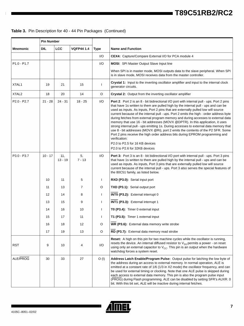
I/O CEX4: Capture/Compare External I/O for PCA module 4
P1.0 - P1.7 I/O MOSI: SPI Master Output Slave Input line
When SPI is in master mode, MOSI outputs data to the slave peripheral. When SPIis in slave mode, MOSI receives data from the master controller.
XTAL1 19 21 15 ICrystal 1: Input to the inverting oscillator amplifier and input to the internal clockgenerator circuits.
XTAL2 18 20 14 O Crystal 2: Output from the inverting oscillator amplifier
P2.0 - P2.7 21 - 28 24 - 31 18 - 25 I/O Port 2: Port 2 is an 8 - bit bidirectional I/O port with internal pull - ups. Port 2 pinsthat have 1s written to them are pulled high by the internal pull - ups and can beused as inputs. As inputs, Port 2 pins that are externally pulled low will sourcecurrent because of the internal pull - ups. Port 2 emits the high - order address byteduring fetches from external program memory and during accesses to external datamemory that use 16 - bit addresses (MOVX @DPTR). In this application, it usesstrong internal pull - ups emitting 1s. During accesses to external data memory thatuse 8 - bit addresses (MOVX @Ri), port 2 emits the contents of the P2 SFR. SomePort 2 pins receive the high order address bits during EPROM programming andverification:
P2.0 to P2.5 for 16 KB devices
P2.0 to P2.6 for 32KB devices
P3.0 - P3.7 10 - 17 11,13 - 19
5,7 - 13
I/O Port 3: Port 3 is an 8 - bit bidirectional I/O port with internal pull - ups. Port 3 pinsthat have 1s written to them are pulled high by the internal pull - ups and can beused as inputs. As inputs, Port 3 pins that are externally pulled low will sourcecurrent because of the internal pull - ups. Port 3 also serves the special features ofthe 80C51 family, as listed below.
10 11 5 I RXD (P3.0): Serial input port
11 13 7 O TXD (P3.1): Serial output port
12 14 8 I INT0 (P3.2): External interrupt 0
13 15 9 I INT1 (P3.3): External interrupt 1
14 16 10 I T0 (P3.4): Timer 0 external input
15 17 11 I T1 (P3.5): Timer 1 external input
16 18 12 O WR (P3.6): External data memory write strobe
17 19 13 O RD (P3.7): External data memory read strobe
RST 9 10 4 I/O
Reset: A high on this pin for two machine cycles while the oscillator is running,resets the device. An internal diffused resistor to VSS permits a power - on resetusing only an external capacitor to VCC. This pin is an output when the hardwarewatchdog forces a system reset.
ALE/PROG 30 33 27 O (I) Address Latch Enable/Program Pulse: Output pulse for latching the low byte ofthe address during an access to external memory. In normal operation, ALE isemitted at a constant rate of 1/6 (1/3 in X2 mode) the oscillator frequency, and canbe used for external timing or clocking. Note that one ALE pulse is skipped duringeach access to external data memory. This pin is also the program pulse input(PROG) during Flash programming. ALE can be disabled by setting SFR’s AUXR. 0bit. With this bit set, ALE will be inactive during internal fetches.
Table 3. Pin Description for 40 - 44 Pin Packages (Continued)
Mnemonic
Pin Number
Type Name and FunctionDIL LCC VQFP44 1.4
8 T89C51RB2/RC24105C–8051–02/02
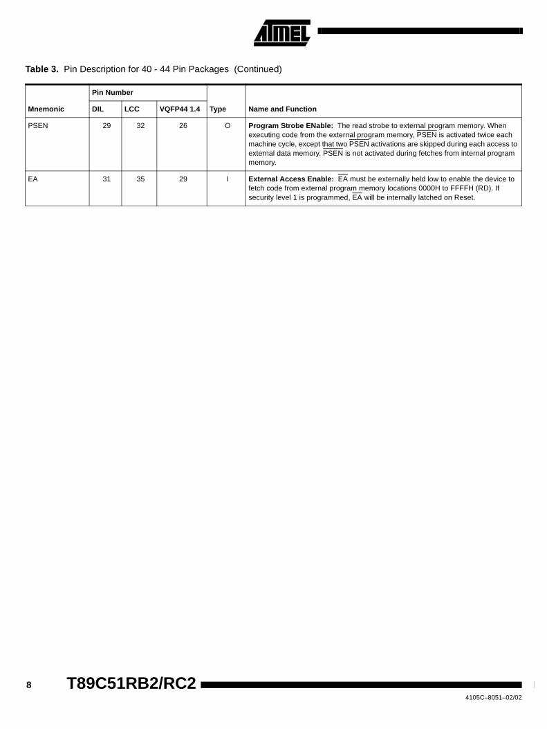
PSEN 29 32 26 O Program Strobe ENable: The read strobe to external program memory. Whenexecuting code from the external program memory, PSEN is activated twice eachmachine cycle, except that two PSEN activations are skipped during each access toexternal data memory. PSEN is not activated during fetches from internal programmemory.
EA 31 35 29 I External Access Enable: EA must be externally held low to enable the device tofetch code from external program memory locations 0000H to FFFFH (RD). Ifsecurity level 1 is programmed, EA will be internally latched on Reset.
Table 3. Pin Description for 40 - 44 Pin Packages (Continued)
Mnemonic
Pin Number
Type Name and FunctionDIL LCC VQFP44 1.4
9
T89C51RB2/RC2
4105C–8051–02/02
Oscillator In order to optimize the power consumption and execution time needed for a specifictask, an internal, prescaler feature has been implemented between oscillator and theCPU and peripherals.
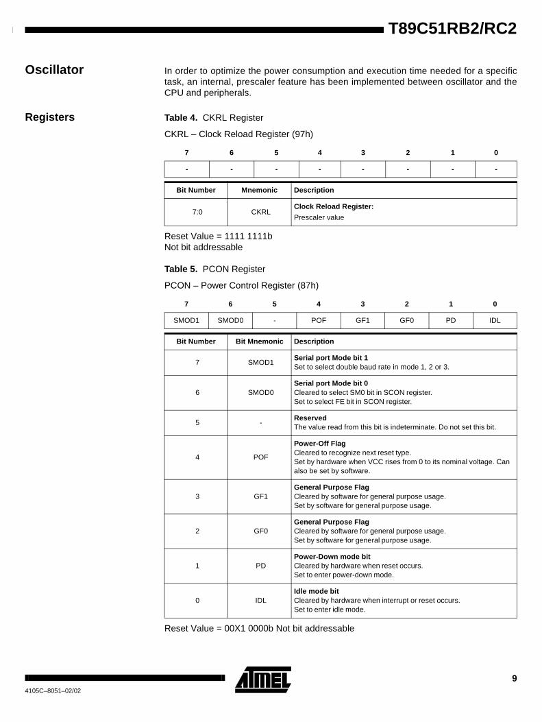
Registers Table 4. CKRL Register
CKRL – Clock Reload Register (97h)
Reset Value = 1111 1111bNot bit addressable
Table 5. PCON Register
PCON – Power Control Register (87h)
Reset Value = 00X1 0000b Not bit addressable
7 6 5 4 3 2 1 0
- - - - - - - -
Bit Number Mnemonic Description
7:0 CKRLClock Reload Register:
Prescaler value
7 6 5 4 3 2 1 0
SMOD1 SMOD0 - POF GF1 GF0 PD IDL
Bit Number Bit Mnemonic Description
7 SMOD1Serial port Mode bit 1Set to select double baud rate in mode 1, 2 or 3.
6 SMOD0Serial port Mode bit 0Cleared to select SM0 bit in SCON register.Set to select FE bit in SCON register.
5 -ReservedThe value read from this bit is indeterminate. Do not set this bit.
4 POF
Power-Off FlagCleared to recognize next reset type.Set by hardware when VCC rises from 0 to its nominal voltage. Canalso be set by software.
3 GF1General Purpose FlagCleared by software for general purpose usage.Set by software for general purpose usage.
2 GF0General Purpose FlagCleared by software for general purpose usage.Set by software for general purpose usage.
1 PDPower-Down mode bitCleared by hardware when reset occurs.Set to enter power-down mode.
0 IDLIdle mode bitCleared by hardware when interrupt or reset occurs.Set to enter idle mode.
10 T89C51RB2/RC24105C–8051–02/02
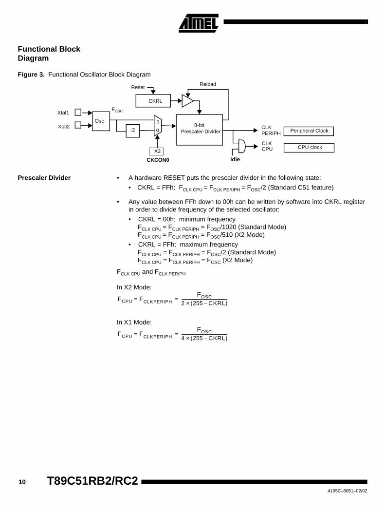
Functional BlockDiagram
Figure 3. Functional Oscillator Block Diagram
Prescaler Divider • A hardware RESET puts the prescaler divider in the following state:
• CKRL = FFh: FCLK CPU = FCLK PERIPH = FOSC/2 (Standard C51 feature)
• Any value between FFh down to 00h can be written by software into CKRL registerin order to divide frequency of the selected oscillator:
• CKRL = 00h: minimum frequencyFCLK CPU = FCLK PERIPH = FOSC/1020 (Standard Mode)FCLK CPU = FCLK PERIPH = FOSC/510 (X2 Mode)
• CKRL = FFh: maximum frequencyFCLK CPU = FCLK PERIPH = FOSC/2 (Standard Mode)FCLK CPU = FCLK PERIPH = FOSC (X2 Mode)
FCLK CPU and FCLK PERIPH
In X2 Mode:
In X1 Mode:
Xtal2
Xtal1
Osc
CLK
Idle
CPU clock
CKRL
Reload
8-bitPrescaler-Divider
Reset
Peripheral Clock:2
X2
0
1
FOSC
CKCON0
CLKPERIPH
CPU
FCPU F= CLKPERIPH
FOSC
2 255 CKRL–( )×-----------------------------------------------=
FCPU F= CLKPERIPH
FOSC
4 255 CKRL–( )×-----------------------------------------------=
11
T89C51RB2/RC2
4105C–8051–02/02
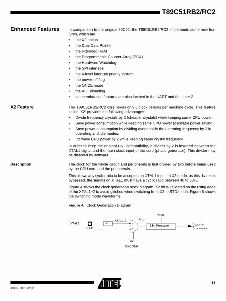
Enhanced Features In comparison to the original 80C52, the T89C51RB2/RC2 implements some new fea-tures, which are:
• the X2 option
• the Dual Data Pointer
• the extended RAM
• the Programmable Counter Array (PCA)
• the Hardware Watchdog
• the SPI interface
• the 4-level interrupt priority system
• the power-off flag
• the ONCE mode
• the ALE disabling
• some enhanced features are also located in the UART and the timer 2
X2 Feature The T89C51RB2/RC2 core needs only 6 clock periods per machine cycle. This featurecalled ‘X2’ provides the following advantages:
• Divide frequency crystals by 2 (cheaper crystals) while keeping same CPU power.
• Save power consumption while keeping same CPU power (oscillator power saving).
• Save power consumption by dividing dynamically the operating frequency by 2 inoperating and idle modes.
• Increase CPU power by 2 while keeping same crystal frequency.
In order to keep the original C51 compatibility, a divider by 2 is inserted between theXTAL1 signal and the main clock input of the core (phase generator). This divider maybe disabled by software.
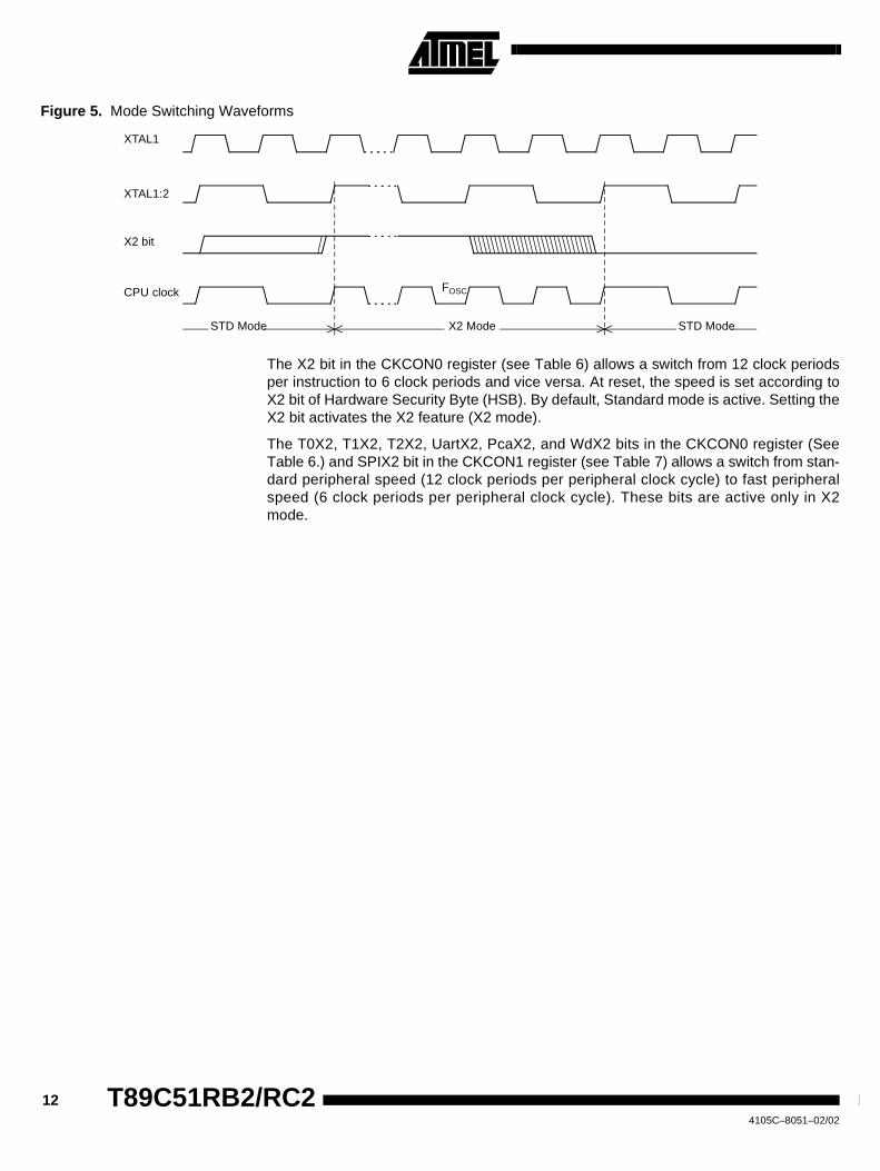
Description The clock for the whole circuit and peripherals is first divided by two before being usedby the CPU core and the peripherals.
This allows any cyclic ratio to be accepted on XTAL1 input. In X2 mode, as this divider isbypassed, the signals on XTAL1 must have a cyclic ratio between 40 to 60%.
Figure 4 shows the clock generation block diagram. X2 bit is validated on the rising edgeof the XTAL1÷2 to avoid glitches when switching from X2 to STD mode. Figure 5 showsthe switching mode waveforms.
Figure 4. Clock Generation Diagram
XTAL1 2
CKCON0
X2
8 bit Prescaler
FOSC
FXTAL0
1
XTAL1:2FCLK CPU
FCLK PERIPH
CKRL
12 T89C51RB2/RC24105C–8051–02/02
Figure 5. Mode Switching Waveforms
The X2 bit in the CKCON0 register (see Table 6) allows a switch from 12 clock periodsper instruction to 6 clock periods and vice versa. At reset, the speed is set according toX2 bit of Hardware Security Byte (HSB). By default, Standard mode is active. Setting theX2 bit activates the X2 feature (X2 mode).
The T0X2, T1X2, T2X2, UartX2, PcaX2, and WdX2 bits in the CKCON0 register (SeeTable 6.) and SPIX2 bit in the CKCON1 register (see Table 7) allows a switch from stan-dard peripheral speed (12 clock periods per peripheral clock cycle) to fast peripheralspeed (6 clock periods per peripheral clock cycle). These bits are active only in X2mode.
XTAL1:2
XTAL1
CPU clock
X2 bit
X2 ModeSTD Mode STD Mode
FOSC
13
T89C51RB2/RC2
4105C–8051–02/02
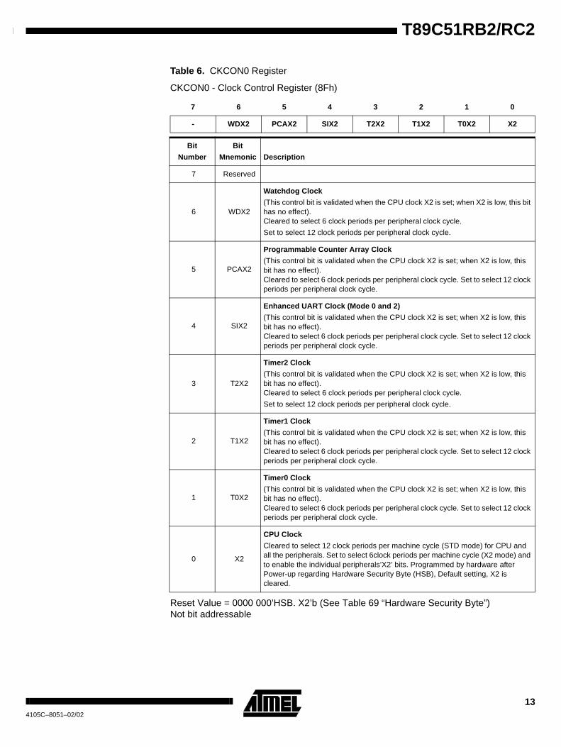
Table 6. CKCON0 Register
CKCON0 - Clock Control Register (8Fh)
Reset Value = 0000 000’HSB. X2’b (See Table 69 “Hardware Security Byte”)Not bit addressable
7 6 5 4 3 2 1 0
- WDX2 PCAX2 SIX2 T2X2 T1X2 T0X2 X2
Bit
Number
Bit
Mnemonic Description
7 Reserved
6 WDX2
Watchdog Clock
(This control bit is validated when the CPU clock X2 is set; when X2 is low, this bithas no effect).Cleared to select 6 clock periods per peripheral clock cycle.
Set to select 12 clock periods per peripheral clock cycle.
5 PCAX2
Programmable Counter Array Clock
(This control bit is validated when the CPU clock X2 is set; when X2 is low, thisbit has no effect).Cleared to select 6 clock periods per peripheral clock cycle. Set to select 12 clockperiods per peripheral clock cycle.
4 SIX2
Enhanced UART Clock (Mode 0 and 2)
(This control bit is validated when the CPU clock X2 is set; when X2 is low, thisbit has no effect).Cleared to select 6 clock periods per peripheral clock cycle. Set to select 12 clockperiods per peripheral clock cycle.
3 T2X2
Timer2 Clock
(This control bit is validated when the CPU clock X2 is set; when X2 is low, thisbit has no effect).Cleared to select 6 clock periods per peripheral clock cycle.
Set to select 12 clock periods per peripheral clock cycle.
2 T1X2
Timer1 Clock
(This control bit is validated when the CPU clock X2 is set; when X2 is low, thisbit has no effect).Cleared to select 6 clock periods per peripheral clock cycle. Set to select 12 clockperiods per peripheral clock cycle.
1 T0X2
Timer0 Clock
(This control bit is validated when the CPU clock X2 is set; when X2 is low, thisbit has no effect).Cleared to select 6 clock periods per peripheral clock cycle. Set to select 12 clockperiods per peripheral clock cycle.
0 X2
CPU Clock
Cleared to select 12 clock periods per machine cycle (STD mode) for CPU andall the peripherals. Set to select 6clock periods per machine cycle (X2 mode) andto enable the individual peripherals’X2’ bits. Programmed by hardware afterPower-up regarding Hardware Security Byte (HSB), Default setting, X2 iscleared.
14 T89C51RB2/RC24105C–8051–02/02
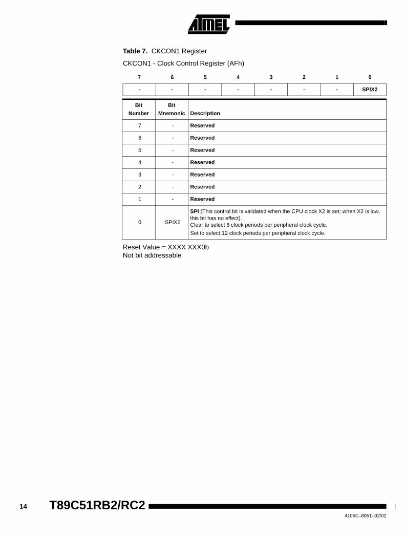
Table 7. CKCON1 Register
CKCON1 - Clock Control Register (AFh)
Reset Value = XXXX XXX0bNot bit addressable
7 6 5 4 3 2 1 0
- - - - - - - SPIX2
Bit
Number
Bit
Mnemonic Description
7 - Reserved
6 - Reserved
5 - Reserved
4 - Reserved
3 - Reserved
2 - Reserved
1 - Reserved
0 SPIX2
SPI (This control bit is validated when the CPU clock X2 is set; when X2 is low,this bit has no effect).Clear to select 6 clock periods per peripheral clock cycle.
Set to select 12 clock periods per peripheral clock cycle.
15
T89C51RB2/RC2
4105C–8051–02/02
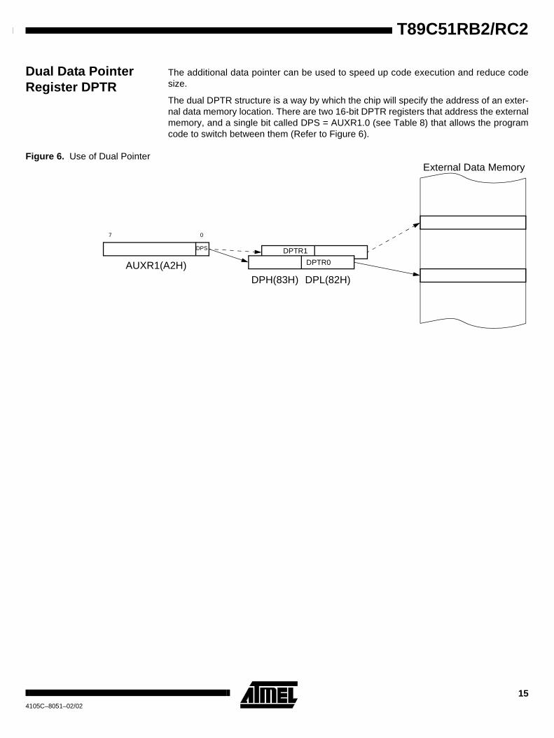
Dual Data PointerRegister DPTR
The additional data pointer can be used to speed up code execution and reduce codesize.
The dual DPTR structure is a way by which the chip will specify the address of an exter-nal data memory location. There are two 16-bit DPTR registers that address the externalmemory, and a single bit called DPS = AUXR1.0 (see Table 8) that allows the programcode to switch between them (Refer to Figure 6).
Figure 6. Use of Dual PointerExternal Data Memory
AUXR1(A2H)
DPS
DPH(83H) DPL(82H)
07
DPTR0
DPTR1
16 T89C51RB2/RC24105C–8051–02/02
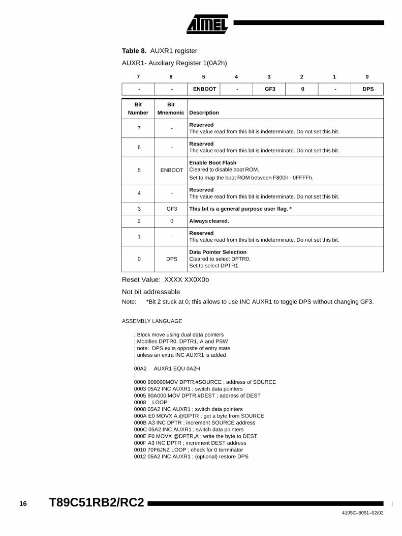
Table 8. AUXR1 register
AUXR1- Auxiliary Register 1(0A2h)
Reset Value: XXXX XX0X0b
Not bit addressableNote: *Bit 2 stuck at 0; this allows to use INC AUXR1 to toggle DPS without changing GF3.
ASSEMBLY LANGUAGE
; Block move using dual data pointers; Modifies DPTR0, DPTR1, A and PSW; note: DPS exits opposite of entry state; unless an extra INC AUXR1 is added;00A2 AUXR1 EQU 0A2H;0000 909000MOV DPTR,#SOURCE ; address of SOURCE0003 05A2 INC AUXR1 ; switch data pointers0005 90A000 MOV DPTR,#DEST ; address of DEST0008 LOOP:0008 05A2 INC AUXR1 ; switch data pointers000A E0 MOVX A,@DPTR ; get a byte from SOURCE000B A3 INC DPTR ; increment SOURCE address000C 05A2 INC AUXR1 ; switch data pointers000E F0 MOVX @DPTR,A ; write the byte to DEST000F A3 INC DPTR ; increment DEST address0010 70F6JNZ LOOP ; check for 0 terminator0012 05A2 INC AUXR1 ; (optional) restore DPS
7 6 5 4 3 2 1 0
- - ENBOOT - GF3 0 - DPS
Bit
Number
Bit
Mnemonic Description
7 -ReservedThe value read from this bit is indeterminate. Do not set this bit.
6 -ReservedThe value read from this bit is indeterminate. Do not set this bit.
5 ENBOOTEnable Boot FlashCleared to disable boot ROM.
Set to map the boot ROM between F800h - 0FFFFh.
4 -ReservedThe value read from this bit is indeterminate. Do not set this bit.
3 GF3 This bit is a general purpose user flag. *
2 0 Always cleared.
1 -ReservedThe value read from this bit is indeterminate. Do not set this bit.
0 DPSData Pointer SelectionCleared to select DPTR0.Set to select DPTR1.
17
T89C51RB2/RC2
4105C–8051–02/02
INC is a short (2 bytes) and fast (12 clocks) way to manipulate the DPS bit in the AUXR1SFR. However, note that the INC instruction does not directly force the DPS bit to a par-ticular state, but simply toggles it. In simple routines, such as the block move example,only the fact that DPS is toggled in the proper sequence matters, not its actual value. Inother words, the block move routine works the same whether DPS is '0' or '1' on entry.Observe that without the last instruction (INC AUXR1), the routine will exit with DPS inthe opposite state.
18 T89C51RB2/RC24105C–8051–02/02
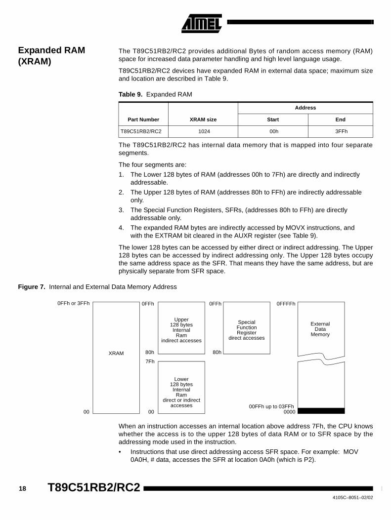
Expanded RAM(XRAM)
The T89C51RB2/RC2 provides additional Bytes of random access memory (RAM)space for increased data parameter handling and high level language usage.
T89C51RB2/RC2 devices have expanded RAM in external data space; maximum sizeand location are described in Table 9.
Table 9. Expanded RAM
The T89C51RB2/RC2 has internal data memory that is mapped into four separatesegments.
The four segments are:
1. The Lower 128 bytes of RAM (addresses 00h to 7Fh) are directly and indirectlyaddressable.
2. The Upper 128 bytes of RAM (addresses 80h to FFh) are indirectly addressableonly.
3. The Special Function Registers, SFRs, (addresses 80h to FFh) are directlyaddressable only.
4. The expanded RAM bytes are indirectly accessed by MOVX instructions, andwith the EXTRAM bit cleared in the AUXR register (see Table 9).
The lower 128 bytes can be accessed by either direct or indirect addressing. The Upper128 bytes can be accessed by indirect addressing only. The Upper 128 bytes occupythe same address space as the SFR. That means they have the same address, but arephysically separate from SFR space.
Figure 7. Internal and External Data Memory Address
When an instruction accesses an internal location above address 7Fh, the CPU knowswhether the access is to the upper 128 bytes of data RAM or to SFR space by theaddressing mode used in the instruction.
• Instructions that use direct addressing access SFR space. For example: MOV0A0H, # data, accesses the SFR at location 0A0h (which is P2).
Part Number XRAM size
Address
Start End
T89C51RB2/RC2 1024 00h 3FFh
XRAM
Upper128 bytesInternal
Ram
Lower128 bytesInternal
Ram
SpecialFunctionRegister
80h 80h
00
0FFh or 3FFh 0FFh
00
0FFh
ExternalData
Memory
000000FFh up to 03FFh
0FFFFh
indirect accesses direct accesses
direct or indirectaccesses
7Fh
19
T89C51RB2/RC2
4105C–8051–02/02
• Instructions that use indirect addressing access the Upper 128 bytes of data RAM.For example: MOV @R0, # data where R0 contains 0A0h, accesses the data byteat address 0A0h, rather than P2 (whose address is 0A0h).
• The XRAM bytes can be accessed by indirect addressing, with EXTRAM bit clearedand MOVX instructions. This part of memory which is physically located on-chip,logically occupies the first bytes of external data memory. The bits XRS0 and XRS1are used to hide a part of the available XRAM as explained in Table 9. This can beuseful if external peripherals are mapped at addresses already used by the internalXRAM.
• With EXTRAM = 0, the XRAM is indirectly addressed, using the MOVX instruction incombination with any of the registers R0, R1 of the selected bank or DPTR. Anaccess to XRAM will not affect ports P0, P2, P3.6 (WR) and P3.7 (RD). Forexample, with EXTRAM = 0, MOVX @R0, # data where R0 contains 0A0H,accesses the XRAM at address 0A0H rather than external memory. An access toexternal data memory locations higher than the accessible size of the XRAM will beperformed with the MOVX DPTR instructions in the same way as in the standard80C51, with P0 and P2 as data/address busses, and P3.6 and P3.7 as write andread timing signals. Accesses to XRAM above 0FFH can only be done by the use ofDPTR.
• With EXTRAM = 1, MOVX @Ri and MOVX @DPTR will be similar to the standard80C51.MOVX @ Ri will provide an eight-bit address multiplexed with data on Port0and any output port pins can be used to output higher order address bits. This is toprovide the external paging capability. MOVX @DPTR will generate a sixteen-bitaddress. Port2 outputs the high-order eight address bits (the contents of DPH) whilePort0 multiplexes the low-order eight address bits (DPL) with data. MOVX @ Ri andMOVX @DPTR will generate either read or write signals on P3.6 (WR) and P3.7(RD).
The stack pointer (SP) may be located anywhere in the 256 bytes RAM (lower andupper RAM) internal data memory. The stack may not be located in the XRAM.
The M0 bit allows to stretch the XRAM timings; if M0 is set, the read and write pulsesare extended from 6 to 30 clock periods. This is useful to access external slowperipherals.
20 T89C51RB2/RC24105C–8051–02/02
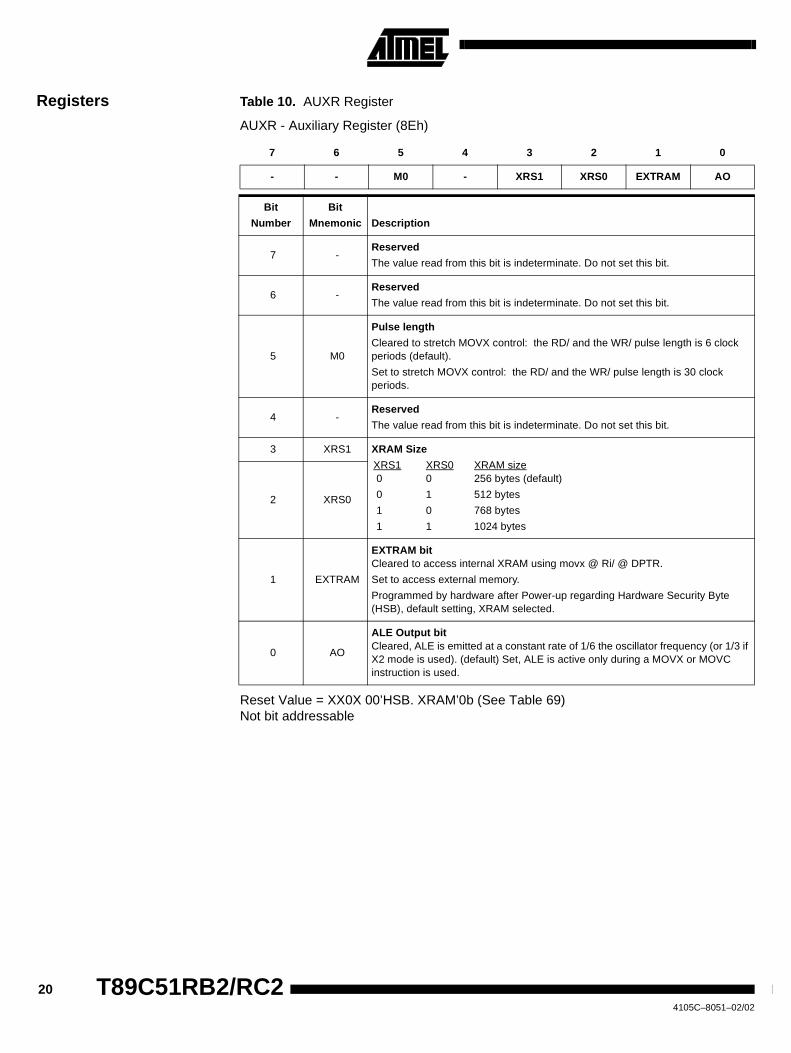
Registers Table 10. AUXR Register
AUXR - Auxiliary Register (8Eh)
Reset Value = XX0X 00’HSB. XRAM’0b (See Table 69)Not bit addressable
7 6 5 4 3 2 1 0
- - M0 - XRS1 XRS0 EXTRAM AO
Bit
Number
Bit
Mnemonic Description
7 -Reserved
The value read from this bit is indeterminate. Do not set this bit.
6 -Reserved
The value read from this bit is indeterminate. Do not set this bit.
5 M0
Pulse length
Cleared to stretch MOVX control: the RD/ and the WR/ pulse length is 6 clockperiods (default).
Set to stretch MOVX control: the RD/ and the WR/ pulse length is 30 clockperiods.
4 -Reserved
The value read from this bit is indeterminate. Do not set this bit.
3 XRS1 XRAM Size
XRS1 XRS0 XRAM size0 0 256 bytes (default)
0 1 512 bytes
1 0 768 bytes
1 1 1024 bytes
2 XRS0
1 EXTRAM
EXTRAM bitCleared to access internal XRAM using movx @ Ri/ @ DPTR.
Set to access external memory.
Programmed by hardware after Power-up regarding Hardware Security Byte(HSB), default setting, XRAM selected.
0 AO
ALE Output bitCleared, ALE is emitted at a constant rate of 1/6 the oscillator frequency (or 1/3 ifX2 mode is used). (default) Set, ALE is active only during a MOVX or MOVCinstruction is used.
21
T89C51RB2/RC2
4105C–8051–02/02
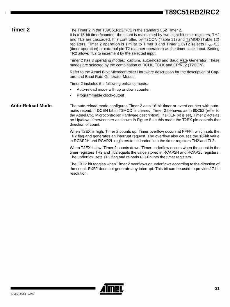
Timer 2 The Timer 2 in the T89C51RB2/RC2 is the standard C52 Timer 2.It is a 16-bit timer/counter: the count is maintained by two eight-bit timer registers, TH2and TL2 are cascaded. It is controlled by T2CON (Table 11) and T2MOD (Table 12)registers. Timer 2 operation is similar to Timer 0 and Timer 1.C/T2 selects FOSC/12(timer operation) or external pin T2 (counter operation) as the timer clock input. SettingTR2 allows TL2 to increment by the selected input.
Timer 2 has 3 operating modes: capture, autoreload and Baud Rate Generator. Thesemodes are selected by the combination of RCLK, TCLK and CP/RL2 (T2CON).
Refer to the Atmel 8-bit Microcontroller Hardware description for the description of Cap-ture and Baud Rate Generator Modes.
Timer 2 includes the following enhancements:
• Auto-reload mode with up or down counter
• Programmable clock-output
Auto-Reload Mode The auto-reload mode configures Timer 2 as a 16-bit timer or event counter with auto-matic reload. If DCEN bit in T2MOD is cleared, Timer 2 behaves as in 80C52 (refer tothe Atmel C51 Microcontroller Hardware description). If DCEN bit is set, Timer 2 acts asan Up/down timer/counter as shown in Figure 8. In this mode the T2EX pin controls thedirection of count.
When T2EX is high, Timer 2 counts up. Timer overflow occurs at FFFFh which sets theTF2 flag and generates an interrupt request. The overflow also causes the 16-bit valuein RCAP2H and RCAP2L registers to be loaded into the timer registers TH2 and TL2.
When T2EX is low, Timer 2 counts down. Timer underflow occurs when the count in thetimer registers TH2 and TL2 equals the value stored in RCAP2H and RCAP2L registers.The underflow sets TF2 flag and reloads FFFFh into the timer registers.
The EXF2 bit toggles when Timer 2 overflows or underflows according to the direction ofthe count. EXF2 does not generate any interrupt. This bit can be used to provide 17-bitresolution.
22 T89C51RB2/RC24105C–8051–02/02
Figure 8. Auto-Reload Mode Up/Down Counter (DCEN = 1)
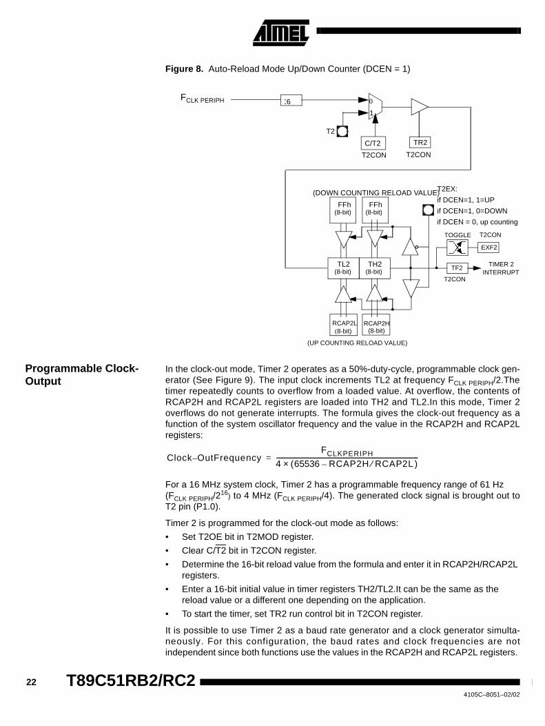
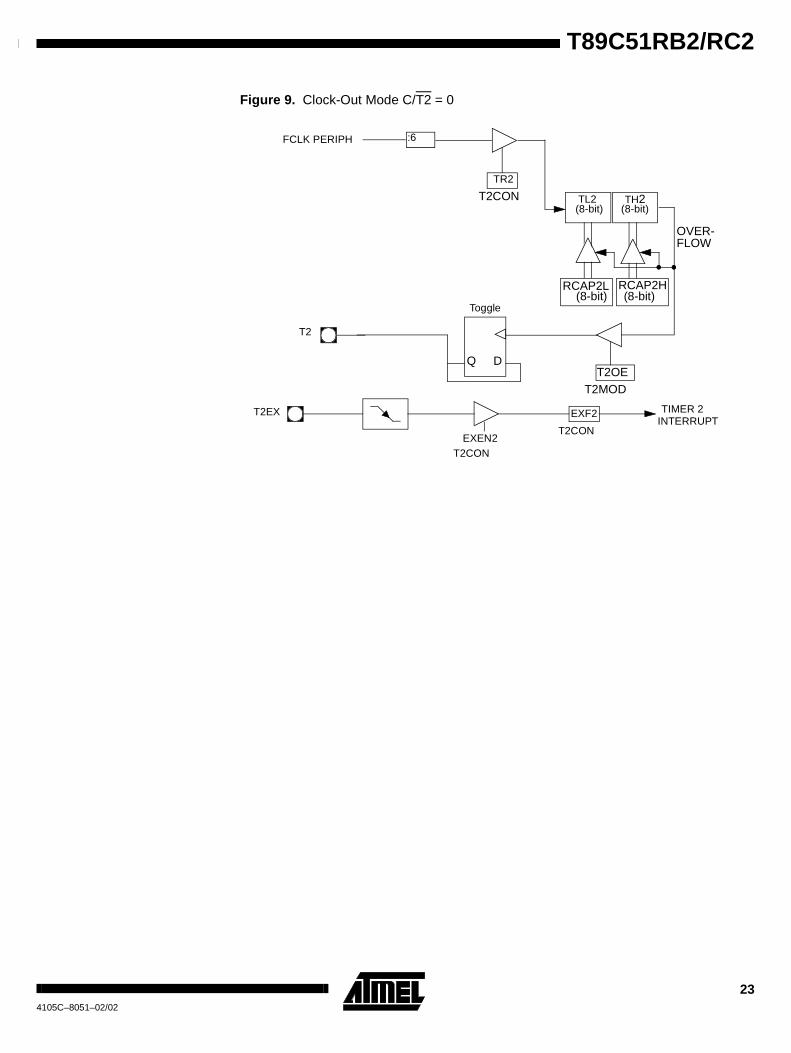
Programmable Clock-Output
In the clock-out mode, Timer 2 operates as a 50%-duty-cycle, programmable clock gen-erator (See Figure 9). The input clock increments TL2 at frequency FCLK PERIPH/2.Thetimer repeatedly counts to overflow from a loaded value. At overflow, the contents ofRCAP2H and RCAP2L registers are loaded into TH2 and TL2.In this mode, Timer 2overflows do not generate interrupts. The formula gives the clock-out frequency as afunction of the system oscillator frequency and the value in the RCAP2H and RCAP2Lregisters:
For a 16 MHz system clock, Timer 2 has a programmable frequency range of 61 Hz(FCLK PERIPH/216) to 4 MHz (FCLK PERIPH/4). The generated clock signal is brought out toT2 pin (P1.0).
Timer 2 is programmed for the clock-out mode as follows:
• Set T2OE bit in T2MOD register.
• Clear C/T2 bit in T2CON register.
• Determine the 16-bit reload value from the formula and enter it in RCAP2H/RCAP2Lregisters.
• Enter a 16-bit initial value in timer registers TH2/TL2.It can be the same as thereload value or a different one depending on the application.
• To start the timer, set TR2 run control bit in T2CON register.
It is possible to use Timer 2 as a baud rate generator and a clock generator simulta-neously. For this configuration, the baud rates and clock frequencies are notindependent since both functions use the values in the RCAP2H and RCAP2L registers.
(DOWN COUNTING RELOAD VALUE)
C/T2
TF2
TR2
T2
EXF2
TH2(8-bit)
TL2(8-bit)
RCAP2H(8-bit)
RCAP2L(8-bit)
FFh(8-bit)
FFh(8-bit)
TOGGLE
(UP COUNTING RELOAD VALUE)
TIMER 2INTERRUPT
FCLK PERIPH 01
T2CON T2CON
T2CON
T2CON
T2EX:
if DCEN=1, 1=UP
if DCEN=1, 0=DOWN
if DCEN = 0, up counting
:6
Clock O– utFrequencyFCLKPERIPH
4 65536 RCAP2H RCAP2L⁄ )–(×---------------------------------------------------------------------------------------------=
23
T89C51RB2/RC2
4105C–8051–02/02
Figure 9. Clock-Out Mode C/T2 = 0
:6
EXF2
TR2
OVER-FLOW
T2EX
TH2(8-bit)
TL2(8-bit)
TIMER 2
RCAP2H(8-bit)
RCAP2L(8-bit)
T2OE
T2
FCLK PERIPH
T2CON
T2CON
T2CON
T2MOD
INTERRUPT
Q D
Toggle
EXEN2
24 T89C51RB2/RC24105C–8051–02/02
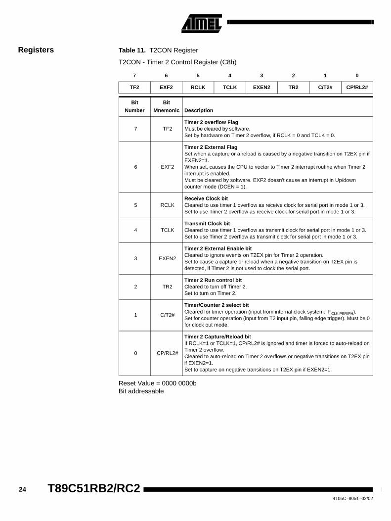
Registers Table 11. T2CON Register
T2CON - Timer 2 Control Register (C8h)
Reset Value = 0000 0000bBit addressable
7 6 5 4 3 2 1 0
TF2 EXF2 RCLK TCLK EXEN2 TR2 C/T2# CP/RL2#
Bit
Number
Bit
Mnemonic Description
7 TF2Timer 2 overflow FlagMust be cleared by software.Set by hardware on Timer 2 overflow, if RCLK = 0 and TCLK = 0.
6 EXF2
Timer 2 External FlagSet when a capture or a reload is caused by a negative transition on T2EX pin ifEXEN2=1.When set, causes the CPU to vector to Timer 2 interrupt routine when Timer 2interrupt is enabled.Must be cleared by software. EXF2 doesn’t cause an interrupt in Up/downcounter mode (DCEN = 1).
5 RCLKReceive Clock bitCleared to use timer 1 overflow as receive clock for serial port in mode 1 or 3.Set to use Timer 2 overflow as receive clock for serial port in mode 1 or 3.
4 TCLKTransmit Clock bitCleared to use timer 1 overflow as transmit clock for serial port in mode 1 or 3.Set to use Timer 2 overflow as transmit clock for serial port in mode 1 or 3.
3 EXEN2
Timer 2 External Enable bitCleared to ignore events on T2EX pin for Timer 2 operation.Set to cause a capture or reload when a negative transition on T2EX pin isdetected, if Timer 2 is not used to clock the serial port.
2 TR2Timer 2 Run control bitCleared to turn off Timer 2.Set to turn on Timer 2.
1 C/T2#
Timer/Counter 2 select bitCleared for timer operation (input from internal clock system: FCLK PERIPH).Set for counter operation (input from T2 input pin, falling edge trigger). Must be 0for clock out mode.
0 CP/RL2#
Timer 2 Capture/Reload bitIf RCLK=1 or TCLK=1, CP/RL2# is ignored and timer is forced to auto-reload onTimer 2 overflow.Cleared to auto-reload on Timer 2 overflows or negative transitions on T2EX pinif EXEN2=1.Set to capture on negative transitions on T2EX pin if EXEN2=1.
25
T89C51RB2/RC2
4105C–8051–02/02
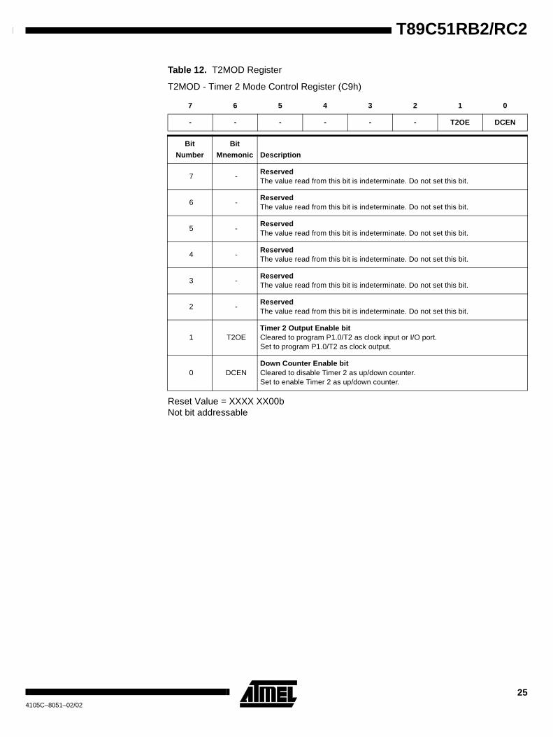
Table 12. T2MOD Register
T2MOD - Timer 2 Mode Control Register (C9h)
Reset Value = XXXX XX00bNot bit addressable
7 6 5 4 3 2 1 0
- - - - - - T2OE DCEN
Bit
Number
Bit
Mnemonic Description
7 -ReservedThe value read from this bit is indeterminate. Do not set this bit.
6 -ReservedThe value read from this bit is indeterminate. Do not set this bit.
5 -ReservedThe value read from this bit is indeterminate. Do not set this bit.
4 -ReservedThe value read from this bit is indeterminate. Do not set this bit.
3 -ReservedThe value read from this bit is indeterminate. Do not set this bit.
2 -ReservedThe value read from this bit is indeterminate. Do not set this bit.
1 T2OETimer 2 Output Enable bitCleared to program P1.0/T2 as clock input or I/O port.Set to program P1.0/T2 as clock output.
0 DCENDown Counter Enable bitCleared to disable Timer 2 as up/down counter.Set to enable Timer 2 as up/down counter.
26 T89C51RB2/RC24105C–8051–02/02
ProgrammableCounter Array PCA
The PCA provides more timing capabilities with less CPU intervention than the standardtimer/counters. Its advantages include reduced software overhead and improved accu-racy. The PCA consists of a dedicated timer/counter which serves as the time base foran array of five compare/capture modules. Its clock input can be programmed to countany one of the following signals:
• Peripheral clock frequency (FCLK PERIPH) ÷ 6
• Peripheral clock frequency (FCLK PERIPH) ÷ 2
• Timer 0 overflow
• External input on ECI (P1.2)
Each compare/capture modules can be programmed in any one of the following modes:
• rising and/or falling edge capture
• software timer
• high-speed output
• pulse width modulator
Module 4 can also be programmed as a watchdog timer (See Section "PCA WatchdogTimer", page 37).
When the compare/capture modules are programmed in the capture mode, softwaretimer, or high speed output mode, an interrupt can be generated when the module exe-cutes its function. All five modules plus the PCA timer overflow share one interruptvector.
The PCA timer/counter and compare/capture modules share Port 1 for external I/O.These pins are listed below. If the port is not used for the PCA, it can still be used forstandard I/O.
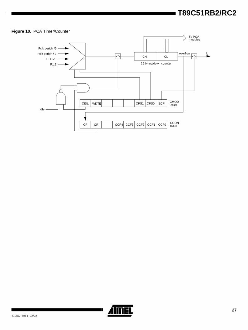
The PCA timer is a common time base for all five modules (See Figure 10). The timercount source is determined from the CPS1 and CPS0 bits in the CMOD register(Table 13) and can be programmed to run at:
• 1/6 the peripheral clock frequency (FCLK PERIPH)• 1/2 the peripheral clock frequency (FCLK PERIPH)• The Timer 0 overflow
• The input on the ECI pin (P1.2)
PCA component External I/O Pin
16-bit Counter P1.2 / ECI
16-bit Module 0 P1.3 / CEX0
16-bit Module 1 P1.4 / CEX1
16-bit Module 2 P1.5 / CEX2
16-bit Module 3 P1.6 / CEX3
27
T89C51RB2/RC2
4105C–8051–02/02
Figure 10. PCA Timer/Counter
CIDL CPS1 CPS0 ECF
ItCH CL
16 bit up/down counter
To PCAmodules
Fclk periph /6
Fclk periph / 2
T0 OVF
P1.2
Idle
CMOD0xD9WDTE
CF CRCCON0xD8CCF4 CCF3 CCF2 CCF1 CCF0
overflow
28 T89C51RB2/RC24105C–8051–02/02
Registers Table 13. CMOD Register
CMOD - PCA Counter Mode Register (D9h)
Reset Value = 00XX X000bNot bit addressable
The CMOD register includes three additional bits associated with the PCA (SeeFigure 10 and Table 13).
• The CIDL bit which allows the PCA to stop during idle mode.
• The WDTE bit which enables or disables the watchdog function on module 4.
• The ECF bit which when set causes an interrupt and the PCA overflow flag CF (inthe CCON SFR) to be set when the PCA timer overflows.
The CCON register contains the run control bit for the PCA and the flags for the PCAtimer (CF) and each module (Refer to Table 14).
• Bit CR (CCON. 6) must be set by software to run the PCA. The PCA is shut off byclearing this bit.
• Bit CF: The CF bit (CCON. 7) is set when the PCA counter overflows and aninterrupt will be generated if the ECF bit in the CMOD register is set. The CF bit canonly be cleared by software.
• Bits 0 through 4 are the flags for the modules (bit 0 for module 0, bit 1 for module 1,etc. ) and are set by hardware when either a match or a capture occurs. These flagsalso can only be cleared by software.
7 6 5 4 3 2 1 0
CIDL WDTE - - - CPS1 CPS0 ECF
Bit
Number
Bit
Mnemonic Description
7 CIDL
Counter Idle Control
Cleared to program the PCA Counter to continue functioning during idle Mode.
Set to program PCA to be gated off during idle.
6 WDTE
Watchdog Timer Enable
Cleared to disable Watchdog Timer function on PCA Module 4.
Set to enable Watchdog Timer function on PCA Module 4.
5 -Reserved
The value read from this bit is indeterminate. Do not set this bit.
4 -Reserved
The value read from this bit is indeterminate. Do not set this bit.
3 -Reserved
The value read from this bit is indeterminate. Do not set this bit.
2 CPS1 PCA Count Pulse Select
CPS1 CPS0 Selected PCA input0 0 Internal clock fCLK PERIPH/6
0 1 Internal clock fCLK PERIPH/2
1 0 Timer 0 Overflow
1 1 External clock at ECI/P1.2 pin (max rate = fCLK PERIPH/ 4)
1 CPS0
0 ECFPCA Enable Counter Overflow Interrupt
Cleared to disable CF bit in CCON to inhibit an interrupt.Set to enable CF bit in CCON to generate an interrupt.
29
T89C51RB2/RC2
4105C–8051–02/02
Table 14. CCON Register
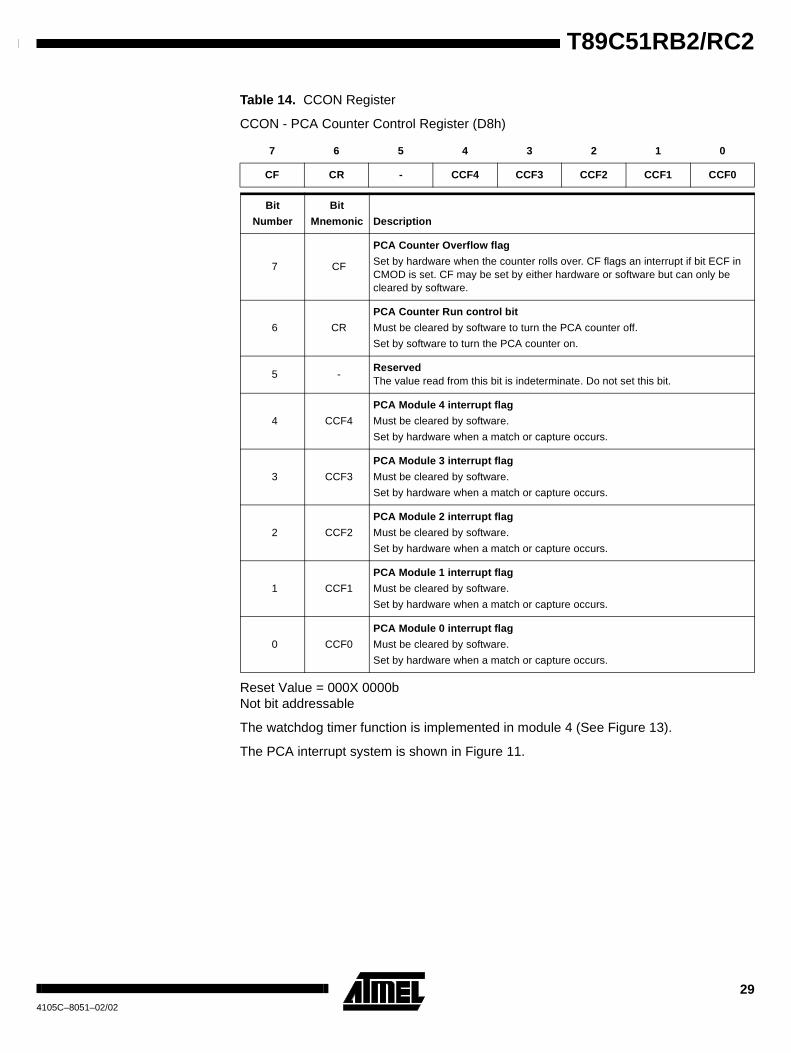
CCON - PCA Counter Control Register (D8h)
Reset Value = 000X 0000bNot bit addressable
The watchdog timer function is implemented in module 4 (See Figure 13).
The PCA interrupt system is shown in Figure 11.
7 6 5 4 3 2 1 0
CF CR - CCF4 CCF3 CCF2 CCF1 CCF0
Bit
Number
Bit
Mnemonic Description
7 CF
PCA Counter Overflow flag
Set by hardware when the counter rolls over. CF flags an interrupt if bit ECF inCMOD is set. CF may be set by either hardware or software but can only becleared by software.
6 CR
PCA Counter Run control bit
Must be cleared by software to turn the PCA counter off.
Set by software to turn the PCA counter on.
5 -ReservedThe value read from this bit is indeterminate. Do not set this bit.
4 CCF4
PCA Module 4 interrupt flag
Must be cleared by software.
Set by hardware when a match or capture occurs.
3 CCF3
PCA Module 3 interrupt flag
Must be cleared by software.
Set by hardware when a match or capture occurs.
2 CCF2
PCA Module 2 interrupt flag
Must be cleared by software.
Set by hardware when a match or capture occurs.
1 CCF1
PCA Module 1 interrupt flag
Must be cleared by software.
Set by hardware when a match or capture occurs.
0 CCF0
PCA Module 0 interrupt flag
Must be cleared by software.
Set by hardware when a match or capture occurs.
30 T89C51RB2/RC24105C–8051–02/02
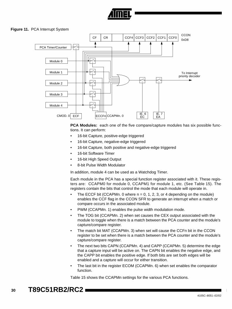
Figure 11. PCA Interrupt System
PCA Modules: each one of the five compare/capture modules has six possible func-tions. It can perform:
• 16-bit Capture, positive-edge triggered
• 16-bit Capture, negative-edge triggered
• 16-bit Capture, both positive and negative-edge triggered
• 16-bit Software Timer
• 16-bit High Speed Output
• 8-bit Pulse Width Modulator
In addition, module 4 can be used as a Watchdog Timer.
Each module in the PCA has a special function register associated with it. These regis-ters are: CCAPM0 for module 0, CCAPM1 for module 1, etc. (See Table 15). Theregisters contain the bits that control the mode that each module will operate in.
• The ECCF bit (CCAPMn. 0 where n = 0, 1, 2, 3, or 4 depending on the module)enables the CCF flag in the CCON SFR to generate an interrupt when a match orcompare occurs in the associated module.
• PWM (CCAPMn. 1) enables the pulse width modulation mode.
• The TOG bit (CCAPMn. 2) when set causes the CEX output associated with themodule to toggle when there is a match between the PCA counter and the module'scapture/compare register.
• The match bit MAT (CCAPMn. 3) when set will cause the CCFn bit in the CCONregister to be set when there is a match between the PCA counter and the module'scapture/compare register.
• The next two bits CAPN (CCAPMn. 4) and CAPP (CCAPMn. 5) determine the edgethat a capture input will be active on. The CAPN bit enables the negative edge, andthe CAPP bit enables the positive edge. If both bits are set both edges will beenabled and a capture will occur for either transition.
• The last bit in the register ECOM (CCAPMn. 6) when set enables the comparatorfunction.
Table 15 shows the CCAPMn settings for the various PCA functions.
CF CRCCON
0xD8CCF4 CCF3 CCF2 CCF1 CCF0
Module 4
Module 3
Module 2
Module 1
Module 0
ECF
PCA Timer/Counter
ECCFn CCAPMn. 0CMOD. 0IE. 6 IE. 7
To Interruptpriority decoder
EC EA
31
T89C51RB2/RC2
4105C–8051–02/02
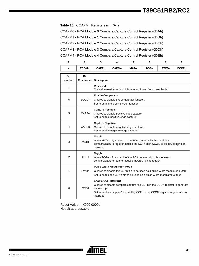
Table 15. CCAPMn Registers (n = 0-4)
CCAPM0 - PCA Module 0 Compare/Capture Control Register (0DAh)
CCAPM1 - PCA Module 1 Compare/Capture Control Register (0DBh)
CCAPM2 - PCA Module 2 Compare/Capture Control Register (0DCh)
CCAPM3 - PCA Module 3 Compare/Capture Control Register (0DDh)
CCAPM4 - PCA Module 4 Compare/Capture Control Register (0DEh)
Reset Value = X000 0000bNot bit addressable
7 6 5 4 3 2 1 0
- ECOMn CAPPn CAPNn MATn TOGn PWMn ECCFn
Bit
Number
Bit
Mnemonic Description
7 -ReservedThe value read from this bit is indeterminate. Do not set this bit.
6 ECOMn
Enable Comparator
Cleared to disable the comparator function.
Set to enable the comparator function.
5 CAPPnCapture Positive
Cleared to disable positive edge capture.Set to enable positive edge capture.
4 CAPNnCapture Negative
Cleared to disable negative edge capture.Set to enable negative edge capture.
3 MATn
Match
When MATn = 1, a match of the PCA counter with this module'scompare/capture register causes the CCFn bit in CCON to be set, flagging aninterrupt.
2 TOGnToggle
When TOGn = 1, a match of the PCA counter with this module'scompare/capture register causes theCEXn pin to toggle.
1 PWMn
Pulse Width Modulation Mode
Cleared to disable the CEXn pin to be used as a pulse width modulated output.
Set to enable the CEXn pin to be used as a pulse width modulated output.
0 CCF0
Enable CCF interrupt
Cleared to disable compare/capture flag CCFn in the CCON register to generatean interrupt.
Set to enable compare/capture flag CCFn in the CCON register to generate aninterrupt.
32 T89C51RB2/RC24105C–8051–02/02
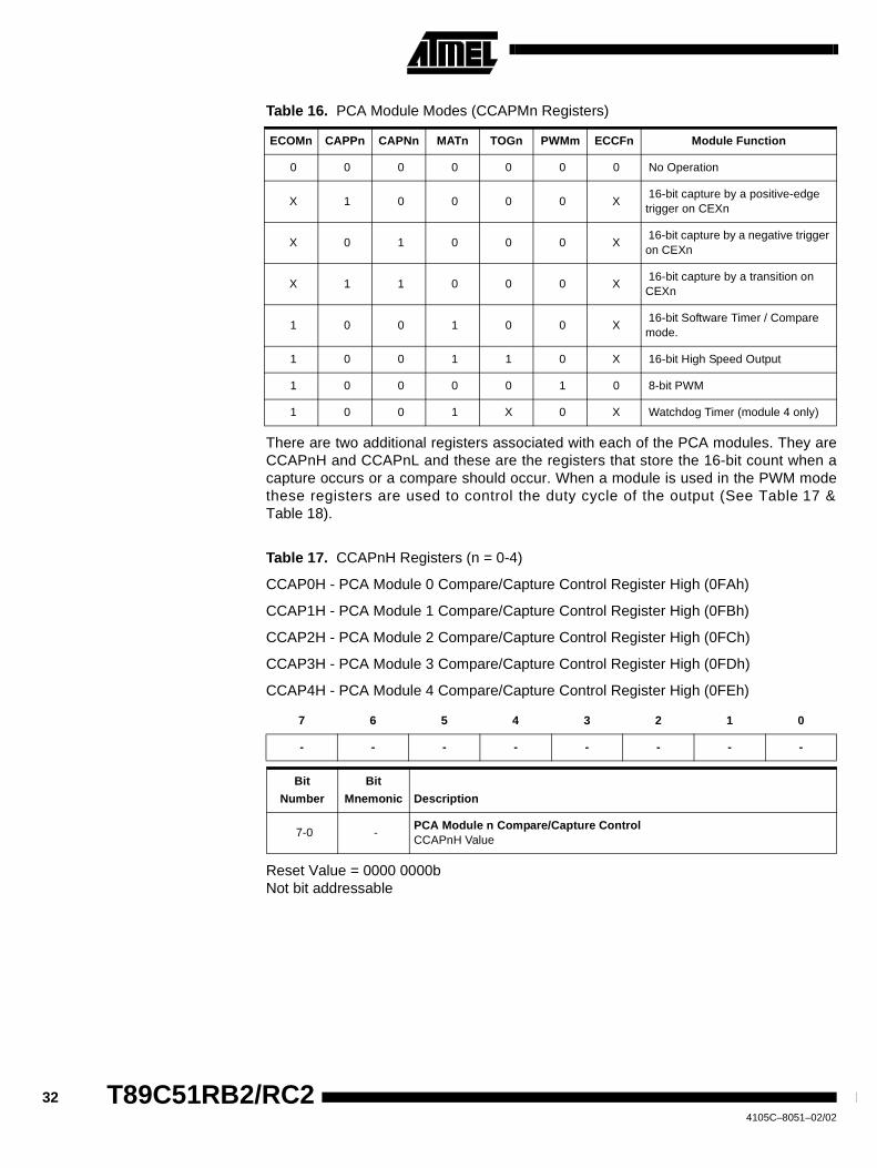
Table 16. PCA Module Modes (CCAPMn Registers)
There are two additional registers associated with each of the PCA modules. They areCCAPnH and CCAPnL and these are the registers that store the 16-bit count when acapture occurs or a compare should occur. When a module is used in the PWM modethese registers are used to control the duty cycle of the output (See Table 17 &Table 18).
Table 17. CCAPnH Registers (n = 0-4)
CCAP0H - PCA Module 0 Compare/Capture Control Register High (0FAh)
CCAP1H - PCA Module 1 Compare/Capture Control Register High (0FBh)
CCAP2H - PCA Module 2 Compare/Capture Control Register High (0FCh)
CCAP3H - PCA Module 3 Compare/Capture Control Register High (0FDh)
CCAP4H - PCA Module 4 Compare/Capture Control Register High (0FEh)
Reset Value = 0000 0000bNot bit addressable
ECOMn CAPPn CAPNn MATn TOGn PWMm ECCFn Module Function
0 0 0 0 0 0 0 No Operation
X 1 0 0 0 0 X16-bit capture by a positive-edgetrigger on CEXn
X 0 1 0 0 0 X16-bit capture by a negative triggeron CEXn
X 1 1 0 0 0 X16-bit capture by a transition onCEXn
1 0 0 1 0 0 X16-bit Software Timer / Comparemode.
1 0 0 1 1 0 X 16-bit High Speed Output
1 0 0 0 0 1 0 8-bit PWM
1 0 0 1 X 0 X Watchdog Timer (module 4 only)
7 6 5 4 3 2 1 0
- - - - - - - -
Bit
Number
Bit
Mnemonic Description
7-0 -PCA Module n Compare/Capture ControlCCAPnH Value
33
T89C51RB2/RC2
4105C–8051–02/02
Table 18. CCAPnL Registers (n = 0-4)
CCAP0L - PCA Module 0 Compare/Capture Control Register Low (0EAh)
CCAP1L - PCA Module 1 Compare/Capture Control Register Low (0EBh)
CCAP2L - PCA Module 2 Compare/Capture Control Register Low (0ECh)
CCAP3L - PCA Module 3 Compare/Capture Control Register Low (0EDh)
CCAP4L - PCA Module 4 Compare/Capture Control Register Low (0EEh)
Reset Value = 0000 0000bNot bit addressable
Table 19. CH Register
CH - PCA Counter Register High (0F9h)
Reset Value = 0000 0000bNot bit addressable
Table 20. CL Register
CL - PCA Counter Register Low (0E9h)
Reset Value = 0000 0000bNot bit addressable
7 6 5 4 3 2 1 0
- - - - - - - -
Bit
Number
Bit
Mnemonic Description
7-0 -PCA Module n Compare/Capture ControlCCAPnL Value
7 6 5 4 3 2 1 0
- - - - - - - -
Bit
Number
Bit
Mnemonic Description
7-0 -PCA counterCH Value
7 6 5 4 3 2 1 0
- - - - - - - -
Bit
Number
Bit
Mnemonic Description
7-0 -PCA CounterCL Value
34 T89C51RB2/RC24105C–8051–02/02
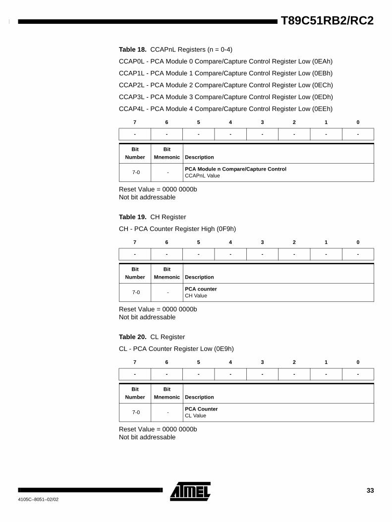
PCA Capture Mode To use one of the PCA modules in the capture mode either one or both of the CCAPMbits CAPN and CAPP for that module must be set. The external CEX input for the mod-ule (on port 1) is sampled for a transition. When a valid transition occurs the PCAhardware loads the value of the PCA counter registers (CH and CL) into the module'scapture registers (CCAPnL and CCAPnH). If the CCFn bit for the module in the CCONSFR and the ECCFn bit in the CCAPMn SFR are set then an interrupt will be generated(Refer to Figure 12).
Figure 12. PCA Capture Mode
CF CR CCON0xD8
CH CL
CCAPnH CCAPnL
CCF4 CCF3 CCF2 CCF1 CCF0
PCA IT
PCA Counter/Timer
ECOMn CCAPMn, n= 0 to 40xDA to 0xDE
CAPNn MATn TOGn PWMn ECCFnCAPPn
Cex. n
Capture
35
T89C51RB2/RC2
4105C–8051–02/02
16-bit Software Timer/Compare Mode
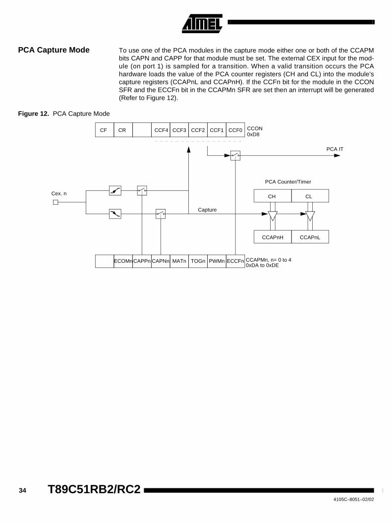
The PCA modules can be used as software timers by setting both the ECOM and MATbits in the modules CCAPMn register. The PCA timer will be compared to the module'scapture registers and when a match occurs, an interrupt will occur if the CCFn (CCONSFR) and the ECCFn (CCAPMn SFR) bits for the module are both set (See Figure 13).
Figure 13. PCA Compare Mode and PCA Watchdog Timer
Before enabling ECOM bit, CCAPnL and CCAPnH should be set with a non zero value,otherwise an unwanted match could happen. Writing to CCAPnH will set the ECOM bit.
Once ECOM set, writing CCAPnL will clear ECOM so that an unwanted match doesn’toccur while modifying the compare value. Writing to CCAPnH will set ECOM. For thisreason, user software should write CCAPnL first, and then CCAPnH. Of course, theECOM bit can still be controlled by accessing to CCAPMn register.
CH CL
CCAPnH CCAPnL
ECOMnCCAPMn, n = 0 to 4
0xDA to 0xDECAPNn MATn TOGn PWMn ECCFnCAPPn
16 bit comparatorMatch
CCON
0xD8
PCA IT
Enable
PCA counter/timer
RESET *
CIDL CPS1 CPS0 ECFCMOD
0xD9WDTE
* Only for Module 4
ResetWrite toCCAPnL
Write toCCAPnH
CF CCF2 CCF1 CCF0CR CCF3CCF4
1 0
36 T89C51RB2/RC24105C–8051–02/02
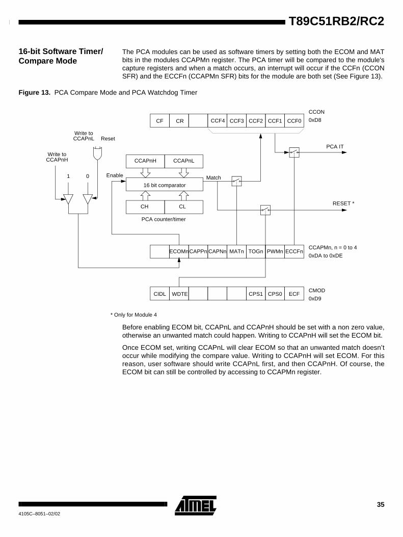
High Speed Output Mode In this mode the CEX output (on port 1) associated with the PCA module will toggleeach time a match occurs between the PCA counter and the module's capture registers.To activate this mode the TOG, MAT, and ECOM bits in the module's CCAPMn SFRmust be set (See Figure 14).
A prior write must be done to CCAPnL and CCAPnH before writing the ECOMn bit.
Figure 14. PCA High Speed Output Mode
Before enabling ECOM bit, CCAPnL and CCAPnH should be set with a non zero value,otherwise an unwanted match could happen.
Once ECOM set, writing CCAPnL will clear ECOM so that an unwanted match doesn’toccur while modifying the compare value. Writing to CCAPnH will set ECOM. For thisreason, user software should write CCAPnL first, and then CCAPnH. Of course, theECOM bit can still be controlled by accessing to CCAPMn register.
CH CL
CCAPnH CCAPnL
ECOMnCCAPMn, n = 0 to 4
0xDA to 0xDECAPNn MATn TOGn PWMn ECCFnCAPPn
16 bit comparatorMatch
CF CRCCON
0xD8CCF4 CCF3 CCF2 CCF1 CCF0
PCA IT
Enable
CEXn
PCA counter/timer
Write toCCAPnH
ResetWrite toCCAPnL
1 0
37
T89C51RB2/RC2
4105C–8051–02/02
Pulse Width ModulatorMode
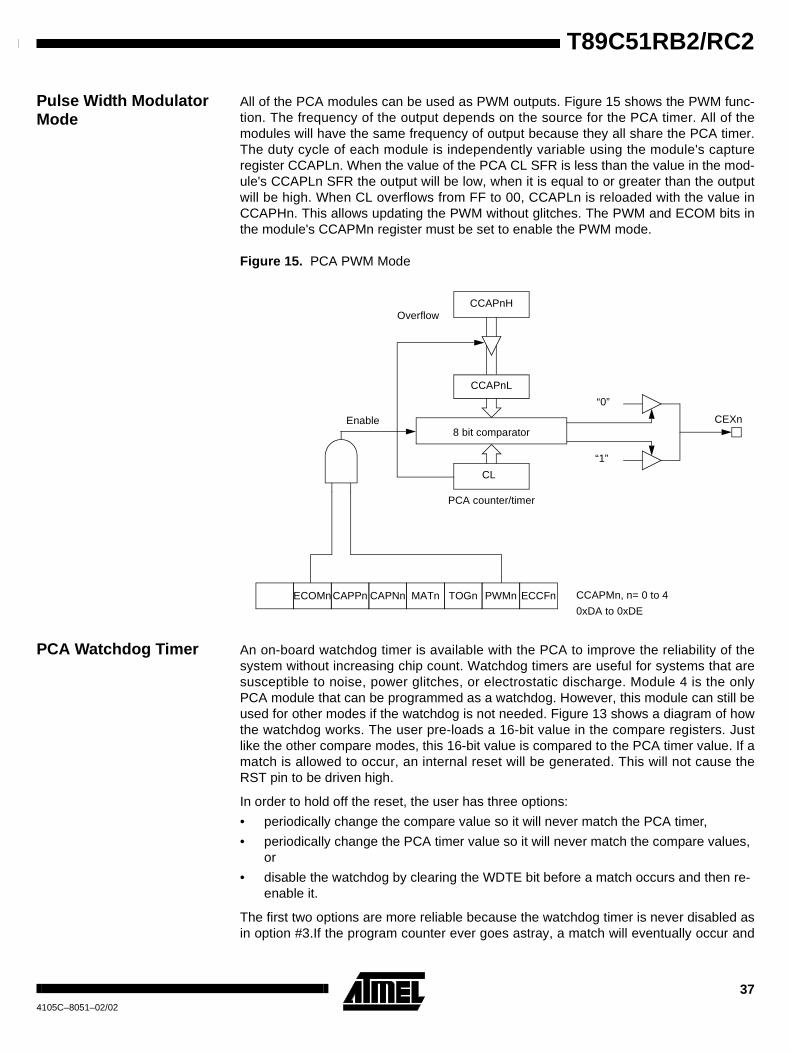
All of the PCA modules can be used as PWM outputs. Figure 15 shows the PWM func-tion. The frequency of the output depends on the source for the PCA timer. All of themodules will have the same frequency of output because they all share the PCA timer.The duty cycle of each module is independently variable using the module's captureregister CCAPLn. When the value of the PCA CL SFR is less than the value in the mod-ule's CCAPLn SFR the output will be low, when it is equal to or greater than the outputwill be high. When CL overflows from FF to 00, CCAPLn is reloaded with the value inCCAPHn. This allows updating the PWM without glitches. The PWM and ECOM bits inthe module's CCAPMn register must be set to enable the PWM mode.
Figure 15. PCA PWM Mode
PCA Watchdog Timer An on-board watchdog timer is available with the PCA to improve the reliability of thesystem without increasing chip count. Watchdog timers are useful for systems that aresusceptible to noise, power glitches, or electrostatic discharge. Module 4 is the onlyPCA module that can be programmed as a watchdog. However, this module can still beused for other modes if the watchdog is not needed. Figure 13 shows a diagram of howthe watchdog works. The user pre-loads a 16-bit value in the compare registers. Justlike the other compare modes, this 16-bit value is compared to the PCA timer value. If amatch is allowed to occur, an internal reset will be generated. This will not cause theRST pin to be driven high.
In order to hold off the reset, the user has three options:
• periodically change the compare value so it will never match the PCA timer,
• periodically change the PCA timer value so it will never match the compare values,or
• disable the watchdog by clearing the WDTE bit before a match occurs and then re-enable it.
The first two options are more reliable because the watchdog timer is never disabled asin option #3.If the program counter ever goes astray, a match will eventually occur and
CL
CCAPnH
CCAPnL
ECOMn CCAPMn, n= 0 to 4
0xDA to 0xDE
CAPNn MATn TOGn PWMn ECCFnCAPPn
8 bit comparatorCEXn
“0”
“1”
Enable
PCA counter/timer
Overflow

38 T89C51RB2/RC24105C–8051–02/02
cause an internal reset. The second option is also not recommended if other PCA mod-ules are being used. Remember, the PCA timer is the time base for all modules;changing the time base for other modules would not be a good idea. Thus, in most appli-cations the first solution is the best option.
This watchdog timer won’t generate a reset out on the reset pin.
39
T89C51RB2/RC2
4105C–8051–02/02
Serial I/O Port The serial I/O port in the T89C51RB2/RC2 is compatible with the serial I/O port in the80C52.It provides both synchronous and asynchronous communication modes. It operates as aUniversal Asynchronous Receiver and Transmitter (UART) in three full-duplex modes(Modes 1, 2 and 3). Asynchronous transmission and reception can occur simultaneouslyand at different baud rates
Serial I/O port includes the following enhancements:
• Framing error detection
• Automatic address recognition
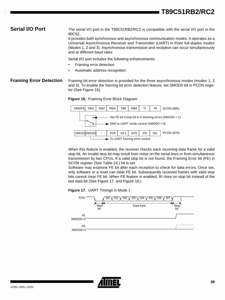
Framing Error Detection Framing bit error detection is provided for the three asynchronous modes (modes 1, 2and 3). To enable the framing bit error detection feature, set SMOD0 bit in PCON regis-ter (See Figure 16).
Figure 16. Framing Error Block Diagram
When this feature is enabled, the receiver checks each incoming data frame for a validstop bit. An invalid stop bit may result from noise on the serial lines or from simultaneoustransmission by two CPUs. If a valid stop bit is not found, the Framing Error bit (FE) inSCON register (See Table 24.) bit is set.Software may examine FE bit after each reception to check for data errors. Once set,only software or a reset can clear FE bit. Subsequently received frames with valid stopbits cannot clear FE bit. When FE feature is enabled, RI rises on stop bit instead of thelast data bit (See Figure 17. and Figure 18.).
Figure 17. UART Timings in Mode 1
RITIRB8TB8RENSM2SM1SM0/FE
IDLPDGF0GF1POF-SMOD0SMOD1
To UART framing error control
SM0 to UART mode control (SMOD0 = 0)
Set FE bit if stop bit is 0 (framing error) (SMOD0 = 1)
SCON (98h)
PCON (87h)
Data byte
RISMOD0=X
Stopbit
Startbit
RXD D7D6D5D4D3D2D1D0
FESMOD0=1
40 T89C51RB2/RC24105C–8051–02/02
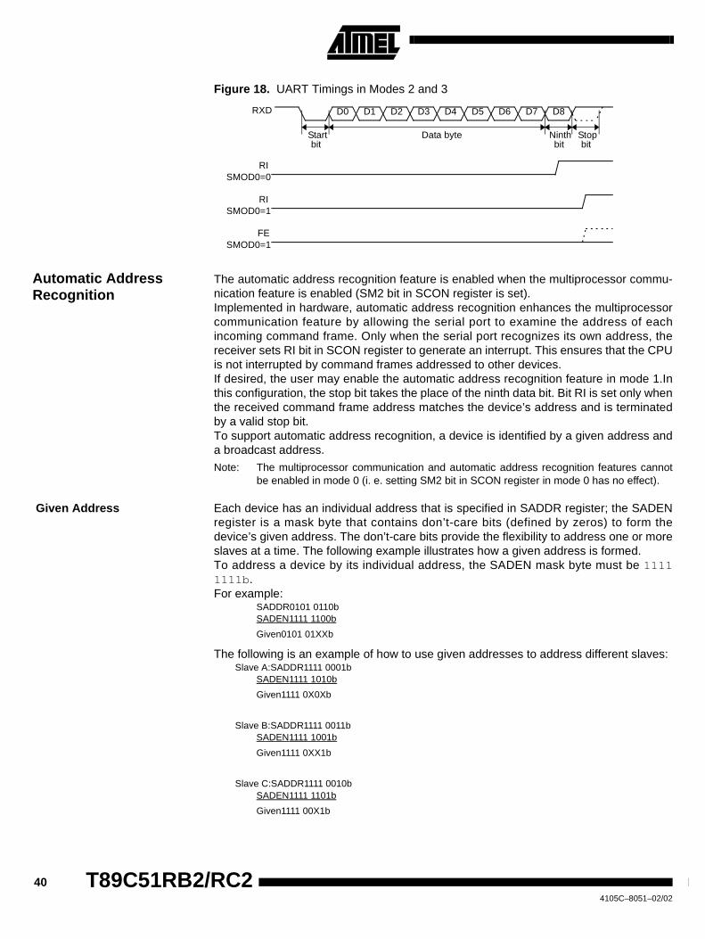
Figure 18. UART Timings in Modes 2 and 3
Automatic AddressRecognition
The automatic address recognition feature is enabled when the multiprocessor commu-nication feature is enabled (SM2 bit in SCON register is set).Implemented in hardware, automatic address recognition enhances the multiprocessorcommunication feature by allowing the serial port to examine the address of eachincoming command frame. Only when the serial port recognizes its own address, thereceiver sets RI bit in SCON register to generate an interrupt. This ensures that the CPUis not interrupted by command frames addressed to other devices.If desired, the user may enable the automatic address recognition feature in mode 1.Inthis configuration, the stop bit takes the place of the ninth data bit. Bit RI is set only whenthe received command frame address matches the device’s address and is terminatedby a valid stop bit.To support automatic address recognition, a device is identified by a given address anda broadcast address.
Note: The multiprocessor communication and automatic address recognition features cannotbe enabled in mode 0 (i. e. setting SM2 bit in SCON register in mode 0 has no effect).
Given Address Each device has an individual address that is specified in SADDR register; the SADENregister is a mask byte that contains don’t-care bits (defined by zeros) to form thedevice’s given address. The don’t-care bits provide the flexibility to address one or moreslaves at a time. The following example illustrates how a given address is formed.To address a device by its individual address, the SADEN mask byte must be 11111111b.For example:
SADDR0101 0110bSADEN1111 1100b
Given0101 01XXb
The following is an example of how to use given addresses to address different slaves:Slave A:SADDR1111 0001b
SADEN1111 1010b
Given1111 0X0Xb
Slave B:SADDR1111 0011bSADEN1111 1001b
Given1111 0XX1b
Slave C:SADDR1111 0010bSADEN1111 1101b
Given1111 00X1b
RISMOD0=0
Data byte Ninthbit
Stopbit
Startbit
RXD D8D7D6D5D4D3D2D1D0
RISMOD0=1
FESMOD0=1
41
T89C51RB2/RC2
4105C–8051–02/02
The SADEN byte is selected so that each slave may be addressed separately.For slave A, bit 0 (the LSB) is a don’t-care bit; for slaves B and C, bit 0 is a 1.To commu-nicate with slave A only, the master must send an address where bit 0 is clear (e. g.1111 0000b).For slave A, bit 1 is a 1; for slaves B and C, bit 1 is a don’t care bit. To communicate withslaves B and C, but not slave A, the master must send an address with bits 0 and 1 bothset (e. g. 1111 0011b).To communicate with slaves A, B and C, the master must send an address with bit 0 set,bit 1 clear, and bit 2 clear (e. g. 1111 0001b).
Broadcast Address A broadcast address is formed from the logical OR of the SADDR and SADEN registerswith zeros defined as don’t-care bits, e. g. :
SADDR0101 0110bSADEN1111 1100b
Broadcast =SADDR OR SADEN1111 111Xb
The use of don’t-care bits provides flexibility in defining the broadcast address, howeverin most applications, a broadcast address is FFh. The following is an example of usingbroadcast addresses:
Slave A:SADDR1111 0001bSADEN1111 1010b
Broadcast1111 1X11b,
Slave B:SADDR1111 0011bSADEN1111 1001b
Broadcast1111 1X11B,
Slave C:SADDR=1111 0010bSADEN1111 1101b
Broadcast1111 1111b
For slaves A and B, bit 2 is a don’t care bit; for slave C, bit 2 is set. To communicate withall of the slaves, the master must send an address FFh. To communicate with slaves Aand B, but not slave C, the master can send and address FBh.
Reset Addresses On reset, the SADDR and SADEN registers are initialized to 00h, i. e. the given andbroadcast addresses are XXXX XXXXb (all don’t-care bits). This ensures that the serialport will reply to any address, and so, that it is backwards compatible with the 80C51microcontrollers that do not support automatic address recognition.
42 T89C51RB2/RC24105C–8051–02/02
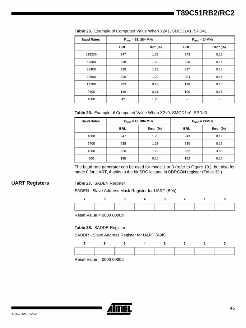
Registers Table 21. SADEN Register
SADEN - Slave Address Mask Register (B9h)
Reset Value = 0000 0000bNot bit addressable
Table 22. SADDR Register
SADDR - Slave Address Register (A9h)
Reset Value = 0000 0000bNot bit addressable
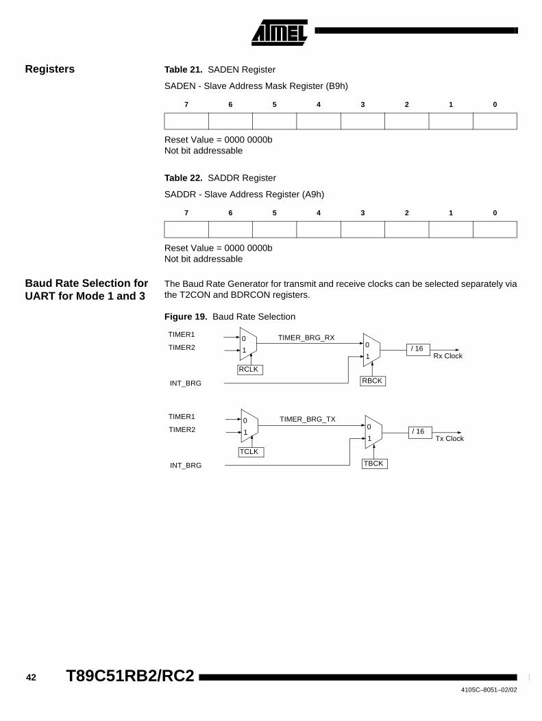
Baud Rate Selection forUART for Mode 1 and 3
The Baud Rate Generator for transmit and receive clocks can be selected separately viathe T2CON and BDRCON registers.
Figure 19. Baud Rate Selection
7 6 5 4 3 2 1 0
7 6 5 4 3 2 1 0
RCLK
/ 16
RBCKINT_BRG
0
1
TIMER1
0
1
0
1TIMER2
INT_BRG
TIMER1
TIMER2
TIMER_BRG_RX
Rx Clock
/ 160
1
TIMER_BRG_TX
Tx Clock
TBCK
TCLK
43
T89C51RB2/RC2
4105C–8051–02/02
Table 23. Baud Rate Selection Table UART
Internal Baud Rate Generator(BRG)
When the internal Baud Rate Generator is used, the Baud Rates are determined by theBRG overflow depending on the BRL reload value, the value of SPD bit (Speed Mode)in BDRCON register and the value of the SMOD1 bit in PCON register.
Figure 20. Internal Baud Rate
• The baud rate for UART is token by formula:
TCLK
(T2CON)
RCLK
(T2CON)
TBCK
(BDRCON)
RBCK
(BDRCON)
Clock Source
UART Tx
Clock Source
UART Rx
0 0 0 0 Timer 1 Timer 1
1 0 0 0 Timer 2 Timer 1
0 1 0 0 Timer 1 Timer 2
1 1 0 0 Timer 2 Timer 2
X 0 1 0 INT_BRG Timer 1
X 1 1 0 INT_BRG Timer 2
0 X 0 1 Timer 1 INT_BRG
1 X 0 1 Timer 2 INT_BRG
X X 1 1 INT_BRG INT_BRG
BRG0
1
/6
BRL
/2
0
1INT_BRG
SPD
BRR
SMOD1
auto reload counteroverflowCLK PERIPH
Baud_Rate =2SMOD1 x FCLK PERIPH
2 x 2 x 6(1-SPD) x 16 x [256 - (BRL)]
(BRL) = 256 -2SMOD1 x FCLK PERIPH
2 x 2 x 6(1-SPD) x 16 x Baud_Rate
44 T89C51RB2/RC24105C–8051–02/02
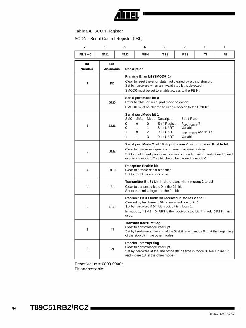
Table 24. SCON Register
SCON - Serial Control Register (98h)
Reset Value = 0000 0000bBit addressable
7 6 5 4 3 2 1 0
FE/SM0 SM1 SM2 REN TB8 RB8 TI RI
Bit
Number
Bit
Mnemonic Description
7 FE
Framing Error bit (SMOD0=1)
Clear to reset the error state, not cleared by a valid stop bit.Set by hardware when an invalid stop bit is detected.
SMOD0 must be set to enable access to the FE bit.
SM0Serial port Mode bit 0Refer to SM1 for serial port mode selection.
SMOD0 must be cleared to enable access to the SM0 bit.
6 SM1
Serial port Mode bit 1SM0 SM1 Mode Description Baud Rate
0 0 0 Shift Register FCPU PERIPH/60 1 1 8-bit UART Variable1 0 2 9-bit UART FCPU PERIPH /32 or /16
1 1 3 9-bit UART Variable
5 SM2
Serial port Mode 2 bit / Multiprocessor Communication Enable bit
Clear to disable multiprocessor communication feature.
Set to enable multiprocessor communication feature in mode 2 and 3, andeventually mode 1.This bit should be cleared in mode 0.
4 RENReception Enable bitClear to disable serial reception.Set to enable serial reception.
3 TB8Transmitter Bit 8 / Ninth bit to transmit in modes 2 and 3
Clear to transmit a logic 0 in the 9th bit.Set to transmit a logic 1 in the 9th bit.
2 RB8
Receiver Bit 8 / Ninth bit received in modes 2 and 3Cleared by hardware if 9th bit received is a logic 0.Set by hardware if 9th bit received is a logic 1.
In mode 1, if SM2 = 0, RB8 is the received stop bit. In mode 0 RB8 is notused.
1 TI
Transmit Interrupt flagClear to acknowledge interrupt.Set by hardware at the end of the 8th bit time in mode 0 or at the beginningof the stop bit in the other modes.
0 RI
Receive Interrupt flagClear to acknowledge interrupt.Set by hardware at the end of the 8th bit time in mode 0, see Figure 17.and Figure 18. in the other modes.
45
T89C51RB2/RC2
4105C–8051–02/02
Table 25. Example of Computed Value When X2=1, SMOD1=1, SPD=1
Table 26. Example of Computed Value When X2=0, SMOD1=0, SPD=0
The baud rate generator can be used for mode 1 or 3 (refer to Figure 19.), but also formode 0 for UART, thanks to the bit SRC located in BDRCON register (Table 33.)
UART Registers Table 27. SADEN Register
SADEN - Slave Address Mask Register for UART (B9h)
Reset Value = 0000 0000b
Table 28. SADDR Register
SADDR - Slave Address Register for UART (A9h)
Reset Value = 0000 0000b
Baud Rates FOSC = 16. 384 MHz FOSC = 24MHz
BRL Error (%) BRL Error (%)
115200 247 1.23 243 0.16
57600 238 1.23 230 0.16
38400 229 1.23 217 0.16
28800 220 1.23 204 0.16
19200 203 0.63 178 0.16
9600 149 0.31 100 0.16
4800 43 1.23 - -
Baud Rates FOSC = 16. 384 MHz FOSC = 24MHz
BRL Error (%) BRL Error (%)
4800 247 1.23 243 0.16
2400 238 1.23 230 0.16
1200 220 1.23 202 3.55
600 185 0.16 152 0.16
7 6 5 4 3 2 1 0
7 6 5 4 3 2 1 0
46 T89C51RB2/RC24105C–8051–02/02
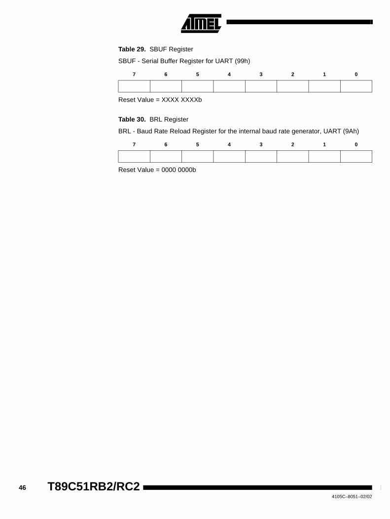
Table 29. SBUF Register
SBUF - Serial Buffer Register for UART (99h)
Reset Value = XXXX XXXXb
Table 30. BRL Register
BRL - Baud Rate Reload Register for the internal baud rate generator, UART (9Ah)
Reset Value = 0000 0000b
7 6 5 4 3 2 1 0
7 6 5 4 3 2 1 0
47
T89C51RB2/RC2
4105C–8051–02/02
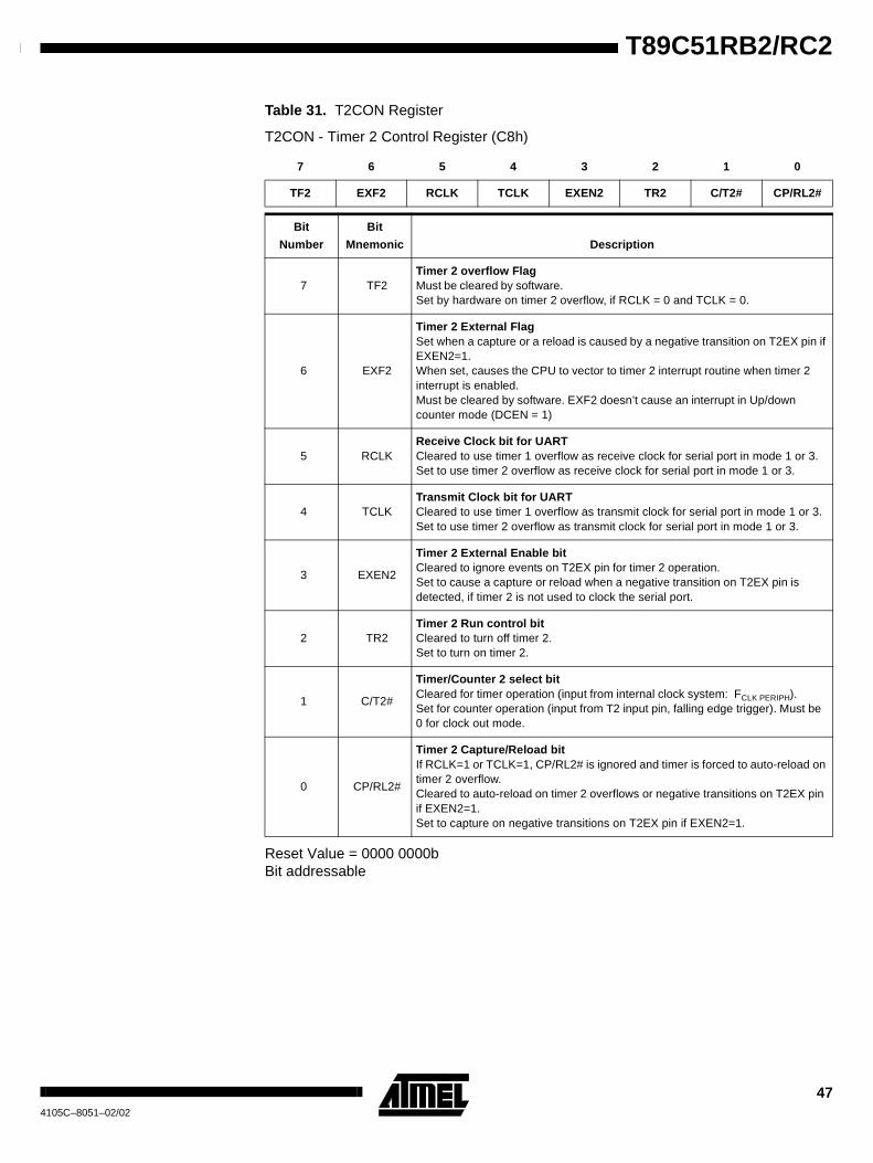
Table 31. T2CON Register
T2CON - Timer 2 Control Register (C8h)
Reset Value = 0000 0000bBit addressable
7 6 5 4 3 2 1 0
TF2 EXF2 RCLK TCLK EXEN2 TR2 C/T2# CP/RL2#
Bit
Number
Bit
Mnemonic Description
7 TF2Timer 2 overflow FlagMust be cleared by software.Set by hardware on timer 2 overflow, if RCLK = 0 and TCLK = 0.
6 EXF2
Timer 2 External FlagSet when a capture or a reload is caused by a negative transition on T2EX pin ifEXEN2=1.When set, causes the CPU to vector to timer 2 interrupt routine when timer 2interrupt is enabled.Must be cleared by software. EXF2 doesn’t cause an interrupt in Up/downcounter mode (DCEN = 1)
5 RCLKReceive Clock bit for UARTCleared to use timer 1 overflow as receive clock for serial port in mode 1 or 3.Set to use timer 2 overflow as receive clock for serial port in mode 1 or 3.
4 TCLKTransmit Clock bit for UARTCleared to use timer 1 overflow as transmit clock for serial port in mode 1 or 3.Set to use timer 2 overflow as transmit clock for serial port in mode 1 or 3.
3 EXEN2
Timer 2 External Enable bitCleared to ignore events on T2EX pin for timer 2 operation.Set to cause a capture or reload when a negative transition on T2EX pin isdetected, if timer 2 is not used to clock the serial port.
2 TR2Timer 2 Run control bitCleared to turn off timer 2.Set to turn on timer 2.
1 C/T2#
Timer/Counter 2 select bitCleared for timer operation (input from internal clock system: FCLK PERIPH).Set for counter operation (input from T2 input pin, falling edge trigger). Must be0 for clock out mode.
0 CP/RL2#
Timer 2 Capture/Reload bitIf RCLK=1 or TCLK=1, CP/RL2# is ignored and timer is forced to auto-reload ontimer 2 overflow.Cleared to auto-reload on timer 2 overflows or negative transitions on T2EX pinif EXEN2=1.Set to capture on negative transitions on T2EX pin if EXEN2=1.
48 T89C51RB2/RC24105C–8051–02/02
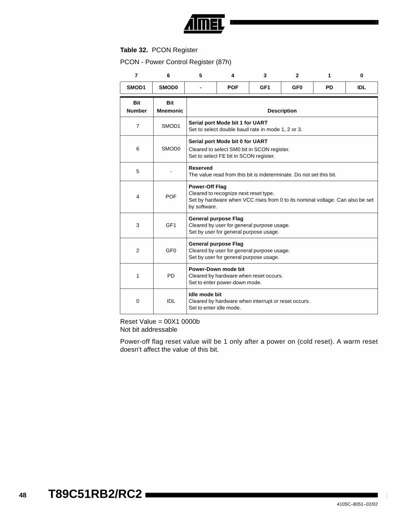
Table 32. PCON Register
PCON - Power Control Register (87h)
Reset Value = 00X1 0000bNot bit addressable
Power-off flag reset value will be 1 only after a power on (cold reset). A warm resetdoesn’t affect the value of this bit.
7 6 5 4 3 2 1 0
SMOD1 SMOD0 - POF GF1 GF0 PD IDL
Bit
Number
Bit
Mnemonic Description
7 SMOD1Serial port Mode bit 1 for UARTSet to select double baud rate in mode 1, 2 or 3.
6 SMOD0Serial port Mode bit 0 for UART
Cleared to select SM0 bit in SCON register.Set to select FE bit in SCON register.
5 -ReservedThe value read from this bit is indeterminate. Do not set this bit.
4 POF
Power-Off FlagCleared to recognize next reset type.Set by hardware when VCC rises from 0 to its nominal voltage. Can also be setby software.
3 GF1General purpose FlagCleared by user for general purpose usage.Set by user for general purpose usage.
2 GF0General purpose FlagCleared by user for general purpose usage.Set by user for general purpose usage.
1 PDPower-Down mode bitCleared by hardware when reset occurs.Set to enter power-down mode.
0 IDLIdle mode bitCleared by hardware when interrupt or reset occurs.Set to enter idle mode.
49
T89C51RB2/RC2
4105C–8051–02/02
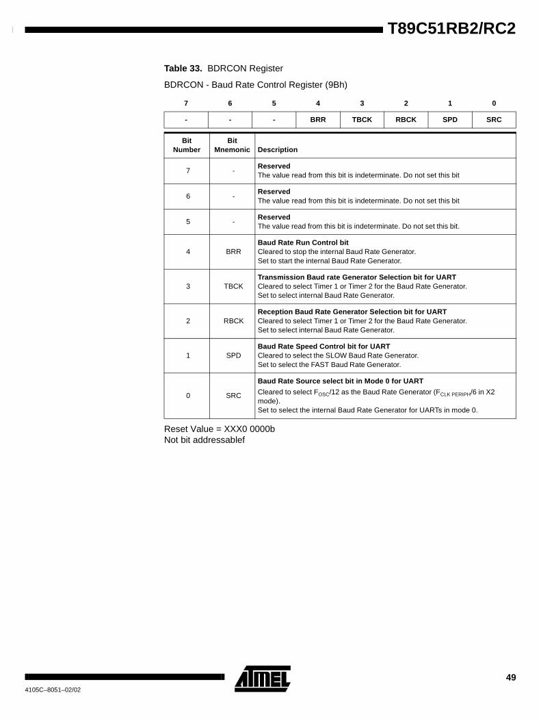
Table 33. BDRCON Register
BDRCON - Baud Rate Control Register (9Bh)
Reset Value = XXX0 0000bNot bit addressablef
7 6 5 4 3 2 1 0
- - - BRR TBCK RBCK SPD SRC
BitNumber
BitMnemonic Description
7 -ReservedThe value read from this bit is indeterminate. Do not set this bit
6 -ReservedThe value read from this bit is indeterminate. Do not set this bit
5 -ReservedThe value read from this bit is indeterminate. Do not set this bit.
4 BRRBaud Rate Run Control bitCleared to stop the internal Baud Rate Generator.Set to start the internal Baud Rate Generator.
3 TBCKTransmission Baud rate Generator Selection bit for UARTCleared to select Timer 1 or Timer 2 for the Baud Rate Generator.Set to select internal Baud Rate Generator.
2 RBCKReception Baud Rate Generator Selection bit for UARTCleared to select Timer 1 or Timer 2 for the Baud Rate Generator.Set to select internal Baud Rate Generator.
1 SPDBaud Rate Speed Control bit for UARTCleared to select the SLOW Baud Rate Generator.Set to select the FAST Baud Rate Generator.
0 SRC
Baud Rate Source select bit in Mode 0 for UART
Cleared to select FOSC/12 as the Baud Rate Generator (FCLK PERIPH/6 in X2mode).Set to select the internal Baud Rate Generator for UARTs in mode 0.
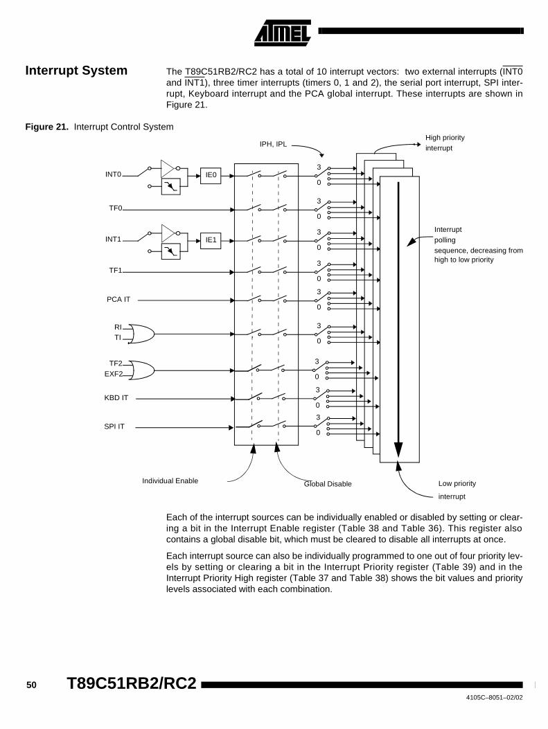
50 T89C51RB2/RC24105C–8051–02/02
Interrupt System The T89C51RB2/RC2 has a total of 10 interrupt vectors: two external interrupts (INT0and INT1), three timer interrupts (timers 0, 1 and 2), the serial port interrupt, SPI inter-rupt, Keyboard interrupt and the PCA global interrupt. These interrupts are shown inFigure 21.
Figure 21. Interrupt Control System
Each of the interrupt sources can be individually enabled or disabled by setting or clear-ing a bit in the Interrupt Enable register (Table 38 and Table 36). This register alsocontains a global disable bit, which must be cleared to disable all interrupts at once.
Each interrupt source can also be individually programmed to one out of four priority lev-els by setting or clearing a bit in the Interrupt Priority register (Table 39) and in theInterrupt Priority High register (Table 37 and Table 38) shows the bit values and prioritylevels associated with each combination.
IE1
0
3
High priorityinterrupt
Interruptpollingsequence, decreasing fromhigh to low priority
Low priority
interrupt
Global DisableIndividual Enable
EXF2TF2
TIRI
TF0
INT0
INT1
TF1
IPH, IPL
IE0
0
3
0
3
0
3
0
3
0
3
0
3
PCA IT
KBD IT
SPI IT
0
3
0
3
51
T89C51RB2/RC2
4105C–8051–02/02
Registers The PCA interrupt vector is located at address 0033H, the SPI interrupt vector is locatedat address 0043H and Keyboard interrupt vector is located at address 004BH. All othervectors addresses are the same as standard C52 devices.
Table 34. Priority Level Bit Values
A low-priority interrupt can be interrupted by a high priority interrupt, but not by anotherlow-priority interrupt. A high-priority interrupt can’t be interrupted by any other interruptsource.
If two interrupt requests of different priority levels are received simultaneously, therequest of higher priority level is serviced. If interrupt requests of the same priority levelare received simultaneously, an internal polling sequence determines which request isserviced. Thus within each priority level there is a second priority structure determinedby the polling sequence.
IPH. x IPL. x Interrupt Level Priority
0 0 0 (Lowest)
0 1 1
1 0 2
1 1 3 (Highest)
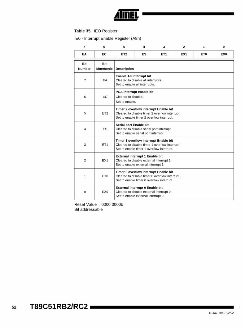
52 T89C51RB2/RC24105C–8051–02/02
Table 35. IEO Register
IE0 - Interrupt Enable Register (A8h)
Reset Value = 0000 0000bBit addressable
7 6 5 4 3 2 1 0
EA EC ET2 ES ET1 EX1 ET0 EX0
Bit
Number
Bit
Mnemonic Description
7 EAEnable All interrupt bitCleared to disable all interrupts.Set to enable all interrupts.
6 EC
PCA interrupt enable bit
Cleared to disable.
Set to enable.
5 ET2Timer 2 overflow interrupt Enable bitCleared to disable timer 2 overflow interrupt.Set to enable timer 2 overflow interrupt.
4 ESSerial port Enable bitCleared to disable serial port interrupt.Set to enable serial port interrupt.
3 ET1Timer 1 overflow interrupt Enable bitCleared to disable timer 1 overflow interrupt.Set to enable timer 1 overflow interrupt.
2 EX1External interrupt 1 Enable bitCleared to disable external interrupt 1.Set to enable external interrupt 1.
1 ET0Timer 0 overflow interrupt Enable bitCleared to disable timer 0 overflow interrupt.Set to enable timer 0 overflow interrupt.
0 EX0External interrupt 0 Enable bitCleared to disable external interrupt 0.Set to enable external interrupt 0.
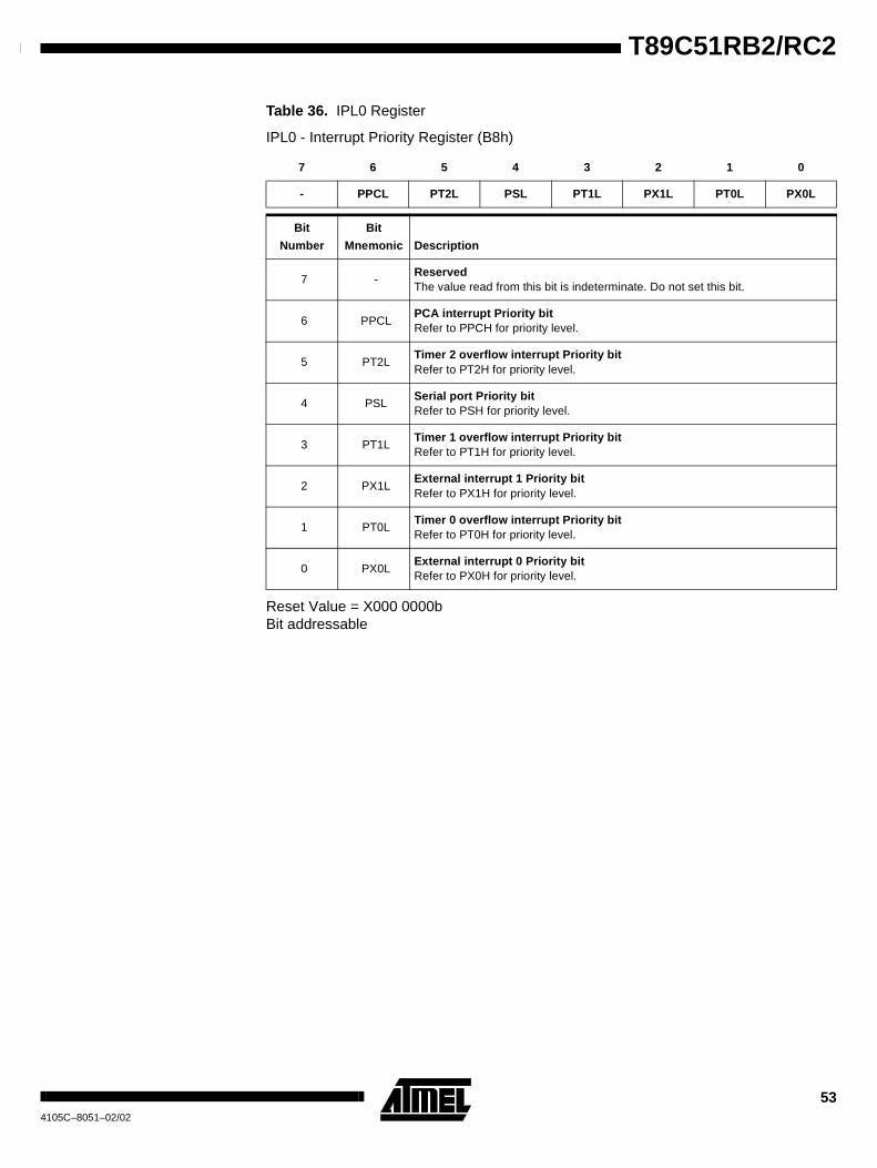
53
T89C51RB2/RC2
4105C–8051–02/02
Table 36. IPL0 Register
IPL0 - Interrupt Priority Register (B8h)
Reset Value = X000 0000bBit addressable
7 6 5 4 3 2 1 0
- PPCL PT2L PSL PT1L PX1L PT0L PX0L
Bit
Number
Bit
Mnemonic Description
7 -ReservedThe value read from this bit is indeterminate. Do not set this bit.
6 PPCLPCA interrupt Priority bitRefer to PPCH for priority level.
5 PT2LTimer 2 overflow interrupt Priority bitRefer to PT2H for priority level.
4 PSLSerial port Priority bitRefer to PSH for priority level.
3 PT1LTimer 1 overflow interrupt Priority bitRefer to PT1H for priority level.
2 PX1LExternal interrupt 1 Priority bitRefer to PX1H for priority level.
1 PT0LTimer 0 overflow interrupt Priority bitRefer to PT0H for priority level.
0 PX0LExternal interrupt 0 Priority bitRefer to PX0H for priority level.
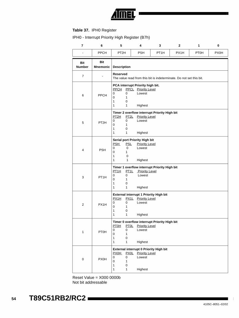
54 T89C51RB2/RC24105C–8051–02/02
Table 37. IPH0 Register
IPH0 - Interrupt Priority High Register (B7h)
Reset Value = X000 0000bNot bit addressable
7 6 5 4 3 2 1 0
- PPCH PT2H PSH PT1H PX1H PT0H PX0H
BitNumber
Bit
Mnemonic Description
7 -ReservedThe value read from this bit is indeterminate. Do not set this bit.
6 PPCH
PCA interrupt Priority high bit.PPCH PPCL Priority Level0 0 Lowest0 11 01 1 Highest
5 PT2H
Timer 2 overflow interrupt Priority High bitPT2H PT2L Priority Level0 0 Lowest0 11 01 1 Highest
4 PSH
Serial port Priority High bitPSH PSL Priority Level0 0 Lowest0 11 01 1 Highest
3 PT1H
Timer 1 overflow interrupt Priority High bitPT1H PT1L Priority Level0 0 Lowest0 11 01 1 Highest
2 PX1H
External interrupt 1 Priority High bitPX1H PX1L Priority Level0 0 Lowest0 11 01 1 Highest
1 PT0H
Timer 0 overflow interrupt Priority High bitPT0H PT0L Priority Level0 0 Lowest0 11 01 1 Highest
0 PX0H
External interrupt 0 Priority High bitPX0H PX0L Priority Level0 0 Lowest0 11 01 1 Highest

55
T89C51RB2/RC2
4105C–8051–02/02
Table 38. IE1 Register
IE1 - Interrupt Enable Register (B1h)
Reset Value = XXXX X000bBit addressable
7 6 5 4 3 2 1 0
- - - - - SPI - KBD
Bit
Number
Bit
Mnemonic Description
7 - Reserved
6 - Reserved
5 - Reserved
4 - Reserved
3 - Reserved
2 SPISPI interrupt Enable bitCleared to disable SPI interrupt.
Set to enable SPI interrupt.
1 - Reserved
0 KBDKeyboard interrupt Enable bitCleared to disable keyboard interrupt.Set to enable keyboard interrupt.
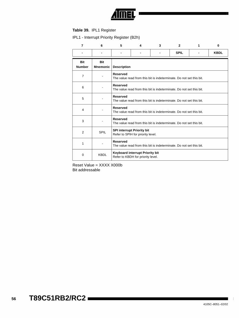
56 T89C51RB2/RC24105C–8051–02/02
Table 39. IPL1 Register
IPL1 - Interrupt Priority Register (B2h)
Reset Value = XXXX X000bBit addressable
7 6 5 4 3 2 1 0
- - - - - SPIL - KBDL
Bit
Number
Bit
Mnemonic Description
7 -ReservedThe value read from this bit is indeterminate. Do not set this bit.
6 -ReservedThe value read from this bit is indeterminate. Do not set this bit.
5 -ReservedThe value read from this bit is indeterminate. Do not set this bit.
4 -ReservedThe value read from this bit is indeterminate. Do not set this bit.
3 -ReservedThe value read from this bit is indeterminate. Do not set this bit.
2 SPILSPI interrupt Priority bitRefer to SPIH for priority level.
1 -ReservedThe value read from this bit is indeterminate. Do not set this bit.
0 KBDLKeyboard interrupt Priority bitRefer to KBDH for priority level.
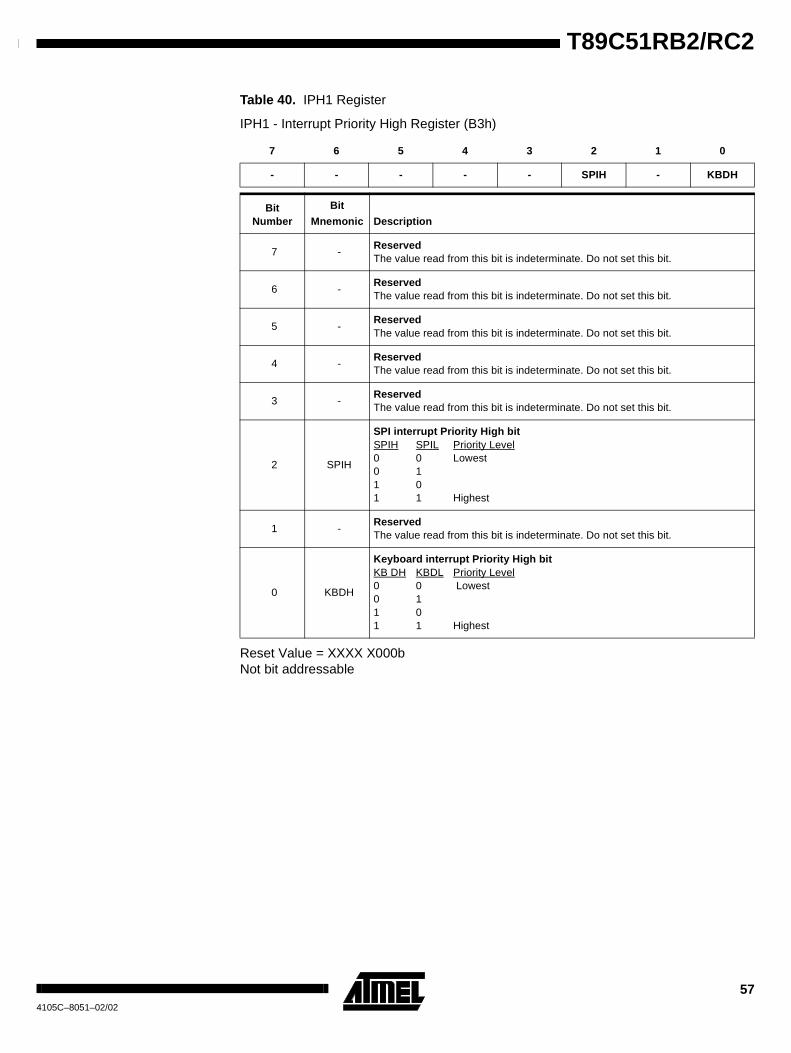
57
T89C51RB2/RC2
4105C–8051–02/02
Table 40. IPH1 Register
IPH1 - Interrupt Priority High Register (B3h)
Reset Value = XXXX X000bNot bit addressable
7 6 5 4 3 2 1 0
- - - - - SPIH - KBDH
BitNumber
Bit
Mnemonic Description
7 -ReservedThe value read from this bit is indeterminate. Do not set this bit.
6 -ReservedThe value read from this bit is indeterminate. Do not set this bit.
5 -ReservedThe value read from this bit is indeterminate. Do not set this bit.
4 -ReservedThe value read from this bit is indeterminate. Do not set this bit.
3 -ReservedThe value read from this bit is indeterminate. Do not set this bit.
2 SPIH
SPI interrupt Priority High bitSPIH SPIL Priority Level0 0 Lowest0 11 01 1 Highest
1 -ReservedThe value read from this bit is indeterminate. Do not set this bit.
0 KBDH
Keyboard interrupt Priority High bitKB DH KBDL Priority Level0 0 Lowest0 11 01 1 Highest
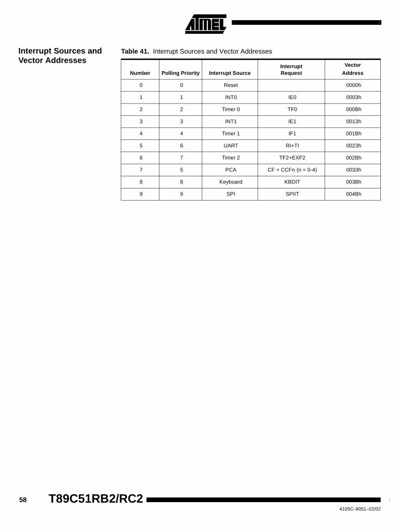
58 T89C51RB2/RC24105C–8051–02/02
Interrupt Sources andVector Addresses
Table 41. Interrupt Sources and Vector Addresses
Number Polling Priority Interrupt SourceInterruptRequest
Vector
Address
0 0 Reset 0000h
1 1 INT0 IE0 0003h
2 2 Timer 0 TF0 000Bh
3 3 INT1 IE1 0013h
4 4 Timer 1 IF1 001Bh
5 6 UART RI+TI 0023h
6 7 Timer 2 TF2+EXF2 002Bh
7 5 PCA CF + CCFn (n = 0-4) 0033h
8 8 Keyboard KBDIT 003Bh
9 9 SPI SPIIT 004Bh
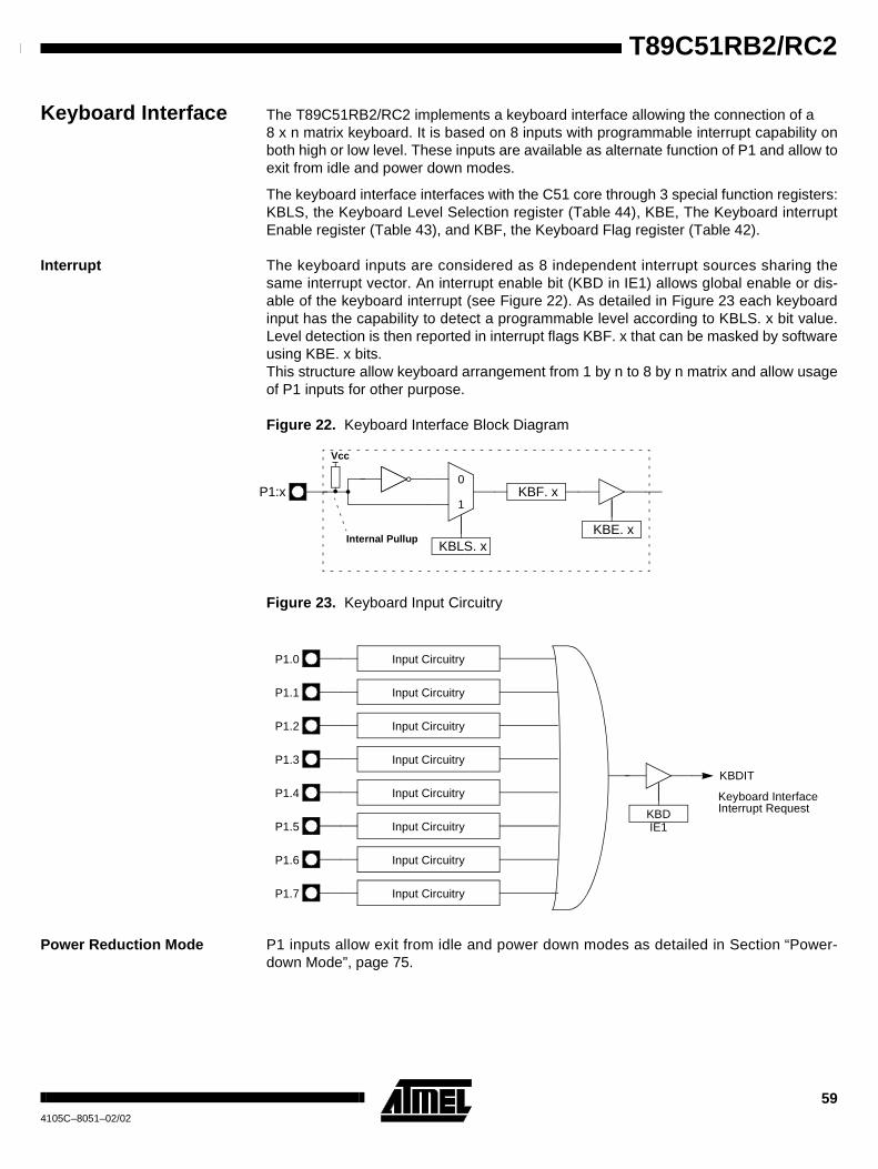
59
T89C51RB2/RC2
4105C–8051–02/02
Keyboard Interface The T89C51RB2/RC2 implements a keyboard interface allowing the connection of a8 x n matrix keyboard. It is based on 8 inputs with programmable interrupt capability onboth high or low level. These inputs are available as alternate function of P1 and allow toexit from idle and power down modes.
The keyboard interface interfaces with the C51 core through 3 special function registers:KBLS, the Keyboard Level Selection register (Table 44), KBE, The Keyboard interruptEnable register (Table 43), and KBF, the Keyboard Flag register (Table 42).
Interrupt The keyboard inputs are considered as 8 independent interrupt sources sharing thesame interrupt vector. An interrupt enable bit (KBD in IE1) allows global enable or dis-able of the keyboard interrupt (see Figure 22). As detailed in Figure 23 each keyboardinput has the capability to detect a programmable level according to KBLS. x bit value.Level detection is then reported in interrupt flags KBF. x that can be masked by softwareusing KBE. x bits.This structure allow keyboard arrangement from 1 by n to 8 by n matrix and allow usageof P1 inputs for other purpose.
Figure 22. Keyboard Interface Block Diagram
Figure 23. Keyboard Input Circuitry
Power Reduction Mode P1 inputs allow exit from idle and power down modes as detailed in Section “Power-down Mode”, page 75.
P1:x
KBE. x
KBF. x
KBLS. x
0
1
Vcc
Internal Pullup
P1.0
Keyboard InterfaceInterrupt RequestKBD
IE1
Input Circuitry
P1.1 Input Circuitry
P1.2 Input Circuitry
P1.3 Input Circuitry
P1.4 Input Circuitry
P1.5 Input Circuitry
P1.6 Input Circuitry
P1.7 Input Circuitry
KBDIT
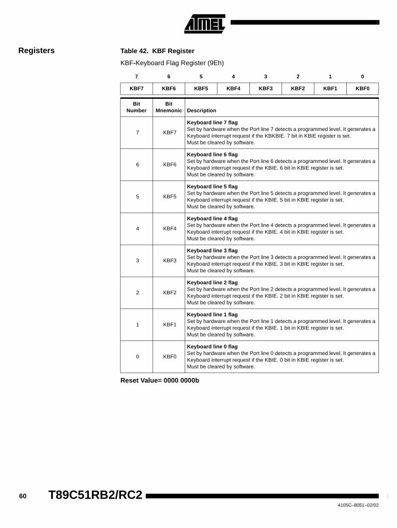
60 T89C51RB2/RC24105C–8051–02/02
Registers Table 42. KBF Register
KBF-Keyboard Flag Register (9Eh)
Reset Value= 0000 0000b
7 6 5 4 3 2 1 0
KBF7 KBF6 KBF5 KBF4 KBF3 KBF2 KBF1 KBF0
BitNumber
BitMnemonic Description
7 KBF7
Keyboard line 7 flagSet by hardware when the Port line 7 detects a programmed level. It generates aKeyboard interrupt request if the KBKBIE. 7 bit in KBIE register is set.Must be cleared by software.
6 KBF6
Keyboard line 6 flagSet by hardware when the Port line 6 detects a programmed level. It generates aKeyboard interrupt request if the KBIE. 6 bit in KBIE register is set.Must be cleared by software.
5 KBF5
Keyboard line 5 flagSet by hardware when the Port line 5 detects a programmed level. It generates aKeyboard interrupt request if the KBIE. 5 bit in KBIE register is set.Must be cleared by software.
4 KBF4
Keyboard line 4 flagSet by hardware when the Port line 4 detects a programmed level. It generates aKeyboard interrupt request if the KBIE. 4 bit in KBIE register is set.Must be cleared by software.
3 KBF3
Keyboard line 3 flagSet by hardware when the Port line 3 detects a programmed level. It generates aKeyboard interrupt request if the KBIE. 3 bit in KBIE register is set.Must be cleared by software.
2 KBF2
Keyboard line 2 flagSet by hardware when the Port line 2 detects a programmed level. It generates aKeyboard interrupt request if the KBIE. 2 bit in KBIE register is set.Must be cleared by software.
1 KBF1
Keyboard line 1 flagSet by hardware when the Port line 1 detects a programmed level. It generates aKeyboard interrupt request if the KBIE. 1 bit in KBIE register is set.Must be cleared by software.
0 KBF0
Keyboard line 0 flagSet by hardware when the Port line 0 detects a programmed level. It generates aKeyboard interrupt request if the KBIE. 0 bit in KBIE register is set.Must be cleared by software.
61
T89C51RB2/RC2
4105C–8051–02/02
Table 43. KBE Register
KBE-Keyboard Input Enable Register (9Dh)
Reset Value= 0000 0000b
7 6 5 4 3 2 1 0
KBE7 KBE6 KBE5 KBE4 KBE3 KBE2 KBE1 KBE0
BitNumber
BitMnemonic Description
7 KBE7Keyboard line 7 Enable bitCleared to enable standard I/O pin.Set to enable KBF. 7 bit in KBF register to generate an interrupt request.
6 KBE6Keyboard line 6 Enable bitCleared to enable standard I/O pin.Set to enable KBF. 6 bit in KBF register to generate an interrupt request.
5 KBE5Keyboard line 5 Enable bitCleared to enable standard I/O pin.Set to enable KBF. 5 bit in KBF register to generate an interrupt request.
4 KBE4Keyboard line 4 Enable bitCleared to enable standard I/O pin.Set to enable KBF. 4 bit in KBF register to generate an interrupt request.
3 KBE3Keyboard line 3 Enable bitCleared to enable standard I/O pin.Set to enable KBF. 3 bit in KBF register to generate an interrupt request.
2 KBE2Keyboard line 2 Enable bitCleared to enable standard I/O pin.Set to enable KBF. 2 bit in KBF register to generate an interrupt request.
1 KBE1Keyboard line 1 Enable bitCleared to enable standard I/O pin.Set to enable KBF. 1 bit in KBF register to generate an interrupt request.
0 KBE0Keyboard line 0 Enable bitCleared to enable standard I/O pin.Set to enable KBF. 0 bit in KBF register to generate an interrupt request.
62 T89C51RB2/RC24105C–8051–02/02
Table 44. KBLS Register
KBLS-Keyboard Level Selector Register (9Ch)
Reset Value= 0000 0000b
7 6 5 4 3 2 1 0
KBLS7 KBLS6 KBLS5 KBLS4 KBLS3 KBLS2 KBLS1 KBLS0
BitNumber
BitMnemonic Description
7 KBLS7Keyboard line 7 Level Selection bitCleared to enable a low level detection on Port line 7.Set to enable a high level detection on Port line 7.
6 KBLS6Keyboard line 6 Level Selection bitCleared to enable a low level detection on Port line 6.Set to enable a high level detection on Port line 6.
5 KBLS5Keyboard line 5 Level Selection bitCleared to enable a low level detection on Port line 5.Set to enable a high level detection on Port line 5.
4 KBLS4Keyboard line 4 Level Selection bitCleared to enable a low level detection on Port line 4.Set to enable a high level detection on Port line 4.
3 KBLS3Keyboard line 3 Level Selection bitCleared to enable a low level detection on Port line 3.Set to enable a high level detection on Port line 3.
2 KBLS2Keyboard line 2 Level Selection bitCleared to enable a low level detection on Port line 2.Set to enable a high level detection on Port line 2.
1 KBLS1Keyboard line 1 Level Selection bitCleared to enable a low level detection on Port line 1.Set to enable a high level detection on Port line 1.
0 KBLS0Keyboard line 0 Level Selection bitCleared to enable a low level detection on Port line 0.Set to enable a high level detection on Port line 0.
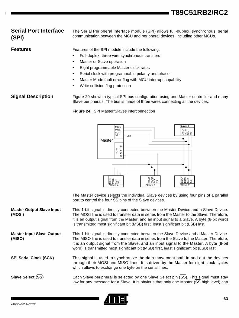
63
T89C51RB2/RC2
4105C–8051–02/02
Serial Port Interface(SPI)
The Serial Peripheral Interface module (SPI) allows full-duplex, synchronous, serialcommunication between the MCU and peripheral devices, including other MCUs.
Features Features of the SPI module include the following:
• Full-duplex, three-wire synchronous transfers
• Master or Slave operation
• Eight programmable Master clock rates
• Serial clock with programmable polarity and phase
• Master Mode fault error flag with MCU interrupt capability
• Write collision flag protection
Signal Description Figure 20 shows a typical SPI bus configuration using one Master controller and manySlave peripherals. The bus is made of three wires connecting all the devices:
Figure 24. SPI Master/Slaves interconnection
The Master device selects the individual Slave devices by using four pins of a parallelport to control the four SS pins of the Slave devices.
Master Output Slave Input(MOSI)
This 1-bit signal is directly connected between the Master Device and a Slave Device.The MOSI line is used to transfer data in series from the Master to the Slave. Therefore,it is an output signal from the Master, and an input signal to a Slave. A byte (8-bit word)is transmitted most significant bit (MSB) first, least significant bit (LSB) last.
Master Input Slave Output(MISO)
This 1-bit signal is directly connected between the Slave Device and a Master Device.The MISO line is used to transfer data in series from the Slave to the Master. Therefore,it is an output signal from the Slave, and an input signal to the Master. A byte (8-bitword) is transmitted most significant bit (MSB) first, least significant bit (LSB) last.
SPI Serial Clock (SCK) This signal is used to synchronize the data movement both in and out the devicesthrough their MOSI and MISO lines. It is driven by the Master for eight clock cycleswhich allows to exchange one byte on the serial lines.
Slave Select (SS) Each Slave peripheral is selected by one Slave Select pin (SS). This signal must staylow for any message for a Slave. It is obvious that only one Master (SS high level) can
Slave 1
MIS
OM
OS
IS
CK
SS
MISOMOSISCKSS
PO
RT
0123
Slave 3
MIS
OM
OS
IS
CK
SS
Slave 4
MIS
OM
OS
IS
CK
SS
Slave 2M
ISO
MO
SI
SC
KS
S
VDD
Master
64 T89C51RB2/RC24105C–8051–02/02
drive the network. The Master may select each Slave device by software through portpins (Figure 20). To prevent bus conflicts on the MISO line, only one slave should beselected at a time by the Master for a transmission.
In a Master configuration, the SS line can be used in conjunction with the MODF flag inthe SPI Status register (SPSTA) to prevent multiple masters from driving MOSI andSCK (See Error conditions).
A high level on the SS pin puts the MISO line of a Slave SPI in a high-impedance state.
The SS pin could be used as a general purpose if the following conditions are met:
• The device is configured as a Master and the SSDIS control bit in SPCON is set.This kind of configuration can be found when only one Master is driving the networkand there is no way that the SS pin could be pulled low. Therefore, the MODF flag inthe SPSTA will never be set(1).
• The Device is configured as a Slave with CPHA and SSDIS control bits set(2) Thiskind of configuration can happen when the system comprises one Master and oneSlave only. Therefore, the device should always be selected and there is no reasonthat the Master uses the SS pin to select the communicating Slave device.
Note: 1. Clearing SSDIS control bit does not clear MODF.
2. Special care should be taken not to set SSDIS control bit when CPHA =’0’ because inthis mode, the SS is used to start the transmission.
Baud rate In Master mode, the baud rate can be selected from a baud rate generator which is con-trolled by three bits in the SPCON register: SPR2, SPR1 and SPR0.The Master clock ischosen from one of seven clock rates resulting from the division of the internal clock by2, 4, 8, 16, 32, 64 or 128.
Table 45 gives the different clock rates selected by SPR2:SPR1:SPR0:
Table 45. SPI Master Baud Rate Selection
SPR2 SPR1 SPR0 Clock Rate Baud rate divisor (BD)
0 0 0 FCLK PERIPH /2 2
0 0 1 FCLK PERIPH /4 4
0 1 0 FCLK PERIPH / 8 8
0 1 1 FCLK PERIPH /16 16
1 0 0 FCLK PERIPH /32 32
1 0 1 FCLK PERIPH /64 64
1 1 0 FCLK PERIPH /128 128
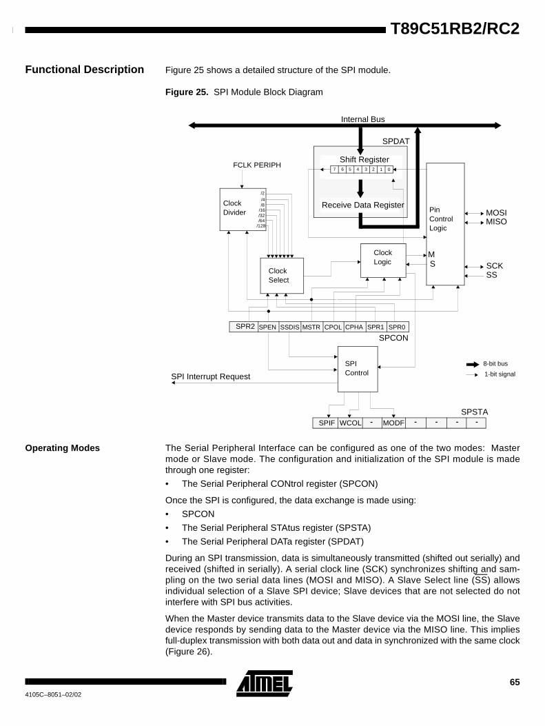
65
T89C51RB2/RC2
4105C–8051–02/02
Functional Description Figure 25 shows a detailed structure of the SPI module.
Figure 25. SPI Module Block Diagram
Operating Modes The Serial Peripheral Interface can be configured as one of the two modes: Mastermode or Slave mode. The configuration and initialization of the SPI module is madethrough one register:
• The Serial Peripheral CONtrol register (SPCON)
Once the SPI is configured, the data exchange is made using:
• SPCON
• The Serial Peripheral STAtus register (SPSTA)
• The Serial Peripheral DATa register (SPDAT)
During an SPI transmission, data is simultaneously transmitted (shifted out serially) andreceived (shifted in serially). A serial clock line (SCK) synchronizes shifting and sam-pling on the two serial data lines (MOSI and MISO). A Slave Select line (SS) allowsindividual selection of a Slave SPI device; Slave devices that are not selected do notinterfere with SPI bus activities.
When the Master device transmits data to the Slave device via the MOSI line, the Slavedevice responds by sending data to the Master device via the MISO line. This impliesfull-duplex transmission with both data out and data in synchronized with the same clock(Figure 26).
Shift Register01234567
Internal Bus
PinControlLogic
MISOMOSI
SCKMS
ClockLogic
ClockDivider
ClockSelect
/2/4
/64/128
SPI Interrupt Request
8-bit bus
1-bit signal
SS
FCLK PERIPH
/32
/8/16
Receive Data Register
SPDAT
SPIControl
SPSTA
CPHA SPR0SPR1CPOLMSTRSSDISSPENSPR2
SPCON
WCOL MODFSPIF - - - - -
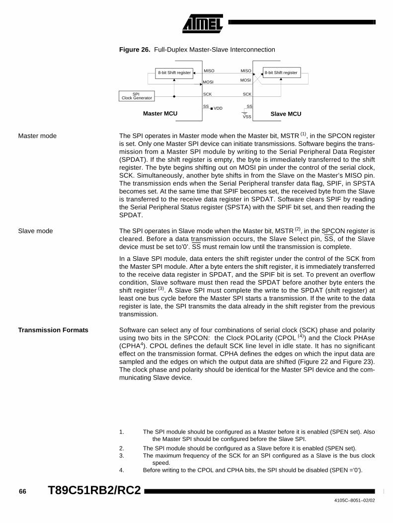
66 T89C51RB2/RC24105C–8051–02/02
Figure 26. Full-Duplex Master-Slave Interconnection
Master mode The SPI operates in Master mode when the Master bit, MSTR (1), in the SPCON registeris set. Only one Master SPI device can initiate transmissions. Software begins the trans-mission from a Master SPI module by writing to the Serial Peripheral Data Register(SPDAT). If the shift register is empty, the byte is immediately transferred to the shiftregister. The byte begins shifting out on MOSI pin under the control of the serial clock,SCK. Simultaneously, another byte shifts in from the Slave on the Master’s MISO pin.The transmission ends when the Serial Peripheral transfer data flag, SPIF, in SPSTAbecomes set. At the same time that SPIF becomes set, the received byte from the Slaveis transferred to the receive data register in SPDAT. Software clears SPIF by readingthe Serial Peripheral Status register (SPSTA) with the SPIF bit set, and then reading theSPDAT.
Slave mode The SPI operates in Slave mode when the Master bit, MSTR (2), in the SPCON register iscleared. Before a data transmission occurs, the Slave Select pin, SS, of the Slavedevice must be set to’0’. SS must remain low until the transmission is complete.
In a Slave SPI module, data enters the shift register under the control of the SCK fromthe Master SPI module. After a byte enters the shift register, it is immediately transferredto the receive data register in SPDAT, and the SPIF bit is set. To prevent an overflowcondition, Slave software must then read the SPDAT before another byte enters theshift register (3). A Slave SPI must complete the write to the SPDAT (shift register) atleast one bus cycle before the Master SPI starts a transmission. If the write to the dataregister is late, the SPI transmits the data already in the shift register from the previoustransmission.
Transmission Formats Software can select any of four combinations of serial clock (SCK) phase and polarityusing two bits in the SPCON: the Clock POLarity (CPOL (4)) and the Clock PHAse(CPHA4). CPOL defines the default SCK line level in idle state. It has no significanteffect on the transmission format. CPHA defines the edges on which the input data aresampled and the edges on which the output data are shifted (Figure 22 and Figure 23).The clock phase and polarity should be identical for the Master SPI device and the com-municating Slave device.
8-bit Shift register
SPIClock Generator
Master MCU
8-bit Shift registerMISOMISO
MOSI MOSI
SCK SCK
VSS
VDD SSSS
Slave MCU
1. The SPI module should be configured as a Master before it is enabled (SPEN set). Alsothe Master SPI should be configured before the Slave SPI.
2. The SPI module should be configured as a Slave before it is enabled (SPEN set).3. The maximum frequency of the SCK for an SPI configured as a Slave is the bus clock
speed.4. Before writing to the CPOL and CPHA bits, the SPI should be disabled (SPEN =’0’).
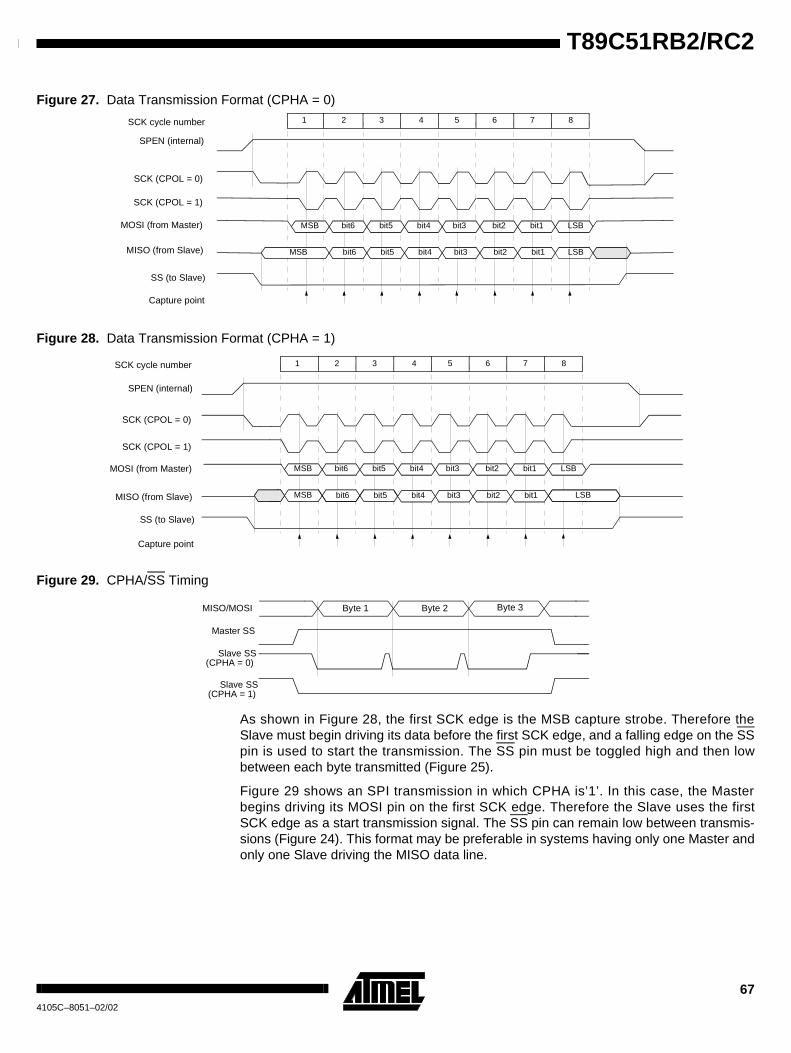
67
T89C51RB2/RC2
4105C–8051–02/02
Figure 27. Data Transmission Format (CPHA = 0)
Figure 28. Data Transmission Format (CPHA = 1)
Figure 29. CPHA/SS Timing
As shown in Figure 28, the first SCK edge is the MSB capture strobe. Therefore theSlave must begin driving its data before the first SCK edge, and a falling edge on the SSpin is used to start the transmission. The SS pin must be toggled high and then lowbetween each byte transmitted (Figure 25).
Figure 29 shows an SPI transmission in which CPHA is’1’. In this case, the Masterbegins driving its MOSI pin on the first SCK edge. Therefore the Slave uses the firstSCK edge as a start transmission signal. The SS pin can remain low between transmis-sions (Figure 24). This format may be preferable in systems having only one Master andonly one Slave driving the MISO data line.
MSB bit6 bit5 bit4 bit3 bit2 bit1 LSB
bit6 bit5 bit4 bit3 bit2 bit1MSB LSB
1 32 4 5 6 7 8
Capture point
SS (to Slave)
MISO (from Slave)
MOSI (from Master)
SCK (CPOL = 1)
SCK (CPOL = 0)
SPEN (internal)
SCK cycle number
MSB bit6 bit5 bit4 bit3 bit2 bit1 LSB
bit6 bit5 bit4 bit3 bit2 bit1MSB LSB
1 32 4 5 6 7 8
Capture point
SS (to Slave)
MISO (from Slave)
MOSI (from Master)
SCK (CPOL = 1)
SCK (CPOL = 0)
SPEN (internal)
SCK cycle number
Byte 1 Byte 2 Byte 3MISO/MOSI
Master SS
Slave SS(CPHA = 1)
Slave SS(CPHA = 0)
68 T89C51RB2/RC24105C–8051–02/02
Error conditions The following flags in the SPSTA signal SPI error conditions:
Mode Fault (MODF) Mode Fault error in Master mode SPI indicates that the level on the Slave Select (SS)pin is inconsistent with the actual mode of the device. MODF is set to warn that theremay have a multi-master conflict for system control. In this case, the SPI system isaffected in the following ways:
• An SPI receiver/error CPU interrupt request is generated,
• The SPEN bit in SPCON is cleared. This disable the SPI,
• The MSTR bit in SPCON is cleared
When SS DISable (SSDIS) bit in the SPCON register is cleared, the MODF flag is setwhen the SS signal becomes’0’.
However, as stated before, for a system with one Master, if the SS pin of the Masterdevice is pulled low, there is no way that another Master attempt to drive the network. Inthis case, to prevent the MODF flag from being set, software can set the SSDIS bit in theSPCON register and therefore making the SS pin as a general purpose I/O pin.
Clearing the MODF bit is accomplished by a read of SPSTA register with MODF bit set,followed by a write to the SPCON register. SPEN Control bit may be restored to its orig-inal set state after the MODF bit has been cleared.
Write Collision (WCOL) A Write Collision (WCOL) flag in the SPSTA is set when a write to the SPDAT register isdone during a transmit sequence.
WCOL does not cause an interruption, and the transfer continues uninterrupted.
Clearing the WCOL bit is done through a software sequence of an access to SPSTAand an access to SPDAT.
Overrun Condition An overrun condition occurs when the Master device tries to send several data bytesand the Slave devise has not cleared the SPIF bit issuing from the previous data bytetransmitted. In this case, the receiver buffer contains the byte sent after the SPIF bit waslast cleared. A read of the SPDAT returns this byte. All others bytes are lost.
This condition is not detected by the SPI peripheral.
Interrupts Two SPI status flags can generate a CPU interrupt requests:
Table 46. SPI Interrupts
Serial Peripheral data transfer flag, SPIF: This bit is set by hardware when a transferhas been completed. SPIF bit generates transmitter CPU interrupt requests.
Mode Fault flag, MODF: This bit becomes set to indicate that the level on the SS isinconsistent with the mode of the SPI. MODF with SSDIS reset, generates receiver/errorCPU interrupt requests.
Figure 30 gives a logical view of the above statements.
Flag Request
SPIF (SP data transfer) SPI Transmitter Interrupt request
MODF (Mode Fault) SPI Receiver/Error Interrupt Request (if SSDIS =’0’)
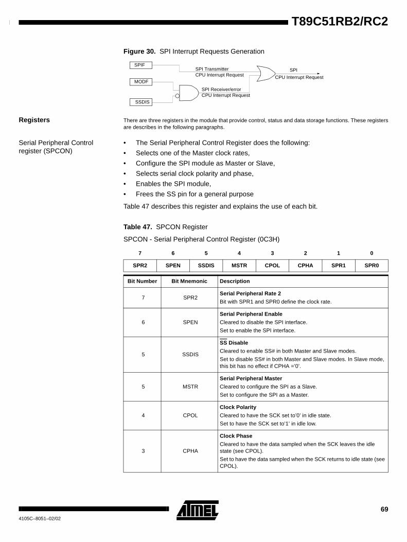
69
T89C51RB2/RC2
4105C–8051–02/02
Figure 30. SPI Interrupt Requests Generation
Registers There are three registers in the module that provide control, status and data storage functions. These registersare describes in the following paragraphs.
Serial Peripheral Controlregister (SPCON)
• The Serial Peripheral Control Register does the following:
• Selects one of the Master clock rates,
• Configure the SPI module as Master or Slave,
• Selects serial clock polarity and phase,
• Enables the SPI module,
• Frees the SS pin for a general purpose
Table 47 describes this register and explains the use of each bit.
Table 47. SPCON Register
SPCON - Serial Peripheral Control Register (0C3H)
SSDIS
MODF
CPU Interrupt RequestSPI Receiver/error
CPU Interrupt RequestSPI Transmitter SPI
CPU Interrupt Request
SPIF
7 6 5 4 3 2 1 0
SPR2 SPEN SSDIS MSTR CPOL CPHA SPR1 SPR0
Bit Number Bit Mnemonic Description
7 SPR2Serial Peripheral Rate 2
Bit with SPR1 and SPR0 define the clock rate.
6 SPEN
Serial Peripheral Enable
Cleared to disable the SPI interface.
Set to enable the SPI interface.
5 SSDIS
SS Disable
Cleared to enable SS# in both Master and Slave modes.
Set to disable SS# in both Master and Slave modes. In Slave mode,this bit has no effect if CPHA =’0’.
5 MSTR
Serial Peripheral Master
Cleared to configure the SPI as a Slave.
Set to configure the SPI as a Master.
4 CPOL
Clock Polarity
Cleared to have the SCK set to’0’ in idle state.
Set to have the SCK set to’1’ in idle low.
3 CPHA
Clock Phase
Cleared to have the data sampled when the SCK leaves the idlestate (see CPOL).
Set to have the data sampled when the SCK returns to idle state (seeCPOL).
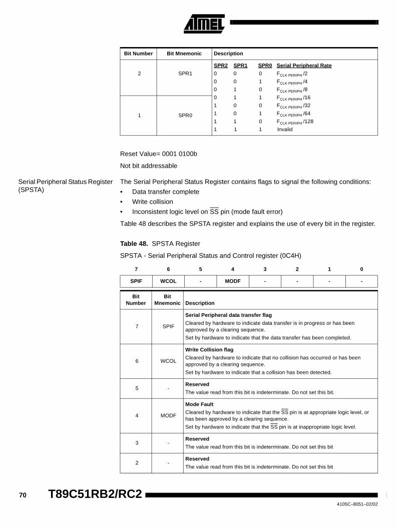
70 T89C51RB2/RC24105C–8051–02/02
Reset Value= 0001 0100b
Not bit addressable
Serial Peripheral Status Register(SPSTA)
The Serial Peripheral Status Register contains flags to signal the following conditions:
• Data transfer complete
• Write collision
• Inconsistent logic level on SS pin (mode fault error)
Table 48 describes the SPSTA register and explains the use of every bit in the register.
Table 48. SPSTA Register
SPSTA - Serial Peripheral Status and Control register (0C4H)
2 SPR1
SPR2 SPR1 SPR0 Serial Peripheral Rate
0 0 0 FCLK PERIPH /2
0 0 1 FCLK PERIPH /4
0 1 0 FCLK PERIPH /8
0 1 1 FCLK PERIPH /16
1 0 0 FCLK PERIPH /32
1 0 1 FCLK PERIPH /64
1 1 0 FCLK PERIPH /128
1 1 1 Invalid
1 SPR0
Bit Number Bit Mnemonic Description
7 6 5 4 3 2 1 0
SPIF WCOL - MODF - - - -
BitNumber
BitMnemonic Description
7 SPIF
Serial Peripheral data transfer flag
Cleared by hardware to indicate data transfer is in progress or has beenapproved by a clearing sequence.
Set by hardware to indicate that the data transfer has been completed.
6 WCOL
Write Collision flag
Cleared by hardware to indicate that no collision has occurred or has beenapproved by a clearing sequence.
Set by hardware to indicate that a collision has been detected.
5 -Reserved
The value read from this bit is indeterminate. Do not set this bit.
4 MODF
Mode Fault
Cleared by hardware to indicate that the SS pin is at appropriate logic level, orhas been approved by a clearing sequence.
Set by hardware to indicate that the SS pin is at inappropriate logic level.
3 -Reserved
The value read from this bit is indeterminate. Do not set this bit
2 -Reserved
The value read from this bit is indeterminate. Do not set this bit
71
T89C51RB2/RC2
4105C–8051–02/02
Reset Value= 00X0 XXXXb
Not Bit addressable
Serial Peripheral DATa register(SPDAT)
The Serial Peripheral Data Register (Table 49) is a read/write buffer for the receive dataregister. A write to SPDAT places data directly into the shift register. No transmit buffer isavailable in this model.
A Read of the SPDAT returns the value located in the receive buffer and not the contentof the shift register.
Table 49. SPDAT Register
SPDAT - Serial Peripheral Data Register (0C5H)
Reset Value= Indeterminate
R7:R0: Receive data bits
SPCON, SPSTA and SPDAT registers may be read and written at any time while thereis no on-going exchange. However, special care should be taken when writing to themwhile a transmission is on-going:
• Do not change SPR2, SPR1 and SPR0
• Do not change CPHA and CPOL
• Do not change MSTR
• Clearing SPEN would immediately disable the peripheral
• Writing to the SPDAT will cause an overflow
1 -Reserved
The value read from this bit is indeterminate. Do not set this bit.
0 -Reserved
The value read from this bit is indeterminate. Do not set this bit.
BitNumber
BitMnemonic Description
7 6 5 4 3 2 1 0
R7 R6 R5 R4 R3 R2 R1 R0
72 T89C51RB2/RC24105C–8051–02/02
Hardware WatchdogTimer
The WDT is intended as a recovery method in situations where the CPU may be sub-jected to software upset. The WDT consists of a 14-bit counter and the WatchDog TimerReSeT (WDTRST) SFR. The WDT is by default disabled from exiting reset. To enablethe WDT, user must write 01EH and 0E1H in sequence to the WDTRST, SFR location0A6H. When WDT is enabled, it will increment every machine cycle while the oscillatoris running and there is no way to disable the WDT except through reset (either hardwarereset or WDT overflow reset). When WDT overflows, it will drive an output RESET HIGHpulse at the RST-pin.
Using the WDT To enable the WDT, user must write 01EH and 0E1H in sequence to the WDTRST, SFRlocation 0A6H. When WDT is enabled, the user needs to service it by writing to 01EHand 0E1H to WDTRST to avoid WDT overflow. The 14-bit counter overflows when itreaches 16383 (3FFFH) and this will reset the device. When WDT is enabled, it willincrement every machine cycle while the oscillator is running. This means the user mustreset the WDT at least every 16383 machine cycle. To reset the WDT the user mustwrite 01EH and 0E1H to WDTRST. WDTRST is a write only register. The WDT countercannot be read or written. When WDT overflows, it will generate an output RESET pulseat the RST-pin. The RESET pulse duration is 96 x TCLK PERIPH, where TCLK PERIPH= 1/FCLK
PERIPH. To make the best use of the WDT, it should be serviced in those sections of codethat will periodically be executed within the time required to prevent a WDT reset.
To have a more powerful WDT, a 27 counter has been added to extend the Time-outcapability, ranking from 16ms to 2s @ FOSCA = 12MHz. To manage this feature, refer toWDTPRG register description, Table 50.
Table 50. WDTRST Register
WDTRST - Watchdog Reset Register (0A6h)
Reset Value = XXXX XXXXb
Write only, this SFR is used to reset/enable the WDT by writing 01EH then 0E1H insequence.
7 6 5 4 3 2 1 0
- - - - - - - -
73
T89C51RB2/RC2
4105C–8051–02/02
Table 51. WDTPRG Register
WDTPRG - Watchdog Timer Out Register (0A7h)
Reset value XXXX X000
WDT During Power Downand Idle
In Power Down mode the oscillator stops, which means the WDT also stops. While inPower Down mode the user does not need to service the WDT. There are 2 methods ofexiting Power Down mode: by a hardware reset or via a level activated external inter-rupt which is enabled prior to entering Power Down mode. When Power Down is exitedwith hardware reset, servicing the WDT should occur as it normally should whenever theT89C51RB2/RC2 is reset. Exiting Power Down with an interrupt is significantly different.The interrupt is held low long enough for the oscillator to stabilize. When the interrupt isbrought high, the interrupt is serviced. To prevent the WDT from resetting the devicewhile the interrupt pin is held low, the WDT is not started until the interrupt is pulled high.It is suggested that the WDT be reset during the interrupt service routine.
To ensure that the WDT does not overflow within a few states of exiting of powerdown, itis better to reset the WDT just before entering powerdown.
In the Idle mode, the oscillator continues to run. To prevent the WDT from resetting theT89C51RB2/RC2 while in Idle mode, the user should always set up a timer that will peri-odically exit Idle, service the WDT, and re-enter Idle mode.
7 6 5 4 3 2 1 0
- - - - - S2 S1 S0
Bit
Number
Bit
Mnemonic Description
7 -
ReservedThe value read from this bit is undetermined. Do not try to set this bit.
6 -
5 -
4 -
3 -
2 S2 WDT Time-out select bit 2
1 S1 WDT Time-out select bit 1
0 S0 WDT Time-out select bit 0
S2 S1 S0 Selected Time-out0 0 0 (214 - 1) machine cycles, 16. 3 ms @ FOSCA =12 MHz0 0 1 (215 - 1) machine cycles, 32.7 ms @ FOSCA=12 MHz0 1 0 (216 - 1) machine cycles, 65. 5 ms @ FOSCA=12 MHz0 1 1 (217 - 1) machine cycles, 131 ms @ FOSCA=12 MHz1 0 0 (218 - 1) machine cycles, 262 ms @ FOSCA=12 MHz1 0 1 (219 - 1) machine cycles, 542 ms @ FOSCA=12 MHz1 1 0 (220 - 1) machine cycles, 1.05 s @ FOSCA=12 MHz1 1 1 (221 - 1) machine cycles, 2.09 s @ FOSCA=12 MHz
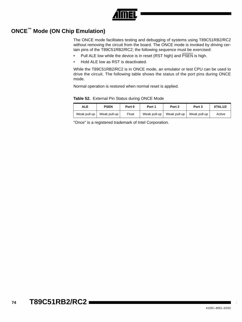
74 T89C51RB2/RC24105C–8051–02/02
ONCE™ Mode (ON Chip Emulation)The ONCE mode facilitates testing and debugging of systems using T89C51RB2/RC2without removing the circuit from the board. The ONCE mode is invoked by driving cer-tain pins of the T89C51RB2/RC2; the following sequence must be exercised:
• Pull ALE low while the device is in reset (RST high) and PSEN is high.
• Hold ALE low as RST is deactivated.
While the T89C51RB2/RC2 is in ONCE mode, an emulator or test CPU can be used todrive the circuit. The following table shows the status of the port pins during ONCEmode.
Normal operation is restored when normal reset is applied.
Table 52. External Pin Status during ONCE Mode
"Once" is a registered trademark of Intel Corporation.
ALE PSEN Port 0 Port 1 Port 2 Port 3 XTAL1/2
Weak pull-up Weak pull-up Float Weak pull-up Weak pull-up Weak pull-up Active
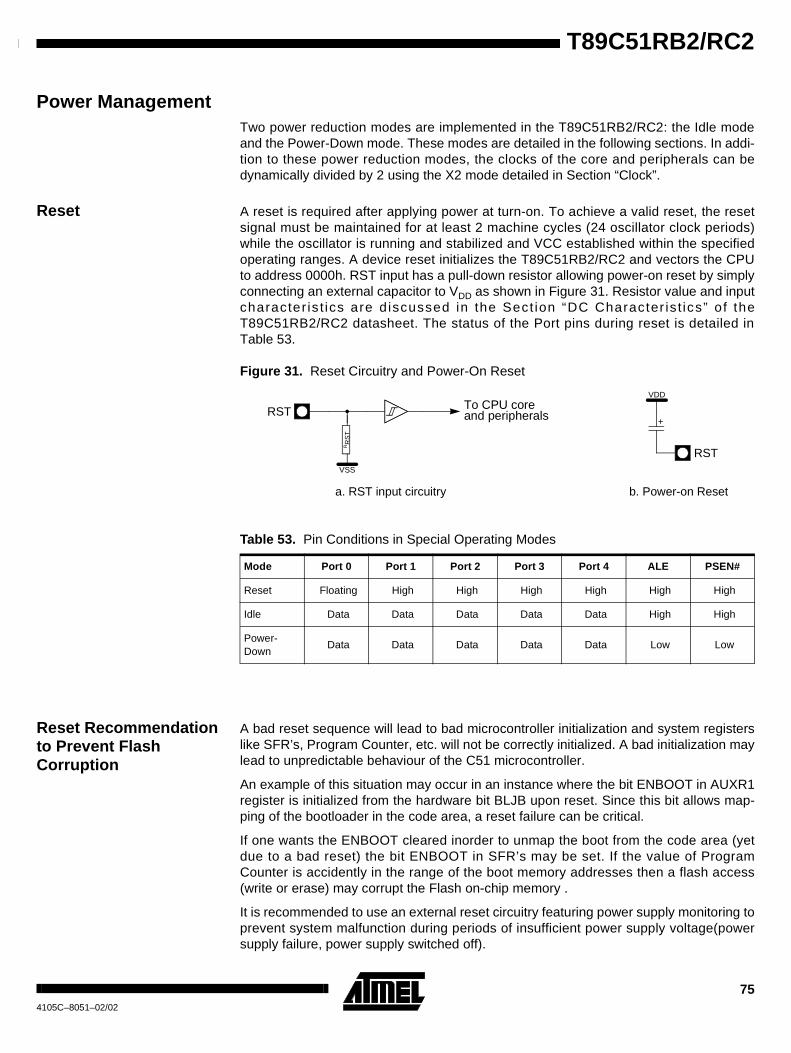
75
T89C51RB2/RC2
4105C–8051–02/02
Power ManagementTwo power reduction modes are implemented in the T89C51RB2/RC2: the Idle modeand the Power-Down mode. These modes are detailed in the following sections. In addi-tion to these power reduction modes, the clocks of the core and peripherals can bedynamically divided by 2 using the X2 mode detailed in Section “Clock”.
Reset A reset is required after applying power at turn-on. To achieve a valid reset, the resetsignal must be maintained for at least 2 machine cycles (24 oscillator clock periods)while the oscillator is running and stabilized and VCC established within the specifiedoperating ranges. A device reset initializes the T89C51RB2/RC2 and vectors the CPUto address 0000h. RST input has a pull-down resistor allowing power-on reset by simplyconnecting an external capacitor to VDD as shown in Figure 31. Resistor value and inputcharacter is t ics are discussed in the Sect ion “DC Character is t ics” of theT89C51RB2/RC2 datasheet. The status of the Port pins during reset is detailed inTable 53.
Figure 31. Reset Circuitry and Power-On Reset
Table 53. Pin Conditions in Special Operating Modes
Reset Recommendationto Prevent FlashCorruption
A bad reset sequence will lead to bad microcontroller initialization and system registerslike SFR’s, Program Counter, etc. will not be correctly initialized. A bad initialization maylead to unpredictable behaviour of the C51 microcontroller.
An example of this situation may occur in an instance where the bit ENBOOT in AUXR1register is initialized from the hardware bit BLJB upon reset. Since this bit allows map-ping of the bootloader in the code area, a reset failure can be critical.
If one wants the ENBOOT cleared inorder to unmap the boot from the code area (yetdue to a bad reset) the bit ENBOOT in SFR’s may be set. If the value of ProgramCounter is accidently in the range of the boot memory addresses then a flash access(write or erase) may corrupt the Flash on-chip memory .
It is recommended to use an external reset circuitry featuring power supply monitoring toprevent system malfunction during periods of insufficient power supply voltage(powersupply failure, power supply switched off).
Mode Port 0 Port 1 Port 2 Port 3 Port 4 ALE PSEN#
Reset Floating High High High High High High
Idle Data Data Data Data Data High High
Power-Down
Data Data Data Data Data Low Low
RST
RR
ST
VSS
To CPU coreand peripherals
RST
VDD
+
b. Power-on Reseta. RST input circuitry

76 T89C51RB2/RC24105C–8051–02/02
Idle Mode An instruction that sets PCON. 0 indicates that it is the last instruction to be executedbefore going into Idle mode. In Idle mode, the internal clock signal is gated off to theCPU, but not to the interrupt, Timer, and Serial Port functions. The CPU status is pre-served in its entirety: the Stack Pointer, Program Counter, Program Status Word,Accumulator and all other registers maintain their data during idle. The port pins hold thelogical states they had at the time Idle was activated. ALE and PSEN hold at logic highlevel.
There are two ways to terminate the Idle mode. Activation of any enabled interrupt willcause PCON. 0 to be cleared by hardware, terminating the Idle mode. The interrupt willbe serviced, and following RETI the next instruction to be executed will be the one fol-lowing the instruction that put the device into idle.
The flag bits GF0 and GF1 can be used to give an indication if an interrupt occurred dur-ing normal operation or during idle. For example, an instruction that activates idle canalso set one or both flag bits. When idle is terminated by an interrupt, the interrupt ser-vice routine can examine the flag bits.
The other way of terminating the Idle mode is with a hardware reset. Since the clockoscillator is still running, the hardware reset needs to be held active for only twomachine cycles (24 oscillator periods) to complete the reset.
Power-down Mode To save maximum power, a power-down mode can be invoked by software (refer toTable 5, PCON register).
In power-down mode, the oscillator is stopped and the instruction that invoked power-down mode is the last instruction executed. The internal RAM and SFRs retain theirvalue until the power-down mode is terminated. VCC can be lowered to save furtherpower. Either a hardware reset or an external interrupt can cause an exit from power-down. To properly terminate power-down, the reset or external interrupt should not beexecuted before VCC is restored to its normal operating level and must be held activelong enough for the oscillator to restart and stabilize.
Only external interrupts INT0, INT1 and Keyboard Interrupts are useful to exit frompower-down. For that, interrupt must be enabled and configured as level or edge sensi-tive interrupt input. When Keyboard Interrupt occurs after a power down mode, 1024clocks are necessary to exit to power down mode and enter in operating mode.
Holding the pin low restarts the oscillator but bringing the pin high completes the exit asdetailed in Figure 32. When both interrupts are enabled, the oscillator restarts as soonas one of the two inputs is held low and power down exit will be completed when the firstinput will be released. In this case the higher priority interrupt service routine is exe-cuted. Once the interrupt is serviced, the next instruction to be executed after RETI willbe the one following the instruction that put T89C51RB2/RC2 into power-down mode.
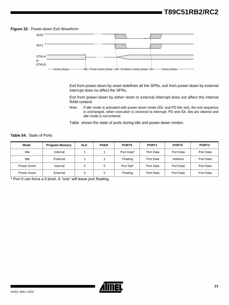
77
T89C51RB2/RC2
4105C–8051–02/02
Figure 32. Power-down Exit Waveform
Exit from power-down by reset redefines all the SFRs, exit from power-down by externalinterrupt does no affect the SFRs.
Exit from power-down by either reset or external interrupt does not affect the internalRAM content.Note: If idle mode is activated with power-down mode (IDL and PD bits set), the exit sequence
is unchanged, when execution is vectored to interrupt, PD and IDL bits are cleared andidle mode is not entered.
Table shows the state of ports during idle and power-down modes.
* Port 0 can force a 0 level. A "one" will leave port floating.
INT1
INT0
XTALA
Power-down phase Oscillator restart phase Active phaseActive phase
orXTALB
Table 54. State of Ports
Mode Program Memory ALE PSEN PORT0 PORT1 PORT2 PORT3
Idle Internal 1 1 Port Data* Port Data Port Data Port Data
Idle External 1 1 Floating Port Data Address Port Data
Power Down Internal 0 0 Port Dat* Port Data Port Data Port Data
Power Down External 0 0 Floating Port Data Port Data Port Data
77
T89C51RB2/RC2
4105C–8051–02/02
Power-off Flag The power-off flag allows the user to distinguish between a “cold start” reset and a“warm start” reset.
A cold start reset is the one induced by VCC switch-on. A warm start reset occurs whileVCC is still applied to the device and could be generated for example by an exit frompower-down.
The power-off flag (POF) is located in PCON register (Table 54). POF is set by hard-ware when VCC rises from 0 to its nominal voltage. The POF can be set or cleared bysoftware allowing the user to determine the type of reset.
Table 54. PCON Register
PCON - Power Control Register (87h)
Reset Value = 00X1 0000bNot bit addressable
7 6 5 4 3 2 1 0
SMOD1 SMOD0 - POF GF1 GF0 PD IDL
Bit
Number
Bit
Mnemonic Description
7 SMOD1Serial port Mode bit 1Set to select double baud rate in mode 1, 2 or 3.
6 SMOD0Serial port Mode bit 0Cleared to select SM0 bit in SCON register.Set to select FE bit in SCON register.
5 -ReservedThe value read from this bit is indeterminate. Do not set this bit.
4 POF
Power-Off FlagCleared to recognize next reset type.Set by hardware when VCC rises from 0 to its nominal voltage. Can also be set bysoftware.
3 GF1General purpose FlagCleared by user for general purpose usage.Set by user for general purpose usage.
2 GF0General purpose FlagCleared by user for general purpose usage.Set by user for general purpose usage.
1 PDPower-Down mode bitCleared by hardware when reset occurs.Set to enter power-down mode.
0 IDLIdle mode bitCleared by hardware when interrupt or reset occurs.Set to enter idle mode.
78 T89C51RB2/RC24105C–8051–02/02
Reduced EMI Mode The ALE signal is used to demultiplex address and data buses on port 0 when used withexternal program or data memory. Nevertheless, during internal code execution, ALEsignal is still generated. In order to reduce EMI, ALE signal can be disabled by settingAO bit.
The AO bit is located in AUXR register at bit location 0.As soon as AO is set, ALE is nolonger output but remains active during MOVX and MOVC instructions and externalfetches. During ALE disabling, ALE pin is weakly pulled high.
Table 55. AUXR Register
AUXR - Auxiliary Register (8Eh)
7 6 5 4 3 2 1 0
- - M0 - XRS1 XRS0 EXTRAM AO
Bit
Number
Bit
Mnemonic Description
7 -Reserved
The value read from this bit is indeterminate. Do not set this bit
6 -Reserved
The value read from this bit is indeterminate. Do not set this bit
5 M0
Pulse length
Cleared to stretch MOVX control: the RD/ and the WR/ pulse length is 6 clockperiods (default).
Set to stretch MOVX control: the RD/ and the WR/ pulse length is 30 clockperiods.
4 -Reserved
The value read from this bit is indeterminate. Do not set this bit
3 XRS1 XRAM Size
XRS1 XRS0 XRAM size0 0 256 bytes (default)
0 1 512 bytes
1 0 768 bytes
1 1 1024 bytes
2 XRS0
1 EXTRAM
EXTRAM bitCleared to access internal XRAM using movx @ Ri/ @ DPTR.
Set to access external memory.
Programmed by hardware after Power-up regarding Hardware Security Byte(HSB), default setting, XRAM selected.
0 AO
ALE Output bitCleared, ALE is emitted at a constant rate of 1/6 the oscillator frequency (or 1/3 ifX2 mode is used). (default) Set, ALE is active only during a MOVX or MOVCinstruction is used.
79
T89C51RB2/RC2
4105C–8051–02/02
Electrical Characteristics
Absolute Maximum Ratings(*)
Note: 1. This value is based on the maximum allowable die temperature and the thermal resistance of the package.
Operating Temperature Range ...... 0°C to 70°C (Commercial)
................................................... -40°C to 85°C (Industrial)
Note: *Stresses at or above those listed under “Absolute Max-imum Ratings” may cause permanent damage to thedevice. This is a stress rating only and functional opera-tion of the device at these or any other conditionsabove those indicated in the operational sections of thisspecification is not implied. Exposure to absolute maxi-mum rating conditions may affect device reliability.
Storage Temperature ................................... -65°C to +150°C
Voltage on VCC to VSS...................................-0.5V to + 6. 5V
Voltage on Any Pin to VSS...................... -0.5V to VCC + 0.5V
Power Dissipation........................................................... 1 W(1)
80 T89C51RB2/RC24105C–8051–02/02
DC Parameters for Standard VoltageTA = 0°C to +70°C; VSS = 0V; VCC = 5V ± 10%; F = 0 to 40 MHz.TA = -40°C to +85°C; VSS = 0V; VCC = 5V ± 10%; F = 0 to 40 MHz.
Note: 3. Power Down ICC is measured with all output pins disconnected; EA = VSS, PORT 0 = VCC; XTAL2 NC. ; RST = VSS
4. Capacitance loading on Ports 0 and 2 may cause spurious noise pulses to be superimposed on the VOLs of ALE and Ports 1and 3.The noise is due to external bus capacitance discharging into the Port 0 and Port 2 pins when these pins make 1 to 0transitions during bus operation. In the worst cases (capacitive loading 100pF), the noise pulse on the ALE line may exceed0.45V with maxi VOL peak 0.6V. A Schmitt Trigger use is not necessary.
5. Typicals are based on a limited number of samples and are not guaranteed. The values listed are at room temperature and 5V.6. Under steady state (non-transient) conditions, IOL must be externally limited as follows:
Maximum IOL per port pin: 10 mAMaximum IOL per 8-bit port:Port 0: 26 mA
Table 56. DC Parameters in Standard Voltage
Symbol Parameter Min Typ Max Unit Test Conditions
VIL Input Low Voltage -0.5 0.2 VCC - 0.1 V
VIH Input High Voltage except RST, XTAL1, 0.2 VCC + 0.9 VCC + 0.5 V
VIH1 Input High Voltage RST, XTAL1 0.7 VCC VCC + 0.5 V
VOL Output Low Voltage, ports 1, 2, 3, 4 and 5 (6)
0.3
0.45
1.0
V
V
V
IOL = 100 µA(4)
IOL = 1.6 mA(4)
IOL = 3.5 mA(4)
VOL1 Output Low Voltage, port 0, ALE, PSEN (6)
0.3
0.45
1.0
V
V
V
IOL = 200 µA(4)
IOL = 3.2 mA(4)
IOL = 7. 0 mA(4)
VOH Output High Voltage, ports 1, 2, 3, 4 and 5
VCC - 0.3
VCC - 0.7
VCC - 1.5
V
V
V
IOH = -10 µA
IOH = -30 µA
IOH = -60 µA
VCC = 5V ± 10%
VOH1 Output High Voltage, port 0, ALE, PSEN
VCC - 0.3
VCC - 0.7
VCC - 1.5
V
V
V
IOH = -200 µA
IOH = -3.2 mA
IOH = -7. 0 mA
VCC = 5V ± 10%
RRST RST Pulldown Resistor 50 90 (5) 200 kΩ
IIL Logical 0 Input Current ports 1, 2, 3, 4 and 5 -50 µA Vin = 0.45 V
ILI Input Leakage Current ±10 µA 0.45V < Vin < VCC
ITLLogical 1 to 0 Transition Current, ports 1, 2, 3, 4and 5
-650 µA Vin = 2.0 V
CIO Capacitance of I/O Buffer 10 pFFc = 1 MHzTA = 25°C
IPD Power Down Current 100 150 µA 4. 5V < VCC < 5. 5 V(3)
ICCIDLE Power Supply Current on idle mode (7) TBD mA
ICC Power Supply Current on normal mode (7) 0.4 Freq (Mhz)+ 3 mA
mA
ICCOP1 Power Supply Current Flash programming (7) 0.4 Freq (Mhz)+ 20 mA
mA
81
T89C51RB2/RC2
4105C–8051–02/02
Ports 1, 2 and 3: 15 mAMaximum total IOL for all output pins: 71 mAIf IOL exceeds the test condition, VOL may exceed the related specification. Pins are not guaranteed to sink current greater thanthe listed test conditions.
7. For other values, please contact your sales office.
DC Parameters for Low VoltageTA = 0°C to +70°C; VSS = 0V; VCC = 2.7V to 3.3V; F = 0 to 20 MHz.TA = -40°C to +85°C; VSS = 0V; VCC = 2.7V to 3.3V; F = 0 to 20 MHz.
Note: 1. Operating ICC is measured with all output pins disconnected; XTALA1 driven with TCLCH, TCHCL = 5 ns (see Figure 35.), VIL =VSS + 0.5 V,VIH = VCC - 0.5V; XTAL2 N. C. ; EA = RST = Port 0 = VCC. ICC would be slightly higher if a crystal oscillator used.
2. Idle ICC is measured with all output pins disconnected; XTAL1 driven with TCLCH, TCHCL = 5 ns, VIL = VSS + 0.5 V, VIH = VCC -0.5V; XTAL2 N. C; Port 0 = VCC; EA = RST = VSS (see Figure 32).
3. Power Down ICC is measured with all output pins disconnected; EA = VSS, PORT 0 = VCC; XTAL2 NC. ; RST = VSS4. Capacitance loading on Ports 0 and 2 may cause spurious noise pulses to be superimposed on the VOLs of ALE and Ports 1
and 3.The noise is due to external bus capacitance discharging into the Port 0 and Port 2 pins when these pins make 1 to 0transitions during bus operation. In the worst cases (capacitive loading 100pF), the noise pulse on the ALE line may exceed0.45V with maxi VOL peak 0.6V. A Schmitt Trigger use is not necessary.
5. Typicals are based on a limited number of samples and are not guaranteed. The values listed are at room temperature and5V.
6. Under steady state (non-transient) conditions, IOL must be externally limited as follows:Maximum IOL per port pin: 10 mAMaximum IOL per 8-bit port:Port 0: 26 mAPorts 1, 2 and 3: 15 mAMaximum total IOL for all output pins: 71 mAIf IOL exceeds the test condition, VOL may exceed the related specification. Pins are not guaranteed to sink current greaterthan the listed test conditions.
Table 57. DC Parameters for Low Voltage
Symbol Parameter Min Typ Max Unit Test Conditions
VIL Input Low Voltage -0.5 0.2 VCC - 0.1 V
VIH Input High Voltage except RST, XTAL1 0.2 VCC + 0.9 VCC + 0.5 V
VIH1 Input High Voltage, RST, XTAL1 0.7 VCC VCC + 0.5 V
VOL Output Low Voltage, ports 1, 2, 3, 4 and 5 (6) 0.45 V IOL = 0.8 mA(4)
VOL1 Output Low Voltage, port 0, ALE, PSEN (6) 0.45 V IOL = 1.6 mA(4)
VOH Output High Voltage, ports 1, 2, 3, 4 and 5 0.9 VCC V IOH = -10 µA
VOH1 Output High Voltage, port 0, ALE, PSEN 0.9 VCC V IOH = -40 µA
IIL Logical 0 Input Current ports 1, 2, 3 -50 µA Vin = 0.45 V
ILI Input Leakage Current ±10 µA 0.45V < Vin < VCC
ITL Logical 1 to 0 Transition Current, ports 1, 2, 3, -650 µA Vin = 2.0 V
RRST RST Pulldown Resistor 50 90 (5) 200 kΩ
CIO Capacitance of I/O Buffer 10 pFFc = 1 MHzTA = 25°C
IPD Power Down Current 10 (5) 50 µA VCC = 2.5V to 3.5 V(3)
ICC Power Supply Current (7) TBDmAmA
VCC = 3.3 V(1)
VCC = 3.3 V(2)
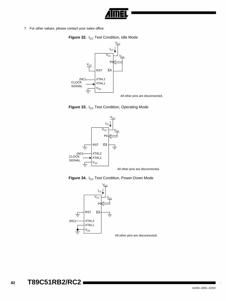
82 T89C51RB2/RC24105C–8051–02/02
7. For other values, please contact your sales office.
Figure 32. ICC Test Condition, Idle Mode
Figure 33. ICC Test Condition, Operating Mode
Figure 34. ICC Test Condition, Power-Down Mode
EA
VCC
VCC
ICC
(NC)CLOCKSIGNAL
VCC
All other pins are disconnected.
RST
XTAL2XTAL1
VSS
VCC
P0
RST EA
XTAL2XTAL1
VSS
VCC
VCC
ICC
(NC)
P0
VCC
All other pins are disconnected.
CLOCKSIGNAL
RST EA
XTAL2XTAL1
VSS
VCC
VCC
ICC
(NC)
P0
VCC
All other pins are disconnected.
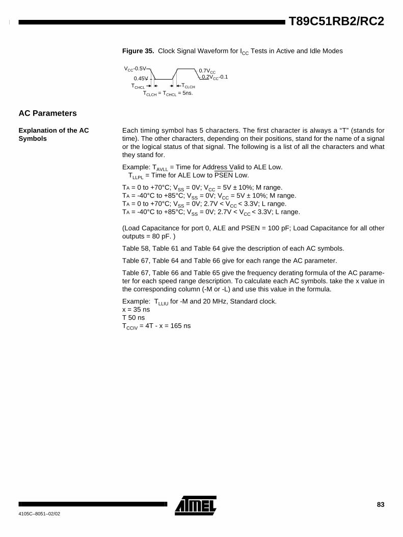
83
T89C51RB2/RC2
4105C–8051–02/02
Figure 35. Clock Signal Waveform for ICC Tests in Active and Idle Modes
AC Parameters
Explanation of the ACSymbols
Each timing symbol has 5 characters. The first character is always a “T” (stands fortime). The other characters, depending on their positions, stand for the name of a signalor the logical status of that signal. The following is a list of all the characters and whatthey stand for.
Example: TAVLL = Time for Address Valid to ALE Low.TLLPL = Time for ALE Low to PSEN Low.
TA = 0 to +70°C; VSS = 0V; VCC = 5V ± 10%; M range.TA = -40°C to +85°C; VSS = 0V; VCC = 5V ± 10%; M range.TA = 0 to +70°C; VSS = 0V; 2.7V < VCC < 3.3V; L range.TA = -40°C to +85°C; VSS = 0V; 2.7V < VCC < 3.3V; L range.
(Load Capacitance for port 0, ALE and PSEN = 100 pF; Load Capacitance for all otheroutputs = 80 pF. )
Table 58, Table 61 and Table 64 give the description of each AC symbols.
Table 67, Table 64 and Table 66 give for each range the AC parameter.
Table 67, Table 66 and Table 65 give the frequency derating formula of the AC parame-ter for each speed range description. To calculate each AC symbols. take the x value inthe corresponding column (-M or -L) and use this value in the formula.
Example: TLLIU for -M and 20 MHz, Standard clock.x = 35 nsT 50 nsTCCIV = 4T - x = 165 ns
VCC-0.5V
0.45V
0.7VCC0.2VCC-0.1
TCLCHTCHCL
TCLCH = TCHCL = 5ns.
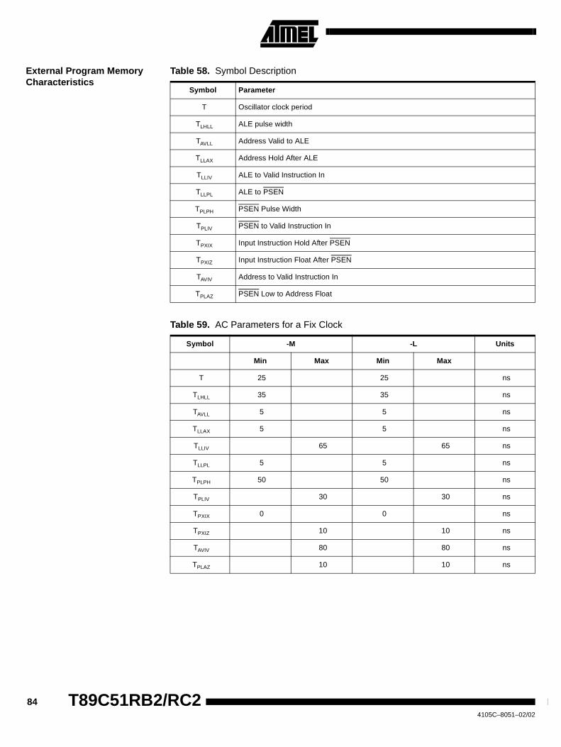
84 T89C51RB2/RC24105C–8051–02/02
External Program MemoryCharacteristics
Table 58. Symbol Description
Table 59. AC Parameters for a Fix Clock
Symbol Parameter
T Oscillator clock period
TLHLL ALE pulse width
TAVLL Address Valid to ALE
TLLAX Address Hold After ALE
TLLIV ALE to Valid Instruction In
TLLPL ALE to PSEN
TPLPH PSEN Pulse Width
TPLIV PSEN to Valid Instruction In
TPXIX Input Instruction Hold After PSEN
TPXIZ Input Instruction Float After PSEN
TAVIV Address to Valid Instruction In
TPLAZ PSEN Low to Address Float
Symbol -M -L Units
Min Max Min Max
T 25 25 ns
TLHLL 35 35 ns
TAVLL 5 5 ns
TLLAX 5 5 ns
TLLIV 65 65 ns
TLLPL 5 5 ns
TPLPH 50 50 ns
TPLIV 30 30 ns
TPXIX 0 0 ns
TPXIZ 10 10 ns
TAVIV 80 80 ns
TPLAZ 10 10 ns
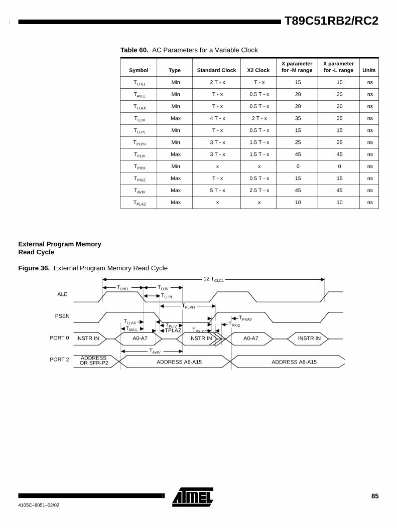
85
T89C51RB2/RC2
4105C–8051–02/02
Table 60. AC Parameters for a Variable Clock
External Program MemoryRead Cycle
Figure 36. External Program Memory Read Cycle
Symbol Type Standard Clock X2 ClockX parameterfor -M range
X parameterfor -L range Units
TLHLL Min 2 T - x T - x 15 15 ns
TAVLL Min T - x 0.5 T - x 20 20 ns
TLLAX Min T - x 0.5 T - x 20 20 ns
TLLIV Max 4 T - x 2 T - x 35 35 ns
TLLPL Min T - x 0.5 T - x 15 15 ns
TPLPH Min 3 T - x 1.5 T - x 25 25 ns
TPLIV Max 3 T - x 1.5 T - x 45 45 ns
TPXIX Min x x 0 0 ns
TPXIZ Max T - x 0.5 T - x 15 15 ns
TAVIV Max 5 T - x 2.5 T - x 45 45 ns
TPLAZ Max x x 10 10 ns
TPLIVTPLAZ
ALE
PSEN
PORT 0
PORT 2
A0-A7A0-A7 INSTR ININSTR IN INSTR IN
ADDRESSOR SFR-P2 ADDRESS A8-A15ADDRESS A8-A15
12 TCLCL
TAVIV
TLHLL
TAVLL
TLLIV
TLLPL
TPLPH
TPXAV
TPXIX
TPXIZTLLAX
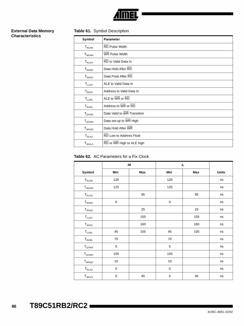
86 T89C51RB2/RC24105C–8051–02/02
External Data MemoryCharacteristics
Table 61. Symbol Description
Table 62. AC Parameters for a Fix Clock
Symbol Parameter
TRLRH RD Pulse Width
TWLWH WR Pulse Width
TRLDV RD to Valid Data In
TRHDX Data Hold After RD
TRHDZ Data Float After RD
TLLDV ALE to Valid Data In
TAVDV Address to Valid Data In
TLLWL ALE to WR or RD
TAVWL Address to WR or RD
TQVWX Data Valid to WR Transition
TQVWH Data set-up to WR High
TWHQX Data Hold After WR
TRLAZ RD Low to Address Float
TWHLH RD or WR High to ALE high
Symbol
-M -L
UnitsMin Max Min Max
TRLRH 125 125 ns
TWLWH 125 125 ns
TRLDV 95 95 ns
TRHDX 0 0 ns
TRHDZ 25 25 ns
TLLDV 155 155 ns
TAVDV 160 160 ns
TLLWL 45 105 45 105 ns
TAVWL 70 70 ns
TQVWX 5 5 ns
TQVWH 155 155 ns
TWHQX 10 10 ns
TRLAZ 0 0 ns
TWHLH 5 45 5 45 ns
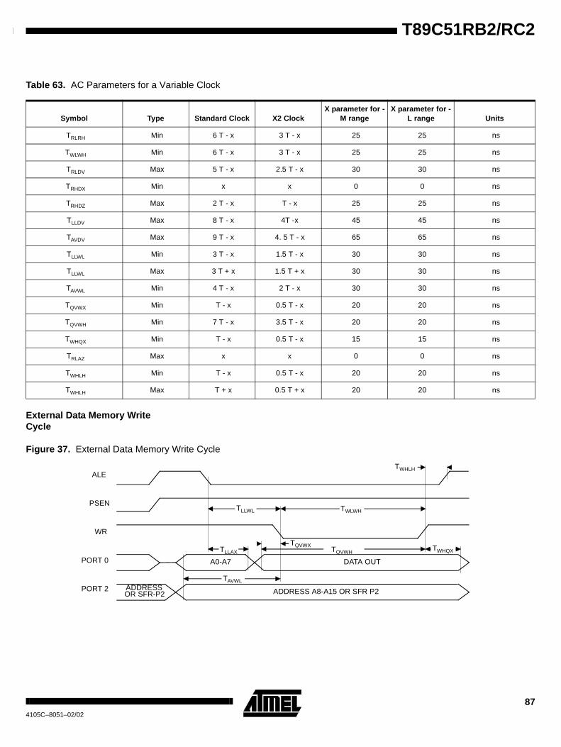
87
T89C51RB2/RC2
4105C–8051–02/02
External Data Memory WriteCycle
Figure 37. External Data Memory Write Cycle
Table 63. AC Parameters for a Variable Clock
Symbol Type Standard Clock X2 ClockX parameter for -
M rangeX parameter for -
L range Units
TRLRH Min 6 T - x 3 T - x 25 25 ns
TWLWH Min 6 T - x 3 T - x 25 25 ns
TRLDV Max 5 T - x 2.5 T - x 30 30 ns
TRHDX Min x x 0 0 ns
TRHDZ Max 2 T - x T - x 25 25 ns
TLLDV Max 8 T - x 4T -x 45 45 ns
TAVDV Max 9 T - x 4. 5 T - x 65 65 ns
TLLWL Min 3 T - x 1.5 T - x 30 30 ns
TLLWL Max 3 T + x 1.5 T + x 30 30 ns
TAVWL Min 4 T - x 2 T - x 30 30 ns
TQVWX Min T - x 0.5 T - x 20 20 ns
TQVWH Min 7 T - x 3.5 T - x 20 20 ns
TWHQX Min T - x 0.5 T - x 15 15 ns
TRLAZ Max x x 0 0 ns
TWHLH Min T - x 0.5 T - x 20 20 ns
TWHLH Max T + x 0.5 T + x 20 20 ns
TQVWHTLLAX
ALE
PSEN
WR
PORT 0
PORT 2
A0-A7 DATA OUT
ADDRESSOR SFR-P2
TAVWL
TLLWL
TQVWX
ADDRESS A8-A15 OR SFR P2
TWHQX
TWHLH
TWLWH
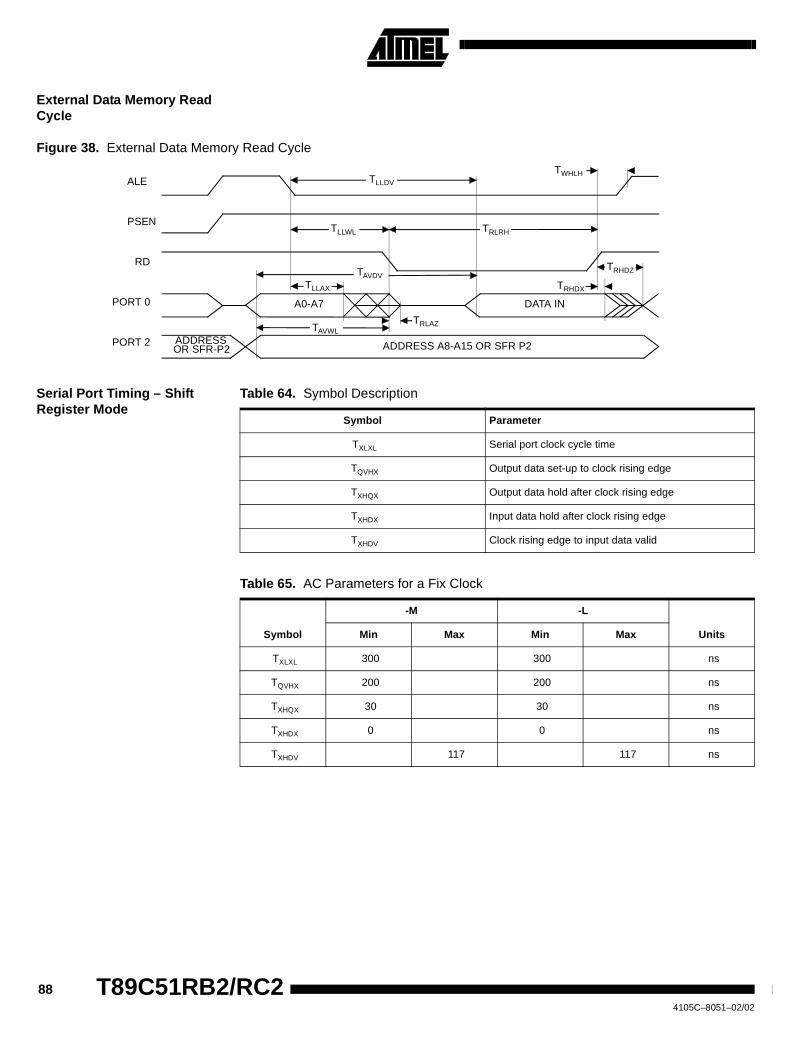
88 T89C51RB2/RC24105C–8051–02/02
External Data Memory ReadCycle
Figure 38. External Data Memory Read Cycle
Serial Port Timing – ShiftRegister Mode
Table 64. Symbol Description
Table 65. AC Parameters for a Fix Clock
ALE
PSEN
RD
PORT 0
PORT 2
A0-A7 DATA IN
ADDRESSOR SFR-P2
TAVWL
TLLWL
TRLAZ
ADDRESS A8-A15 OR SFR P2
TRHDZ
TWHLH
TRLRH
TLLDV
TRHDXTLLAX
TAVDV
Symbol Parameter
TXLXL Serial port clock cycle time
TQVHX Output data set-up to clock rising edge
TXHQX Output data hold after clock rising edge
TXHDX Input data hold after clock rising edge
TXHDV Clock rising edge to input data valid
Symbol
-M -L
UnitsMin Max Min Max
TXLXL 300 300 ns
TQVHX 200 200 ns
TXHQX 30 30 ns
TXHDX 0 0 ns
TXHDV 117 117 ns
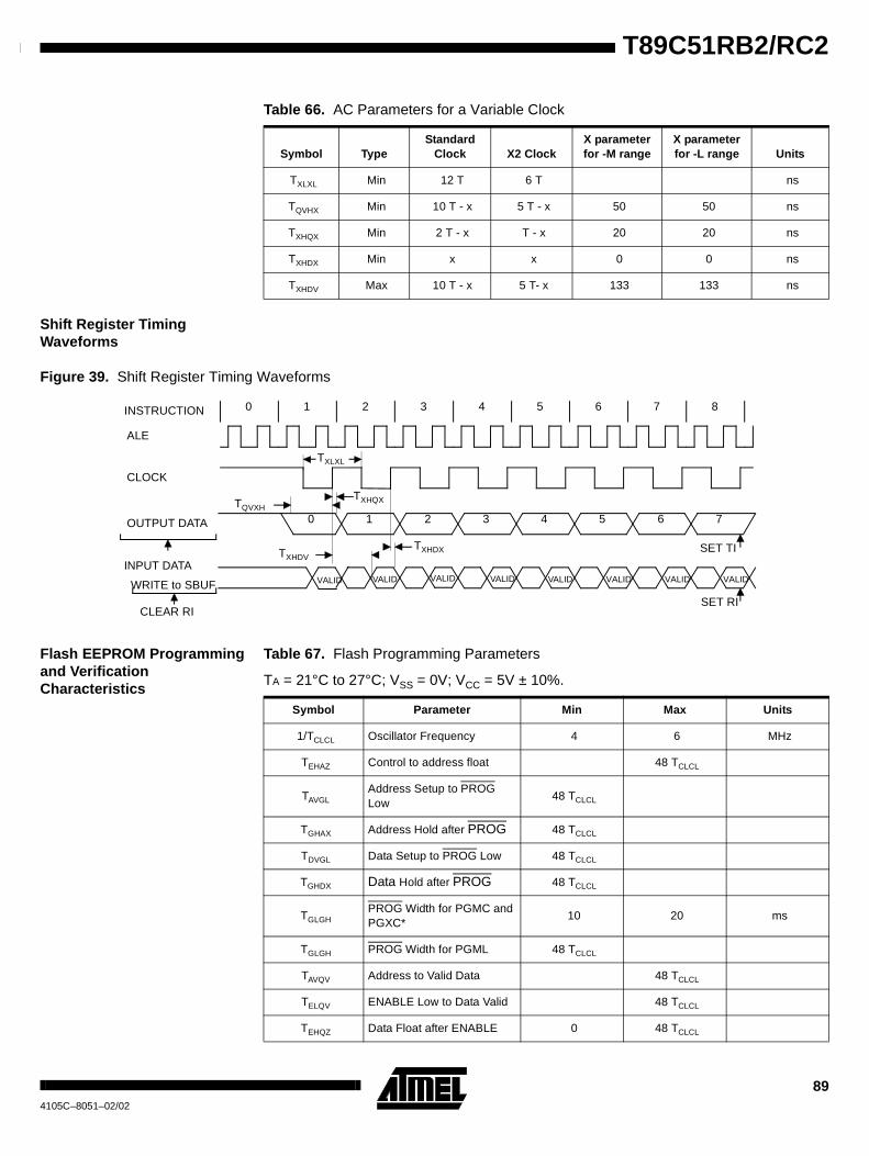
89
T89C51RB2/RC2
4105C–8051–02/02
Table 66. AC Parameters for a Variable Clock
Shift Register TimingWaveforms
Figure 39. Shift Register Timing Waveforms
Flash EEPROM Programmingand VerificationCharacteristics
Table 67. Flash Programming Parameters
TA = 21°C to 27°C; VSS = 0V; VCC = 5V ± 10%.
Symbol TypeStandard
Clock X2 ClockX parameterfor -M range
X parameterfor -L range Units
TXLXL Min 12 T 6 T ns
TQVHX Min 10 T - x 5 T - x 50 50 ns
TXHQX Min 2 T - x T - x 20 20 ns
TXHDX Min x x 0 0 ns
TXHDV Max 10 T - x 5 T- x 133 133 ns
VALID
INPUT DATAVALID VALID
0 1 2 3 4 5 6 87
ALE
CLOCK
OUTPUT DATA
WRITE to SBUF
CLEAR RI
TXLXL
TQVXHTXHQX
TXHDVTXHDX SET TI
SET RI
INSTRUCTION
0 1 2 3 4 5 6 7
VALID VALID VALID VALIDVALID
Symbol Parameter Min Max Units
1/TCLCL Oscillator Frequency 4 6 MHz
TEHAZ Control to address float 48 TCLCL
TAVGLAddress Setup to PROGLow
48 TCLCL
TGHAX Address Hold after PROG 48 TCLCL
TDVGL Data Setup to PROG Low 48 TCLCL
TGHDX Data Hold after PROG 48 TCLCL
TGLGHPROG Width for PGMC andPGXC*
10 20 ms
TGLGH PROG Width for PGML 48 TCLCL
TAVQV Address to Valid Data 48 TCLCL
TELQV ENABLE Low to Data Valid 48 TCLCL
TEHQZ Data Float after ENABLE 0 48 TCLCL
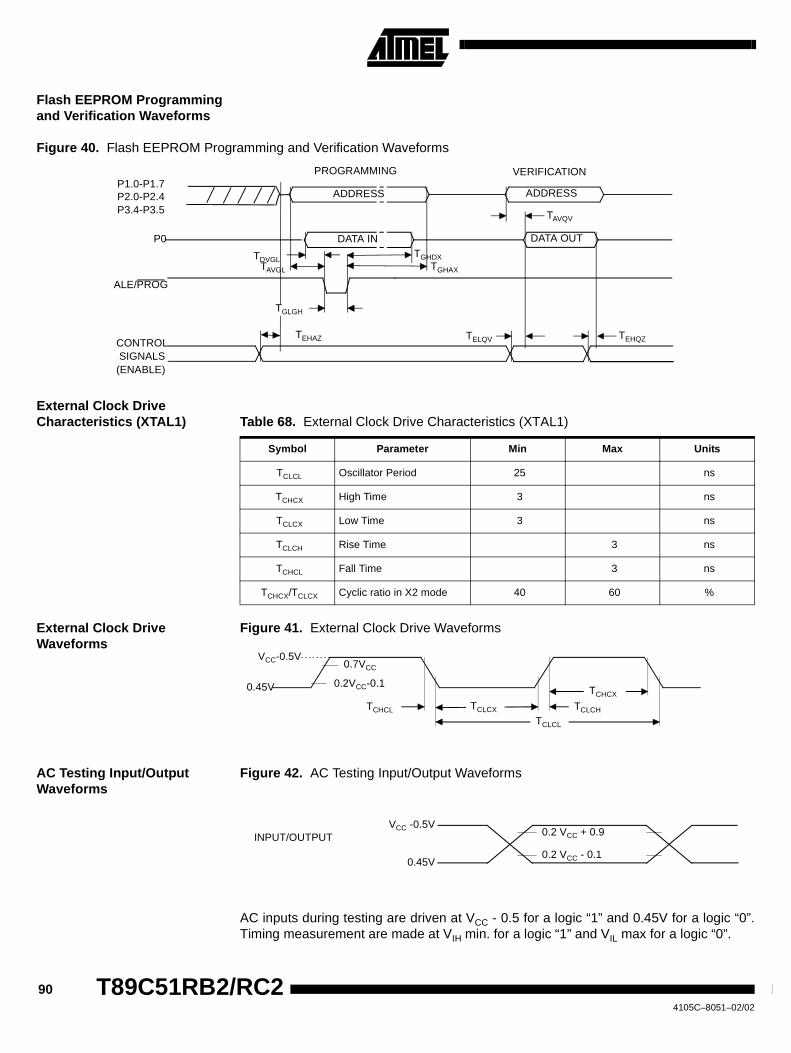
90 T89C51RB2/RC24105C–8051–02/02
Flash EEPROM Programmingand Verification Waveforms
Figure 40. Flash EEPROM Programming and Verification Waveforms
External Clock DriveCharacteristics (XTAL1) Table 68. External Clock Drive Characteristics (XTAL1)
External Clock DriveWaveforms
Figure 41. External Clock Drive Waveforms
AC Testing Input/OutputWaveforms
Figure 42. AC Testing Input/Output Waveforms
AC inputs during testing are driven at VCC - 0.5 for a logic “1” and 0.45V for a logic “0”.Timing measurement are made at VIH min. for a logic “1” and VIL max for a logic “0”.
TEHAZ
ALE/PROG
TAVGL
TDVGL
P0
P1.0-P1.7P2.0-P2.4P3.4-P3.5
CONTROLSIGNALS(ENABLE)
ADDRESS
DATA IN
TGHAX
TGHDX
TGLGH
ADDRESS
DATA OUT
TAVQV
TELQV TEHQZ
PROGRAMMING VERIFICATION
Symbol Parameter Min Max Units
TCLCL Oscillator Period 25 ns
TCHCX High Time 3 ns
TCLCX Low Time 3 ns
TCLCH Rise Time 3 ns
TCHCL Fall Time 3 ns
TCHCX/TCLCX Cyclic ratio in X2 mode 40 60 %
VCC-0.5V
0.45V
0.7VCC
0.2VCC-0.1
TCHCL TCLCX
TCLCL
TCLCH
TCHCX
INPUT/OUTPUT 0.2 VCC + 0.9
0.2 VCC - 0.1
VCC -0.5V
0.45V
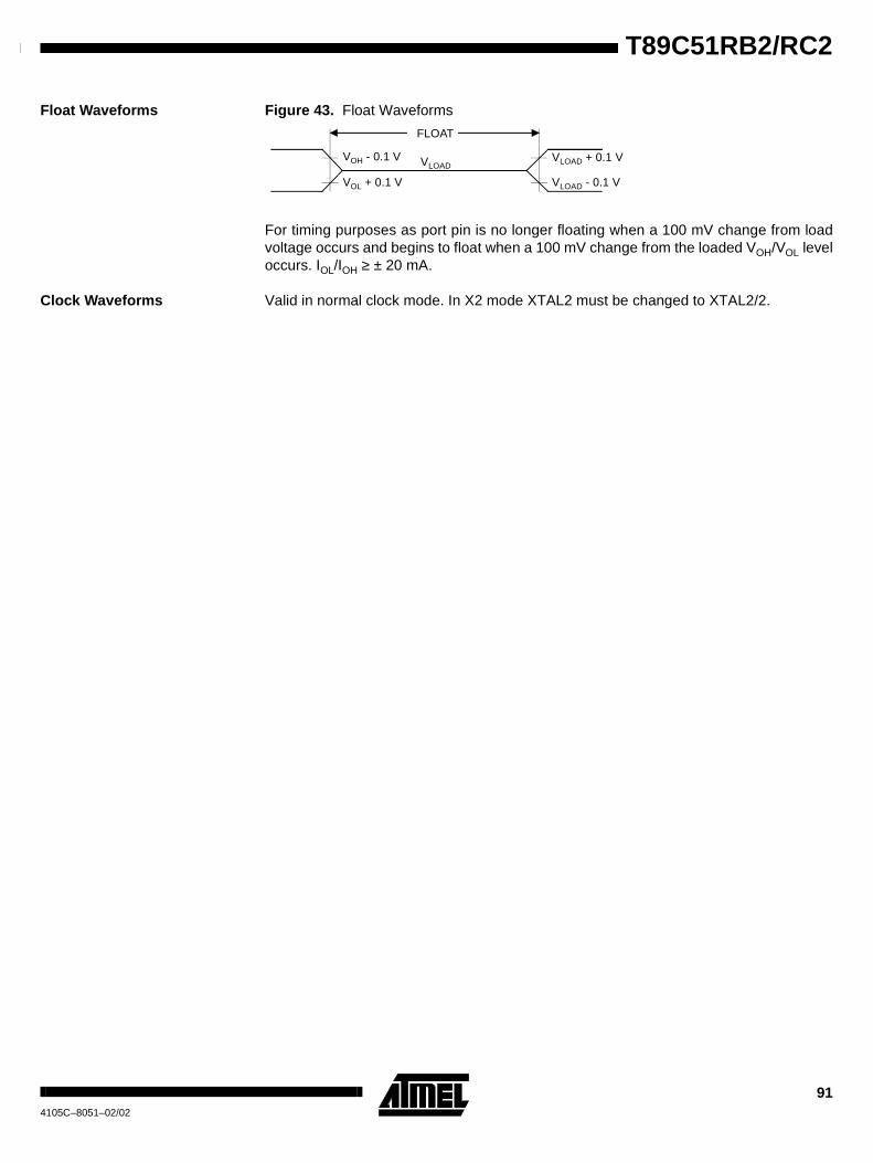
91
T89C51RB2/RC2
4105C–8051–02/02
Float Waveforms Figure 43. Float Waveforms
For timing purposes as port pin is no longer floating when a 100 mV change from loadvoltage occurs and begins to float when a 100 mV change from the loaded VOH/VOL leveloccurs. IOL/IOH ≥ ± 20 mA.
Clock Waveforms Valid in normal clock mode. In X2 mode XTAL2 must be changed to XTAL2/2.
FLOAT
VOH - 0.1 V
VOL + 0.1 V
VLOADVLOAD + 0.1 V
VLOAD - 0.1 V
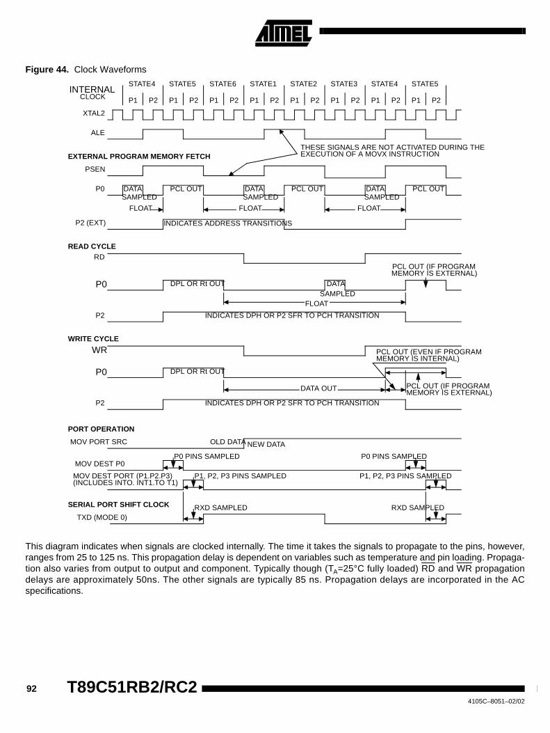
92 T89C51RB2/RC24105C–8051–02/02
Figure 44. Clock Waveforms
This diagram indicates when signals are clocked internally. The time it takes the signals to propagate to the pins, however,ranges from 25 to 125 ns. This propagation delay is dependent on variables such as temperature and pin loading. Propaga-tion also varies from output to output and component. Typically though (TA=25°C fully loaded) RD and WR propagationdelays are approximately 50ns. The other signals are typically 85 ns. Propagation delays are incorporated in the ACspecifications.
P2 (EXT)
DATA PCL OUT DATA PCL OUT DATA PCL OUTSAMPLED SAMPLED SAMPLED
STATE4 STATE5 STATE6 STATE1 STATE2 STATE3 STATE4 STATE5
P1 P2 P1 P2 P1 P2 P1 P2 P1 P2 P1 P2 P1 P2 P1 P2
FLOAT FLOAT FLOAT
THESE SIGNALS ARE NOT ACTIVATED DURING THEEXECUTION OF A MOVX INSTRUCTION
INDICATES ADDRESS TRANSITIONS
EXTERNAL PROGRAM MEMORY FETCH
FLOAT
DATASAMPLED
DPL OR Rt OUT
INDICATES DPH OR P2 SFR TO PCH TRANSITION
PCL OUT (IF PROGRAMMEMORY IS EXTERNAL)
PCL OUT (EVEN IF PROGRAMMEMORY IS INTERNAL)
PCL OUT (IF PROGRAMMEMORY IS EXTERNAL)
OLD DATA NEW DATA
P0 PINS SAMPLED
P1, P2, P3 PINS SAMPLED P1, P2, P3 PINS SAMPLED
P0 PINS SAMPLED
RXD SAMPLED
INTERNALCLOCK
XTAL2
ALE
PSEN
P0
READ CYCLE
WRITE CYCLE
RD
P0
P2
WR
PORT OPERATION
MOV PORT SRC
MOV DEST P0
MOV DEST PORT (P1.P2.P3)(INCLUDES INTO. INT1.TO T1)
SERIAL PORT SHIFT CLOCK
TXD (MODE 0)
DATA OUT
DPL OR Rt OUT
INDICATES DPH OR P2 SFR TO PCH TRANSITION
P0
P2
RXD SAMPLED
93
T89C51RB2/RC2
4105C–8051–02/02
Flash EEPROMMemory
The Flash memory increases EPROM and ROM functionality with in-circuit electricalerasure and programming. It contains 16K or 32K bytes of program memory organizedrespectively in 128 or 256 pages of 128 bytes. This memory is both parallel and serialIn-System Programmable (ISP). ISP allows devices to alter their own program memoryin the actual end product under software control. A default serial loader (bootloader) pro-gram allows ISP of the Flash.
The programming does not require 12V external programming voltage. The necessaryhigh programming voltage is generated on-chip using the standard VCC pins of themicrocontroller.
Features • Flash E2PROM internal program memory.
• Boot vector allows user provided Flash loader code to reside anywhere in the Flashmemory space. This configuration provides flexibility to the user.
• Default loader in Boot ROM allows programming via the serial port without the needof a user provided loader.
• Up to 64K byte external program memory if the internal program memory is disabled(EA = 0).
• Programming and erase voltage with standard 5V or 3V VCC supply.
• Read/Programming/Erase:
• Byte-wise read without wait state
• Byte or page erase and programming (10 ms)
• Typical programming time (32K bytes) in 10s
• Parallel programming with 87C51 compatible hardware interface to programmer
• Programmable security for the code in the Flash
• 10k write cycles
• 10 years data retention
Flash Programming andErasure
The 16K or 32K bytes Flash is programmed by bytes or by pages of 128 bytes. It is notnecessary to erase a byte or a page before programming. The programming of a byte ora page includes a self erase before programming.
There are three methods of programming the Flash memory:
• First, the on-chip ISP bootloader may be invoked which will use low level routines toprogram the pages. The interface used for serial downloading of Flash is the UART.
• Second, the Flash may be programmed or erased in the end-user application bycalling low-level routines through a common entry point in the Boot ROM.
• Third, the Flash may be programmed using the parallel method by using aconventional EPROM programmer. The parallel programming method used bythese devices is similar to that used by EPROM 87C51 but it is not identical and thecommercially available programmers need to have support for theT89C51RB2/RC2. The bootloader and the Application Programming Interface (API)routines are located in the BOOT ROM.
94 T89C51RB2/RC24105C–8051–02/02
Flash Registers andMemory Map
The T89C51RB2/RC2 Flash memory uses several registers for his management:
• Hardware registers can only be accessed through the parallel programming modeswhich are handled by the parallel programmer.
• Software registers are in a special page of the Flash memory which can beaccessed through the API or with the parallel programming modes. This page,called "Extra Flash Memory", is not in the internal Flash program memoryaddressing space.
Hardware Register The only hardware register of the T89C51RB2/RC2 is called Hardware Security Byte(HSB).
Table 69. Hardware Security Byte (HSB)
Boot Loader Jump Bit (BLJB)
One bit of the HSB, the BLJB bit, is used to force the boot address:
• When this bit is set the boot address is 0000h.
• When this bit is reset the boot address is F800h. By default, this bit is cleared andthe ISP is enabled.
Flash Memory Lock Bits The three lock bits provide different levels of protection for the on-chip code and data,when programmed as shown in Table 70.
7 6 5 4 3 2 1 0
X2 BLJB - - XRAM LB2 LB1 LB0
BitNumber
BitMnemonic Description
7 X2X2 ModeProgrammed to force X2 mode (6 clocks per instruction)
Unprogrammed to force X1 mode, Standard Mode. (Default)
6 BLJB
Boot Loader Jump Bit
Unprogrammed this bit to start the user’s application on next reset at address0000h.
Programmed this bit to start the boot loader at address F800h (Default).
5 - Reserved
4 - Reserved
3 XRAM
XRAM config bit (only programmable by programmer tools)
Programmed to inhibit XRAM
Unprogrammed, this bit to valid XRAM (Default)
2-0 LB2-0User Memory Lock Bits (only programmable by programmer tools)
See Table 70
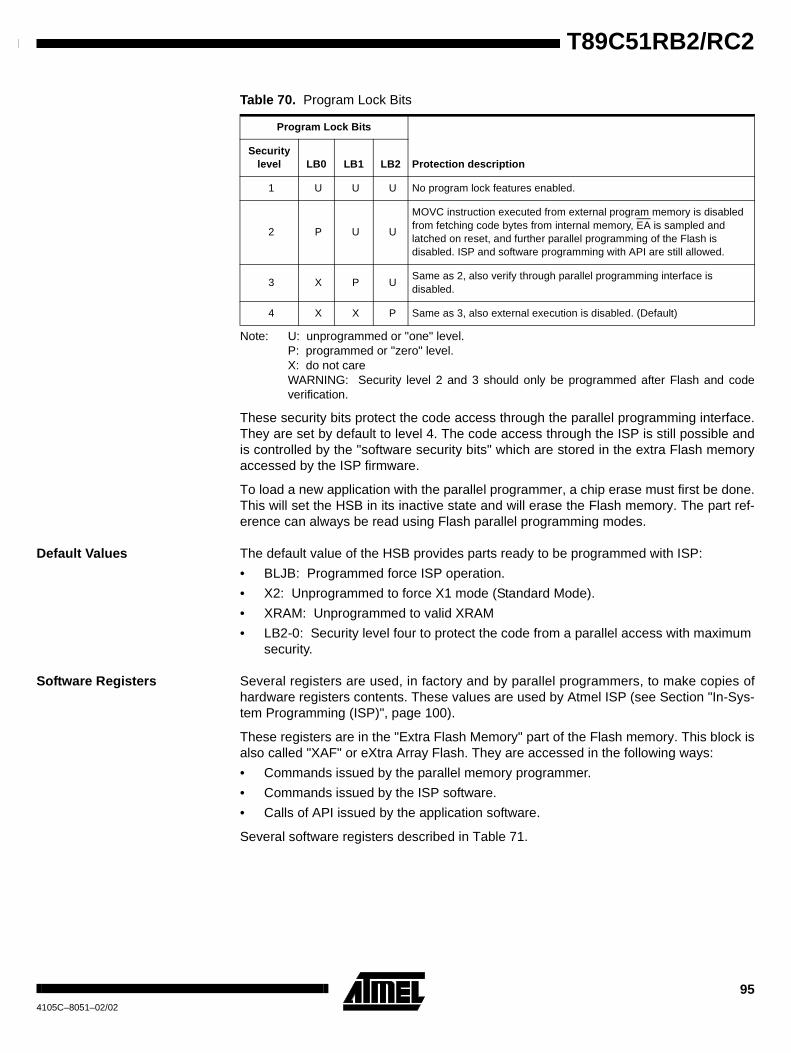
95
T89C51RB2/RC2
4105C–8051–02/02
Table 70. Program Lock Bits
Note: U: unprogrammed or "one" level.P: programmed or "zero" level.X: do not careWARNING: Security level 2 and 3 should only be programmed after Flash and codeverification.
These security bits protect the code access through the parallel programming interface.They are set by default to level 4. The code access through the ISP is still possible andis controlled by the "software security bits" which are stored in the extra Flash memoryaccessed by the ISP firmware.
To load a new application with the parallel programmer, a chip erase must first be done.This will set the HSB in its inactive state and will erase the Flash memory. The part ref-erence can always be read using Flash parallel programming modes.
Default Values The default value of the HSB provides parts ready to be programmed with ISP:
• BLJB: Programmed force ISP operation.
• X2: Unprogrammed to force X1 mode (Standard Mode).
• XRAM: Unprogrammed to valid XRAM
• LB2-0: Security level four to protect the code from a parallel access with maximumsecurity.
Software Registers Several registers are used, in factory and by parallel programmers, to make copies ofhardware registers contents. These values are used by Atmel ISP (see Section "In-Sys-tem Programming (ISP)", page 100).
These registers are in the "Extra Flash Memory" part of the Flash memory. This block isalso called "XAF" or eXtra Array Flash. They are accessed in the following ways:
• Commands issued by the parallel memory programmer.
• Commands issued by the ISP software.
• Calls of API issued by the application software.
Several software registers described in Table 71.
Program Lock Bits
Protection descriptionSecurity
level LB0 LB1 LB2
1 U U U No program lock features enabled.
2 P U U
MOVC instruction executed from external program memory is disabledfrom fetching code bytes from internal memory, EA is sampled andlatched on reset, and further parallel programming of the Flash isdisabled. ISP and software programming with API are still allowed.
3 X P USame as 2, also verify through parallel programming interface isdisabled.
4 X X P Same as 3, also external execution is disabled. (Default)
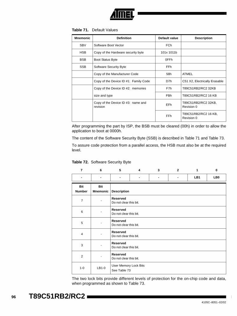
96 T89C51RB2/RC24105C–8051–02/02
Table 71. Default Values
After programming the part by ISP, the BSB must be cleared (00h) in order to allow theapplication to boot at 0000h.
The content of the Software Security Byte (SSB) is described in Table 71 and Table 73.
To assure code protection from a parallel access, the HSB must also be at the requiredlevel.
Table 72. Software Security Byte
The two lock bits provide different levels of protection for the on-chip code and data,when programmed as shown to Table 73.
Mnemonic Definition Default value Description
SBV Software Boot Vector FCh
HSB Copy of the Hardware security byte 101x 1011b
BSB Boot Status Byte 0FFh
SSB Software Security Byte FFh
Copy of the Manufacturer Code 58h ATMEL
Copy of the Device ID #1: Family Code D7h C51 X2, Electrically Erasable
Copy of the Device ID #2: memories F7h T89C51RB2/RC2 32KB
size and type FBh T89C51RB2/RC2 16 KB
Copy of the Device ID #3: name andrevision
EFhT89C51RB2/RC2 32KB,Revision 0
FFhT89C51RB2/RC2 16 KB,Revision 0
7 6 5 4 3 2 1 0
- - - - - - LB1 LB0
Bit
Number
Bit
Mnemonic Description
7 -ReservedDo not clear this bit.
6 -ReservedDo not clear this bit.
5 -ReservedDo not clear this bit.
4 -ReservedDo not clear this bit.
3 -ReservedDo not clear this bit.
2 -ReservedDo not clear this bit.
1-0 LB1-0User Memory Lock Bits
See Table 73
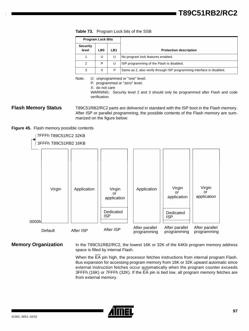
97
T89C51RB2/RC2
4105C–8051–02/02
Table 73. Program Lock bits of the SSB
Note: U: unprogrammed or "one" level.P: programmed or "zero" level.X: do not careWARNING: Security level 2 and 3 should only be programmed after Flash and codeverification.
Flash Memory Status T89C51RB2/RC2 parts are delivered in standard with the ISP boot in the Flash memory.After ISP or parallel programming, the possible contents of the Flash memory are sum-marized on the figure below:
Figure 45. Flash memory possible contents
Memory Organization In the T89C51RB2/RC2, the lowest 16K or 32K of the 64Kb program memory addressspace is filled by internal Flash.
When the EA pin high, the processor fetches instructions from internal program Flash.Bus expansion for accessing program memory from 16K or 32K upward automatic sinceexternal instruction fetches occur automatically when the program counter exceeds3FFFh (16K) or 7FFFh (32K). If the EA pin is tied low, all program memory fetches arefrom external memory.
Program Lock Bits
Protection descriptionSecurity
level LB0 LB1
1 U U No program lock features enabled.
2 P U ISP programming of the Flash is disabled.
3 X P Same as 2, also verify through ISP programming interface is disabled.
0000h
Virgin
3FFFh
Default After ISPAfter parallelprogramming
After parallelprogramming
After parallelprogramming
ApplicationApplication Virgin
After ISP
or
DedicatedISP
DedicatedISP
7FFFh T89C51RC2 32KB
T89C51RB2 16KB
application
Virginor
application
Virginor
application
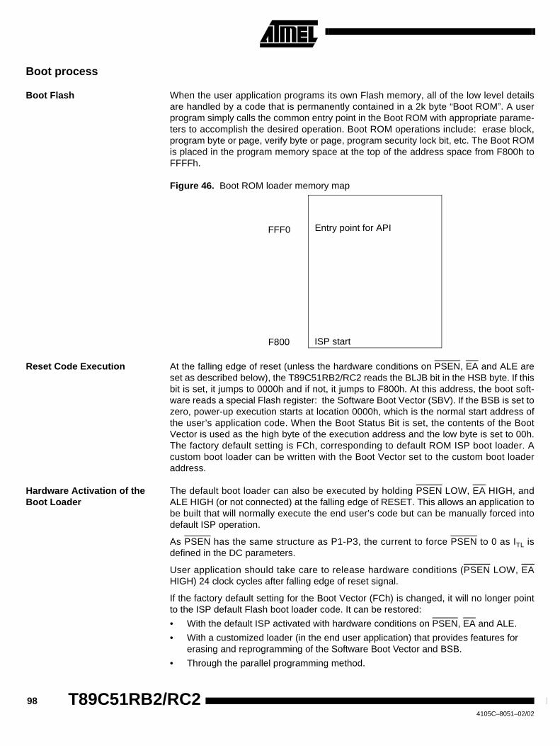
98 T89C51RB2/RC24105C–8051–02/02
Boot process
Boot Flash When the user application programs its own Flash memory, all of the low level detailsare handled by a code that is permanently contained in a 2k byte “Boot ROM”. A userprogram simply calls the common entry point in the Boot ROM with appropriate parame-ters to accomplish the desired operation. Boot ROM operations include: erase block,program byte or page, verify byte or page, program security lock bit, etc. The Boot ROMis placed in the program memory space at the top of the address space from F800h toFFFFh.
Figure 46. Boot ROM loader memory map
Reset Code Execution At the falling edge of reset (unless the hardware conditions on PSEN, EA and ALE areset as described below), the T89C51RB2/RC2 reads the BLJB bit in the HSB byte. If thisbit is set, it jumps to 0000h and if not, it jumps to F800h. At this address, the boot soft-ware reads a special Flash register: the Software Boot Vector (SBV). If the BSB is set tozero, power-up execution starts at location 0000h, which is the normal start address ofthe user’s application code. When the Boot Status Bit is set, the contents of the BootVector is used as the high byte of the execution address and the low byte is set to 00h.The factory default setting is FCh, corresponding to default ROM ISP boot loader. Acustom boot loader can be written with the Boot Vector set to the custom boot loaderaddress.
Hardware Activation of theBoot Loader
The default boot loader can also be executed by holding PSEN LOW, EA HIGH, andALE HIGH (or not connected) at the falling edge of RESET. This allows an application tobe built that will normally execute the end user’s code but can be manually forced intodefault ISP operation.
As PSEN has the same structure as P1-P3, the current to force PSEN to 0 as ITL isdefined in the DC parameters.
User application should take care to release hardware conditions (PSEN LOW, EAHIGH) 24 clock cycles after falling edge of reset signal.
If the factory default setting for the Boot Vector (FCh) is changed, it will no longer pointto the ISP default Flash boot loader code. It can be restored:
• With the default ISP activated with hardware conditions on PSEN, EA and ALE.
• With a customized loader (in the end user application) that provides features forerasing and reprogramming of the Software Boot Vector and BSB.
• Through the parallel programming method.
FFF0 Entry point for API
ISP startF800
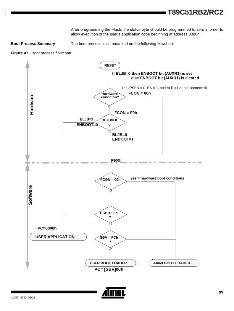
99
T89C51RB2/RC2
4105C–8051–02/02
After programming the Flash, the status byte should be programmed to zero in order toallow execution of the user’s application code beginning at address 0000h.
Boot Process Summary The boot process is summarized on the following flowchart:
Figure 47. Boot process flowchart
RESET
Hardwarecondition?
BLJB!= 0?
USER APPLICATION
Har
dw
are
So
ftw
are
FCON = 00h
FCON = F0h
FCON = 00h?
Atmel BOOT LOADERUSER BOOT LOADER
yes = hardware boot
F800h
BLJB=1
BSB = 00h?
SBV = FCh?
PC=0000h
PC= [SBV]00h
conditions
BLJB=0
If BLJB=0 then ENBOOT bit (AUXR1) is setelse ENBOOT bit (AUXR1) is cleared
ENBOOT=1
ENBOOT=0
Yes (PSEN = 0, EA = 1, and ALE =1 or not connected)
100 T89C51RB2/RC24105C–8051–02/02
In-System Programming(ISP)
The In-System Programming (ISP) is performed without removing the microcontrollerfrom the system. The ISP facility consists of a series of internal hardware resourcescoupled with internal firmware to facilitate remote programming of theT89C51RB2/RC2through the serial port.
The Atmel ISP facility has made in-circuit programming in an embedded applicationpossible with a minimum of additional expense in components and circuit board area.
The ISP function through UART uses four pins: TxD, RxD, VSS, VCC. Only a small con-nector needs to be available to interface the application to an external circuit in order touse this feature.
Using In-SystemProgramming (ISP)
The ISP feature allows a wide range of baud rates in the user application. It is alsoadaptable to a wide range of oscillator frequencies. This is accomplished by measuringthe bit-time of a single bit in a received character. This information is then used to pro-gram the baud rate in terms of timer counts based on the oscillator frequency. The ISPfeature requires that an ini t ial character (an uppercase U) be sent to theT89C51RB2/RC2 to establish the baud rate. The ISP firmware provides auto-echo ofreceived characters.
Once baud rate initialization has been performed, the ISP firmware will only accept IntelHex-type records. Intel Hex records consist of ASCII characters used to represent hexa-decimal values and are summarized below:
:NNAAAARRDD. DDCC
T89C51RB2/RC2 will accept up to 16 (10h) data bytes. The “AAAA” string representsthe address of the first byte in the record. If there are zero bytes in the record, this fieldis often set to ‘‘0000’’. The “RR” string indicates the record type. A record type of “00” isa data record. A record type of “01” indicates the end-of-file mark. In this application,additional record types will be added to indicate either commands or data for the ISPfacility. The “DD” string represents the data bytes. The maximum number of data bytesin a record is limited to 16 (decimal). The “CC” string represents the checksum byte. ISPcommands are summarized in Table 74.
As a record is received by the T89C51RB2/RC2, the information in the record is storedinternally and a checksum calculation is performed and compared to ‘‘CC’’.
The operation indicated by the record type is not performed until the entire record hasbeen received. Should an error occur in the checksum, the T89C51RB2/RC2 will sendan “X” out the serial port indicating a checksum error. If the checksum calculation isfound to match the checksum in the record, then the command will be executed. In mostcases, successful reception of the record will be indicated by transmitting a “. ” characterout the serial port (displaying the contents of the internal program memory is an excep-tion). In the case of a Data Record (record type ‘‘00’’), an additional check is made. A “.” character will NOT be sent unless the record checksum matched the calculated check-sum and all of the bytes in the record were successfully programmed. For a data record,an “X” indicates that the checksum failed to match, and an “R” character indicates thatone of the bytes did not properly program.
FLIP, a software utility to implement ISP programming with a PC, is available from theAtmel the web site.
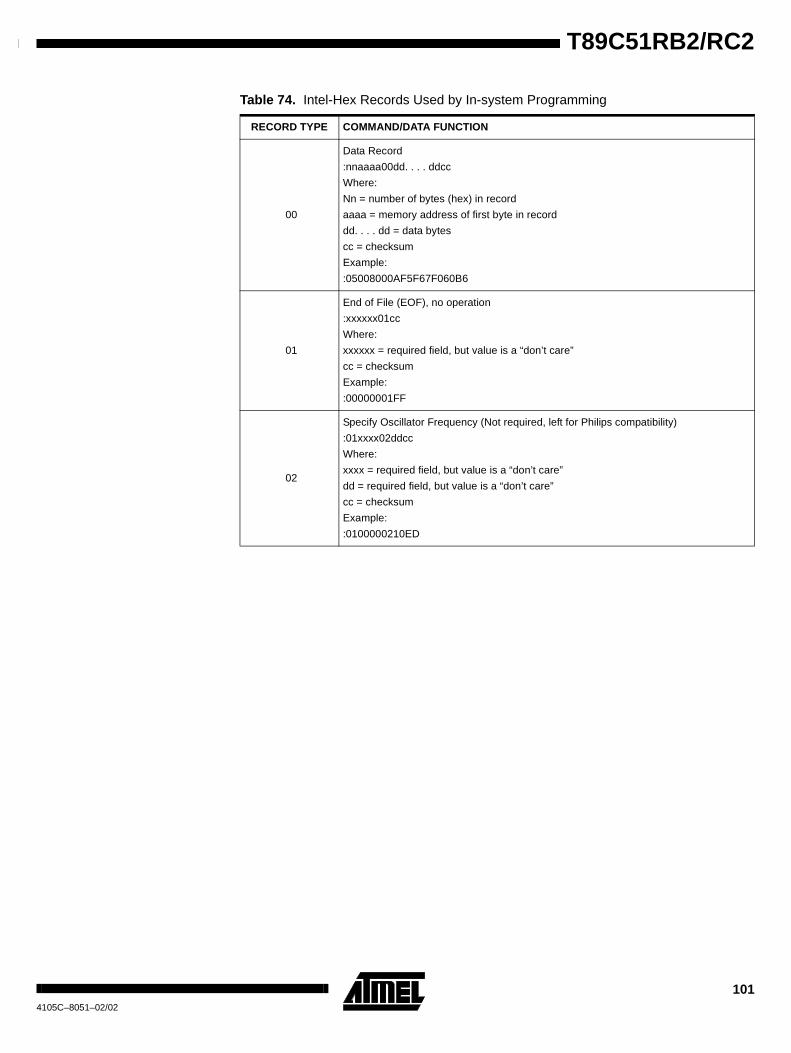
101
T89C51RB2/RC2
4105C–8051–02/02
Table 74. Intel-Hex Records Used by In-system Programming
RECORD TYPE COMMAND/DATA FUNCTION
00
Data Record
:nnaaaa00dd. . . . ddcc
Where:
Nn = number of bytes (hex) in record
aaaa = memory address of first byte in record
dd. . . . dd = data bytes
cc = checksum
Example:
:05008000AF5F67F060B6
01
End of File (EOF), no operation
:xxxxxx01cc
Where:
xxxxxx = required field, but value is a “don’t care”
cc = checksum
Example:
:00000001FF
02
Specify Oscillator Frequency (Not required, left for Philips compatibility)
:01xxxx02ddcc
Where:
xxxx = required field, but value is a “don’t care”
dd = required field, but value is a “don’t care”
cc = checksum
Example:
:0100000210ED
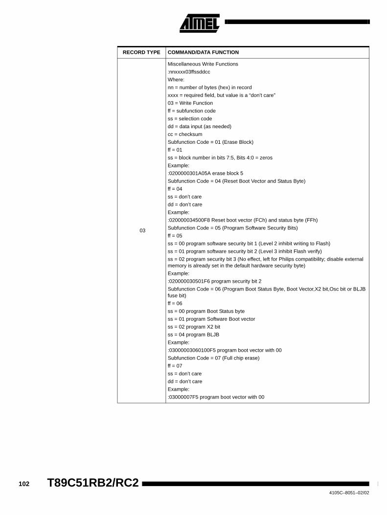
102 T89C51RB2/RC24105C–8051–02/02
03
Miscellaneous Write Functions
:nnxxxx03ffssddcc
Where:
nn = number of bytes (hex) in record
xxxx = required field, but value is a “don’t care”
03 = Write Function
ff = subfunction code
ss = selection code
dd = data input (as needed)
cc = checksum
Subfunction Code = 01 (Erase Block)
ff = 01
ss = block number in bits 7:5, Bits 4:0 = zeros
Example:
:0200000301A05A erase block 5
Subfunction Code = 04 (Reset Boot Vector and Status Byte)
ff = 04
ss = don’t care
dd = don’t care
Example:
:020000034500F8 Reset boot vector (FCh) and status byte (FFh)
Subfunction Code = 05 (Program Software Security Bits)
ff = 05
ss = 00 program software security bit 1 (Level 2 inhibit writing to Flash)
ss = 01 program software security bit 2 (Level 3 inhibit Flash verify)
ss = 02 program security bit 3 (No effect, left for Philips compatibility; disable externalmemory is already set in the default hardware security byte)
Example:
:020000030501F6 program security bit 2
Subfunction Code = 06 (Program Boot Status Byte, Boot Vector,X2 bit,Osc bit or BLJBfuse bit)
ff = 06
ss = 00 program Boot Status byte
ss = 01 program Software Boot vector
ss = 02 program X2 bit
ss = 04 program BLJB
Example:
:03000003060100F5 program boot vector with 00
Subfunction Code = 07 (Full chip erase)
ff = 07
ss = don’t care
dd = don’t care
Example:
:03000007F5 program boot vector with 00
RECORD TYPE COMMAND/DATA FUNCTION
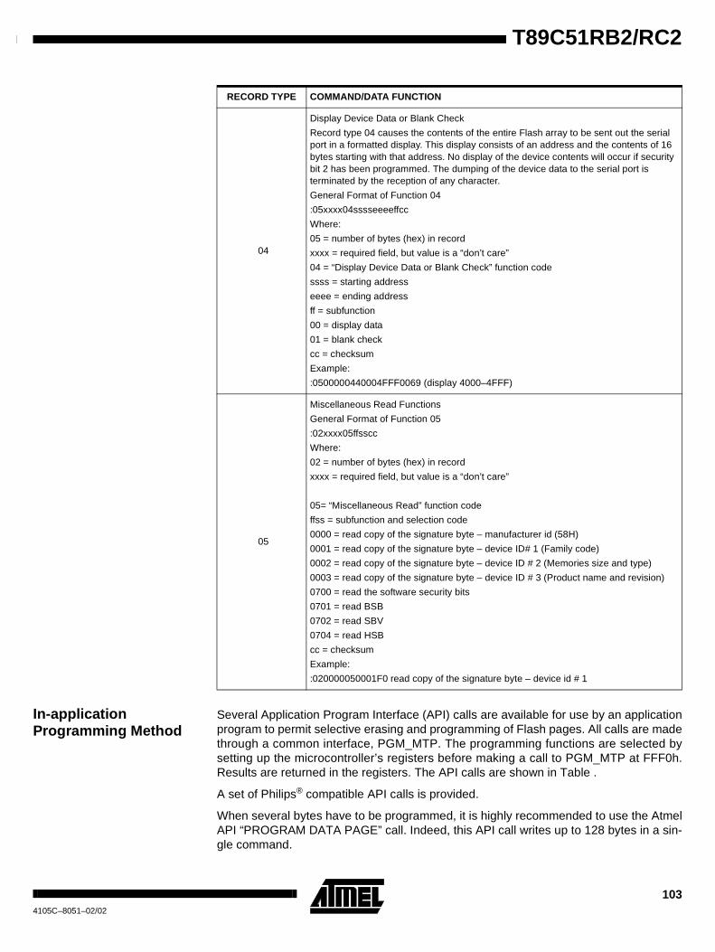
103
T89C51RB2/RC2
4105C–8051–02/02
In-applicationProgramming Method
Several Application Program Interface (API) calls are available for use by an applicationprogram to permit selective erasing and programming of Flash pages. All calls are madethrough a common interface, PGM_MTP. The programming functions are selected bysetting up the microcontroller’s registers before making a call to PGM_MTP at FFF0h.Results are returned in the registers. The API calls are shown in Table .
A set of Philips® compatible API calls is provided.
When several bytes have to be programmed, it is highly recommended to use the AtmelAPI “PROGRAM DATA PAGE” call. Indeed, this API call writes up to 128 bytes in a sin-gle command.
04
Display Device Data or Blank Check
Record type 04 causes the contents of the entire Flash array to be sent out the serialport in a formatted display. This display consists of an address and the contents of 16bytes starting with that address. No display of the device contents will occur if securitybit 2 has been programmed. The dumping of the device data to the serial port isterminated by the reception of any character.
General Format of Function 04
:05xxxx04sssseeeeffcc
Where:
05 = number of bytes (hex) in record
xxxx = required field, but value is a “don’t care”
04 = “Display Device Data or Blank Check” function code
ssss = starting address
eeee = ending address
ff = subfunction
00 = display data
01 = blank check
cc = checksum
Example:
:0500000440004FFF0069 (display 4000–4FFF)
05
Miscellaneous Read Functions
General Format of Function 05
:02xxxx05ffsscc
Where:
02 = number of bytes (hex) in record
xxxx = required field, but value is a “don’t care”
05= “Miscellaneous Read” function code
ffss = subfunction and selection code
0000 = read copy of the signature byte – manufacturer id (58H)
0001 = read copy of the signature byte – device ID# 1 (Family code)
0002 = read copy of the signature byte – device ID # 2 (Memories size and type)
0003 = read copy of the signature byte – device ID # 3 (Product name and revision)
0700 = read the software security bits
0701 = read BSB
0702 = read SBV
0704 = read HSB
cc = checksum
Example:
:020000050001F0 read copy of the signature byte – device id # 1
RECORD TYPE COMMAND/DATA FUNCTION
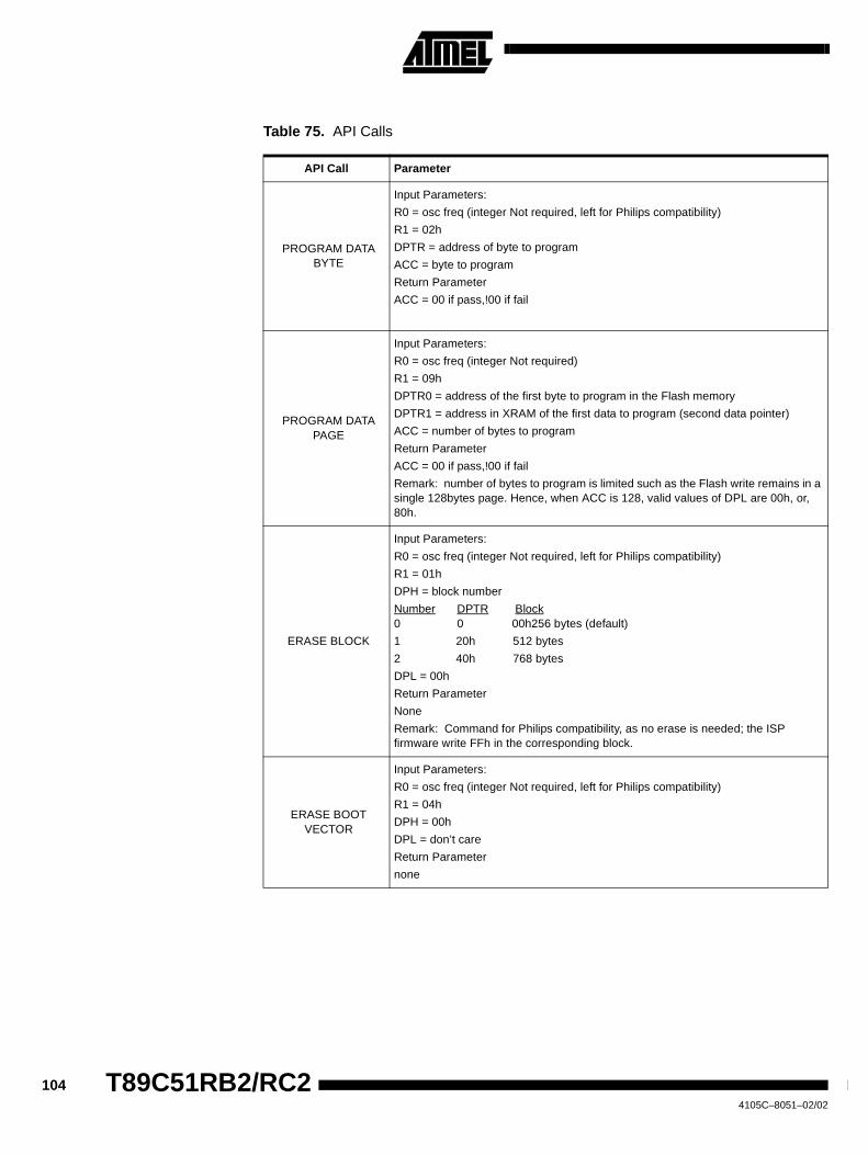
104 T89C51RB2/RC24105C–8051–02/02
Table 75. API Calls
API Call Parameter
PROGRAM DATABYTE
Input Parameters:
R0 = osc freq (integer Not required, left for Philips compatibility)
R1 = 02h
DPTR = address of byte to program
ACC = byte to program
Return Parameter
ACC = 00 if pass,!00 if fail
PROGRAM DATAPAGE
Input Parameters:
R0 = osc freq (integer Not required)
R1 = 09h
DPTR0 = address of the first byte to program in the Flash memory
DPTR1 = address in XRAM of the first data to program (second data pointer)
ACC = number of bytes to program
Return Parameter
ACC = 00 if pass,!00 if fail
Remark: number of bytes to program is limited such as the Flash write remains in asingle 128bytes page. Hence, when ACC is 128, valid values of DPL are 00h, or,80h.
ERASE BLOCK
Input Parameters:
R0 = osc freq (integer Not required, left for Philips compatibility)
R1 = 01h
DPH = block number
Number DPTR Block0 0 00h256 bytes (default)
1 20h 512 bytes
2 40h 768 bytes
DPL = 00h
Return Parameter
None
Remark: Command for Philips compatibility, as no erase is needed; the ISPfirmware write FFh in the corresponding block.
ERASE BOOTVECTOR
Input Parameters:
R0 = osc freq (integer Not required, left for Philips compatibility)
R1 = 04h
DPH = 00h
DPL = don’t care
Return Parameter
none
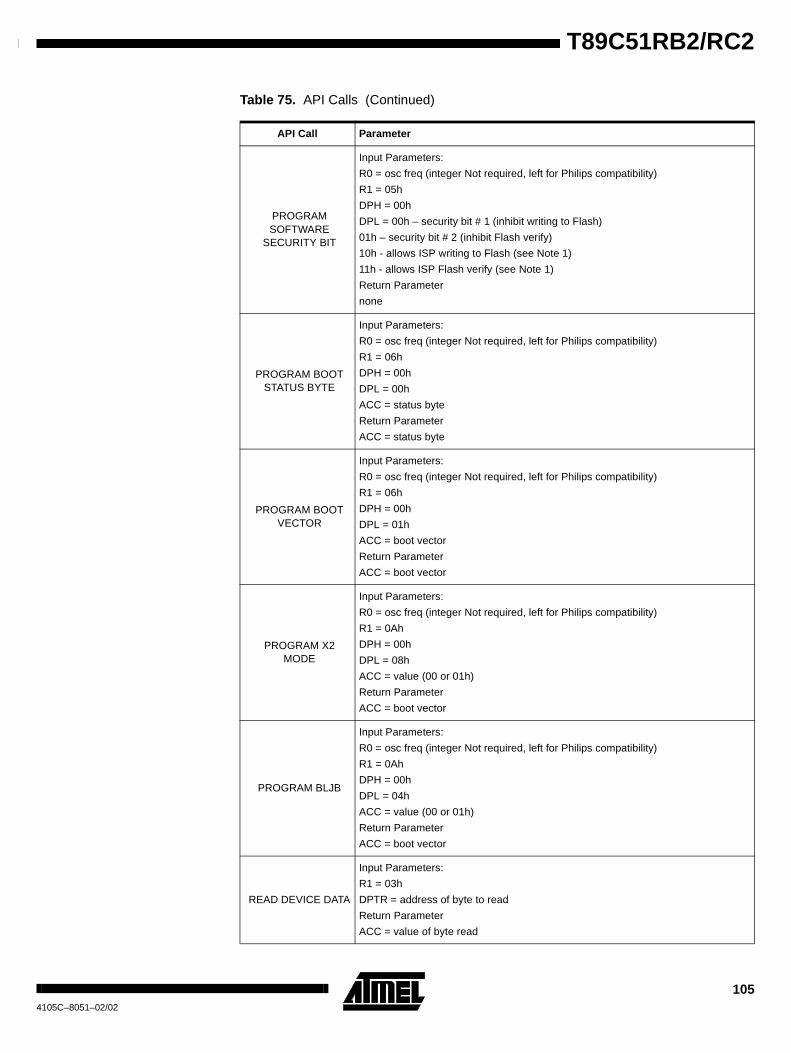
105
T89C51RB2/RC2
4105C–8051–02/02
PROGRAMSOFTWARE
SECURITY BIT
Input Parameters:
R0 = osc freq (integer Not required, left for Philips compatibility)
R1 = 05h
DPH = 00h
DPL = 00h – security bit # 1 (inhibit writing to Flash)
01h – security bit # 2 (inhibit Flash verify)
10h - allows ISP writing to Flash (see Note 1)
11h - allows ISP Flash verify (see Note 1)
Return Parameter
none
PROGRAM BOOTSTATUS BYTE
Input Parameters:
R0 = osc freq (integer Not required, left for Philips compatibility)
R1 = 06h
DPH = 00h
DPL = 00h
ACC = status byte
Return Parameter
ACC = status byte
PROGRAM BOOTVECTOR
Input Parameters:
R0 = osc freq (integer Not required, left for Philips compatibility)
R1 = 06h
DPH = 00h
DPL = 01h
ACC = boot vector
Return Parameter
ACC = boot vector
PROGRAM X2MODE
Input Parameters:
R0 = osc freq (integer Not required, left for Philips compatibility)
R1 = 0Ah
DPH = 00h
DPL = 08h
ACC = value (00 or 01h)
Return Parameter
ACC = boot vector
PROGRAM BLJB
Input Parameters:
R0 = osc freq (integer Not required, left for Philips compatibility)
R1 = 0Ah
DPH = 00h
DPL = 04h
ACC = value (00 or 01h)
Return Parameter
ACC = boot vector
READ DEVICE DATA
Input Parameters:
R1 = 03h
DPTR = address of byte to read
Return Parameter
ACC = value of byte read
Table 75. API Calls (Continued)
API Call Parameter
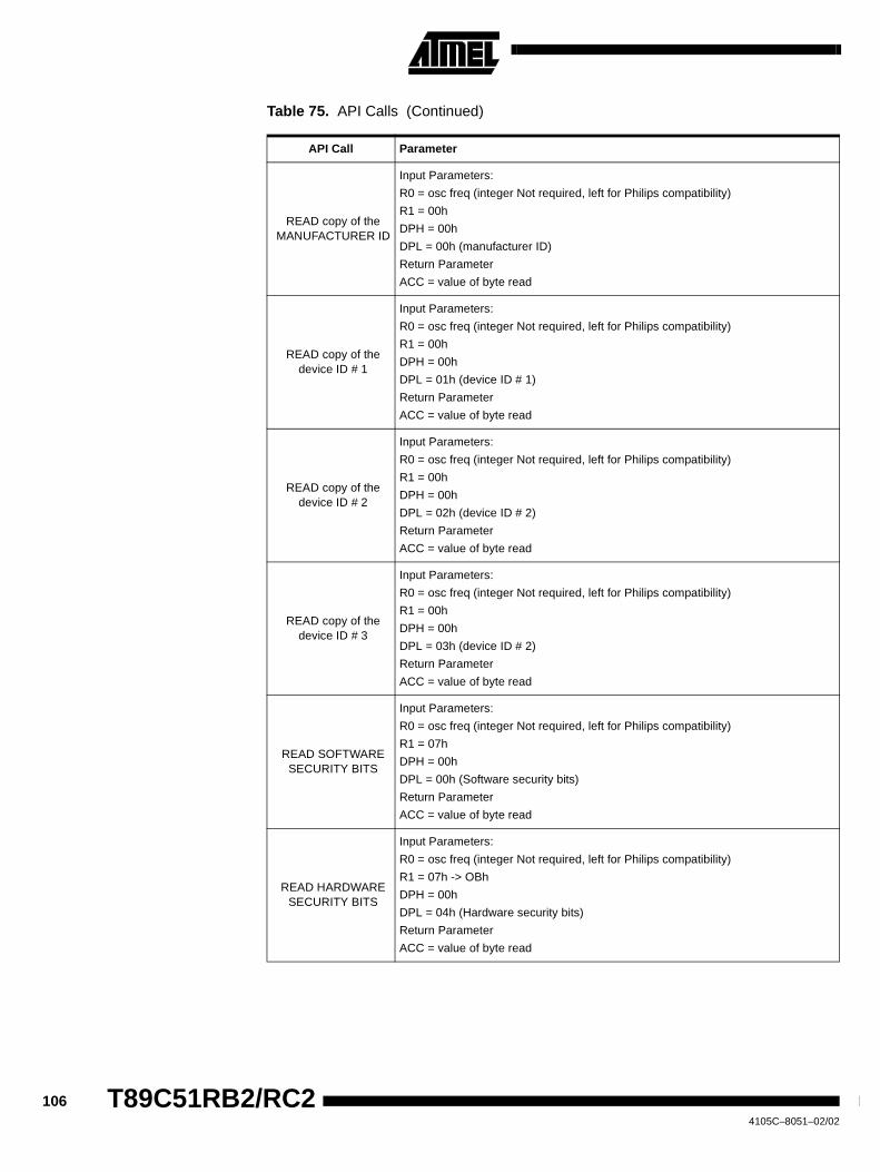
106 T89C51RB2/RC24105C–8051–02/02
READ copy of theMANUFACTURER ID
Input Parameters:
R0 = osc freq (integer Not required, left for Philips compatibility)
R1 = 00h
DPH = 00h
DPL = 00h (manufacturer ID)
Return Parameter
ACC = value of byte read
READ copy of thedevice ID # 1
Input Parameters:
R0 = osc freq (integer Not required, left for Philips compatibility)
R1 = 00h
DPH = 00h
DPL = 01h (device ID # 1)
Return Parameter
ACC = value of byte read
READ copy of thedevice ID # 2
Input Parameters:
R0 = osc freq (integer Not required, left for Philips compatibility)
R1 = 00h
DPH = 00h
DPL = 02h (device ID # 2)
Return Parameter
ACC = value of byte read
READ copy of thedevice ID # 3
Input Parameters:
R0 = osc freq (integer Not required, left for Philips compatibility)
R1 = 00h
DPH = 00h
DPL = 03h (device ID # 2)
Return Parameter
ACC = value of byte read
READ SOFTWARESECURITY BITS
Input Parameters:
R0 = osc freq (integer Not required, left for Philips compatibility)
R1 = 07h
DPH = 00h
DPL = 00h (Software security bits)
Return Parameter
ACC = value of byte read
READ HARDWARESECURITY BITS
Input Parameters:
R0 = osc freq (integer Not required, left for Philips compatibility)
R1 = 07h -> OBh
DPH = 00h
DPL = 04h (Hardware security bits)
Return Parameter
ACC = value of byte read
Table 75. API Calls (Continued)
API Call Parameter
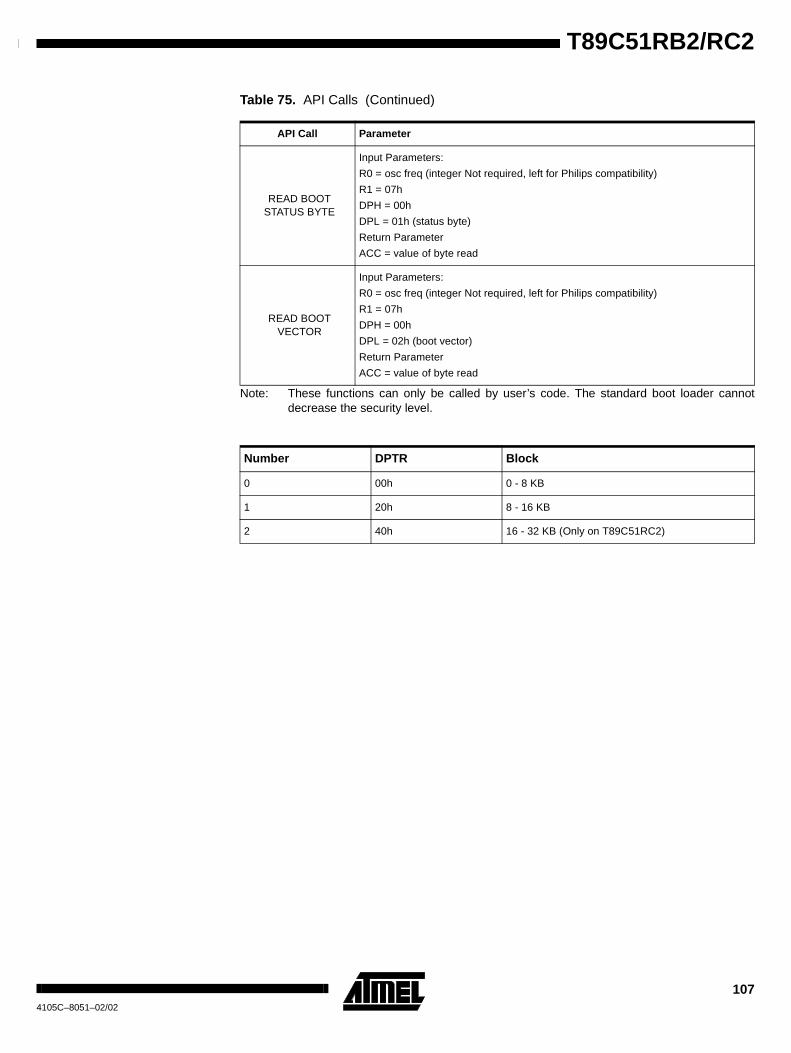
107
T89C51RB2/RC2
4105C–8051–02/02
Note: These functions can only be called by user’s code. The standard boot loader cannotdecrease the security level.
READ BOOTSTATUS BYTE
Input Parameters:
R0 = osc freq (integer Not required, left for Philips compatibility)
R1 = 07h
DPH = 00h
DPL = 01h (status byte)
Return Parameter
ACC = value of byte read
READ BOOTVECTOR
Input Parameters:
R0 = osc freq (integer Not required, left for Philips compatibility)
R1 = 07h
DPH = 00h
DPL = 02h (boot vector)
Return Parameter
ACC = value of byte read
Number DPTR Block
0 00h 0 - 8 KB
1 20h 8 - 16 KB
2 40h 16 - 32 KB (Only on T89C51RC2)
Table 75. API Calls (Continued)
API Call Parameter
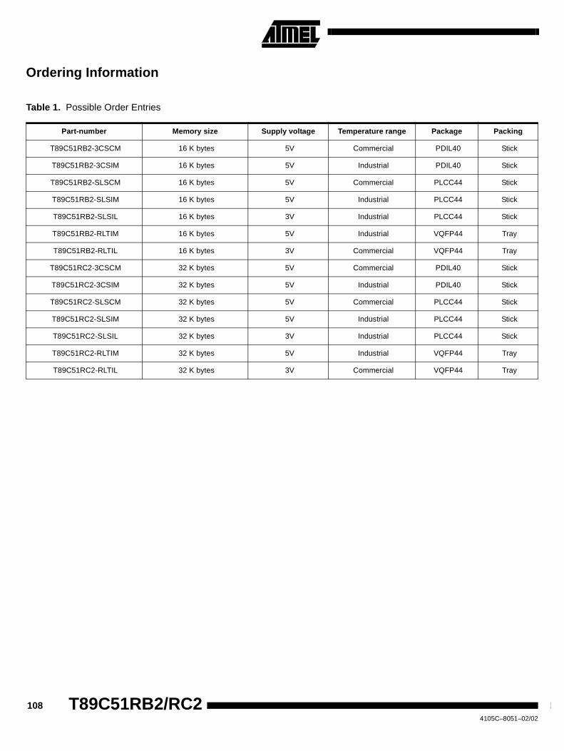
108 T89C51RB2/RC24105C–8051–02/02
Ordering Information
Table 1. Possible Order Entries
Part-number Memory size Supply voltage Temperature range Package Packing
T89C51RB2-3CSCM 16 K bytes 5V Commercial PDIL40 Stick
T89C51RB2-3CSIM 16 K bytes 5V Industrial PDIL40 Stick
T89C51RB2-SLSCM 16 K bytes 5V Commercial PLCC44 Stick
T89C51RB2-SLSIM 16 K bytes 5V Industrial PLCC44 Stick
T89C51RB2-SLSIL 16 K bytes 3V Industrial PLCC44 Stick
T89C51RB2-RLTIM 16 K bytes 5V Industrial VQFP44 Tray
T89C51RB2-RLTIL 16 K bytes 3V Commercial VQFP44 Tray
T89C51RC2-3CSCM 32 K bytes 5V Commercial PDIL40 Stick
T89C51RC2-3CSIM 32 K bytes 5V Industrial PDIL40 Stick
T89C51RC2-SLSCM 32 K bytes 5V Commercial PLCC44 Stick
T89C51RC2-SLSIM 32 K bytes 5V Industrial PLCC44 Stick
T89C51RC2-SLSIL 32 K bytes 3V Industrial PLCC44 Stick
T89C51RC2-RLTIM 32 K bytes 5V Industrial VQFP44 Tray
T89C51RC2-RLTIL 32 K bytes 3V Commercial VQFP44 Tray
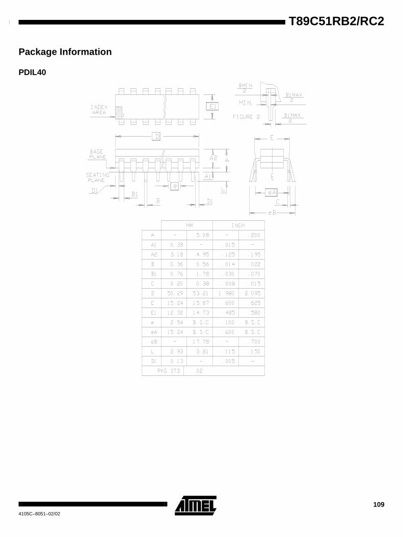
109
T89C51RB2/RC2
4105C–8051–02/02
Package Information
PDIL40
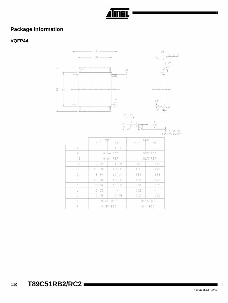
110 T89C51RB2/RC24105C–8051–02/02
Package Information
VQFP44
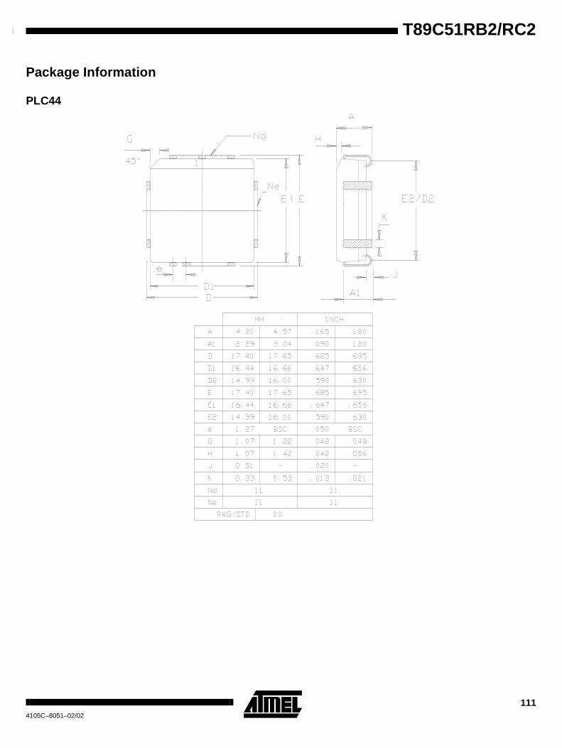
111
T89C51RB2/RC2
4105C–8051–02/02
Package Information
PLC44
i4105C–8051–01/02
Table of Contents
Features................................................................................................. 1
Description ............................................................................................ 1
Block Diagram....................................................................................... 2
SFR Mapping......................................................................................... 3
Pin Configurations................................................................................ 5
Oscillator ............................................................................................... 9Registers............................................................................................................... 9Functional Block Diagram................................................................................... 10
Enhanced Features............................................................................. 11X2 Feature .......................................................................................................... 11
Dual Data Pointer Register DPTR...................................................... 15
Expanded RAM (XRAM) ..................................................................... 18Registers............................................................................................................. 20
Timer 2 ................................................................................................. 21Auto-Reload Mode.............................................................................................. 21Programmable Clock-Output .............................................................................. 22Registers............................................................................................................. 24
Programmable Counter Array PCA................................................... 26Registers............................................................................................................. 28PCA Capture Mode............................................................................................. 3416-bit Software Timer/ Compare Mode............................................................... 35High Speed Output Mode ................................................................................... 36Pulse Width Modulator Mode.............................................................................. 37PCA Watchdog Timer ......................................................................................... 37
Serial I/O Port ...................................................................................... 39Framing Error Detection ..................................................................................... 39Automatic Address Recognition.......................................................................... 40Registers............................................................................................................. 42Baud Rate Selection for UART for Mode 1 and 3............................................... 42UART registers ................................................................................................... 45
Interrupt System ................................................................................. 50. Registers........................................................................................................... 51
ii4105C–8051–01/02
Interrupt Sources and Vector Addresses............................................................ 58
Keyboard Interface ............................................................................. 59Registers............................................................................................................. 60
Serial Port Interface (SPI)................................................................... 63Features.............................................................................................................. 63Signal Description............................................................................................... 63Functional Description ........................................................................................ 65
Hardware Watchdog Timer ................................................................ 72Using the WDT ................................................................................................... 72WDT During Power Down and Idle..................................................................... 73
ONCE™ Mode (ON Chip Emulation) .................................................. 74
Power Management ............................................................................ 75Idle Mode ............................................................................................................ 75Power-Down Mode ............................................................................................. 75
Power-off Flag..................................................................................... 77
Reduced EMI Mode............................................................................. 78
Electrical Characteristics................................................................... 79Absolute Maximum Ratings(*) ............................................................................. 79DC Parameters for Standard Voltage ................................................................. 80DC Parameters for Low Voltage ......................................................................... 81AC Parameters ................................................................................................... 83
Flash EEPROM Memory ..................................................................... 93Features.............................................................................................................. 93Flash Programming and Erasure........................................................................ 93Flash Registers and Memory Map...................................................................... 94Flash Memory Status.......................................................................................... 97Memory Organization ......................................................................................... 97Boot process....................................................................................................... 98In-System Programming (ISP).......................................................................... 100In-application Programming Method................................................................. 103
Ordering Information........................................................................ 108
Package Information ........................................................................ 109PDIL40.............................................................................................................. 109
Package Information ........................................................................ 110
iii4105C–8051–01/02
VQFP44 ............................................................................................................ 110
Package Information ........................................................................ 111PLC44............................................................................................................... 111
Table of Contents .................................................................................. i
Printed on recycled paper.
© Atmel Corporation 2002.Atmel Corporation makes no warranty for the use of its products, other than those expressly contained in the Company’s standard warrantywhich is detailed in Atmel’s Terms and Conditions located on the Company’s web site. The Company assumes no responsibility for any errorswhich may appear in this document, reserves the right to change devices or specifications detailed herein at any time without notice, and doesnot make any commitment to update the information contained herein. No licenses to patents or other intellectual property of Atmel are grantedby the Company in connection with the sale of Atmel products, expressly or by implication. Atmel’s products are not authorized for use as criticalcomponents in life support devices or systems.
Atmel Headquarters Atmel Operations
Corporate Headquarters2325 Orchard ParkwaySan Jose, CA 95131TEL 1(408) 441-0311FAX 1(408) 487-2600
EuropeAtmel SarLRoute des Arsenaux 41Casa Postale 80CH-1705 FribourgSwitzerlandTEL (41) 26-426-5555FAX (41) 26-426-5500
AsiaAtmel Asia, Ltd.Room 1219Chinachem Golden Plaza77 Mody Road TsimhatsuiEast KowloonHong KongTEL (852) 2721-9778FAX (852) 2722-1369
JapanAtmel Japan K.K.9F, Tonetsu Shinkawa Bldg.1-24-8 ShinkawaChuo-ku, Tokyo 104-0033JapanTEL (81) 3-3523-3551FAX (81) 3-3523-7581
MemoryAtmel Corporate2325 Orchard ParkwaySan Jose, CA 95131TEL 1(408) 436-4270FAX 1(408) 436-4314
MicrocontrollersAtmel Corporate2325 Orchard ParkwaySan Jose, CA 95131TEL 1(408) 436-4270FAX 1(408) 436-4314
Atmel NantesLa ChantrerieBP 7060244306 Nantes Cedex 3, FranceTEL (33) 2-40-18-18-18FAX (33) 2-40-18-19-60
ASIC/ASSP/Smart CardsAtmel RoussetZone Industrielle13106 Rousset Cedex, FranceTEL (33) 4-42-53-60-00FAX (33) 4-42-53-60-01
Atmel Colorado Springs1150 East Cheyenne Mtn. Blvd.Colorado Springs, CO 80906TEL 1(719) 576-3300FAX 1(719) 540-1759
Atmel Smart Card ICsScottish Enterprise Technology ParkMaxwell BuildingEast Kilbride G75 0QR, ScotlandTEL (44) 1355-803-000FAX (44) 1355-242-743
RF/AutomotiveAtmel HeilbronnTheresienstrasse 2Postfach 353574025 Heilbronn, GermanyTEL (49) 71-31-67-0FAX (49) 71-31-67-2340
Atmel Colorado Springs1150 East Cheyenne Mtn. Blvd.Colorado Springs, CO 80906TEL 1(719) 576-3300FAX 1(719) 540-1759
Biometrics/Imaging/Hi-Rel MPU/High Speed Converters/RF Data-com
Atmel GrenobleAvenue de RochepleineBP 12338521 Saint-Egreve Cedex, FranceTEL (33) 4-76-58-30-00FAX (33) 4-76-58-34-80
Web Sitehttp://www.atmel.com
4105C–8051–01/02 /0M
ATMEL® is a trademark of Atmel. Other terms and product names may be the trademarks of others.