CC 8-bit 256 x 8 Internal RAM Microcontroller Hardware ... · PDF file– 32-byte User...
94
Features • Compatible with MCS ® 51 Products • 20 MIPS Throughput at 20 MHz Clock Frequency and 2.4V, 85°C Operating Conditions • Single Clock Cycle per Byte Fetch • 2/4K Bytes of In-System Programmable (ISP) Flash Memory – Serial Interface for Program Downloading – 32-byte Fast Page Programming Mode – 32-byte User Signature Array • 2.4V to 5.5V V CC Operating Range • Fully Static Operation: 0 Hz to 20 MHz • 2-level Program Memory Lock • 256 x 8 Internal RAM • Hardware Multiplier • 15 Programmable I/O Lines • Configurable I/O with Quasi-bidirectional, Input, Push-pull Output, and Open-drain Modes • Enhanced UART with Automatic Address Recognition and Framing Error Detection • Enhanced SPI with Double-buffered Send/Receive • Programmable Watchdog Timer with Software Reset • 4-level Interrupt Priority • Analog Comparator with Selectable Interrupt and Debouncing • Two 16-bit Enhanced Timer/Counters with 8-bit PWM • Brown-out Detector and Power-off Flag • Internal Power-on Reset • Low Power Idle and Power-down Modes • Interrupt Recovery from Power-down Mode 1. Description The AT89LP2052/LP4052 is a low-power, high-performance CMOS 8-bit microcon- troller with 2/4K bytes of In-System Programmable Flash memory. The device is manufactured using Atmel's high-density nonvolatile memory technology and is com- patible with the industry-standard MCS-51 instruction set. The AT89LP2052/LP4052 is built around an enhanced CPU core that can fetch a single byte from memory every clock cycle. In the classic 8051 architecture, each fetch required 6 clock cycles, forc- ing instructions to execute in 12, 24 or 48 clock cycles. In the AT89LP2052/LP4052 CPU, instructions need only 1 to 4 clock cycles providing 6 to 12 times more through- put than the standard 8051. Seventy percent of instructions need only as many clock cycles as they have bytes to execute, and most of the remaining instructions require only one additional clock. The enhanced CPU core is capable of 20 MIPS throughput whereas the classic 8051 CPU can deliver only 4 MIPS at the same current consump- tion. Conversely, at the same throughput as the classic 8051, the new CPU core runs at a much lower speed and thereby greatly reduces power consumption. 8-bit Microcontroller with 2/4-Kbyte Flash AT89LP2052 AT89LP4052 3547J–MICRO–10/09
Transcript of CC 8-bit 256 x 8 Internal RAM Microcontroller Hardware ... · PDF file– 32-byte User...
8-bit Microcontroller with 2/4-Kbyte Flash
AT89LP2052AT89LP4052
3547J–MICRO–10/09
Features• Compatible with MCS®51 Products• 20 MIPS Throughput at 20 MHz Clock Frequency and 2.4V, 85°C Operating Conditions• Single Clock Cycle per Byte Fetch• 2/4K Bytes of In-System Programmable (ISP) Flash Memory
– Serial Interface for Program Downloading– 32-byte Fast Page Programming Mode– 32-byte User Signature Array
• 2.4V to 5.5V VCC Operating Range• Fully Static Operation: 0 Hz to 20 MHz• 2-level Program Memory Lock• 256 x 8 Internal RAM• Hardware Multiplier• 15 Programmable I/O Lines • Configurable I/O with Quasi-bidirectional, Input, Push-pull Output, and
Open-drain Modes• Enhanced UART with Automatic Address Recognition and Framing Error Detection• Enhanced SPI with Double-buffered Send/Receive• Programmable Watchdog Timer with Software Reset• 4-level Interrupt Priority• Analog Comparator with Selectable Interrupt and Debouncing• Two 16-bit Enhanced Timer/Counters with 8-bit PWM• Brown-out Detector and Power-off Flag• Internal Power-on Reset• Low Power Idle and Power-down Modes• Interrupt Recovery from Power-down Mode
1. DescriptionThe AT89LP2052/LP4052 is a low-power, high-performance CMOS 8-bit microcon-troller with 2/4K bytes of In-System Programmable Flash memory. The device ismanufactured using Atmel's high-density nonvolatile memory technology and is com-patible with the industry-standard MCS-51 instruction set. The AT89LP2052/LP4052is built around an enhanced CPU core that can fetch a single byte from memory everyclock cycle. In the classic 8051 architecture, each fetch required 6 clock cycles, forc-ing instructions to execute in 12, 24 or 48 clock cycles. In the AT89LP2052/LP4052CPU, instructions need only 1 to 4 clock cycles providing 6 to 12 times more through-put than the standard 8051. Seventy percent of instructions need only as many clockcycles as they have bytes to execute, and most of the remaining instructions requireonly one additional clock. The enhanced CPU core is capable of 20 MIPS throughputwhereas the classic 8051 CPU can deliver only 4 MIPS at the same current consump-tion. Conversely, at the same throughput as the classic 8051, the new CPU core runsat a much lower speed and thereby greatly reduces power consumption.
The two timer/counters in the AT89LP2052/LP4052 are enhanced with two new modes. Mode 0can be configured as a variable 9- to 16-bit timer/counter and Mode 1 can be configured as a16-bit auto-reload timer/counter. In addition both timer/counters may be configured as 8-bitPulse Width Modulators with 8-bit prescalers.
The I/O ports of the AT89LP2052/LP4052 can be independently configured in one of four oper-ating modes. In quasi-bidirectional mode, the ports operate as in the classic 8051. In inputmode, the ports are tri-stated. Push-pull output mode provides full CMOS drivers and open-drainmode provides just a pull-down.
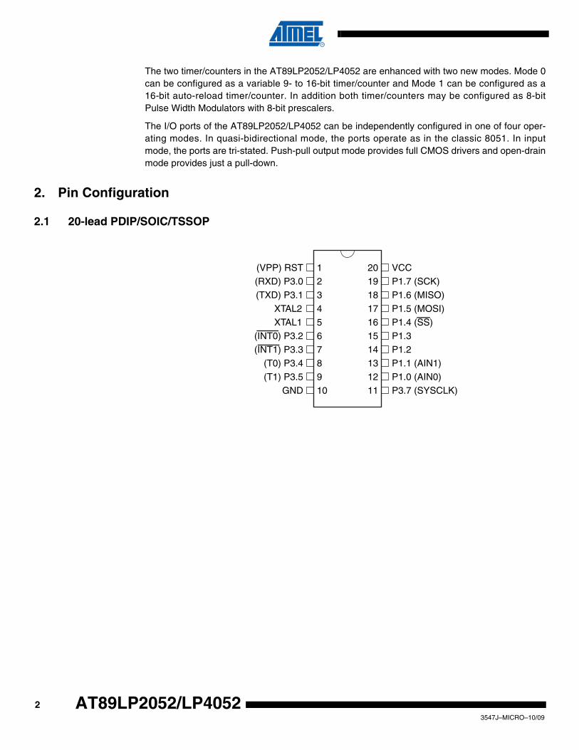
2. Pin Configuration
2.1 20-lead PDIP/SOIC/TSSOP
12345678910
20191817161514131211
(VPP) RST(RXD) P3.0(TXD) P3.1
XTAL2XTAL1
(INT0) P3.2(INT1) P3.3
(T0) P3.4(T1) P3.5
GND
VCCP1.7 (SCK)P1.6 (MISO)P1.5 (MOSI)P1.4 (SS)P1.3P1.2P1.1 (AIN1)P1.0 (AIN0)P3.7 (SYSCLK)
23547J–MICRO–10/09
AT89LP2052/LP4052
AT89LP2052/LP4052
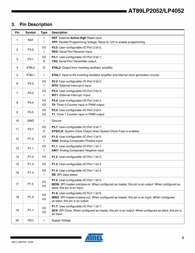
3. Pin Description
Pin Symbol Type Description
1 RSTI
I
RST: External Active-High Reset input.
VPP: Parallel Programming Voltage. Raise to 12V to enable programming.
2 P3.0I/O
I
P3.0: User-configurable I/O Port 3 bit 0.
RXD: Serial Port Receiver input.
3 P3.1I/O
O
P3.1: User-configurable I/O Port 3 bit 1.
TXD: Serial Port Transmitter output.
4 XTAL2 O XTAL2: Output from inverting oscillator amplifier.
5 XTAL1 I XTAL1: Input to the inverting oscillator amplifier and internal clock generation circuits.
6 P3.2I/O
I
P3.2: User-configurable I/O Port 3 bit 2.
INT0: External Interrupt 0 input.
7 P3.3I/O
I
P3.3: User-configurable I/O Port 3 bit 3.
INT1: External Interrupt 1input.
8 P3.4I/O
I/O
P3.4: User-configurable I/O Port 3 bit 4.
T0: Timer 0 Counter input or PWM output
9 P3.5I/O
I/O
P3.5: User-configurable I/O Port 3 bit 5.
T1: Timer 1 Counter input or PWM output
10 GND I Ground
11 P3.7I/O
O
P3.7: User-configurable I/O Port 3 bit 7.
SYSCLK: System Clock Output when System Clock Fuse is enabled.
12 P1.0I/O
I
P1.0: User-configurable I/O Port 1 bit 0.
AIN0: Analog Comparator Positive input.
13 P1.1I/O
I
P1.1: User-configurable I/O Port 1 bit 1.
AIN1: Analog Comparator Negative input.
14 P1.2 I/O P1.2: User-configurable I/O Port 1 bit 2.
15 P1.3 I/O P1.3: User-configurable I/O Port 1 bit 3
16 P1.4I/O
I
P1.4: User-configurable I/O Port 1 bit 4.
SS: SPI slave select.
17 P1.5I/OI/O
P1.5: User-configurable I/O Port 1 bit 5.
MOSI: SPI master-out/slave-in. When configured as master, this pin is an output. When configured as slave, this pin is an input.
18 P1.6I/O
I/O
P1.6: User-configurable I/O Port 1 bit 6.
MISO: SPI master-in/slave-out. When configured as master, this pin is an input. When configured as slave, this pin is an output.
19 P1.7I/OI/O
P1.7: User-configurable I/O Port 1 bit 7.
SCK: SPI Clock. When configured as master, this pin is an output. When configured as slave, this pin is an input.
20 VCC I Supply Voltage
33547J–MICRO–10/09
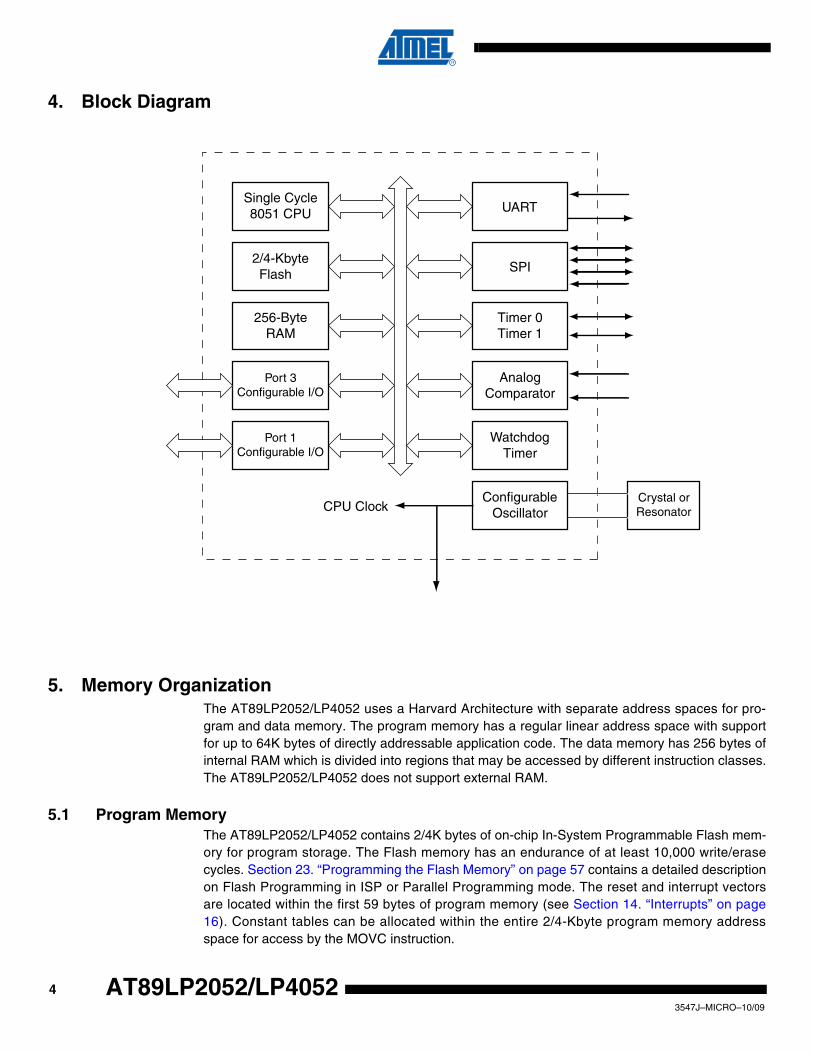
4. Block Diagram
5. Memory OrganizationThe AT89LP2052/LP4052 uses a Harvard Architecture with separate address spaces for pro-gram and data memory. The program memory has a regular linear address space with supportfor up to 64K bytes of directly addressable application code. The data memory has 256 bytes ofinternal RAM which is divided into regions that may be accessed by different instruction classes.The AT89LP2052/LP4052 does not support external RAM.
5.1 Program MemoryThe AT89LP2052/LP4052 contains 2/4K bytes of on-chip In-System Programmable Flash mem-ory for program storage. The Flash memory has an endurance of at least 10,000 write/erasecycles. Section 23. “Programming the Flash Memory” on page 57 contains a detailed descriptionon Flash Programming in ISP or Parallel Programming mode. The reset and interrupt vectorsare located within the first 59 bytes of program memory (see Section 14. “Interrupts” on page16). Constant tables can be allocated within the entire 2/4-Kbyte program memory addressspace for access by the MOVC instruction.
Single Cycle8051 CPU
2/4-KbyteFlash
256-ByteRAM
Port 3Configurable I/O
Port 1Configurable I/O
UART
SPI
Timer 0Timer 1
AnalogComparator
WatchdogTimer
ConfigurableOscillatorCPU Clock
Crystal orResonator
43547J–MICRO–10/09
AT89LP2052/LP4052
AT89LP2052/LP4052
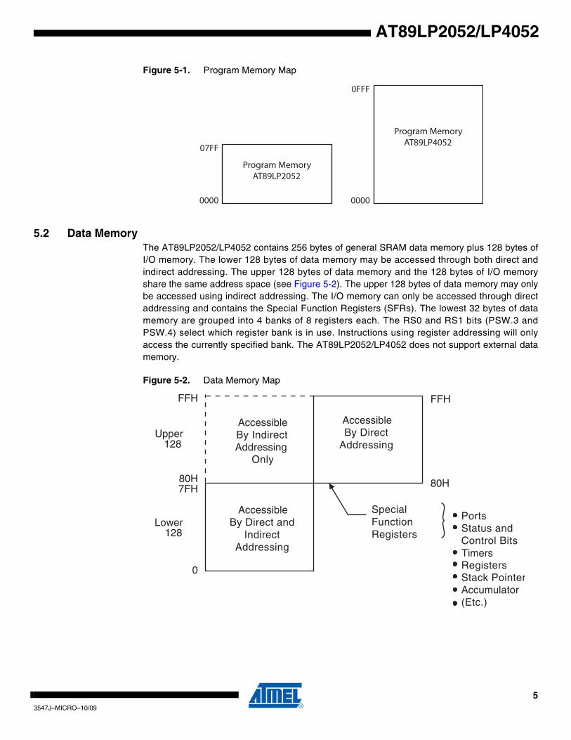
Figure 5-1. Program Memory Map
5.2 Data MemoryThe AT89LP2052/LP4052 contains 256 bytes of general SRAM data memory plus 128 bytes ofI/O memory. The lower 128 bytes of data memory may be accessed through both direct andindirect addressing. The upper 128 bytes of data memory and the 128 bytes of I/O memoryshare the same address space (see Figure 5-2). The upper 128 bytes of data memory may onlybe accessed using indirect addressing. The I/O memory can only be accessed through directaddressing and contains the Special Function Registers (SFRs). The lowest 32 bytes of datamemory are grouped into 4 banks of 8 registers each. The RS0 and RS1 bits (PSW.3 andPSW.4) select which register bank is in use. Instructions using register addressing will onlyaccess the currently specified bank. The AT89LP2052/LP4052 does not support external datamemory.
Figure 5-2. Data Memory Map
Program MemoryAT89LP2052
0000
07FF
0000
0FFF
Program MemoryAT89LP4052
FFH
Upper128
80H7FH
Lower128
0
AccessibleBy IndirectAddressing
Only
FFH
80H
SpecialFunctionRegisters
PortsStatus andControl Bits
RegistersStack PointerAccumulator(Etc.)
Timers
AccessibleBy Direct and
IndirectAddressing
AccessibleBy Direct
Addressing
53547J–MICRO–10/09
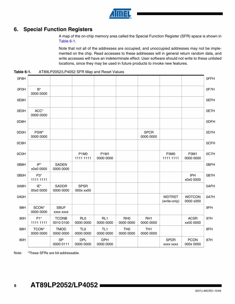
6. Special Function RegistersA map of the on-chip memory area called the Special Function Register (SFR) space is shown inTable 6-1.
Note that not all of the addresses are occupied, and unoccupied addresses may not be imple-mented on the chip. Read accesses to these addresses will in general return random data, andwrite accesses will have an indeterminate effect. User software should not write to these unlistedlocations, since they may be used in future products to invoke new features.
Note: *These SFRs are bit-addressable.
Table 6-1. AT89LP2052/LP4052 SFR Map and Reset Values
0F8H 0FFH
0F0H B*0000 0000
0F7H
0E8H 0EFH
0E0H ACC*0000 0000
0E7H
0D8H 0DFH
0D0H PSW*0000 0000
SPCR0000 0000
0D7H
0C8H 0CFH
0C0H P1M01111 1111
P1M10000 0000
P3M01111 1111
P3M10000 0000
0C7H
0B8H IP*x0x0 0000
SADEN0000 0000
0BFH
0B0H P3*1111 1111
IPHx0x0 0000
0B7H
0A8H IE*00x0 0000
SADDR0000 0000
SPSR000x xx00
0AFH
0A0H WDTRST(write-only)
WDTCON0000 x000
0A7H
98H SCON*0000 0000
SBUFxxxx xxxx
9FH
90H P1*1111 1111
TCONB0010 0100
RL00000 0000
RL10000 0000
RH00000 0000
RH10000 0000
ACSRxx00 0000
97H
88H TCON*0000 0000
TMOD0000 0000
TL00000 0000
TL10000 0000
TH00000 0000
TH10000 0000
8FH
80H SP0000 0111
DPL0000 0000
DPH0000 0000
SPDRxxxx xxxx
PCON000x 0000
87H
63547J–MICRO–10/09
AT89LP2052/LP4052
AT89LP2052/LP4052
7. Comparison to Standard 8051The AT89LP2052/LP4052 is part of a family of devices with enhanced features that are fullybinary compatible with the MCS-51 instruction set. In addition, most SFR addresses, bit assign-ments, and pin alternate functions are identical to Atmel's existing standard 8051 products.However, due to the high performance nature of the device, some system behaviors are differ-ent from those of Atmel's standard 8051 products such as AT89S52 or AT89S2051. Thedifferences from the standard 8051 are outlined in the following paragraphs.
7.1 System ClockThe CPU clock frequency equals the external XTAL1 frequency. The oscillator is no longerdivided by 2 to provide the internal clock, and x2 mode is not supported.
7.2 Instruction Execution with Single-cycle FetchThe CPU fetches one code byte from memory every clock cycle instead of every six clockcycles. This greatly increases the throughput of the CPU. As a consequence, the CPU no longerexecutes instructions in 12 to 48 clock cycles. Each instruction executes in only 1 to 4 clockcycles. See Section 22. “Instruction Set Summary” on page 52 for more details.
7.3 Interrupt HandlingThe interrupt controller polls the interrupt flags during the last clock cycle of any instruction. Inorder for an interrupt to be serviced at the end of an instruction, its flag needs to have beenlatched as active during the next to last clock cycle of the instruction, or in the last clock cycle ofthe previous instruction if the current instruction executes in only a single clock cycle.
7.4 Timer/CountersThe Timer/Counters increment at a rate of once per clock cycle. This compares to once every12 clocks in the standard 8051.
7.5 Serial PortThe baud rate of the UART in Mode 0 is 1/2 the clock frequency, compared to 1/12 the clock fre-quency in the standard 8051. In should also be noted that when using Timer 1 to generate thebaud rate in Mode 1 or Mode 3, the timer counts at the clock frequency and not at 1/12 the clockfrequency. To maintain the same baud rate in the AT89LP2052/LP4052 while running at thesame frequency as a standard 8051, the time-out period must be 12 times longer. Mode 1 ofTimer 1 supports 16-bit auto-reload to facilitate longer time-out periods for generating low baudrates.
7.6 Watchdog TimerThe Watchdog Timer in AT89LP2052/LP4052 counts at a rate of once per clock cycle. Thiscompares to once every 12 clocks in the standard 8051.
73547J–MICRO–10/09
7.7 I/O PortsThe I/O ports of the AT89LP2052/LP4052 may be configured in four different modes. On theAT89LP2052/LP4052, all the I/O ports revert to input-only (tri-stated) mode at power-up or reset.In the standard 8051, all ports are weakly pulled high during power-up or reset. To enable 8051-like ports, the ports must be put into quasi-bidirectional mode by clearing the P1M0 and P3M0SFRs.
7.8 ResetThe RST pin in the AT89LP2052/LP4052 has different pulse width requirements than the stan-dard 8051. The RST pin is sampled every clock cycle and must be held high for a minimum oftwo clock cycles, instead of 24 clock cycles, to be recognized as a valid reset pulse
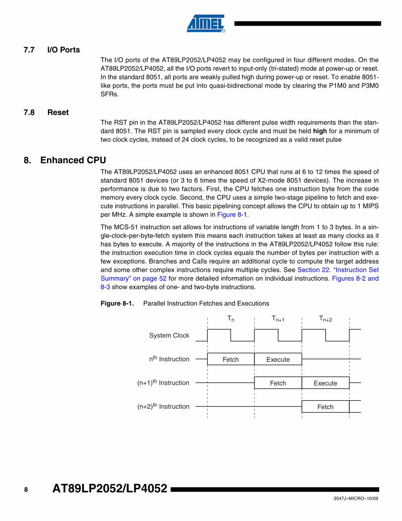
8. Enhanced CPUThe AT89LP2052/LP4052 uses an enhanced 8051 CPU that runs at 6 to 12 times the speed ofstandard 8051 devices (or 3 to 6 times the speed of X2-mode 8051 devices). The increase inperformance is due to two factors. First, the CPU fetches one instruction byte from the codememory every clock cycle. Second, the CPU uses a simple two-stage pipeline to fetch and exe-cute instructions in parallel. This basic pipelining concept allows the CPU to obtain up to 1 MIPSper MHz. A simple example is shown in Figure 8-1.
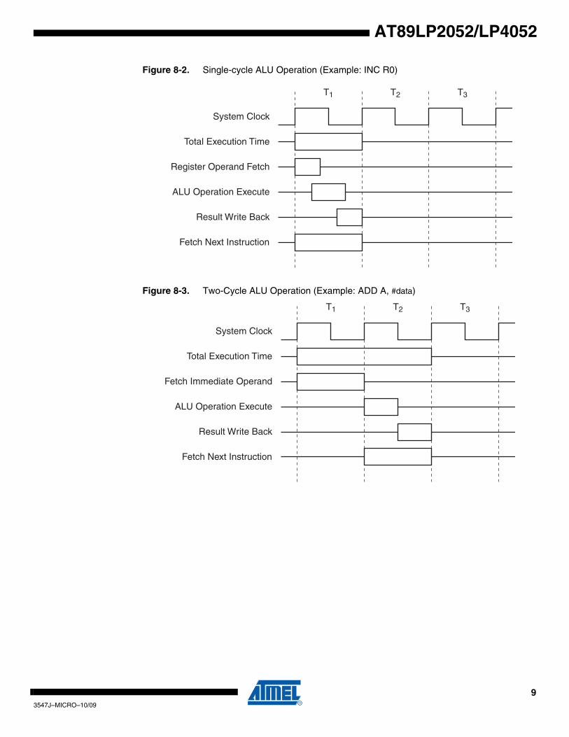
The MCS-51 instruction set allows for instructions of variable length from 1 to 3 bytes. In a sin-gle-clock-per-byte-fetch system this means each instruction takes at least as many clocks as ithas bytes to execute. A majority of the instructions in the AT89LP2052/LP4052 follow this rule:the instruction execution time in clock cycles equals the number of bytes per instruction with afew exceptions. Branches and Calls require an additional cycle to compute the target addressand some other complex instructions require multiple cycles. See Section 22. “Instruction SetSummary” on page 52 for more detailed information on individual instructions. Figures 8-2 and8-3 show examples of one- and two-byte instructions.
Figure 8-1. Parallel Instruction Fetches and Executions
System Clock
nth Instruction
(n+1)th Instruction
Fetch Execute
Fetch Execute
Fetch
Tn Tn+1 Tn+2
(n+2)th Instruction
83547J–MICRO–10/09
AT89LP2052/LP4052
AT89LP2052/LP4052
Figure 8-2. Single-cycle ALU Operation (Example: INC R0)
Figure 8-3. Two-Cycle ALU Operation (Example: ADD A, #data)
System Clock
Total Execution Time
Register Operand Fetch
T1 T2 T3
ALU Operation Execute
Result Write Back
Fetch Next Instruction
System Clock
Total Execution Time
Fetch Immediate Operand
T1 T2 T3
ALU Operation Execute
Result Write Back
Fetch Next Instruction
93547J–MICRO–10/09
9. Restrictions on Certain InstructionsThe AT89LP2052/LP4052 is an economical and cost-effective member of Atmel's growing fam-ily of microcontrollers. It contains 2/4K bytes of Flash program memory. It is fully compatible withthe MCS-51 architecture, and can be programmed using the MCS-51 instruction set. However,there are a few considerations one must keep in mind when utilizing certain instructions to pro-gram this device. All the instructions related to jumping or branching should be restricted suchthat the destination address falls within the physical program memory space of the device, whichis 2K bytes for the AT89LP2052 and 4K bytes for the AT89LP4052. This should be the responsi-bility of the software programmer. For example, LJMP 7E0H would be a valid instruction for theAT89LP2052 (with 2K bytes of memory), whereas LJMP 900H would not.
9.1 Branching InstructionsThe LCALL, LJMP, ACALL, AJMP, SJMP, and JMP @A+DPTR unconditional branching instruc-tions will execute correctly as long as the programmer keeps in mind that the destinationbranching address must fall within the physical boundaries of the program memory size (loca-tions 000H to 7FFH for the AT89LP2052, 000H to FFFH for the AT89LP4052). Violating thephysical space limits may cause unknown program behavior. With the CJNE [...], DJNZ [...], JB,JNB, JC, JNC, JBC, JZ, and JNZ conditional branching instructions, the same previous ruleapplies. Again, violating the memory boundaries may cause erratic execution. For applicationsinvolving interrupts, the normal interrupt service routine address locations of the 8051 familyarchitecture have been preserved.
9.2 MOVX-related Instructions, Data MemoryExternal DATA memory access is not supported in this device, nor is external PROGRAM mem-ory execution. Therefore, no MOVX [...] instructions should be included in the program. A typical8051 assembler will still assemble instructions, even if they are written in violation of the restric-tions mentioned above. It is the responsibility of the user to know the physical features andlimitations of the device being used and to adjust the instructions used accordingly.
10. System ClockThe system clock is generated directly from one of two selectable clock sources. The twosources are the on-chip crystal oscillator and external clock source. No internal clock division isused to generate the CPU clock from the system clock.
10.1 Crystal OscillatorWhen enabled, the internal inverting oscillator amplifier is connected between XTAL1 andXTAL2 for connection to an external quartz crystal or ceramic resonator. When using the crystaloscillator, XTAL2 should not be used to drive a board-level clock.
10.2 External Clock SourceThe external clock option is selected by setting the Oscillator Bypass fuse. This disables theamplifier and allows XTAL1 to be driven directly by the clock source. XTAL2 may be leftunconnected.
10.3 System Clock OutWhen the System Clock Out fuse is enabled, P3.7 will output the system clock with no divisionusing the push-pull output mode. During Power-down the system clock will output as “1”.
103547J–MICRO–10/09
AT89LP2052/LP4052
AT89LP2052/LP4052
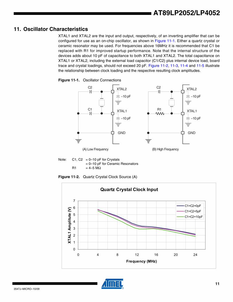
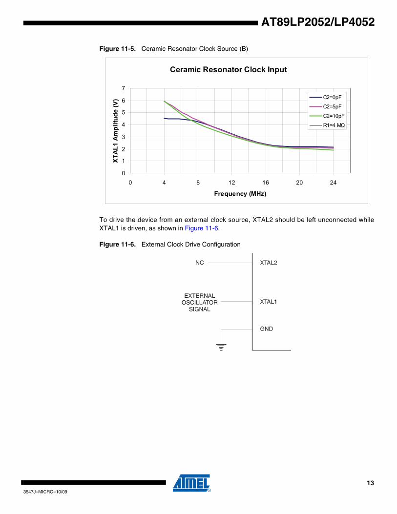
11. Oscillator Characteristics XTAL1 and XTAL2 are the input and output, respectively, of an inverting amplifier that can beconfigured for use as an on-chip oscillator, as shown in Figure 11-1. Either a quartz crystal orceramic resonator may be used. For frequencies above 16MHz it is recommended that C1 bereplaced with R1 for improved startup performance. Note that the internal structure of thedevices adds about 10 pF of capacitance to both XTAL1 and XTAL2. The total capacitance onXTAL1 or XTAL2, including the external load capacitor (C1/C2) plus internal device load, boardtrace and crystal loadings, should not exceed 20 pF. Figure 11-2, 11-3, 11-4 and 11-5 illustratethe relationship between clock loading and the respective resulting clock amplitudes.
Figure 11-1. Oscillator Connections
Note: C1, C2 = 0–10 pF for Crystals= 0–10 pF for Ceramic Resonators
R1 = 4–5 MΩ
Figure 11-2. Quartz Crystal Clock Source (A)
~10 pF
~10 pF
C2
C1
~10 pF
~10 pF
C2
R1
(A) Low Frequency (B) High Frequency
Quartz Crystal Clock Input
0
1
2
3
4
5
6
7
0 4 8 12 16 20 24
Frequency (MHz)
XTA
L1 A
mpl
itute
(V) C1=C2=0pF
C1=C2=5pF
C1=C2=10pF
113547J–MICRO–10/09
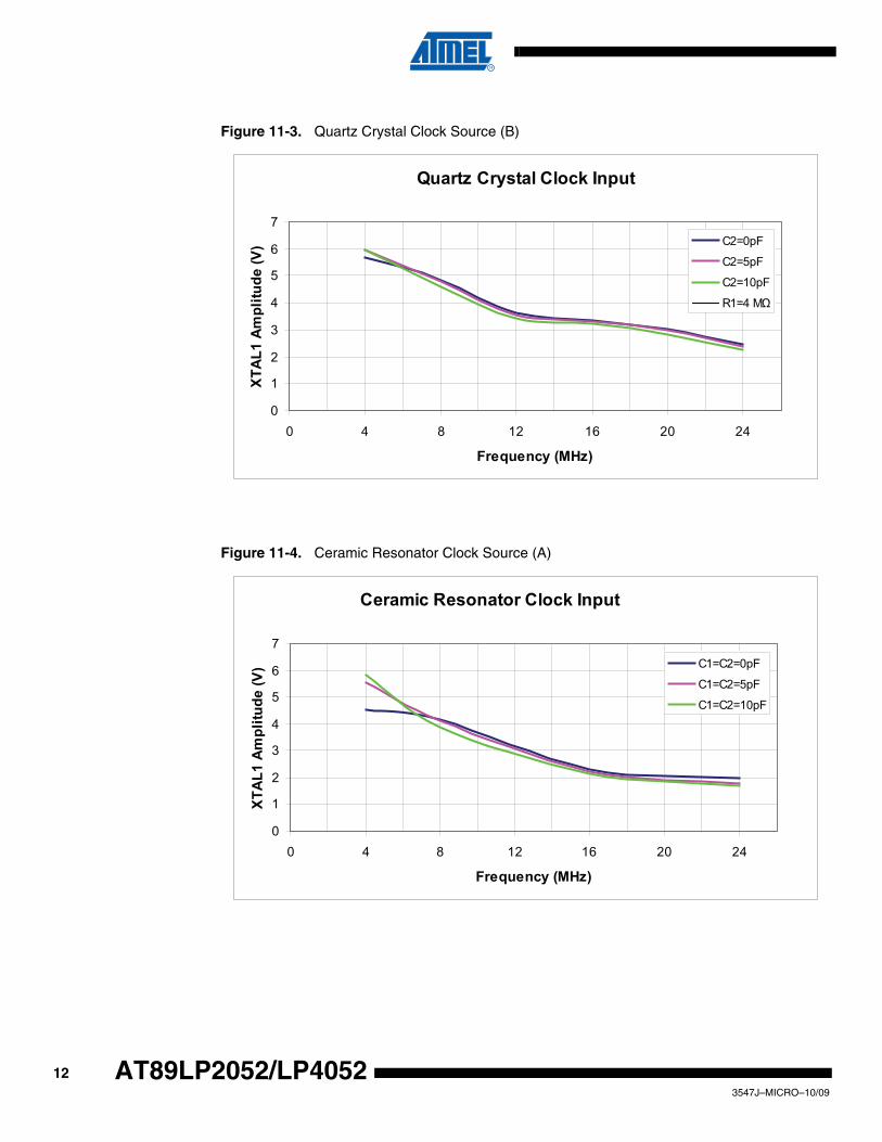
Figure 11-3. Quartz Crystal Clock Source (B)
Figure 11-4. Ceramic Resonator Clock Source (A)
Quartz Crystal Clock Input
0
1
2
3
4
5
6
7
0 4 8 12 16 20 24
Frequency (MHz)
XTA
L1 A
mpl
itude
(V) C2=0pF
C2=5pF
C2=10pF
R1=4 MΩ
Ceramic Resonator Clock Input
0
1
2
3
4
5
6
7
0 4 8 12 16 20 24
Frequency (MHz)
XTA
L1 A
mpl
itude
(V) C1=C2=0pF
C1=C2=5pF
C1=C2=10pF
123547J–MICRO–10/09
AT89LP2052/LP4052
AT89LP2052/LP4052
Figure 11-5. Ceramic Resonator Clock Source (B)
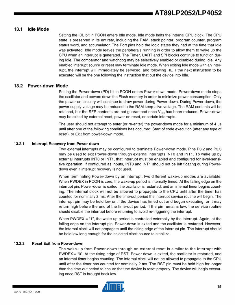
To drive the device from an external clock source, XTAL2 should be left unconnected whileXTAL1 is driven, as shown in Figure 11-6.
Figure 11-6. External Clock Drive Configuration
Ceramic Resonator Clock Input
0
1
2
3
4
5
6
7
0 4 8 12 16 20 24
Frequency (MHz)
XTA
L1 A
mpl
itude
(V) C2=0pF
C2=5pF
C2=10pF
R1=4 MΩ
133547J–MICRO–10/09
12. ResetDuring reset, all I/O Registers are set to their initial values, the port pins are tri-stated, and theprogram starts execution from the Reset Vector, 0000H. The AT89LP2052/LP4052 has foursources of reset: power-on reset, brown-out reset, external reset, and watchdog reset.
12.1 Power-on ResetA Power-on Reset (POR) is generated by an on-chip detection circuit. The detection level isnominally 1.4V. The POR is activated whenever VCC is below the detection level. The POR cir-cuit can be used to trigger the start-up reset or to detect a supply voltage failure in deviceswithout a brown-out detector. The POR circuit ensures that the device is reset from power-on.When VCC reaches the Power-on Reset threshold voltage, the POR delay counter determineshow long the device is kept in POR after VCC rise. The POR signal is activated again, withoutany delay, when VCC falls below the POR threshold level. A Power-on Reset (i.e. a cold reset)will set the POF flag in PCON.
12.2 Brown-out ResetThe AT89LP2052/LP4052 has an on-chip Brown-out Detection (BOD) circuit for monitoring theVCC level during operation by comparing it to a fixed trigger level. The trigger level for the BOD isnominally 2.2V. The purpose of the BOD is to ensure that if VCC fails or dips while executing atspeed, the system will gracefully enter reset without the possibility of errors induced by incorrectexecution. When VCC decreases to a value below the trigger level, the Brown-out Reset is imme-diately activated. When VCC increases above the trigger level, the BOD delay counter starts theMCU after the time-out period has expired.
12.3 External ResetThe RST pin functions as an active-high reset input. The pin must be held high for at least twoclock cycles to trigger the internal reset. RST also serves as the In-System Programming (ISP)enable. ISP is enabled when the external reset pin is held high and the ISP Enable fuse isenabled.
12.4 Watchdog ResetWhen the Watchdog times out, it will generate an internal reset pulse lasting 16 clock cycles.Watchdog reset will also set the WDTOVF flag in WDTCON. To prevent a Watchdog reset, thewatchdog reset sequence 1EH/E1H must be written to WDTRST before the Watchdog timesout. A Watchdog reset will occur only if the Watchdog has been enabled. The Watchdog is dis-abled by default after any reset and must always be re-enabled if needed.
13. Power Saving ModesThe AT89LP2052/LP4052 supports two different power-reducing modes: Idle and Power-down.These modes are accessed through the PCON register.
143547J–MICRO–10/09
AT89LP2052/LP4052
AT89LP2052/LP4052
13.1 Idle ModeSetting the IDL bit in PCON enters Idle mode. Idle mode halts the internal CPU clock. The CPUstate is preserved in its entirety, including the RAM, stack pointer, program counter, programstatus word, and accumulator. The Port pins hold the logic states they had at the time that Idlewas activated. Idle mode leaves the peripherals running in order to allow them to wake up theCPU when an interrupt is generated. The Timer, UART and SPI blocks continue to function dur-ing Idle. The comparator and watchdog may be selectively enabled or disabled during Idle. Anyenabled interrupt source or reset may terminate Idle mode. When exiting Idle mode with an inter-rupt, the interrupt will immediately be serviced, and following RETI the next instruction to beexecuted will be the one following the instruction that put the device into Idle.
13.2 Power-down ModeSetting the Power-down (PD) bit in PCON enters Power-down mode. Power-down mode stopsthe oscillator and powers down the Flash memory in order to minimize power consumption. Onlythe power-on circuitry will continue to draw power during Power-down. During Power-down, thepower supply voltage may be reduced to the RAM keep-alive voltage. The RAM contents will beretained, but the SFR contents are not guaranteed once VCC has been reduced. Power-downmay be exited by external reset, power-on reset, or certain interrupts.
The user should not attempt to enter (or re-enter) the power-down mode for a minimum of 4 µsuntil after one of the following conditions has occurred: Start of code execution (after any type ofreset), or Exit from power-down mode.
13.2.1 Interrupt Recovery from Power-down Two external interrupts may be configured to terminate Power-down mode. Pins P3.2 and P3.3may be used to exit Power-down through external interrupts INT0 and INT1. To wake up byexternal interrupts INT0 or INT1, that interrupt must be enabled and configured for level-sensi-tive operation. If configured as inputs, INT0 and INT1 should not be left floating during Power-down even if interrupt recovery is not used.
When terminating Power-down by an interrupt, two different wake-up modes are available.When PWDEX in PCON is zero, the wake-up period is internally timed. At the falling edge on theinterrupt pin, Power-down is exited, the oscillator is restarted, and an internal timer begins count-ing. The internal clock will not be allowed to propagate to the CPU until after the timer hascounted for nominally 2 ms. After the time-out period the interrupt service routine will begin. Theinterrupt pin may be held low until the device has timed out and begun executing, or it mayreturn high before the end of the time-out period. If the pin remains low, the service routineshould disable the interrupt before returning to avoid re-triggering the interrupt.
When PWDEX = “1”, the wake-up period is controlled externally by the interrupt. Again, at thefalling edge on the interrupt pin, Power-down is exited and the oscillator is restarted. However,the internal clock will not propagate until the rising edge of the interrupt pin. The interrupt shouldbe held low long enough for the selected clock source to stabilize.
13.2.2 Reset Exit from Power-downThe wake-up from Power-down through an external reset is similar to the interrupt withPWDEX = “0”. At the rising edge of RST, Power-down is exited, the oscillator is restarted, andan internal timer begins counting. The internal clock will not be allowed to propagate to the CPUuntil after the timer has counted for nominally 2 ms. The RST pin must be held high for longerthan the time-out period to ensure that the device is reset properly. The device will begin execut-ing once RST is brought back low.
153547J–MICRO–10/09
14. InterruptsThe AT89LP2052/LP4052 provides 6 interrupt sources: two external interrupts, two timer inter-rupts, a serial port interrupt, and an analog comparator interrupt. These interrupts and thesystem reset each have a separate program vector at the start of the program memory space.Each interrupt source can be individually enabled or disabled by setting or clearing a bit in theinterrupt enable register IE. The IE register also contains a global disable bit, EA, which disablesall interrupts.
Each interrupt source can be individually programmed to one of four priority levels by setting orclearing bits in the interrupt priority registers IP and IPH. An interrupt service routine in progresscan be interrupted by a higher priority interrupt, but not by another interrupt of the same or lowerpriority. The highest priority interrupt cannot be interrupted by any other interrupt source. If tworequests of different priority levels are pending at the end of an instruction, the request of higherpriority level is serviced. If requests of the same priority level are pending at the end of aninstruction, an internal polling sequence determines which request is serviced. The pollingsequence is based on the vector address; an interrupt with a lower vector address has higherpriority than an interrupt with a higher vector address. Note that the polling sequence is onlyused to resolve pending requests of the same priority level.
The External Interrupts INT0 and INT1 can each be either level-activated or edge-activated,depending on bits IT0 and IT1 in Register TCON. The flags that actually generate these inter-rupts are the IE0 and IE1 bits in TCON. When the service routine is vectored to, hardware clearsthe flag that generated an external interrupt only if the interrupt was edge-activated. If the inter-rupt was level activated, then the external requesting source (rather than the on-chip hardware)controls the request flag.
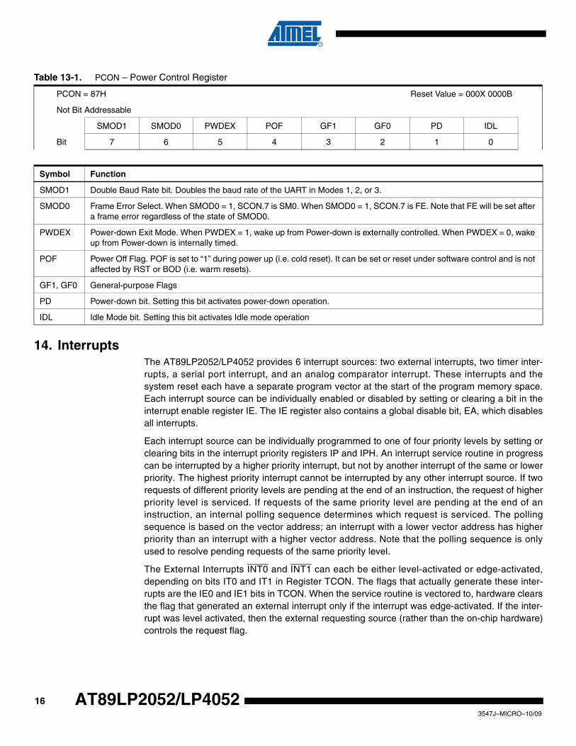
Table 13-1. PCON – Power Control Register
PCON = 87H Reset Value = 000X 0000B
Not Bit Addressable
SMOD1 SMOD0 PWDEX POF GF1 GF0 PD IDL
Bit 7 6 5 4 3 2 1 0
Symbol Function
SMOD1 Double Baud Rate bit. Doubles the baud rate of the UART in Modes 1, 2, or 3.
SMOD0 Frame Error Select. When SMOD0 = 1, SCON.7 is SM0. When SMOD0 = 1, SCON.7 is FE. Note that FE will be set after a frame error regardless of the state of SMOD0.
PWDEX Power-down Exit Mode. When PWDEX = 1, wake up from Power-down is externally controlled. When PWDEX = 0, wake up from Power-down is internally timed.
POF Power Off Flag. POF is set to “1” during power up (i.e. cold reset). It can be set or reset under software control and is not affected by RST or BOD (i.e. warm resets).
GF1, GF0 General-purpose Flags
PD Power-down bit. Setting this bit activates power-down operation.
IDL Idle Mode bit. Setting this bit activates Idle mode operation
163547J–MICRO–10/09
AT89LP2052/LP4052
AT89LP2052/LP4052
The Timer 0 and Timer 1 Interrupts are generated by TF0 and TF1, which are set by a rollover intheir respective Timer/Counter registers (except for Timer 0 in Mode 3). When a timer interrupt isgenerated, the on-chip hardware clears the flag that generated it when the service routine isvectored to.
The Serial Port Interrupt is generated by the logic OR of RI and TI in SCON plus SPIF in SPSR.None of these flags is cleared by hardware when the service routine is vectored to. In fact, theservice routine normally must determine whether RI, TI, or SPIF generated the interrupt, and thebit must be cleared by software.
The CF bit in ACSR generates the Comparator Interrupt. The flag is not cleared by hardwarewhen the service routine is vectored to and must be cleared by software.
Most of the bits that generate interrupts can be set or cleared by software, with the same resultas though they had been set or cleared by hardware. That is, interrupts can be generated andpending interrupts can be canceled in software. The exception is the SPI interrupt flag SPIF.This flag is only set by hardware and may only be cleared by software.
14.1 Interrupt Response TimeThe interrupt flags may be set by their hardware in any clock cycle. The interrupt controller pollsthe flags in the last clock cycle of the instruction in progress. If one of the flags was set in thepreceding cycle, the polling cycle will find it and the interrupt system will generate an LCALL tothe appropriate service routine as the next instruction, provided that the interrupt is not blockedby any of the following conditions: an interrupt of equal or higher priority level is already in prog-ress; the instruction in progress is RETI or any write to the IE, IP, or IPH registers. Either ofthese conditions will block the generation of the LCALL to the interrupt service routine. The sec-ond condition ensures that if the instruction in progress is RETI or any access to IE, IP or IPH,then at least one more instruction will be executed before any interrupt is vectored to. The poll-ing cycle is repeated at the last cycle of each instruction, and the values polled are the valuesthat were present at the previous clock cycle. If an active interrupt flag is not being servicedbecause of one of the above conditions and is no longer active when the blocking condition isremoved, the denied interrupt will not be serviced. In other words, the fact that the interrupt flagwas once active but not serviced is not remembered. Every polling cycle is new.
Table 14-1. Interrupt Vector Addresses
Interrupt Source Vector Address
System Reset RST or POR or BOD 0000H
External Interrupt 0 IE0 0003H
Timer 0 Overflow TF0 000BH
External Interrupt 1 IE1 0013H
Timer 1 Overflow TF1 001BH
Serial Port RI or TI or SPIF 0023H
Reserved – 002BH
Analog Comparator CF 0033H
173547J–MICRO–10/09
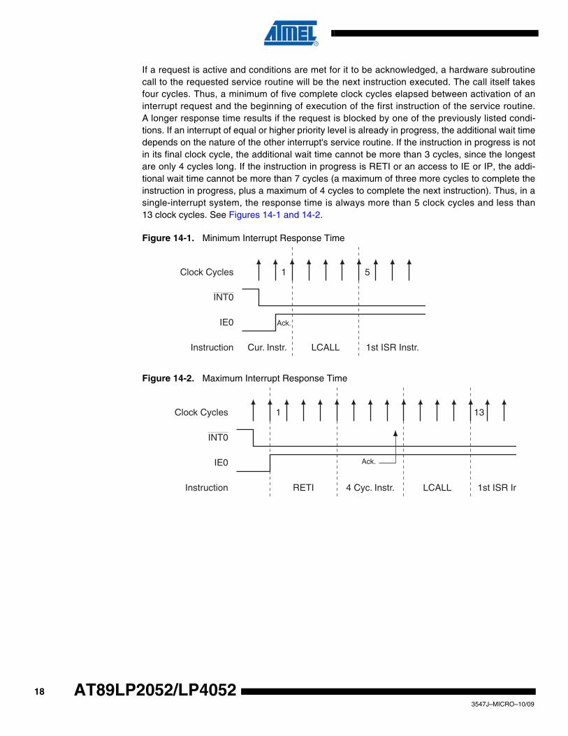
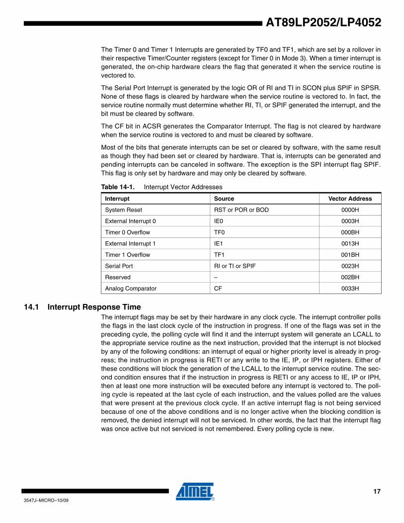
If a request is active and conditions are met for it to be acknowledged, a hardware subroutinecall to the requested service routine will be the next instruction executed. The call itself takesfour cycles. Thus, a minimum of five complete clock cycles elapsed between activation of aninterrupt request and the beginning of execution of the first instruction of the service routine.A longer response time results if the request is blocked by one of the previously listed condi-tions. If an interrupt of equal or higher priority level is already in progress, the additional wait timedepends on the nature of the other interrupt's service routine. If the instruction in progress is notin its final clock cycle, the additional wait time cannot be more than 3 cycles, since the longestare only 4 cycles long. If the instruction in progress is RETI or an access to IE or IP, the addi-tional wait time cannot be more than 7 cycles (a maximum of three more cycles to complete theinstruction in progress, plus a maximum of 4 cycles to complete the next instruction). Thus, in asingle-interrupt system, the response time is always more than 5 clock cycles and less than13 clock cycles. See Figures 14-1 and 14-2.
Figure 14-1. Minimum Interrupt Response Time
Figure 14-2. Maximum Interrupt Response Time
Clock Cycles
INT0
IE0
1 5
Instruction LCALL 1st ISR Instr.Cur. Instr.
Ack.
Clock Cycles
INT0
IE0
1 13
Instruction RETI 4 Cyc. Instr. LCALL 1st ISR In
Ack.
183547J–MICRO–10/09
AT89LP2052/LP4052
AT89LP2052/LP4052
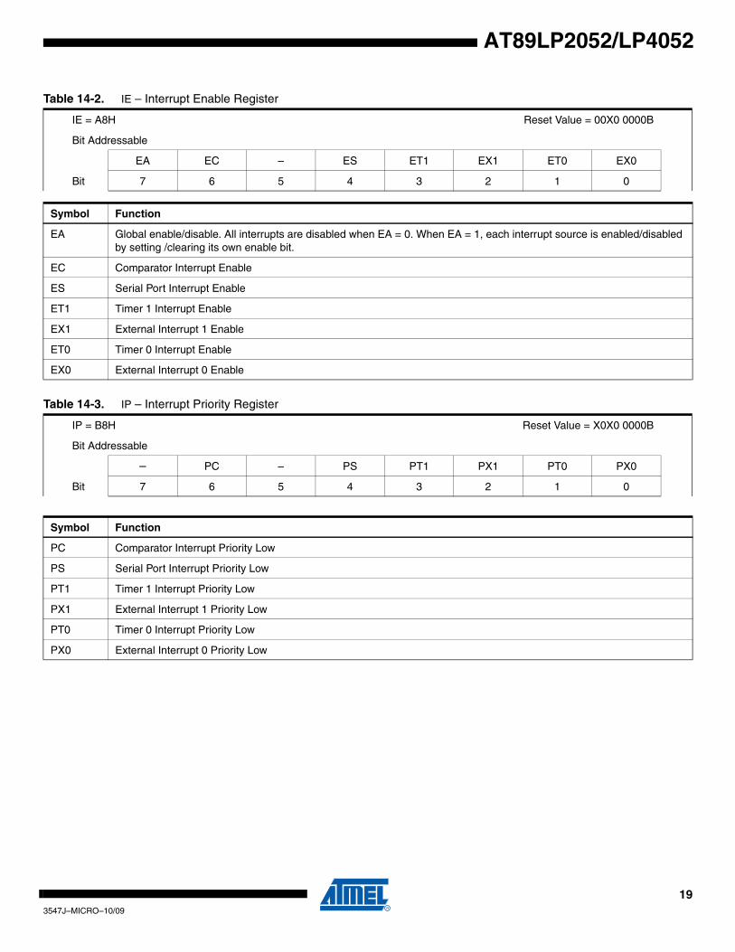
Table 14-2. IE – Interrupt Enable Register
IE = A8H Reset Value = 00X0 0000B
Bit Addressable
EA EC – ES ET1 EX1 ET0 EX0
Bit 7 6 5 4 3 2 1 0
Symbol Function
EA Global enable/disable. All interrupts are disabled when EA = 0. When EA = 1, each interrupt source is enabled/disabled by setting /clearing its own enable bit.
EC Comparator Interrupt Enable
ES Serial Port Interrupt Enable
ET1 Timer 1 Interrupt Enable
EX1 External Interrupt 1 Enable
ET0 Timer 0 Interrupt Enable
EX0 External Interrupt 0 Enable
Table 14-3. IP – Interrupt Priority Register
IP = B8H Reset Value = X0X0 0000B
Bit Addressable
– PC – PS PT1 PX1 PT0 PX0
Bit 7 6 5 4 3 2 1 0
Symbol Function
PC Comparator Interrupt Priority Low
PS Serial Port Interrupt Priority Low
PT1 Timer 1 Interrupt Priority Low
PX1 External Interrupt 1 Priority Low
PT0 Timer 0 Interrupt Priority Low
PX0 External Interrupt 0 Priority Low
193547J–MICRO–10/09
15. I/O PortsAll 15 port pins on the AT89LP2052/LP4052 may be configured to one of four modes: quasi-bidi-rectional (standard 8051 port outputs), push-pull output, open-drain output, or input-only. Portmodes may be assigned in software on a pin-by-pin basis as shown in Table 15-1. All port pinsdefault to input-only mode after reset. Each port pin also has a Schmitt-triggered input forimproved input noise rejection. During Power-down all the Schmitt-triggered inputs are disabledwith the exception of P3.2 and P3.3, which may be used to wake-up the device. Therefore P3.2and P3.3 should not be left floating during Power-down.
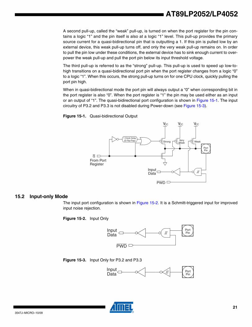
15.1 Quasi-bidirectional OutputPort pins in quasi-bidirectional output mode function similar to standard 8051 port pins. A Quasi-bidirectional port can be used both as an input and output without the need to reconfigure theport. This is possible because when the port outputs a logic high, it is weakly driven, allowing anexternal device to pull the pin low. When the pin is driven low, it is driven strongly and able tosink a large current. There are three pull-up transistors in the quasi-bidirectional output thatserve different purposes.
One of these pull-ups, called the “very weak” pull-up, is turned on whenever the port register forthe pin contains a logic “1”. This very weak pull-up sources a very small current that will pull thepin high if it is left floating.
Table 14-4. IPH – Interrupt Priority High Register
IPH = B7H Reset Value = X0X0 0000B
Not Bit Addressable
– PCH – PSH PT1H PX1H PT0H PX0H
Bit 7 6 5 4 3 2 1 0
Symbol Function
PCH Comparator Interrupt Priority High
PSH Serial Port Interrupt Priority High
PT1H Timer 1 Interrupt Priority High
PX1H External Interrupt 1 Priority High
PT0H Timer 0 Interrupt Priority High
PX0H External Interrupt 0 Priority High
Table 15-1. Configuration Modes for Port x, Bit y
PxM0.y PxM1.y Port Mode
0 0 Quasi-bidirectional
0 1 Push-pull Output
1 0 Input Only (High Impedance)
1 1 Open-Drain Output
203547J–MICRO–10/09
AT89LP2052/LP4052
AT89LP2052/LP4052
A second pull-up, called the “weak” pull-up, is turned on when the port register for the pin con-tains a logic “1” and the pin itself is also at a logic “1” level. This pull-up provides the primarysource current for a quasi-bidirectional pin that is outputting a 1. If this pin is pulled low by anexternal device, this weak pull-up turns off, and only the very weak pull-up remains on. In orderto pull the pin low under these conditions, the external device has to sink enough current to over-power the weak pull-up and pull the port pin below its input threshold voltage.
The third pull-up is referred to as the “strong” pull-up. This pull-up is used to speed up low-to-high transitions on a quasi-bidirectional port pin when the port register changes from a logic “0”to a logic “1”. When this occurs, the strong pull-up turns on for one CPU clock, quickly pulling theport pin high.
When in quasi-bidirectional mode the port pin will always output a “0” when corresponding bit inthe port register is also “0”. When the port register is “1” the pin may be used either as an inputor an output of “1”. The quasi-bidirectional port configuration is shown in Figure 15-1. The inputcircuitry of P3.2 and P3.3 is not disabled during Power-down (see Figure 15-3).
Figure 15-1. Quasi-bidirectional Output
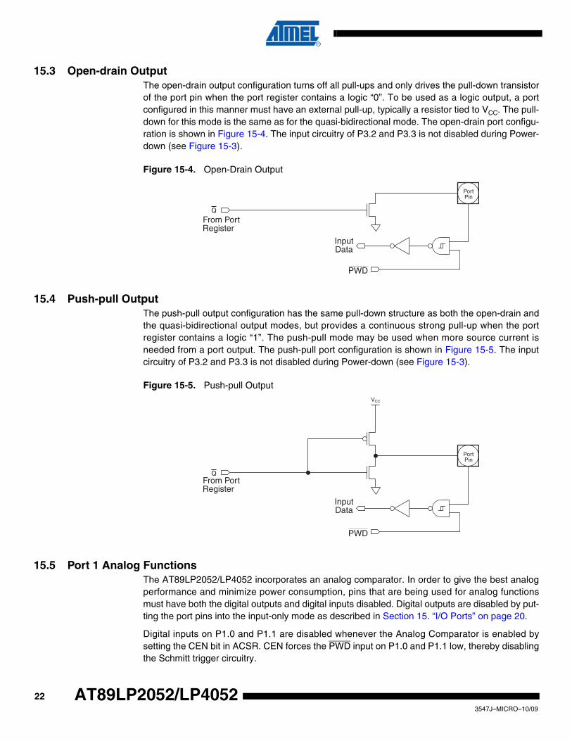
15.2 Input-only ModeThe input port configuration is shown in Figure 15-2. It is a Schmitt-triggered input for improvedinput noise rejection.
Figure 15-2. Input Only
Figure 15-3. Input Only for P3.2 and P3.3
1 Clock Delay(D Flip-Flop) Strong Very
Weak Weak
PortPin
VCC VCC VCC
From PortRegister
InputData
PWD
PortPin
InputData
PWD
PortPin
InputData
213547J–MICRO–10/09
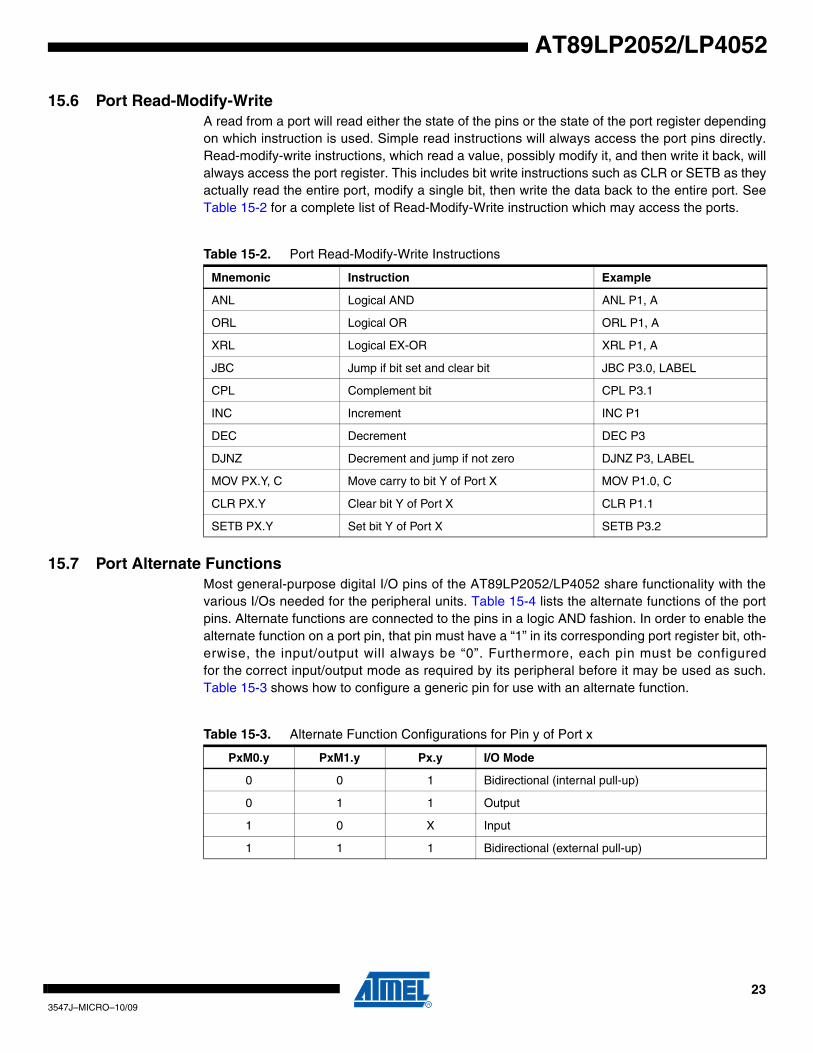
15.3 Open-drain OutputThe open-drain output configuration turns off all pull-ups and only drives the pull-down transistorof the port pin when the port register contains a logic “0”. To be used as a logic output, a portconfigured in this manner must have an external pull-up, typically a resistor tied to VCC. The pull-down for this mode is the same as for the quasi-bidirectional mode. The open-drain port configu-ration is shown in Figure 15-4. The input circuitry of P3.2 and P3.3 is not disabled during Power-down (see Figure 15-3).
Figure 15-4. Open-Drain Output
15.4 Push-pull OutputThe push-pull output configuration has the same pull-down structure as both the open-drain andthe quasi-bidirectional output modes, but provides a continuous strong pull-up when the portregister contains a logic “1”. The push-pull mode may be used when more source current isneeded from a port output. The push-pull port configuration is shown in Figure 15-5. The inputcircuitry of P3.2 and P3.3 is not disabled during Power-down (see Figure 15-3).
Figure 15-5. Push-pull Output
15.5 Port 1 Analog FunctionsThe AT89LP2052/LP4052 incorporates an analog comparator. In order to give the best analogperformance and minimize power consumption, pins that are being used for analog functionsmust have both the digital outputs and digital inputs disabled. Digital outputs are disabled by put-ting the port pins into the input-only mode as described in Section 15. “I/O Ports” on page 20.
Digital inputs on P1.0 and P1.1 are disabled whenever the Analog Comparator is enabled bysetting the CEN bit in ACSR. CEN forces the PWD input on P1.0 and P1.1 low, thereby disablingthe Schmitt trigger circuitry.
PortPin
From PortRegister
InputData
PWD
PortPin
VCC
From PortRegister
InputData
PWD
223547J–MICRO–10/09
AT89LP2052/LP4052
AT89LP2052/LP4052
15.6 Port Read-Modify-Write A read from a port will read either the state of the pins or the state of the port register dependingon which instruction is used. Simple read instructions will always access the port pins directly.Read-modify-write instructions, which read a value, possibly modify it, and then write it back, willalways access the port register. This includes bit write instructions such as CLR or SETB as theyactually read the entire port, modify a single bit, then write the data back to the entire port. SeeTable 15-2 for a complete list of Read-Modify-Write instruction which may access the ports.
15.7 Port Alternate FunctionsMost general-purpose digital I/O pins of the AT89LP2052/LP4052 share functionality with thevarious I/Os needed for the peripheral units. Table 15-4 lists the alternate functions of the portpins. Alternate functions are connected to the pins in a logic AND fashion. In order to enable thealternate function on a port pin, that pin must have a “1” in its corresponding port register bit, oth-erwise, the input/output will always be “0”. Furthermore, each pin must be configuredfor the correct input/output mode as required by its peripheral before it may be used as such.Table 15-3 shows how to configure a generic pin for use with an alternate function.
Table 15-2. Port Read-Modify-Write Instructions
Mnemonic Instruction Example
ANL Logical AND ANL P1, A
ORL Logical OR ORL P1, A
XRL Logical EX-OR XRL P1, A
JBC Jump if bit set and clear bit JBC P3.0, LABEL
CPL Complement bit CPL P3.1
INC Increment INC P1
DEC Decrement DEC P3
DJNZ Decrement and jump if not zero DJNZ P3, LABEL
MOV PX.Y, C Move carry to bit Y of Port X MOV P1.0, C
CLR PX.Y Clear bit Y of Port X CLR P1.1
SETB PX.Y Set bit Y of Port X SETB P3.2
Table 15-3. Alternate Function Configurations for Pin y of Port x
PxM0.y PxM1.y Px.y I/O Mode
0 0 1 Bidirectional (internal pull-up)
0 1 1 Output
1 0 X Input
1 1 1 Bidirectional (external pull-up)
233547J–MICRO–10/09
16. Enhanced Timer/CountersThe AT89LP2052/LP4052 has two 16-bit Timer/Counter registers: Timer 0 and Timer 1. As aTimer, the register is incremented every clock cycle. Thus, the register counts clock cycles.Since a clock cycle consists of one oscillator period, the count rate is equal to the oscillatorfrequency.
As a Counter, the register is incremented in response to a 1-to-0 transition at its correspondinginput pin, T0 or T1. The external input is sampled every clock cycle. When the samples show ahigh in one cycle and a low in the next cycle, the count is incremented. The new count valueappears in the register during the cycle following the one in which the transition was detected.Since 2 clock cycles are required to recognize a 1-to-0 transition, the maximum count rate is 1/2of the oscillator frequency. There are no restrictions on the duty cycle of the input signal, but itshould be held for at least one full clock cycle to ensure that a given level is sampled at leastonce before it changes.
Furthermore, the Timer or Counter functions for Timer 0 and Timer 1 have four operating modes:variable width timer/counter, 16 bit auto-reload timer/counter, 8 bit auto-reload timer/counter,and split timer/counter. The control bits C/T in the Special Function Register TMOD select theTimer or Counter function. The bit pairs (M1, M0) in TMOD select the operating modes.
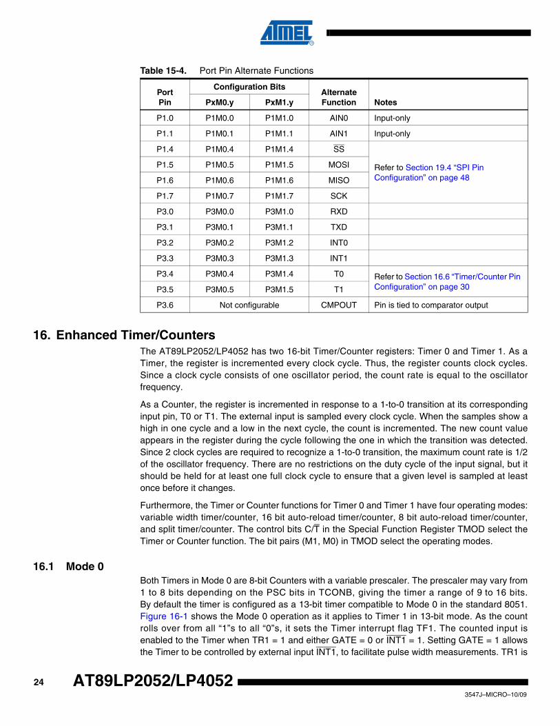
16.1 Mode 0Both Timers in Mode 0 are 8-bit Counters with a variable prescaler. The prescaler may vary from1 to 8 bits depending on the PSC bits in TCONB, giving the timer a range of 9 to 16 bits.By default the timer is configured as a 13-bit timer compatible to Mode 0 in the standard 8051.Figure 16-1 shows the Mode 0 operation as it applies to Timer 1 in 13-bit mode. As the countrolls over from all “1”s to all “0”s, it sets the Timer interrupt flag TF1. The counted input isenabled to the Timer when TR1 = 1 and either GATE = 0 or INT1 = 1. Setting GATE = 1 allowsthe Timer to be controlled by external input INT1, to facilitate pulse width measurements. TR1 is
Table 15-4. Port Pin Alternate Functions
PortPin
Configuration BitsAlternateFunction NotesPxM0.y PxM1.y
P1.0 P1M0.0 P1M1.0 AIN0 Input-only
P1.1 P1M0.1 P1M1.1 AIN1 Input-only
P1.4 P1M0.4 P1M1.4 SS
Refer to Section 19.4 “SPI Pin Configuration” on page 48
P1.5 P1M0.5 P1M1.5 MOSI
P1.6 P1M0.6 P1M1.6 MISO
P1.7 P1M0.7 P1M1.7 SCK
P3.0 P3M0.0 P3M1.0 RXD
P3.1 P3M0.1 P3M1.1 TXD
P3.2 P3M0.2 P3M1.2 INT0
P3.3 P3M0.3 P3M1.3 INT1
P3.4 P3M0.4 P3M1.4 T0 Refer to Section 16.6 “Timer/Counter Pin Configuration” on page 30P3.5 P3M0.5 P3M1.5 T1
P3.6 Not configurable CMPOUT Pin is tied to comparator output
243547J–MICRO–10/09
AT89LP2052/LP4052
AT89LP2052/LP4052
a control bit in the Special Function Register TCON. GATE is in TMOD. The 13-bit register con-sists of all 8 bits of TH1 and the lower 5 bits of TL1. The upper 3 bits of TL1 are indeterminateand should be ignored. Setting the run flag (TR1) does not clear the registers. See Figure 16-1.
Figure 16-1. Timer/Counter 1 Mode 0: Variable Width Counter
Mode 0 operation is the same for Timer 0 as for Timer 1, except that TR0, TF0 and INT0 replacethe corresponding Timer 1 signals in Figure 16-1. There are two different GATE bits, one forTimer 1 (TMOD.7) and one for Timer 0 (TMOD.3).
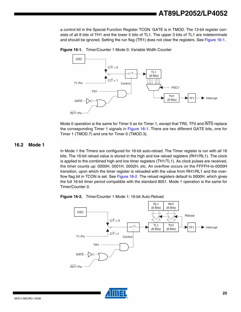
16.2 Mode 1In Mode 1 the Timers are configured for 16-bit auto-reload. The Timer register is run with all 16bits. The 16-bit reload value is stored in the high and low reload registers (RH1/RL1). The clockis applied to the combined high and low timer registers (TH1/TL1). As clock pulses are received,the timer counts up: 0000H, 0001H, 0002H, etc. An overflow occurs on the FFFFH-to-0000Htransition, upon which the timer register is reloaded with the value from RH1/RL1 and the over-flow flag bit in TCON is set. See Figure 16-2. The reload registers default to 0000H, which givesthe full 16-bit timer period compatible with the standard 8051. Mode 1 operation is the same forTimer/Counter 0.
Figure 16-2. Timer/Counter 1 Mode 1: 16-bit Auto-Reload
OSC
T1 Pin
TR1
GATE
INT1 Pin
TL1(8 Bits)
Control
Interrupt
C/T = 0
C/T = 1
PSC1
TH1(8 Bits) TF1
OSC
T1 Pin
TR1
GATE
INT1 Pin
TL1(8 Bits)
Control
Interrupt
C/T = 0
C/T =1
TH1(8 Bits) TF1
RL1(8 Bits)
RH1(8 Bits)
Reload
253547J–MICRO–10/09
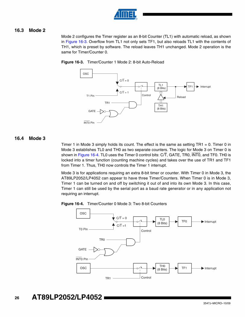
16.3 Mode 2Mode 2 configures the Timer register as an 8-bit Counter (TL1) with automatic reload, as shownin Figure 16-3. Overflow from TL1 not only sets TF1, but also reloads TL1 with the contents ofTH1, which is preset by software. The reload leaves TH1 unchanged. Mode 2 operation is thesame for Timer/Counter 0.
Figure 16-3. Timer/Counter 1 Mode 2: 8-bit Auto-Reload
16.4 Mode 3Timer 1 in Mode 3 simply holds its count. The effect is the same as setting TR1 = 0. Timer 0 inMode 3 establishes TL0 and TH0 as two separate counters. The logic for Mode 3 on Timer 0 isshown in Figure 16-4. TL0 uses the Timer 0 control bits: C/T, GATE, TR0, INT0, and TF0. TH0 islocked into a timer function (counting machine cycles) and takes over the use of TR1 and TF1from Timer 1. Thus, TH0 now controls the Timer 1 interrupt.
Mode 3 is for applications requiring an extra 8-bit timer or counter. With Timer 0 in Mode 3, theAT89LP2052/LP4052 can appear to have three Timer/Counters. When Timer 0 is in Mode 3,Timer 1 can be turned on and off by switching it out of and into its own Mode 3. In this case,Timer 1 can still be used by the serial port as a baud rate generator or in any application notrequiring an interrupt.
Figure 16-4. Timer/Counter 0 Mode 3: Two 8-bit Counters
OSC
T1 Pin
TR1
GATE
TF1TL1(8 Bits)
TH1(8 Bits)
ControlReload
Interrupt
INT0 Pin
C/T = 0
C/T = 1
Control
Interrupt
Control
Interrupt(8 Bits)
(8 Bits)
C/T = 0
C/T =1 T0 Pin
GATE
INT0 Pin
263547J–MICRO–10/09
AT89LP2052/LP4052
AT89LP2052/LP4052
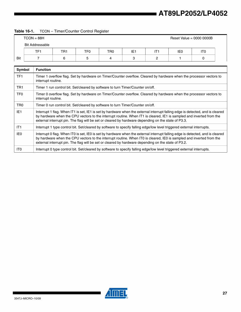
Table 16-1. TCON – Timer/Counter Control Register
TCON = 88H Reset Value = 0000 0000B
Bit Addressable
TF1 TR1 TF0 TR0 IE1 IT1 IE0 IT0
Bit 7 6 5 4 3 2 1 0
Symbol Function
TF1 Timer 1 overflow flag. Set by hardware on Timer/Counter overflow. Cleared by hardware when the processor vectors to interrupt routine.
TR1 Timer 1 run control bit. Set/cleared by software to turn Timer/Counter on/off.
TF0 Timer 0 overflow flag. Set by hardware on Timer/Counter overflow. Cleared by hardware when the processor vectors to interrupt routine.
TR0 Timer 0 run control bit. Set/cleared by software to turn Timer/Counter on/off.
IE1 Interrupt 1 flag. When IT1 is set, IE1 is set by hardware when the external interrupt falling edge is detected, and is cleared by hardware when the CPU vectors to the interrupt routine. When IT1 is cleared, IE1 is sampled and inverted from the external interrupt pin. The flag will be set or cleared by hardware depending on the state of P3.3.
IT1 Interrupt 1 type control bit. Set/cleared by software to specify falling edge/low level triggered external interrupts.
IE0 Interrupt 0 flag. When IT0 is set, IE0 is set by hardware when the external interrupt falling edge is detected, and is cleared by hardware when the CPU vectors to the interrupt routine. When IT0 is cleared, IE0 is sampled and inverted from the external interrupt pin. The flag will be set or cleared by hardware depending on the state of P3.2.
IT0 Interrupt 0 type control bit. Set/cleared by software to specify falling edge/low level triggered external interrupts.
273547J–MICRO–10/09
.
.
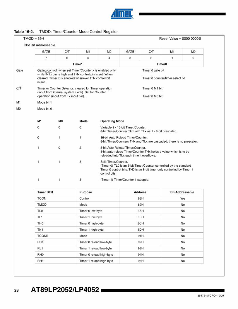
Table 16-2. TMOD: Timer/Counter Mode Control Register
TMOD = 89H Reset Value = 0000 0000B
Not Bit Addressable
GATE C/T M1 M0 GATE C/T M1 M0
7 6 5 4 3 2 1 0
Timer1 Timer0
Gate Gating control: when set Timer/Counter x is enabled only while INTx pin is high and TRx control pin is set. When cleared, Timer x is enabled whenever TRx control bit is set.
Timer 0 gate bit
Timer 0 counter/timer select bit
C/T Timer or Counter Selector: cleared for Timer operation (input from internal system clock). Set for Counter operation (input from Tx input pin).
Timer 0 M1 bit
Timer 0 M0 bit
M1 Mode bit 1
M0 Mode bit 0
M1 M0 Mode Operating Mode
0 0 0 Variable 9 - 16-bit Timer/Counter.8-bit Timer/Counter THz with TLx as 1 - 8-bit prescaler.
0 1 1 16-bit Auto Reload Timer/Counter.8-bit Timer/Counters THx and TLx are cascaded; there is no prescaler.
1 0 2 8-bit Auto Reload Timer/Counter.8-bit auto-reload Timer/Counter THx holds a value which is to be reloaded into TLx each time it overflows.
1 1 3 Split Timer/Counter.(Timer 0) TL0 is an 8-bit Timer/Counter controlled by the standard Timer 0 control bits. TH0 is an 8-bit timer only controlled by Timer 1 control bits.
1 1 3 (Timer 1) Timer/Counter 1 stopped.
Timer SFR Purpose Address Bit-Addressable
TCON Control 88H Yes
TMOD Mode 89H No
TL0 Timer 0 low-byte 8AH No
TL1 Timer 1 low-byte 8BH No
TH0 Timer 0 high-byte 8CH No
TH1 Timer 1 high-byte 8DH No
TCONB Mode 91H No
RL0 Timer 0 reload low-byte 92H No
RL1 Timer 1 reload low-byte 93H No
RH0 Timer 0 reload high-byte 94H No
RH1 Timer 1 reload high-byte 95H No
283547J–MICRO–10/09
AT89LP2052/LP4052
AT89LP2052/LP4052
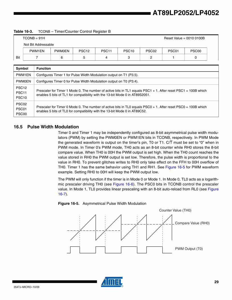
16.5 Pulse Width ModulationTimer 0 and Timer 1 may be independently configured as 8-bit asymmetrical pulse width modu-lators (PWM) by setting the PWM0EN or PWM1EN bits in TCONB, respectively. In PWM Modethe generated waveform is output on the timer's pin, T0 or T1. C/T must be set to “0” when inPWM mode. In Timer 0's PWM mode, TH0 acts as an 8-bit counter while RH0 stores the 8-bitcompare value. When TH0 is 00H the PWM output is set high. When the TH0 count reaches thevalue stored in RH0 the PWM output is set low. Therefore, the pulse width is proportional to thevalue in RH0. To prevent glitches writes to RH0 only take effect on the FFH to 00H overflow ofTH0. Timer 1 has the same behavior using TH1 and RH1. See Figure 16-5 for PWM waveformexample. Setting RH0 to 00H will keep the PWM output low.
The PWM will only function if the timer is in Mode 0 or Mode 1. In Mode 0, TL0 acts as a logarith-mic prescaler driving TH0 (see Figure 16-6). The PSC0 bits in TCONB control the prescalervalue. In Mode 1, TL0 provides linear prescaling with an 8-bit auto-reload from RL0 (see Figure16-7).
Figure 16-5. Asymmetrical Pulse Width Modulation
Table 16-3. TCONB – Timer/Counter Control Register B
TCONB = 91H Reset Value = 0010 0100B
Not Bit Addressable
PWM1EN PWM0EN PSC12 PSC11 PSC10 PSC02 PSC01 PSC00
Bit 7 6 5 4 3 2 1 0
Symbol Function
PWM1EN Configures Timer 1 for Pulse Width Modulation output on T1 (P3.5).
PWM0EN Configures Timer 0 for Pulse Width Modulation output on T0 (P3.4).
PSC12PSC11
PSC10
Prescaler for Timer 1 Mode 0. The number of active bits in TL1 equals PSC1 + 1. After reset PSC1 = 100B which enables 5 bits of TL1 for compatibility with the 13-bit Mode 0 in AT89S2051.
PSC02
PSC01
PSC00
Prescaler for Timer 0 Mode 0. The number of active bits in TL0 equals PSC0 + 1. After reset PSC0 = 100B which enables 5 bits of TL0 for compatibility with the 13-bit Mode 0 in AT89C52.
PWM Output (T0)
Counter Value (TH0)
Compare Value (RH0)
293547J–MICRO–10/09
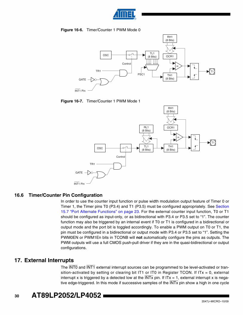
Figure 16-6. Timer/Counter 1 PWM Mode 0
Figure 16-7. Timer/Counter 1 PWM Mode 1
16.6 Timer/Counter Pin ConfigurationIn order to use the counter input function or pulse width modulation output feature of Timer 0 orTimer 1, the Timer pins T0 (P3.4) and T1 (P3.5) must be configured appropriately. See Section15.7 “Port Alternate Functions” on page 23. For the external counter input function, T0 or T1should be configured as input-only, or as bidirectional with P3.4 or P3.5 set to “1”. The counterfunction may also be triggered by an internal event if T0 or T1 is configured in a bidirectional oroutput mode and the port bit is toggled accordingly. To enable a PWM output on T0 or T1, thepin must be configured in a bidirectional or output mode with P3.4 or P3.5 set to “1”. Setting thePWM0EN or PWM1En bits in TCONB will not automatically configure the pins as outputs. ThePWM outputs will use a full CMOS push-pull driver if they are in the quasi-bidirectional or outputconfigurations.
17. External InterruptsThe INT0 and INT1 external interrupt sources can be programmed to be level-activated or tran-sition-activated by setting or clearing bit IT1 or IT0 in Register TCON. If ITx = 0, externalinterrupt x is triggered by a detected low at the INTx pin. If ITx = 1, external interrupt x is nega-tive edge-triggered. In this mode if successive samples of the INTx pin show a high in one cycle
OSC
TR1
GATE
INT1 Pin
TL1(8 Bits)
Control
PSC1 TH1(8 Bits)
OCR1
RH1(8 Bits)
=T1
OSC
TR1
GATE
INT1 Pin
TL1(8 Bits)
Control
TH1(8 Bits)
OCR1
RH1(8 Bits)
=T1
RL1(8 Bits)
303547J–MICRO–10/09
AT89LP2052/LP4052
AT89LP2052/LP4052
and a low in the next cycle, interrupt request flag IEx in TCON is set. Flag bit IEx then requeststhe interrupt. Since the external interrupt pins are sampled once each clock cycle, an input highor low should hold for at least 2 oscillator periods to ensure sampling. If the external interrupt istransition-activated, the external source has to hold the request pin high for at least two clockcycles, and then hold it low for at least two clock cycles to ensure that the transition is seen sothat interrupt request flag IEx will be set. IEx will be automatically cleared by the CPU when theservice routine is called if generated in edge-triggered mode. If the external interrupt is level-acti-vated, the external source has to hold the request active until the requested interrupt is actuallygenerated. Then the external source must deactivate the request before the interrupt serviceroutine is completed, or else another interrupt will be generated.
18. Serial InterfaceThe serial port is full-duplex, which means it can transmit and receive simultaneously. It is alsoreceive-buffered, which means it can begin receiving a second byte before a previously receivedbyte has been read from the receive register. (However, if the first byte still has not been readwhen reception of the second byte is complete, the first byte will be lost.) The serial port receiveand transmit registers are both accessed at Special Function Register SBUF. Writing to SBUFloads the transmit register, and reading SBUF accesses a physically separate receive register.The serial port can operate in the following four modes.
Mode 0: Half-Duplex serial data enters or exits through RXD. TXD outputs the shift clock. Eightdata bits are transmitted/received, with the LSB first. The baud rate is fixed at 1/2 the oscillatorfrequency.
Mode 1: 10 bits are transmitted (through TXD) or received (through RXD): a start bit (0), 8 databits (LSB first), and a stop bit (1). On receive, the stop bit goes into RB8 in Special FunctionRegister SCON. The baud rate is variable based on Timer 1 overflow.
Mode 2: 11 bits are transmitted (through TXD) or received (through RXD): a start bit (0), 8 databits (LSB first), a programmable ninth data bit, and a stop bit (1). On transmit, the 9th data bit(TB8 in SCON) can be assigned the value of “0” or “1”. For example, the parity bit (P, in thePSW) can be moved into TB8. On receive, the 9th data bit goes into RB8 in Special FunctionRegister SCON, while the stop bit is ignored. The baud rate is programmable to either 1/16 or1/32 the oscillator frequency.
Mode 3: 11 bits are transmitted (through TXD) or received (through RXD): a start bit (0), 8 databits (LSB first), a programmable ninth data bit, and a stop bit (1). In fact, Mode 3 is the same asMode 2 in all respects except the baud rate, which in Mode 3 is variable based on Timer 1overflow.
In all four modes, transmission is initiated by any instruction that uses SBUF as a destinationregister. Reception is initiated in Mode 0 by the condition RI = 0 and REN = 1. Reception is initi-ated in the other modes by the incoming start bit if REN = 1.
18.1 Multiprocessor CommunicationsModes 2 and 3 have a special provision for multiprocessor communications. In these modes, 9data bits are received, followed by a stop bit. The ninth bit goes into RB8. Then comes a stop bit.The port can be programmed such that when the stop bit is received, the serial port interrupt isactivated only if RB8 = 1. This feature is enabled by setting bit SM2 in SCON.
The following example shows how to use the serial interrupt for multiprocessor communications.When the master processor must transmit a block of data to one of several slaves, it first sends
313547J–MICRO–10/09
out an address byte that identifies the target slave. An address byte differs from a data byte inthat the 9th bit is “1” in an address byte and “0” in a data byte. With SM2 = 1, no slave is inter-rupted by a data byte. An address byte, however, interrupts all slaves, so that each slave canexamine the received byte and see if it is being addressed. The addressed slave clears its SM2bit and prepares to receive the data bytes that follows. The slaves that are not addressed settheir SM2 bits and ignore the data bytes.
The SM2 bit has no effect in Mode 0 but can be used to check the validity of the stop bit inMode 1. In a Mode 1 reception, if SM2 = 1, the receive interrupt is not activated unless a validstop bit is received.
Notes: 1. SMOD0 is located at PCON.6.2. fosc = oscillator frequency.
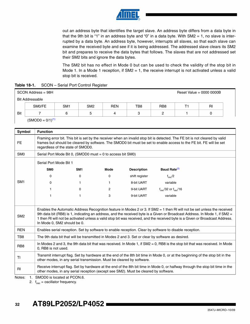
Table 18-1. SCON – Serial Port Control Register
SCON Address = 98H Reset Value = 0000 0000B
Bit Addressable
SM0/FE SM1 SM2 REN TB8 RB8 T1 RI
Bit 7 6 5 4 3 2 1 0
(SMOD0 = 0/1)(1)
Symbol Function
FEFraming error bit. This bit is set by the receiver when an invalid stop bit is detected. The FE bit is not cleared by valid frames but should be cleared by software. The SMOD0 bit must be set to enable access to the FE bit. FE will be set regardless of the state of SMOD0.
SM0 Serial Port Mode Bit 0, (SMOD0 must = 0 to access bit SM0)
SM1
Serial Port Mode Bit 1
SM2
Enables the Automatic Address Recognition feature in Modes 2 or 3. If SM2 = 1 then Rl will not be set unless the received 9th data bit (RB8) is 1, indicating an address, and the received byte is a Given or Broadcast Address. In Mode 1, if SM2 = 1 then Rl will not be activated unless a valid stop bit was received, and the received byte is a Given or Broadcast Address. In Mode 0, SM2 should be 0.
REN Enables serial reception. Set by software to enable reception. Clear by software to disable reception.
TB8 The 9th data bit that will be transmitted in Modes 2 and 3. Set or clear by software as desired.
RB8In Modes 2 and 3, the 9th data bit that was received. In Mode 1, if SM2 = 0, RB8 is the stop bit that was received. In Mode 0, RB8 is not used.
TITransmit interrupt flag. Set by hardware at the end of the 8th bit time in Mode 0, or at the beginning of the stop bit in the other modes, in any serial transmission. Must be cleared by software.
RIReceive interrupt flag. Set by hardware at the end of the 8th bit time in Mode 0, or halfway through the stop bit time in the other modes, in any serial reception (except see SM2). Must be cleared by software.
SM0 SM1 Mode Description Baud Rate(2)
0 0 0 shift register fosc/2
0 1 1 8-bit UART variable
1 0 2 9-bit UART fosc/32 or fosc/16
1 1 3 9-bit UART variable
323547J–MICRO–10/09
AT89LP2052/LP4052
AT89LP2052/LP4052
18.2 Baud RatesThe baud rate in Mode 0 is fixed as shown in the following equation.
The baud rate in Mode 2 depends on the value of the SMOD1 bit in Special Function RegisterPCON.7. If SMOD1 = 0 (the value on reset), the baud rate is 1/32 of the oscillator frequency. IfSMOD1 = 1, the baud rate is 1/16 of the oscillator frequency, as shown in the following equation.
18.2.1 Using Timer 1 to Generate Baud RatesThe Timer 1 overflow rate determines the baud rates in Modes 1 and 3. When Timer 1 is thebaud rate generator, the baud rates are determined by the Timer 1 overflow rate and the valueof SMOD1 according to the following equation.
The Timer 1 interrupt should be disabled in this application. The Timer itself can be configuredfor either timer or counter operation in any of its 3 running modes. In the most typical applica-tions, it is configured for timer operation in auto-reload mode (high nibble of TMOD = 0010B). Inthis case, the baud rate is given by the following formula.
Programmers can achieve very low baud rates with Timer 1 by configuring the Timer to run as a16-bit auto-reload timer (high nibble of TMOD = 0001B). In this case, the baud rate is given bythe following formula.
Mode 0 Baud Rate Oscillator Frequency2
-------------------------------------------------------=
Mode 2 Baud Rate2
SMOD1
32-------------------- (Oscillator Frequency)×=
2SMOD1
32-------------------- (Timer 1 Overflow Rate)×=Modes 1, 3
Baud Rate
2SMOD1
32-------------------- Oscillator Frequency
256 TH1( )–[ ]-------------------------------------------------------×=Modes 1, 3
Baud Rate
2SMOD1
32-------------------- Oscillator Frequency
65536 RH1,RL1( )–[ ]---------------------------------------------------------×=Modes 1, 3
Baud Rate
333547J–MICRO–10/09
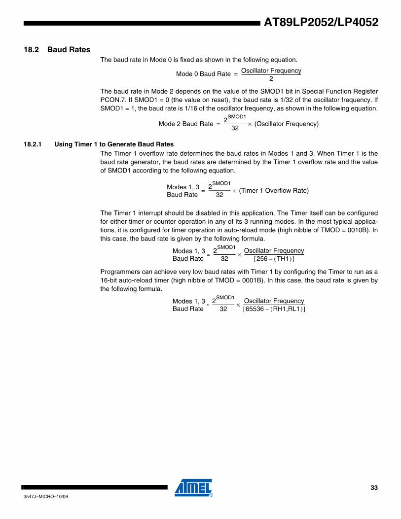
Table 18-2 lists commonly used baud rates and how they can be obtained from Timer 1.
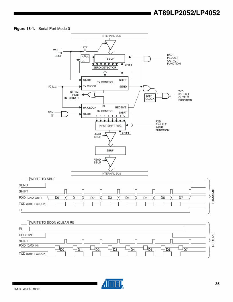
18.3 More About Mode 0Serial data enters and exits through RXD. TXD outputs the shift clock. Eight data bits are trans-mitted/received, with the LSB first. The baud rate is fixed at 1/2 the oscillator frequency. Figure18-1 shows a simplified functional diagram of the serial port in Mode 0 and associated timing.
Transmission is initiated by any instruction that uses SBUF as a destination register. The “writeto SBUF” signal also loads a “1” into the ninth position of the transmit shift register and tells theTX Control block to begin a transmission. The internal timing is such that one full machine cyclewill elapse between “write to SBUF” and activation of SEND.
SEND transfers the output of the shift register to the alternate output function line of P3.0, andalso transfers Shift Clock to the alternate output function line of P3.1. At the falling edge of ShiftClock the contents of the transmit shift register are shifted one position to the right.
As data bits shift out to the right, “0”s come in from the left. When the MSB of the data byte is atthe output position of the shift register, the “1” that was initially loaded into the ninth position isjust to the left of the MSB, and all positions to the left of that contain “0”s. This condition flags theTX Control block to do one last shift, then deactivate SEND and set TI.
Reception is initiated by the condition REN = 1 and R1 = 0. At the next clock cycle, the RX Con-trol unit writes the bits 11111110 to the receive shift register and activates RECEIVE in the nextclock phase.
RECEIVE enables Shift Clock to the alternate output function line of P3.1. At the falling edge ofShift Clock the contents of the receive shift register are shifted one position to the left. The valuethat comes in from the right is the value that was sampled at the P3.0 pin at rising edge of ShiftClock.
As data bits come in from the right, “1”s shift out to the left. When the “0” that was initially loadedinto the right-most position arrives at the left-most position in the shift register, it flags the RXControl block to do one last shift and load SBUF. Then RECEIVE is cleared and RI is set.
Table 18-2. Commonly Used Baud Rates Generated by Timer 1
Baud Rate fOSC (MHz) SMOD1
Timer 1
C/T Mode Reload Value
Mode 0: 1 MHz 2 X X X X
Mode 2: 375K 12 0 X X X
62.5K 12 1 0 2 F4H
19.2K 11.059 1 0 2 DCH
9.6K 11.059 0 0 2 DCH
4.8K 11.059 0 0 2 B8H
2.4K 11.059 0 0 2 70H
1.2K 11.059 0 0 1 FEE0H
137.5 11.986 0 0 1 F55CH
110 6 0 0 1 F958H
110 12 0 0 1 F304H
343547J–MICRO–10/09
AT89LP2052/LP4052
AT89LP2052/LP4052
Figure 18-1. Serial Port Mode 0
INTERNAL BUS
1/2 fosc
INTERNAL BUS
TXD (SHIFT CLOCK)
RXD (DATA OUT)
TXD (SHIFT CLOCK)
RXD (DATA IN)
WRITE TO SBUF
SEND
SHIFT
TI
WRITE TO SCON (CLEAR RI)
SHIFT
RECEIVE
RI
“1“
353547J–MICRO–10/09
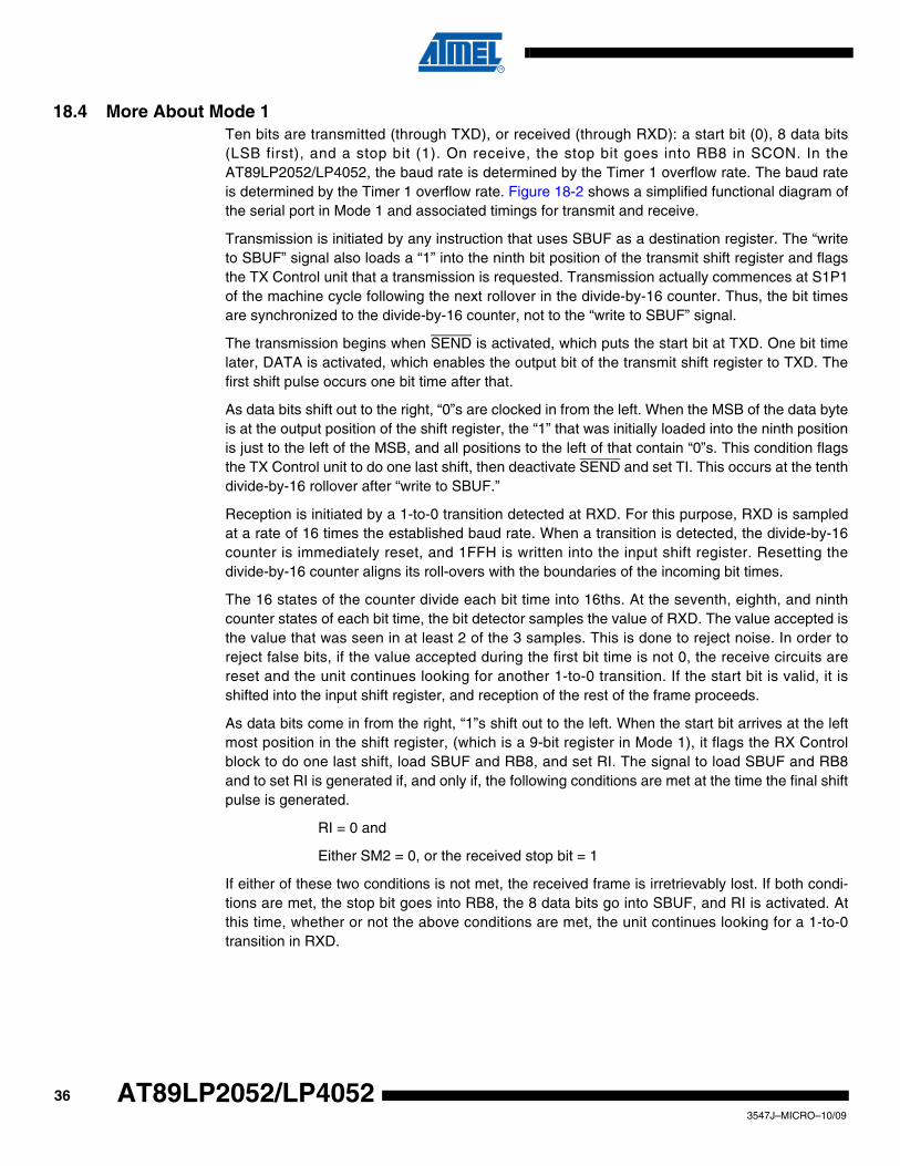
18.4 More About Mode 1Ten bits are transmitted (through TXD), or received (through RXD): a start bit (0), 8 data bits(LSB first), and a stop bit (1). On receive, the stop bit goes into RB8 in SCON. In theAT89LP2052/LP4052, the baud rate is determined by the Timer 1 overflow rate. The baud rateis determined by the Timer 1 overflow rate. Figure 18-2 shows a simplified functional diagram ofthe serial port in Mode 1 and associated timings for transmit and receive.
Transmission is initiated by any instruction that uses SBUF as a destination register. The “writeto SBUF” signal also loads a “1” into the ninth bit position of the transmit shift register and flagsthe TX Control unit that a transmission is requested. Transmission actually commences at S1P1of the machine cycle following the next rollover in the divide-by-16 counter. Thus, the bit timesare synchronized to the divide-by-16 counter, not to the “write to SBUF” signal.
The transmission begins when SEND is activated, which puts the start bit at TXD. One bit timelater, DATA is activated, which enables the output bit of the transmit shift register to TXD. Thefirst shift pulse occurs one bit time after that.
As data bits shift out to the right, “0”s are clocked in from the left. When the MSB of the data byteis at the output position of the shift register, the “1” that was initially loaded into the ninth positionis just to the left of the MSB, and all positions to the left of that contain “0”s. This condition flagsthe TX Control unit to do one last shift, then deactivate SEND and set TI. This occurs at the tenthdivide-by-16 rollover after “write to SBUF.”
Reception is initiated by a 1-to-0 transition detected at RXD. For this purpose, RXD is sampledat a rate of 16 times the established baud rate. When a transition is detected, the divide-by-16counter is immediately reset, and 1FFH is written into the input shift register. Resetting thedivide-by-16 counter aligns its roll-overs with the boundaries of the incoming bit times.
The 16 states of the counter divide each bit time into 16ths. At the seventh, eighth, and ninthcounter states of each bit time, the bit detector samples the value of RXD. The value accepted isthe value that was seen in at least 2 of the 3 samples. This is done to reject noise. In order toreject false bits, if the value accepted during the first bit time is not 0, the receive circuits arereset and the unit continues looking for another 1-to-0 transition. If the start bit is valid, it isshifted into the input shift register, and reception of the rest of the frame proceeds.
As data bits come in from the right, “1”s shift out to the left. When the start bit arrives at the leftmost position in the shift register, (which is a 9-bit register in Mode 1), it flags the RX Controlblock to do one last shift, load SBUF and RB8, and set RI. The signal to load SBUF and RB8and to set RI is generated if, and only if, the following conditions are met at the time the final shiftpulse is generated.
RI = 0 and
Either SM2 = 0, or the received stop bit = 1
If either of these two conditions is not met, the received frame is irretrievably lost. If both condi-tions are met, the stop bit goes into RB8, the 8 data bits go into SBUF, and RI is activated. Atthis time, whether or not the above conditions are met, the unit continues looking for a 1-to-0transition in RXD.
363547J–MICRO–10/09
AT89LP2052/LP4052
AT89LP2052/LP4052
Figure 18-2. Serial Port Mode 1
TXCLOCK
WRITE TO SBUF
INTERNAL BUS
READSBUF
LOADSBUF
SBUF
SHIFT
INPUT SHIFT REG.(9 BITS)
BITDETECTOR
1-TO-0TRANSITIONDETECTOR
SERIALPORT
INTERRUPT
WRITETO
SBUF÷2
SMOD1= 0
SMOD1= 1
TIMER 1OVERFLOW
RXD
RX CLOCK
RX CLOCK
RX CONTROLSTART
START DATA
SEND
SAMPLE
÷16
÷16TX CONTROL
TITI
ZERO DETECTOR
SBUFTXD
INTERNAL BUS
“1”
D QCL
S
LOADSBUFSHIFT
SHIFT
1FFH
RI
SEND
DATA
SHIFT
TXD
TI
D0 D1 D2 D3 D4 D5 D6 D7
D0 D1 D2 D3 D4 D5 D6 D7
STOP BIT
TR
AN
SM
IT
START BIT
÷16 RESET
START BIT STOP BIT
RXCLOCK
BIT DETECTOR SAMPLE TIMES
SHIFT
RE
CE
IVE RXD
RI
373547J–MICRO–10/09
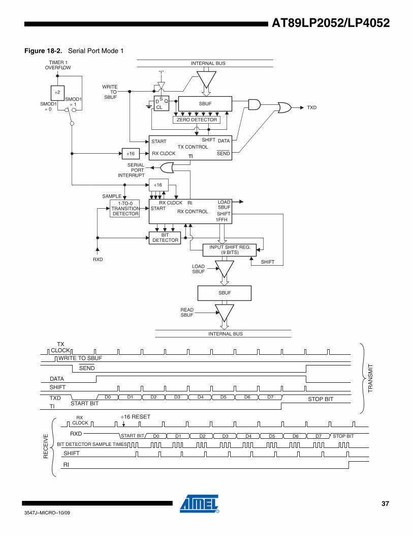
18.5 More About Modes 2 and 3Eleven bits are transmitted (through TXD), or received (through RXD): a start bit (0), 8 data bits(LSB first), a programmable ninth data bit, and a stop bit (1). On transmit, the ninth data bit (TB8)can be assigned the value of “0” or “1”. On receive, the ninth data bit goes into RB8 in SCON.The baud rate is programmable to either 1/16 or 1/32 of the oscillator frequency in Mode 2.Mode 3 may have a variable baud rate generated from Timer 1.
Figures 18-3 and 18-4 show a functional diagram of the serial port in Modes 2 and 3. Thereceive portion is exactly the same as in Mode 1. The transmit portion differs from Mode 1 onlyin the ninth bit of the transmit shift register.
Transmission is initiated by any instruction that uses SBUF as a destination register. The “writeto SBUF” signal also loads TB8 into the ninth bit position of the transmit shift register and flagsthe TX Control unit that a transmission is requested. Transmission commences at S1P1 of themachine cycle following the next rollover in the divide-by-16 counter. Thus, the bit times are syn-chronized to the divide-by-16 counter, not to the “write to SBUF” signal.
The transmission begins when SEND is activated, which puts the start bit at TXD. One bit timelater, DATA is activated, which enables the output bit of the transmit shift register to TXD. Thefirst shift pulse occurs one bit time after that. The first shift clocks a “1” (the stop bit) into the ninthbit position of the shift register. Thereafter, only “0”s are clocked in. Thus, as data bits shift out tothe right, “0”s are clocked in from the left. When TB8 is at the output position of the shift register,then the stop bit is just to the left of TB8, and all positions to the left of that contain “0”s. This con-dition flags the TX Control unit to do one last shift, then deactivate SEND and set TI. This occursat the 11th divide-by-16 rollover after “write to SBUF.”
Reception is initiated by a 1-to-0 transition detected at RXD. For this purpose, RXD is sampledat a rate of 16 times the established baud rate. When a transition is detected, the divide-by-16counter is immediately reset, and 1FFH is written to the input shift register.
At the seventh, eighth and ninth counter states of each bit time, the bit detector samples thevalue of RXD. The value accepted is the value that was seen in at least 2 of the 3 samples. If thevalue accepted during the first bit time is not 0, the receive circuits are reset and the unit contin-ues looking for another 1-to-0 transition. If the start bit proves valid, it is shifted into the input shiftregister, and reception of the rest of the frame proceeds.
As data bits come in from the right, “1”s shift out to the left. When the start bit arrives at the leftmost position in the shift register (which in Modes 2 and 3 is a 9-bit register), it flags the RX Con-trol block to do one last shift, load SBUF and RB8, and set RI. The signal to load SBUF and RB8and to set RI is generated if, and only if, the following conditions are met at the time the final shiftpulse is generated:
RI = 0, and
Either SM2 = 0 or the received 9th data bit = 1
If either of these conditions is not met, the received frame is irretrievably lost, and RI is not set. Ifboth conditions are met, the received ninth data bit goes into RB8, and the first 8 data bits gointo SBUF. One bit time later, whether the above conditions were met or not, the unit continueslooking for a 1-to-0 transition at the RXD input.
Note that the value of the received stop bit is irrelevant to SBUF, RB8, or RI.
383547J–MICRO–10/09
AT89LP2052/LP4052
AT89LP2052/LP4052
Figure 18-3. Serial Port Mode 2
SMOD1 1
SMOD1 0
INTERNAL BUS
INTERNAL BUS
CPU CLOCK
393547J–MICRO–10/09
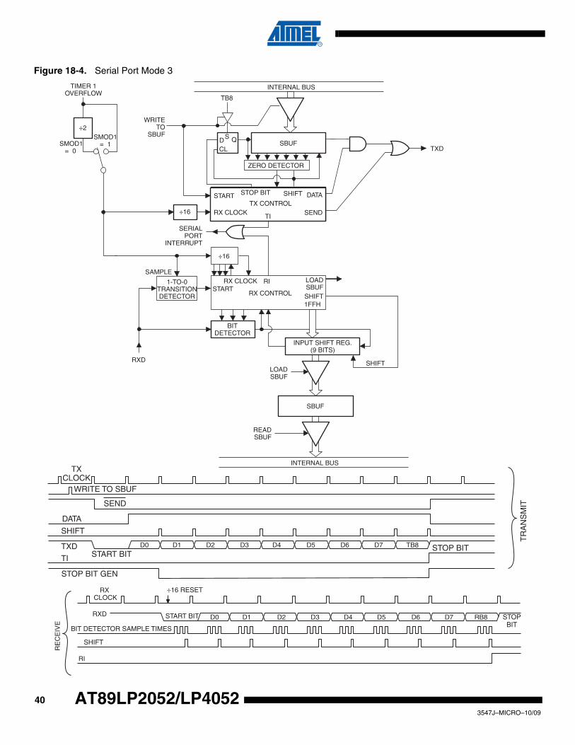
Figure 18-4. Serial Port Mode 3
TXCLOCK
WRITE TO SBUF
SEND
DATA
SHIFT
TXD
STOP BIT GEN
TI
D0 D1 D2 D3 D4 D5 D6 D7 TB8 STOP BIT
TR
AN
SM
IT
START BIT
INTERNAL BUS
READSBUF
LOADSBUF
SBUF
SHIFT
INPUT SHIFT REG.(9 BITS)
BITDETECTOR
1-TO-0TRANSITIONDETECTOR
SERIALPORT
INTERRUPT
WRITETO
SBUF÷2
SMOD1= 0
SMOD1= 1
TIMER 1OVERFLOW
RXD
RX CLOCK
RX CLOCK
RX CONTROLSTART
START DATA
SAMPLE
÷16
÷16
TX CONTROL
TI
ZERO DETECTOR
SBUFTXD
INTERNAL BUS
TB8
D QCL
S
LOADSBUFSHIFT1FFH
SHIFT
RI
SEND
D0 D1 D2 D3 D4 D5 D6 D7 RB8START BIT STOPBIT
÷16 RESETRXCLOCK
BIT DETECTOR SAMPLE TIMES
SHIFT
RE
CE
IVE
RXD
RI
STOP BIT
403547J–MICRO–10/09
AT89LP2052/LP4052
AT89LP2052/LP4052
18.6 Framing Error DetectionWhen used for framing error detect, the UART looks for missing stop bits in the communication.A missing bit will set the FE bit in the SCON register. The FE bit shares the SCON.7 bit with SM0and the function of SCON.7 is determined by PCON.6 (SMOD0). If SMOD0 is set then SCON.7functions as FE. SCON.7 functions as SM0 when SMOD0 is cleared. When used as FE,SCON.7 can only be cleared by software.
18.7 Automatic Address RecognitionAutomatic Address Recognition is a feature which allows the UART to recognize certainaddresses in the serial bit stream by using hardware to make the comparisons. This featuresaves a great deal of software overhead by eliminating the need for the software to examineevery serial address which passes by the serial port. This feature is enabled by setting the SM2bit in SCON. In the 9-bit UART modes, Mode 2 and Mode 3, the Receive Interrupt flag (RI) willbe automatically set when the received byte contains either the “Given” address or the “Broad-cast” address. The 9-bit mode requires that the 9th information bit is a “1” to indicate that thereceived information is an address and not data.
The 8-bit mode is called Mode 1. In this mode the RI flag will be set if SM2 is enabled and theinformation received has a valid stop bit following the 8 address bits and the information is eithera Given or Broadcast address.
Mode 0 is the Shift Register mode and SM2 is ignored.
Using the Automatic Address Recognition feature allows a master to selectively communicatewith one or more slaves by invoking the given slave address or addresses. All of the slaves maybe contacted by using the Broadcast address. Two special Function Registers are used todefine the slave’s address, SADDR, and the address mask, SADEN. SADEN is used to definewhich bits in the SADDR are to be used and which bits are “don’t care”. The SADEN mask canbe logically ANDed with the SADDR to create the “Given” address which the master will use foraddressing each of the slaves. Use of the Given address allows multiple slaves to be recognizedwhile excluding others. The following examples will help to show the versatility of this scheme:
Slave 0 SADDR = 1100 0000
SADEN = 1111 1101
Given = 1100 00X0
Slave 1 SADDR = 1100 0000
SADEN = 1111 1110
Given = 1100 000X
In the previous example SADDR is the same and the SADEN data is used to differentiatebetween the two slaves. Slave 0 requires a “0” in bit 0 and it ignores bit 1. Slave 1 requires a “0”in bit 1 and bit 0 is ignored. A unique address for slave 0 would be 1100 0010 since slave 1requires a “0” in bit 1. A unique address for slave 1 would be 1100 0001 since a “1” in bit 0 willexclude slave 0. Both slaves can be selected at the same time by an address which has bit 0 = 0(for slave 0) and bit 1 = 0 (for slave 1). Thus, both could be addressed with 1100 0000.
413547J–MICRO–10/09
In a more complex system the following could be used to select slaves 1 and 2 while excludingslave 0:
Slave 0 SADDR = 1100 0000
SADEN = 1111 1001
Given = 1100 0XX0
Slave 1 SADDR = 1110 0000
SADEN = 1111 1010
Given = 1110 0X0X
Slave 2 SADDR = 1110 0000
SADEN = 1111 1100
Given = 1110 00XX
In the above example the differentiation among the 3 slaves is in the lower 3 address bits. Slave0 requires that bit 0 = 0 and it can be uniquely addressed by 1110 0110. Slave 1 requires that bit1 = 0 and it can be uniquely addressed by 1110 and 0101. Slave 2 requires that bit 2 = 0 and itsunique address is 1110 0011. To select Slaves 0 and 1 and exclude Slave 2, use address 11100100, since it is necessary to make bit 2 = 1 to exclude slave 2.
The Broadcast Address for each slave is created by taking the logic OR of SADDR and SADEN.Zeros in this result are treated as don’t cares. In most cases, interpreting the don’t cares asones, the broadcast address will be FF hexadecimal.
Upon reset SADDR (SFR address 0A9H) and SADEN (SFR address 0B9H) are loaded with“0”s. This produces a given address of all “don’t cares” as well as a Broadcast address of all“don’t cares”. This effectively disables the Automatic Addressing mode and allows the microcon-troller to use standard 80C51-type UART drivers which do not make use of this feature.
19. Serial Peripheral InterfaceThe serial peripheral interface (SPI) allows high-speed synchronous data transfer between theAT89LP2052/LP4052 and peripheral devices or between multiple AT89LP2052/LP4052devices. The AT89LP2052/LP4052 SPI features include the following:
• Full-duplex, 3-wire Synchronous Data Transfer
• Master or Slave Operation
• Maximum Bit Frequency = f/4
• LSB First or MSB First Data Transfer
• Four Programmable Bit Rates in Master Mode
• End of Transmission Interrupt Flag
• Write Collision Flag Protection
• Double-buffered Receive
• Double-buffered Transmit (Enhanced Mode Only)
• Wake up from Idle Mode (Slave Mode Only)
423547J–MICRO–10/09
AT89LP2052/LP4052
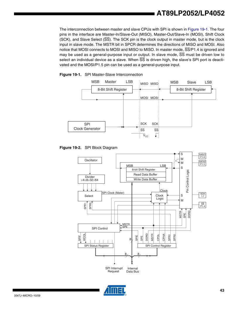
AT89LP2052/LP4052
The interconnection between master and slave CPUs with SPI is shown in Figure 19-1. The fourpins in the interface are Master-In/Slave-Out (MISO), Master-Out/Slave-In (MOSI), Shift Clock(SCK), and Slave Select (SS). The SCK pin is the clock output in master mode, but is the clockinput in slave mode. The MSTR bit in SPCR determines the directions of MISO and MOSI. Alsonotice that MOSI connects to MOSI and MISO to MISO. In master mode, SS/P1.4 is ignored andmay be used as a general-purpose input or output. In slave mode, SS must be driven low toselect an individual device as a slave. When SS is driven high, the slave’s SPI port is deacti-vated and the MOSI/P1.5 pin can be used as a general-purpose input.
Figure 19-1. SPI Master-Slave Interconnection
Figure 19-2. SPI Block Diagram
8-Bit Shift Register 8-Bit Shift Register
Master
Clock GeneratorSPI
MISO SlaveMISO
MOSI MOSI
SCK SCK
SS SS
VCC
MSB LSB MSB LSB
Oscillator
8-bit Shift Register
Read Data Buffer
Pin
Con
trol
Log
ic
SPI Control
SPI Status Register
SPI InterruptRequest
InternalData Bus
SelectSPI Clock (Mater)
Divider÷4÷8÷32÷64
SPI Control Register
8
8
8
SP
IF
WC
OL
SP
R1
MSTR
SP
IE
ClockLogic
Clock
MSB
S
M
SP
E
DO
RD
MS
TR
CP
OL
CP
HA
SP
R1
SP
R0
MS
TR
SP
E
DO
RD
LSB
S
MM
S
MISOP1.6
MOSIP1.5
SCK1.7
SSP1.4
SP
R0
SPE
Write Data Buffer
433547J–MICRO–10/09
19.1 Normal ModeThe SPI has two modes of operation: normal (non-buffered write) and enhanced (bufferedwrite). In normal mode, writing to the SPI data register (SPDR) of the master CPU starts the SPIclock generator and the data written shifts out of the MOSI pin and into the MOSI pin of the slaveCPU. Transmission may start after an initial delay while the clock generator waits for the next fullbit slot of the specified baud rate. After shifting one byte, the SPI clock generator stops, settingthe end of transmission flag (SPIF) and transferring the received byte to the read buffer (SPDR).If both the SPI interrupt enable bit (SPIE) and the serial port interrupt enable bit (ES) are set, aninterrupt is requested. Note that SPDR refers to either the write data buffer or the read data buf-fer, depending on whether the access is a write or read. In normal mode, because the writebuffer is transparent (and a write access to SPDR will be directed to the shift buffer), any attemptto write to SPDR while a transmission is in progress will result in a write collision with WCOL set.However, the transmission will still complete normally, but the new byte will be ignored and anew write access to SPDR will be necessary.
19.2 Enhanced ModeEnhanced mode is similar to normal mode except that the write buffer holds the next byte to betransmitted. Writing to SPDR loads the write buffer and sets WCOL to signify that the buffer isfull and any further writes will overwrite the buffer. WCOL is cleared by hardware when the buff-ered byte is loaded into the shift register and transmission begins. If the master SPI is currentlyidle, i.e. if this is the first byte, then after loading SPDR, transmission of the byte starts andWCOL is cleared immediately. While this byte is transmitting, the next byte may be written toSPDR. The Load Enable flag (LDEN) in SPSR can be used to determine when transmission hasstarted. LDEN is asserted during the first four bit slots of a SPI transfer. The master CPU shouldfirst check that LDEN is set and that WCOL is cleared before loading the next byte. In enhancedmode, if WCOL is set when a transfer completes, i.e. the next byte is available, then the SPIimmediately loads the buffered byte into the shift register, resets WCOL, and continues trans-mission without stopping and restarting the clock generator. As long as the CPU can keep thewrite buffer full in this manner, multiple bytes may be transferred with minimal latency betweenbytes.
443547J–MICRO–10/09
AT89LP2052/LP4052
AT89LP2052/LP4052
Notes: 1. Set up the clock mode before enabling the SPI: set all bits needed in SPCR except the SPE bit, then set SPE.2. Enable the master SPI prior to the slave device.3. Slave echoes master on the next Tx if not loaded with new data.
Table 19-1. SPCR – SPI Control Register
SPCR Address = D5H Reset Value = 0000 0000B
Not Bit Addressable
SPIE SPE DORD MSTR CPOL CPHA SPR1 SPR0
Bit 7 6 5 4 3 2 1 0
Symbol Function
SPIE SPI interrupt enable. This bit, in conjunction with the ES bit in the IE register, enables SPI interrupts: SPIE = 1 and ES = 1 enable SPI interrupts. SPIE = 0 disables SPI interrupts.
SPE SPI enable. SPE = 1 enables the SPI channel and connects SS, MOSI, MISO and SCK to pins P1.4, P1.5, P1.6, and P1.7. SPE = 0 disables the SPI channel.
DORD Data order. DORD = 1 selects LSB first data transmission. DORD = 0 selects MSB first data transmission.
MSTR Master/slave select. MSTR = 1 selects Master SPI mode. MSTR = 0 selects slave SPI mode.
CPOL Clock polarity. When CPOL = 1, SCK is high when idle. When CPOL = 0, SCK of the master device is low when not transmitting. Please refer to figure on SPI clock phase and polarity control.
CPHA Clock phase. The CPHA bit together with the CPOL bit controls the clock and data relationship between master and slave. Please refer to figure on SPI clock phase and polarity control.
SPR0SPR1
SPI clock rate select. These two bits control the SCK rate of the device configured as master. SPR1 and SPR0 have no effect on the slave. The relationship between SCK and the oscillator frequency, FOSC., is as follows:
SPR1 SPR0 SCK0 0 f/40 1 f/8
1 0 f/32
1 1 f/64
453547J–MICRO–10/09
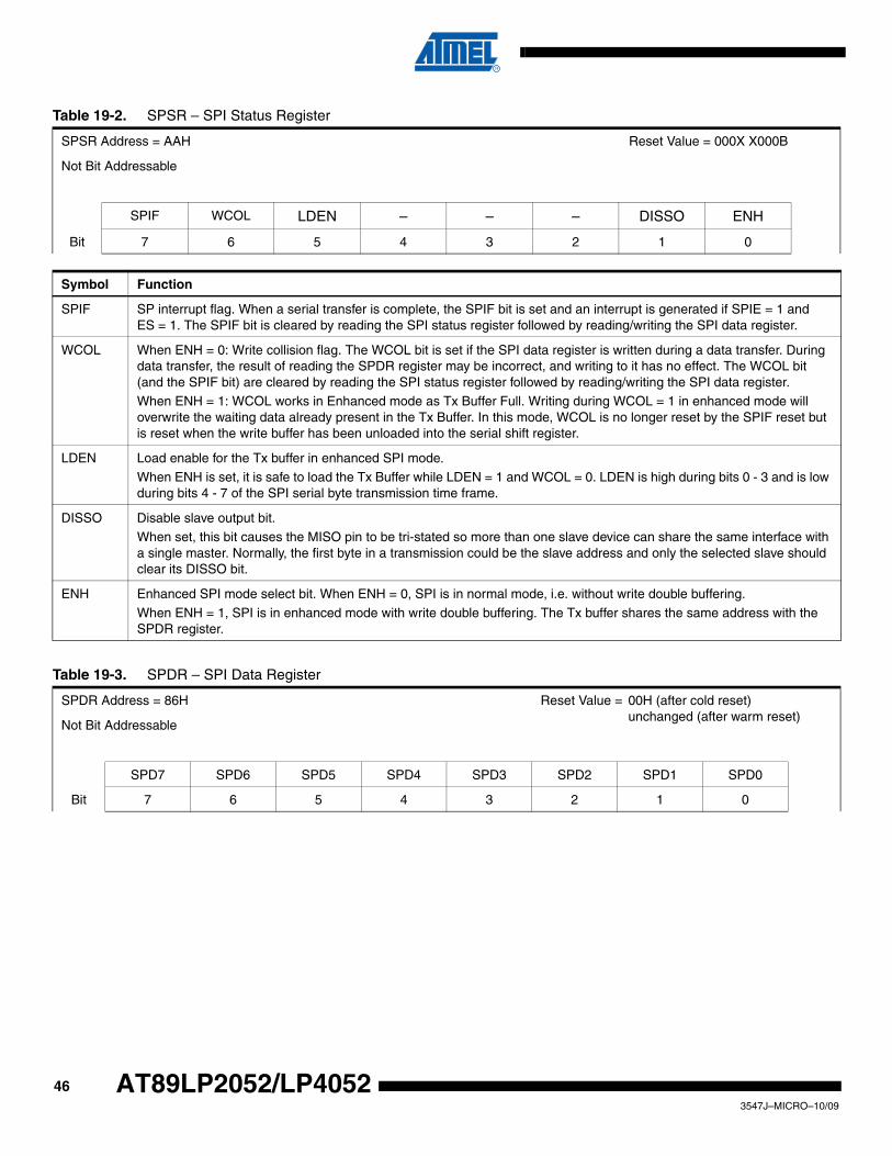
Table 19-2. SPSR – SPI Status Register
SPSR Address = AAH Reset Value = 000X X000B
Not Bit Addressable
SPIF WCOL LDEN – – – DISSO ENH
Bit 7 6 5 4 3 2 1 0
Symbol Function
SPIF SP interrupt flag. When a serial transfer is complete, the SPIF bit is set and an interrupt is generated if SPIE = 1 and ES = 1. The SPIF bit is cleared by reading the SPI status register followed by reading/writing the SPI data register.
WCOL When ENH = 0: Write collision flag. The WCOL bit is set if the SPI data register is written during a data transfer. During data transfer, the result of reading the SPDR register may be incorrect, and writing to it has no effect. The WCOL bit (and the SPIF bit) are cleared by reading the SPI status register followed by reading/writing the SPI data register.When ENH = 1: WCOL works in Enhanced mode as Tx Buffer Full. Writing during WCOL = 1 in enhanced mode will overwrite the waiting data already present in the Tx Buffer. In this mode, WCOL is no longer reset by the SPIF reset but is reset when the write buffer has been unloaded into the serial shift register.
LDEN Load enable for the Tx buffer in enhanced SPI mode.
When ENH is set, it is safe to load the Tx Buffer while LDEN = 1 and WCOL = 0. LDEN is high during bits 0 - 3 and is low during bits 4 - 7 of the SPI serial byte transmission time frame.
DISSO Disable slave output bit.When set, this bit causes the MISO pin to be tri-stated so more than one slave device can share the same interface with a single master. Normally, the first byte in a transmission could be the slave address and only the selected slave should clear its DISSO bit.
ENH Enhanced SPI mode select bit. When ENH = 0, SPI is in normal mode, i.e. without write double buffering.
When ENH = 1, SPI is in enhanced mode with write double buffering. The Tx buffer shares the same address with the SPDR register.
Table 19-3. SPDR – SPI Data Register
SPDR Address = 86H Reset Value = 00H (after cold reset) unchanged (after warm reset)
Not Bit Addressable
SPD7 SPD6 SPD5 SPD4 SPD3 SPD2 SPD1 SPD0
Bit 7 6 5 4 3 2 1 0
463547J–MICRO–10/09
AT89LP2052/LP4052
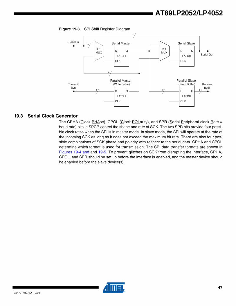
AT89LP2052/LP4052
Figure 19-3. SPI Shift Register Diagram
19.3 Serial Clock GeneratorThe CPHA (Clock PHAse), CPOL (Clock POLarity), and SPR (Serial Peripheral clock Rate =baud rate) bits in SPCR control the shape and rate of SCK. The two SPR bits provide four possi-ble clock rates when the SPI is in master mode. In slave mode, the SPI will operate at the rate ofthe incoming SCK as long as it does not exceed the maximum bit rate. There are also four pos-sible combinations of SCK phase and polarity with respect to the serial data. CPHA and CPOLdetermine which format is used for transmission. The SPI data transfer formats are shown inFigures 19-4 and and 19-5. To prevent glitches on SCK from disrupting the interface, CPHA,CPOL, and SPR should be set up before the interface is enabled, and the master device shouldbe enabled before the slave device(s).
2:1MUX
2:1MUX
Serial Master Serial Slave
LATCH
D Q
CLK
LATCH
D Q
CLK
LATCH
D Q
CLK
LATCH
D Q
CLK
Parallel Slave(Read Buffer)
Parallel Master(Write Buffer)
Serial Out
ReceiveByte
Serial In
TransmitByte
8 8
8
8
7
8
473547J–MICRO–10/09
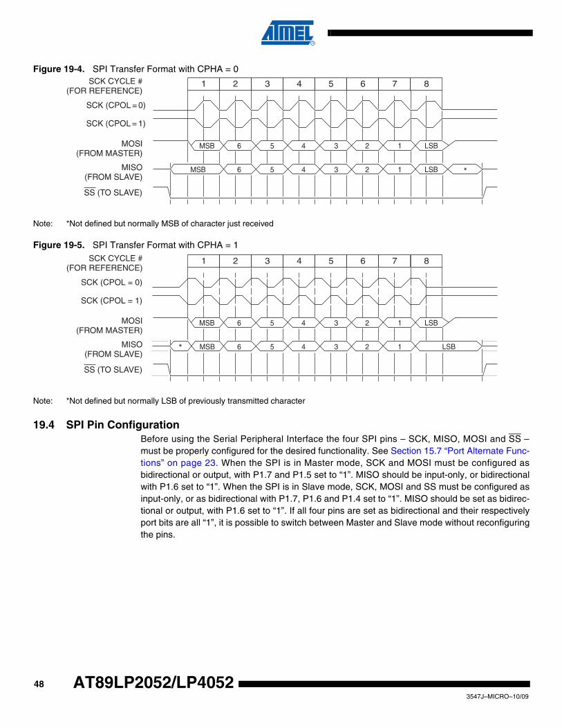
Figure 19-4. SPI Transfer Format with CPHA = 0
Note: *Not defined but normally MSB of character just received
Figure 19-5. SPI Transfer Format with CPHA = 1
Note: *Not defined but normally LSB of previously transmitted character
19.4 SPI Pin ConfigurationBefore using the Serial Peripheral Interface the four SPI pins – SCK, MISO, MOSI and SS –must be properly configured for the desired functionality. See Section 15.7 “Port Alternate Func-tions” on page 23. When the SPI is in Master mode, SCK and MOSI must be configured asbidirectional or output, with P1.7 and P1.5 set to “1”. MISO should be input-only, or bidirectionalwith P1.6 set to “1”. When the SPI is in Slave mode, SCK, MOSI and SS must be configured asinput-only, or as bidirectional with P1.7, P1.6 and P1.4 set to “1”. MISO should be set as bidirec-tional or output, with P1.6 set to “1”. If all four pins are set as bidirectional and their respectivelyport bits are all “1”, it is possible to switch between Master and Slave mode without reconfiguringthe pins.
MSB 6 5 4 3 2 1 LSB
1 2 3 4 5 6 7 8
MSB* 6 5 4 3 2 1 LSB
SCK CYCLE #(FOR REFERENCE)
SCK (CPOL = 0)
SCK (CPOL = 1)
MOSI(FROM MASTER)
MISO(FROM SLAVE)
SS (TO SLAVE)
483547J–MICRO–10/09
AT89LP2052/LP4052
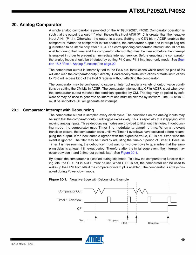
AT89LP2052/LP4052
20. Analog ComparatorA single analog comparator is provided on the AT89LP2052/LP4052. Comparator operation issuch that the output is a logic “1” when the positive input AIN0 (P1.0) is greater than the negativeinput AIN1 (P1.1). Otherwise, the output is a zero. Setting the CEN bit in ACSR enables thecomparator. When the comparator is first enabled, the comparator output and interrupt flag areguaranteed to be stable only after 10 µs. The corresponding comparator interrupt should not beenabled during that time, and the comparator interrupt flag must be cleared before the interruptis enabled in order to prevent an immediate interrupt service. Before enabling the comparatorthe analog inputs should be tri-stated by putting P1.0 and P1.1 into input-only mode. See Sec-tion 15.5 “Port 1 Analog Functions” on page 22.
The comparator output is internally tied to the P3.6 pin. Instructions which read the pins of P3will also read the comparator output directly. Read-Modify-Write instructions or Write instructionsto P3.6 will access bit 6 of the Port 3 register without affecting the comparator.
The comparator may be configured to cause an interrupt under a variety of output value condi-tions by setting the CM bits in ACSR. The comparator interrupt flag CF in ACSR is set wheneverthe comparator output matches the condition specified by CM. The flag may be polled by soft-ware or may be used to generate an interrupt and must be cleared by software. The EC bit in IEmust be set before CF will generate an interrupt.
20.1 Comparator Interrupt with DebouncingThe comparator output is sampled every clock cycle. The conditions on the analog inputs maybe such that the comparator output will toggle excessively. This is especially true if applying slowmoving analog inputs. Three debouncing modes are provided to filter out this noise. In debounc-ing mode, the comparator uses Timer 1 to modulate its sampling time. When a relevanttransition occurs, the comparator waits until two Timer 1 overflows have occurred before resam-pling the output. If the new sample agrees with the expected value, CF is set. Otherwise theevent is ignored. The filter may be tuned by adjusting the time-out period of Timer 1. BecauseTimer 1 is free running, the debouncer must wait for two overflows to guarantee that the sam-pling delay is at least 1 time-out period. Therefore after the initial edge event, the interrupt mayoccur between 1 and 2 time-out periods later. See Figure 20-1.
By default the comparator is disabled during Idle mode. To allow the comparator to function dur-ing Idle, the CIDL bit in ACSR must be set. When CIDL is set, the comparator can be used towake-up the CPU from Idle if the comparator interrupt is enabled. The comparator is always dis-abled during Power-down mode.
Figure 20-1. Negative Edge with Debouncing Example
Comparator Out
Timer 1 Overflow
CF
Start Compare Start Compare
493547J–MICRO–10/09
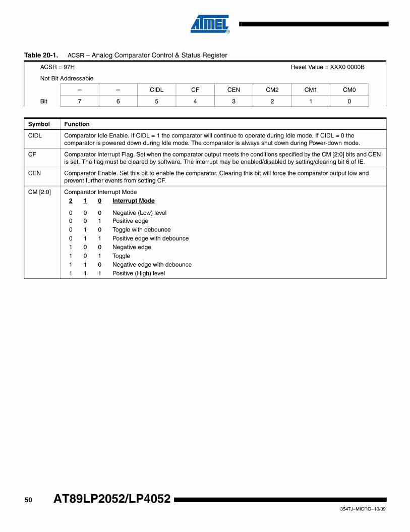
Table 20-1. ACSR – Analog Comparator Control & Status Register
ACSR = 97H Reset Value = XXX0 0000B
Not Bit Addressable
– – CIDL CF CEN CM2 CM1 CM0
Bit 7 6 5 4 3 2 1 0
Symbol Function
CIDL Comparator Idle Enable. If CIDL = 1 the comparator will continue to operate during Idle mode. If CIDL = 0 the comparator is powered down during Idle mode. The comparator is always shut down during Power-down mode.
CF Comparator Interrupt Flag. Set when the comparator output meets the conditions specified by the CM [2:0] bits and CEN is set. The flag must be cleared by software. The interrupt may be enabled/disabled by setting/clearing bit 6 of IE.
CEN Comparator Enable. Set this bit to enable the comparator. Clearing this bit will force the comparator output low and prevent further events from setting CF.
CM [2:0] Comparator Interrupt Mode2 1 0 Interrupt Mode
0 0 0 Negative (Low) level0 0 1 Positive edge
0 1 0 Toggle with debounce
0 1 1 Positive edge with debounce1 0 0 Negative edge
1 0 1 Toggle
1 1 0 Negative edge with debounce1 1 1 Positive (High) level
503547J–MICRO–10/09
AT89LP2052/LP4052
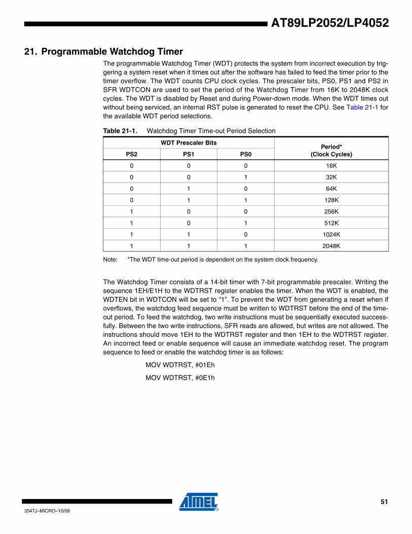
AT89LP2052/LP4052
21. Programmable Watchdog TimerThe programmable Watchdog Timer (WDT) protects the system from incorrect execution by trig-gering a system reset when it times out after the software has failed to feed the timer prior to thetimer overflow. The WDT counts CPU clock cycles. The prescaler bits, PS0, PS1 and PS2 inSFR WDTCON are used to set the period of the Watchdog Timer from 16K to 2048K clockcycles. The WDT is disabled by Reset and during Power-down mode. When the WDT times outwithout being serviced, an internal RST pulse is generated to reset the CPU. See Table 21-1 forthe available WDT period selections.
Note: *The WDT time-out period is dependent on the system clock frequency.
The Watchdog Timer consists of a 14-bit timer with 7-bit programmable prescaler. Writing thesequence 1EH/E1H to the WDTRST register enables the timer. When the WDT is enabled, theWDTEN bit in WDTCON will be set to “1”. To prevent the WDT from generating a reset when ifoverflows, the watchdog feed sequence must be written to WDTRST before the end of the time-out period. To feed the watchdog, two write instructions must be sequentially executed success-fully. Between the two write instructions, SFR reads are allowed, but writes are not allowed. Theinstructions should move 1EH to the WDTRST register and then 1EH to the WDTRST register.An incorrect feed or enable sequence will cause an immediate watchdog reset. The programsequence to feed or enable the watchdog timer is as follows:
MOV WDTRST, #01Eh
MOV WDTRST, #0E1h
Table 21-1. Watchdog Timer Time-out Period Selection
WDT Prescaler BitsPeriod*
(Clock Cycles)PS2 PS1 PS0
0 0 0 16K
0 0 1 32K
0 1 0 64K
0 1 1 128K
1 0 0 256K
1 0 1 512K
1 1 0 1024K
1 1 1 2048K
513547J–MICRO–10/09
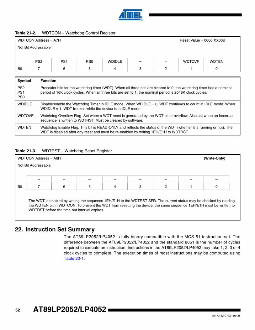
S
22. Instruction Set SummaryThe AT89LP2052/LP4052 is fully binary compatible with the MCS-51 instruction set. Thedifference between the AT89LP2052/LP4052 and the standard 8051 is the number of cyclesrequired to execute an instruction. Instructions in the AT89LP2052/LP4052 may take 1, 2, 3 or 4clock cycles to complete. The execution times of most instructions may be computed usingTable 22-1.
Table 21-2. WDTCON – Watchdog Control Register
WDTCON Address = A7H Reset Value = 0000 XX00B
Not Bit Addressable
PS2 PS1 PS0 WDIDLE – – WDTOVF WDTEN
Bit 7 6 5 4 3 2 1 0
Symbol Function
PS2PS1PS0
Prescaler bits for the watchdog timer (WDT). When all three bits are cleared to 0, the watchdog timer has a nominal period of 16K clock cycles. When all three bits are set to 1, the nominal period is 2048K clock cycles.
WDIDLE Disable/enable the Watchdog Timer in IDLE mode. When WDIDLE = 0, WDT continues to count in IDLE mode. When WDIDLE = 1, WDT freezes while the device is in IDLE mode.
WDTOVF Watchdog Overflow Flag. Set when a WDT reset is generated by the WDT timer overflow. Also set when an incorrect sequence is written to WDTRST. Must be cleared by software.
WDTEN Watchdog Enable Flag. This bit is READ-ONLY and reflects the status of the WDT (whether it is running or not). The WDT is disabled after any reset and must be re-enabled by writing 1EH/E1H to WDTRST
Table 21-3. WDTRST – Watchdog Reset Register
WDTCON Address = A6H (Write-Only)
Not Bit Addressable
– – – – – – – –
Bit 7 6 5 4 3 2 1 0
The WDT is enabled by writing the sequence 1EH/E1H to the WDTRST SFR. The current status may be checked by reading the WDTEN bit in WDTCON. To prevent the WDT from resetting the device, the same sequence 1EH/E1H must be written to WDTRST before the time-out interval expires.
523547J–MICRO–10/09
AT89LP2052/LP4052
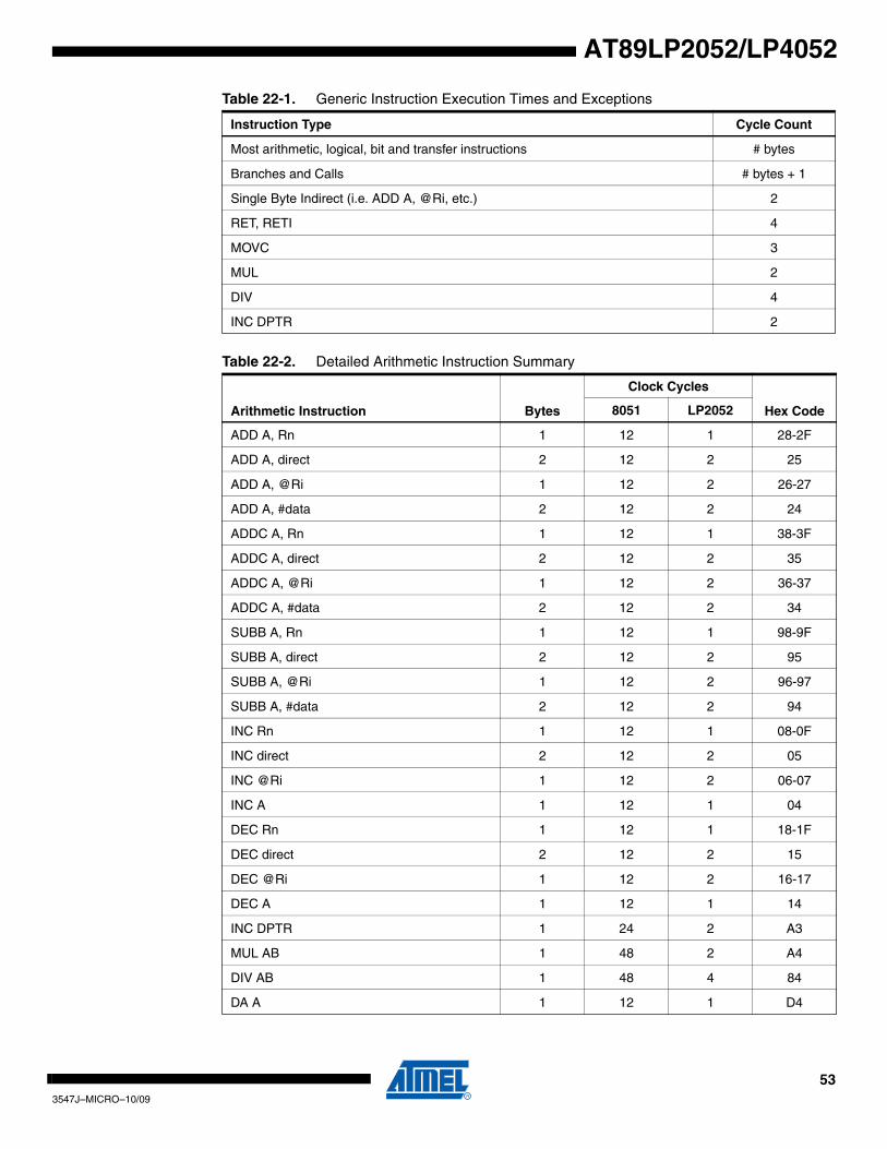
AT89LP2052/LP4052
Table 22-1. Generic Instruction Execution Times and Exceptions
Instruction Type Cycle Count
Most arithmetic, logical, bit and transfer instructions # bytes
Branches and Calls # bytes + 1
Single Byte Indirect (i.e. ADD A, @Ri, etc.) 2
RET, RETI 4
MOVC 3
MUL 2
DIV 4
INC DPTR 2
Table 22-2. Detailed Arithmetic Instruction Summary
Arithmetic Instruction Bytes
Clock Cycles
Hex Code8051 LP2052
ADD A, Rn 1 12 1 28-2F
ADD A, direct 2 12 2 25
ADD A, @Ri 1 12 2 26-27
ADD A, #data 2 12 2 24
ADDC A, Rn 1 12 1 38-3F
ADDC A, direct 2 12 2 35
ADDC A, @Ri 1 12 2 36-37
ADDC A, #data 2 12 2 34
SUBB A, Rn 1 12 1 98-9F
SUBB A, direct 2 12 2 95
SUBB A, @Ri 1 12 2 96-97
SUBB A, #data 2 12 2 94
INC Rn 1 12 1 08-0F
INC direct 2 12 2 05
INC @Ri 1 12 2 06-07
INC A 1 12 1 04
DEC Rn 1 12 1 18-1F
DEC direct 2 12 2 15
DEC @Ri 1 12 2 16-17
DEC A 1 12 1 14
INC DPTR 1 24 2 A3
MUL AB 1 48 2 A4
DIV AB 1 48 4 84
DA A 1 12 1 D4
533547J–MICRO–10/09
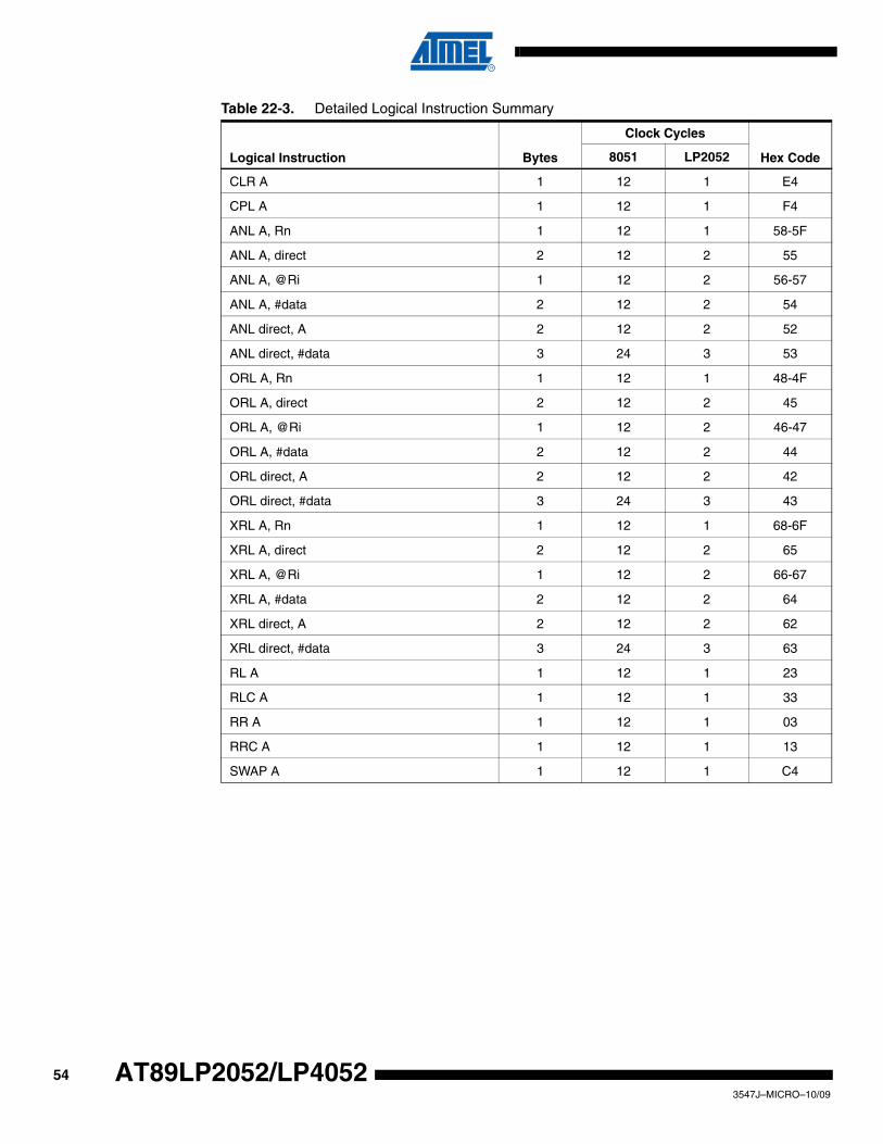
Table 22-3. Detailed Logical Instruction Summary
Logical Instruction Bytes
Clock Cycles
Hex Code8051 LP2052
CLR A 1 12 1 E4
CPL A 1 12 1 F4
ANL A, Rn 1 12 1 58-5F
ANL A, direct 2 12 2 55
ANL A, @Ri 1 12 2 56-57
ANL A, #data 2 12 2 54
ANL direct, A 2 12 2 52
ANL direct, #data 3 24 3 53
ORL A, Rn 1 12 1 48-4F
ORL A, direct 2 12 2 45
ORL A, @Ri 1 12 2 46-47
ORL A, #data 2 12 2 44
ORL direct, A 2 12 2 42
ORL direct, #data 3 24 3 43
XRL A, Rn 1 12 1 68-6F
XRL A, direct 2 12 2 65
XRL A, @Ri 1 12 2 66-67
XRL A, #data 2 12 2 64
XRL direct, A 2 12 2 62
XRL direct, #data 3 24 3 63
RL A 1 12 1 23
RLC A 1 12 1 33
RR A 1 12 1 03
RRC A 1 12 1 13
SWAP A 1 12 1 C4
543547J–MICRO–10/09
AT89LP2052/LP4052
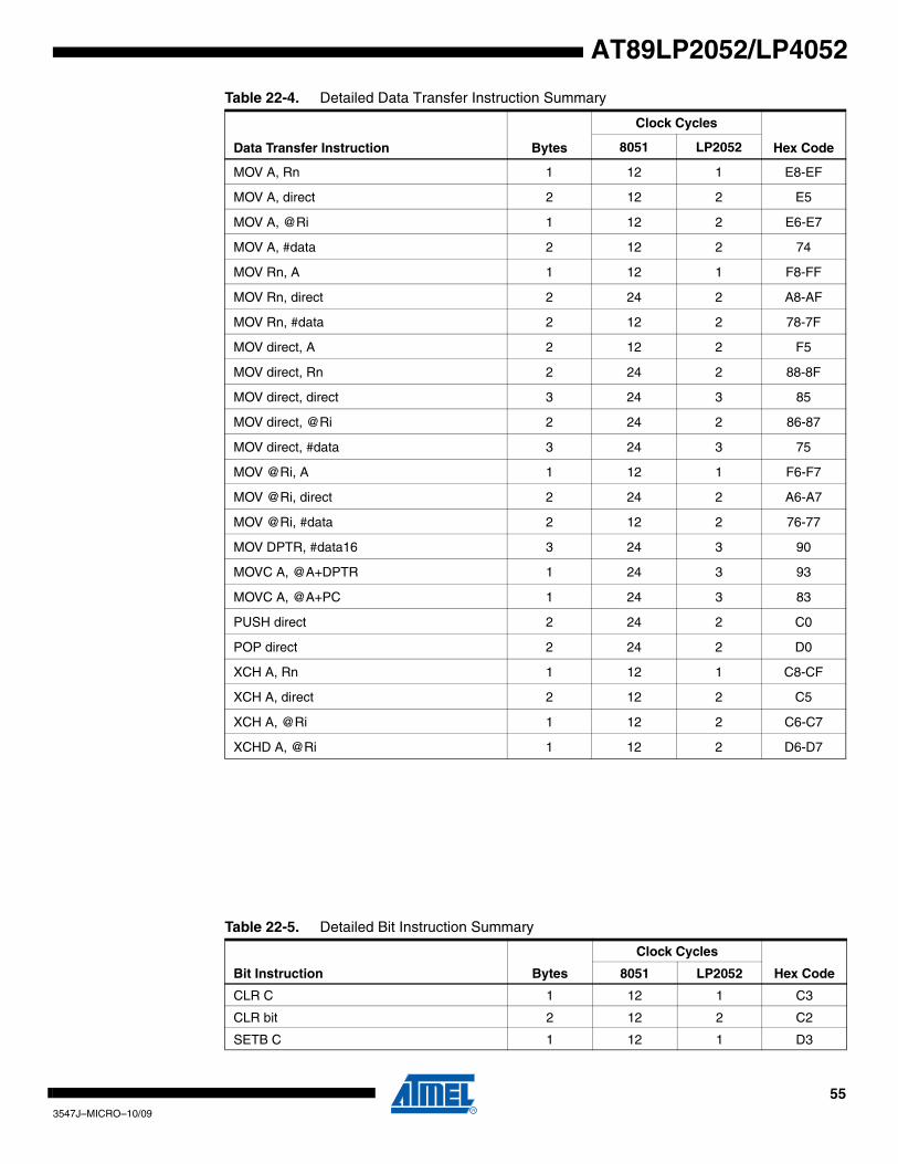
AT89LP2052/LP4052
Table 22-4. Detailed Data Transfer Instruction Summary
Data Transfer Instruction Bytes
Clock Cycles
Hex Code8051 LP2052
MOV A, Rn 1 12 1 E8-EF
MOV A, direct 2 12 2 E5
MOV A, @Ri 1 12 2 E6-E7
MOV A, #data 2 12 2 74
MOV Rn, A 1 12 1 F8-FF
MOV Rn, direct 2 24 2 A8-AF
MOV Rn, #data 2 12 2 78-7F
MOV direct, A 2 12 2 F5
MOV direct, Rn 2 24 2 88-8F
MOV direct, direct 3 24 3 85
MOV direct, @Ri 2 24 2 86-87
MOV direct, #data 3 24 3 75
MOV @Ri, A 1 12 1 F6-F7
MOV @Ri, direct 2 24 2 A6-A7
MOV @Ri, #data 2 12 2 76-77
MOV DPTR, #data16 3 24 3 90
MOVC A, @A+DPTR 1 24 3 93
MOVC A, @A+PC 1 24 3 83
PUSH direct 2 24 2 C0
POP direct 2 24 2 D0
XCH A, Rn 1 12 1 C8-CF
XCH A, direct 2 12 2 C5
XCH A, @Ri 1 12 2 C6-C7
XCHD A, @Ri 1 12 2 D6-D7
Table 22-5. Detailed Bit Instruction Summary
Bit Instruction Bytes
Clock Cycles
Hex Code8051 LP2052
CLR C 1 12 1 C3
CLR bit 2 12 2 C2
SETB C 1 12 1 D3
553547J–MICRO–10/09
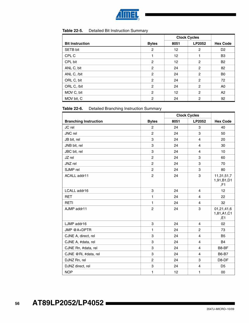
SETB bit 2 12 2 D2
CPL C 1 12 1 B3
CPL bit 2 12 2 B2
ANL C, bit 2 24 2 82
ANL C, /bit 2 24 2 B0
ORL C, bit 2 24 2 72
ORL C, /bit 2 24 2 A0
MOV C, bit 2 12 2 A2
MOV bit, C 2 24 2 92
Table 22-6. Detailed Branching Instruction Summary
Branching Instruction Bytes
Clock Cycles
Hex Code8051 LP2052
JC rel 2 24 3 40
JNC rel 2 24 3 50
JB bit, rel 3 24 4 20
JNB bit, rel 3 24 4 30
JBC bit, rel 3 24 4 10
JZ rel 2 24 3 60
JNZ rel 2 24 3 70
SJMP rel 2 24 3 80
ACALL addr11 2 24 3 11,31,51,71,91,B1,D1
,F1
LCALL addr16 3 24 4 12
RET 1 24 4 22
RETI 1 24 4 32
AJMP addr11 2 24 3 01,21,41,61,81,A1,C1
,E1
LJMP addr16 3 24 4 02
JMP @A+DPTR 1 24 2 73
CJNE A, direct, rel 3 24 4 B5
CJNE A, #data, rel 3 24 4 B4
CJNE Rn, #data, rel 3 24 4 B8-BF
CJNE @Ri, #data, rel 3 24 4 B6-B7
DJNZ Rn, rel 2 24 3 D8-DF
DJNZ direct, rel 3 24 4 D5
NOP 1 12 1 00
Table 22-5. Detailed Bit Instruction Summary
Bit Instruction Bytes
Clock Cycles
Hex Code8051 LP2052
563547J–MICRO–10/09
AT89LP2052/LP4052
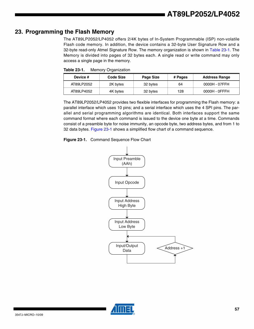
AT89LP2052/LP4052
23. Programming the Flash MemoryThe AT89LP2052/LP4052 offers 2/4K bytes of In-System Programmable (ISP) non-volatileFlash code memory. In addition, the device contains a 32-byte User Signature Row and a32-byte read-only Atmel Signature Row. The memory organization is shown in Table 23-1. TheMemory is divided into pages of 32 bytes each. A single read or write command may onlyaccess a single page in the memory.
The AT89LP2052/LP4052 provides two flexible interfaces for programming the Flash memory: aparallel interface which uses 10 pins; and a serial interface which uses the 4 SPI pins. The par-allel and serial programming algorithms are identical. Both interfaces support the samecommand format where each command is issued to the device one byte at a time. Commandsconsist of a preamble byte for noise immunity, an opcode byte, two address bytes, and from 1 to32 data bytes. Figure 23-1 shows a simplified flow chart of a command sequence.
Figure 23-1. Command Sequence Flow Chart
Table 23-1. Memory Organization
Device # Code Size Page Size # Pages Address Range
AT89LP2052 2K bytes 32 bytes 64 0000H - 07FFH
AT89LP4052 4K bytes 32 bytes 128 0000H - 0FFFH
Input Preamble(AAh)
Input Opcode
Input AddressHigh Byte
Input AddressLow Byte
Input/OutputData
Address +1
573547J–MICRO–10/09
Notes: 1. Program Enable must be the first command issued after entering into programming mode.2. Any number of Data bytes from 1 to 32 may be written/read. The internal address is incremented between each byte.3. Fuse Bit Definitions:
*The AT89LP2052/LP4052 has ISP enabled by default from the factory. However, if ISP is later disabled, the ISP EnableFuse must be enabled by using Parallel Programming before entering ISP mode. When disabling the ISP fuse during ISP, the current ISP session will remain active until RST is brought low.
4. Lock Bit Definitions:
5. Atmel Signature Byte:
6. Symbol Key:
23.1 Programming Command Summary
Command Preamble Opcode Addr High Addr Low Data 0 Data n
Program Enable(1) 1010 1010 1010 1100 0101 0011
Chip Erase 1010 1010 1000 1010
Read Status 1010 1010 0110 0000 xxxx xxxx xxxx xxxx Status Out
Load Code Page Buffer(2) 1010 1010 0101 0001 xxxx xxxx xxxB BBBB DataIn 0 ... DataIn n
Write Code Page(2) 1010 1010 0101 0000 xxxx AAAA AAAB BBBB DataIn 0 ... DataIn n
Read Code Page(2) 1010 1010 0011 0000 xxxx AAAA AAAB BBBB DataOut 0 ... DataOut n
Write User Fuses(3) 1010 1010 1110 0001 xxxx xxxx xxxx xxxx xxxx FFFF
Read User Fuses(3) 1010 1010 0110 0001 xxxx xxxx xxxx xxxx xxxx FFFF
Write Lock Bits(4) 1010 1010 1110 0100 xxxx xxxx xxxx xxxx xxxx xxLL
Read Lock Bits(4) 1010 1010 0110 0100 xxxx xxxx xxxx xxxx xxxx xxLL
Write User Signature Page(2) 1010 1010 0101 0010 xxxx xxxx xxxB BBBB DataIn 0 ... DataIn n
Read User Signature Page(2) 1010 1010 0011 0010 xxxx xxxx xxxB BBBB DataOut 0 ... DataOut n
Read Atmel Signature Page(2)(5) 1010 1010 0011 1000 xxxx xxxx xxxB BBBB DataOut 0 ... DataOut n
Bit 0
Bit 1
Bit 2
Bit 3
ISP Enable*
XTAL Osc Bypass
User Row Programming
System Clock Out
Enable = 0/Disable = 1
Enable = 0/Disable = 1
Enable = 0/Disable = 1
Enable = 0/Disable = 1
Bit 0
Bit 1
Lock Bit 1
Lock Bit 2
Locked = 0/Unlocked = 1
Locked = 0/Unlocked = 1
AT89LP2052: Address 00H = 1EH
01H = 25H
02H = FFH
AT89LP4052: Address 00H = 1EH
01H = 45H
02H = FFH
A: Page Address Bit
B: Byte Address Bit
F: Fuse Bit Data
L: Lock Bit Data
x: Don’t Care
583547J–MICRO–10/09
AT89LP2052/LP4052
AT89LP2052/LP4052
23.2 Status RegisterThe current state of the memory may be accessed by reading the status register. The status reg-ister is shown in Table 23-2.
23.3 DATA PollingThe AT89LP2052/LP4052 implements DATA polling to indicate the end of a programming cycle.While the device is busy, any attempted read of the last byte written will return the data byte withthe MSB complemented. Once the programming cycle has completed, the true value will beaccessible. During Erase the data is assumed to be FFH and DATA polling will return 7FH.When writing multiple bytes in a page, the DATA value will be the last data byte loaded beforeprogramming begins, not the written byte with the highest physical address within the page.
23.4 Parallel ProgrammingParallel Programming Mode is enabled by applying VPP to the RST pin. The connectionsrequired during parallel mode are shown in Figure 23-2. During parallel programming, Port 1 isconfigured as an 8-bit wide bidirectional command bus. Data on P1 is strobed by a positivepulse on the XTAL1 pin. No other clock is required. The interface is enabled by pulling CS (P3.2)low. P3.1 acts as RDY/BSY, and will be pulled low to indicate that the device is busy regardlessof the state of CS.
Table 23-2. Status Register
– – – – LOAD SUCCESS WRTINH BUSY
Bit 7 6 5 4 3 2 1 0
Symbol Function
LOADLoad flag. Cleared low by the load page buffer command and set high by the next memory write. This flag signals that the page buffer was previously loaded with data by the load page buffer command.
SUCCESSSuccess flag. Cleared low at the start of a programming cycle and will only be set high if the programming cycle completes without interruption from the brownout detector.
WRTINHWrite Inhibit flag. Cleared low by the brownout detector (BOD) whenever programming is inhibited due to VCC falling below the minimum required programming voltage. If a BOD episode occurs during programming, the SUCCESS flag will remain low after the cycle is complete. WRTINH low also forces BUSY low.
BUSY Busy flag. Cleared low whenever the memory is busy programming or if write is currently inhibited.
593547J–MICRO–10/09
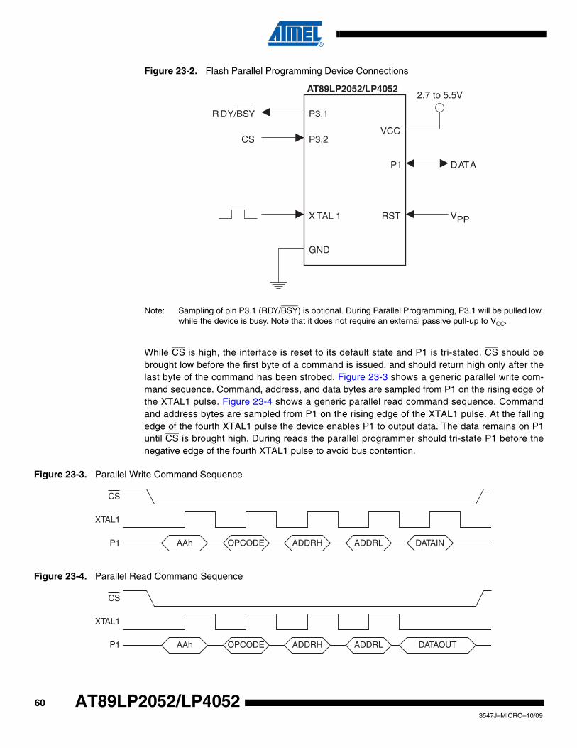
Figure 23-2. Flash Parallel Programming Device Connections
Note: Sampling of pin P3.1 (RDY/BSY) is optional. During Parallel Programming, P3.1 will be pulled low while the device is busy. Note that it does not require an external passive pull-up to VCC.
While CS is high, the interface is reset to its default state and P1 is tri-stated. CS should bebrought low before the first byte of a command is issued, and should return high only after thelast byte of the command has been strobed. Figure 23-3 shows a generic parallel write com-mand sequence. Command, address, and data bytes are sampled from P1 on the rising edge ofthe XTAL1 pulse. Figure 23-4 shows a generic parallel read command sequence. Commandand address bytes are sampled from P1 on the rising edge of the XTAL1 pulse. At the fallingedge of the fourth XTAL1 pulse the device enables P1 to output data. The data remains on P1until CS is brought high. During reads the parallel programmer should tri-state P1 before thenegative edge of the fourth XTAL1 pulse to avoid bus contention.
Figure 23-3. Parallel Write Command Sequence
Figure 23-4. Parallel Read Command Sequence
AT89LP2052/LP4052
VCC
P1
RST
P3.1
XTAL 1
P3.2
GND
2.7 to 5.5V
R DY/BSY
CS
VPP
DATA
AAh OPCODE ADDRH ADDRL DATAIN
CS
XTAL1
P1
AAh OPCODE ADDRH ADDRL DATAOUT
CS
XTAL1
P1
603547J–MICRO–10/09
AT89LP2052/LP4052
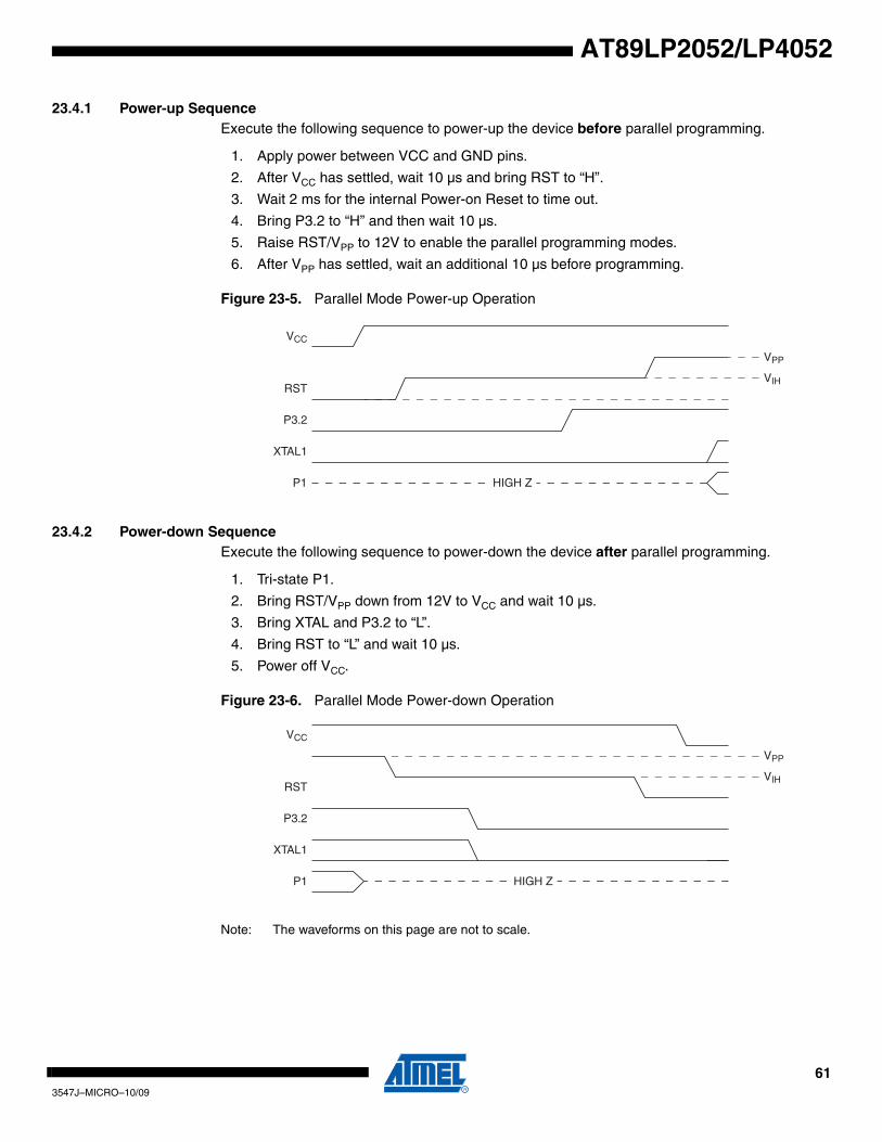
AT89LP2052/LP4052
23.4.1 Power-up Sequence Execute the following sequence to power-up the device before parallel programming.
1. Apply power between VCC and GND pins.
2. After VCC has settled, wait 10 µs and bring RST to “H”.
3. Wait 2 ms for the internal Power-on Reset to time out.
4. Bring P3.2 to “H” and then wait 10 µs.
5. Raise RST/VPP to 12V to enable the parallel programming modes.
6. After VPP has settled, wait an additional 10 µs before programming.
Figure 23-5. Parallel Mode Power-up Operation
23.4.2 Power-down Sequence Execute the following sequence to power-down the device after parallel programming.
1. Tri-state P1.
2. Bring RST/VPP down from 12V to VCC and wait 10 µs.
3. Bring XTAL and P3.2 to “L”.
4. Bring RST to “L” and wait 10 µs.
5. Power off VCC.
Figure 23-6. Parallel Mode Power-down Operation
Note: The waveforms on this page are not to scale.
VCC
RSTVIH
VPP
P3.2
XTAL1
HIGH ZP1
VCC
RSTVIH
VPP
P3.2
XTAL1
HIGH ZP1
613547J–MICRO–10/09
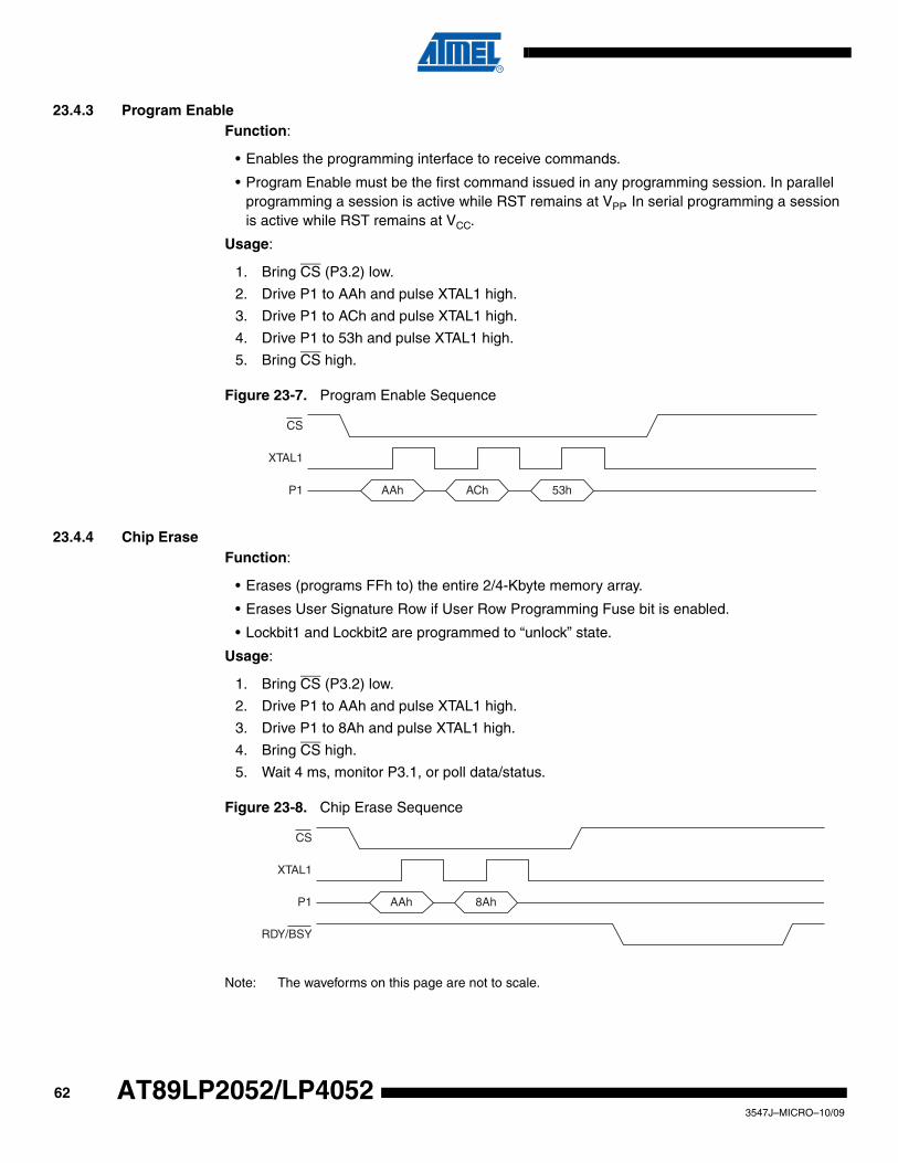
23.4.3 Program EnableFunction:
• Enables the programming interface to receive commands.
• Program Enable must be the first command issued in any programming session. In parallel programming a session is active while RST remains at VPP. In serial programming a session is active while RST remains at VCC.
Usage:
1. Bring CS (P3.2) low.
2. Drive P1 to AAh and pulse XTAL1 high.
3. Drive P1 to ACh and pulse XTAL1 high.
4. Drive P1 to 53h and pulse XTAL1 high.
5. Bring CS high.
Figure 23-7. Program Enable Sequence
23.4.4 Chip EraseFunction:
• Erases (programs FFh to) the entire 2/4-Kbyte memory array.
• Erases User Signature Row if User Row Programming Fuse bit is enabled.
• Lockbit1 and Lockbit2 are programmed to “unlock” state.
Usage:
1. Bring CS (P3.2) low.
2. Drive P1 to AAh and pulse XTAL1 high.
3. Drive P1 to 8Ah and pulse XTAL1 high.
4. Bring CS high.
5. Wait 4 ms, monitor P3.1, or poll data/status.
Figure 23-8. Chip Erase Sequence
Note: The waveforms on this page are not to scale.
AAh ACh 53h
CS
XTAL1
P1
AAh 8Ah
CS
XTAL1
P1
RDY/BSY
623547J–MICRO–10/09
AT89LP2052/LP4052
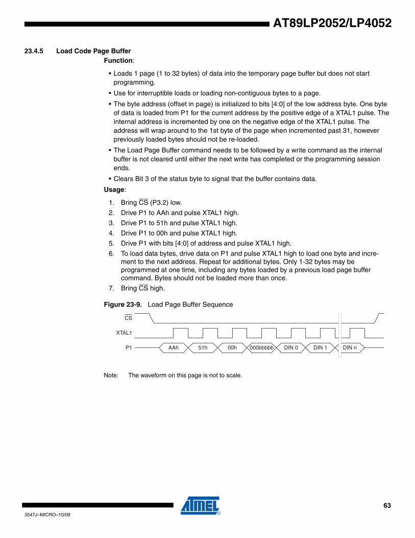
AT89LP2052/LP4052
23.4.5 Load Code Page BufferFunction:
• Loads 1 page (1 to 32 bytes) of data into the temporary page buffer but does not start programming.
• Use for interruptible loads or loading non-contiguous bytes to a page.
• The byte address (offset in page) is initialized to bits [4:0] of the low address byte. One byte of data is loaded from P1 for the current address by the positive edge of a XTAL1 pulse. The internal address is incremented by one on the negative edge of the XTAL1 pulse. The address will wrap around to the 1st byte of the page when incremented past 31, however previously loaded bytes should not be re-loaded.
• The Load Page Buffer command needs to be followed by a write command as the internal buffer is not cleared until either the next write has completed or the programming session ends.
• Clears Bit 3 of the status byte to signal that the buffer contains data.
Usage:
1. Bring CS (P3.2) low.
2. Drive P1 to AAh and pulse XTAL1 high.
3. Drive P1 to 51h and pulse XTAL1 high.
4. Drive P1 to 00h and pulse XTAL1 high.
5. Drive P1 with bits [4:0] of address and pulse XTAL1 high.
6. To load data bytes, drive data on P1 and pulse XTAL1 high to load one byte and incre-ment to the next address. Repeat for additional bytes. Only 1-32 bytes may be programmed at one time, including any bytes loaded by a previous load page buffer command. Bytes should not be loaded more than once.
7. Bring CS high.
Figure 23-9. Load Page Buffer Sequence
Note: The waveform on this page is not to scale.
AAh 51h 00h 000bbbbb DIN 0
CS
XTAL1
P1 DIN 1 DIN n
633547J–MICRO–10/09
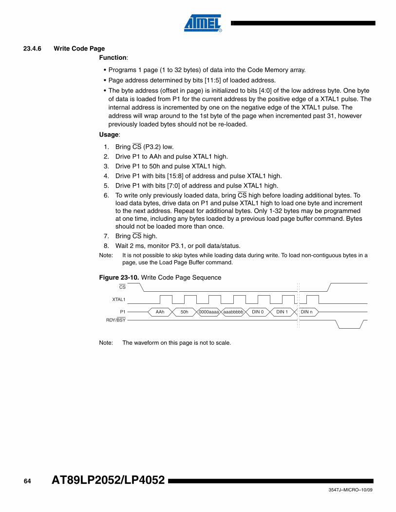
23.4.6 Write Code PageFunction:
• Programs 1 page (1 to 32 bytes) of data into the Code Memory array.
• Page address determined by bits [11:5] of loaded address.
• The byte address (offset in page) is initialized to bits [4:0] of the low address byte. One byte of data is loaded from P1 for the current address by the positive edge of a XTAL1 pulse. The internal address is incremented by one on the negative edge of the XTAL1 pulse. The address will wrap around to the 1st byte of the page when incremented past 31, however previously loaded bytes should not be re-loaded.
Usage:
1. Bring CS (P3.2) low.
2. Drive P1 to AAh and pulse XTAL1 high.
3. Drive P1 to 50h and pulse XTAL1 high.
4. Drive P1 with bits [15:8] of address and pulse XTAL1 high.
5. Drive P1 with bits [7:0] of address and pulse XTAL1 high.
6. To write only previously loaded data, bring CS high before loading additional bytes. To load data bytes, drive data on P1 and pulse XTAL1 high to load one byte and increment to the next address. Repeat for additional bytes. Only 1-32 bytes may be programmed at one time, including any bytes loaded by a previous load page buffer command. Bytes should not be loaded more than once.
7. Bring CS high.
8. Wait 2 ms, monitor P3.1, or poll data/status. Note: It is not possible to skip bytes while loading data during write. To load non-contiguous bytes in a
page, use the Load Page Buffer command.
Figure 23-10. Write Code Page Sequence
Note: The waveform on this page is not to scale.
AAh 50h 0000aaaa aaabbbbb DIN 0
CS
XTAL1
P1 DIN 1 DIN n
RDY/BSY
643547J–MICRO–10/09
AT89LP2052/LP4052
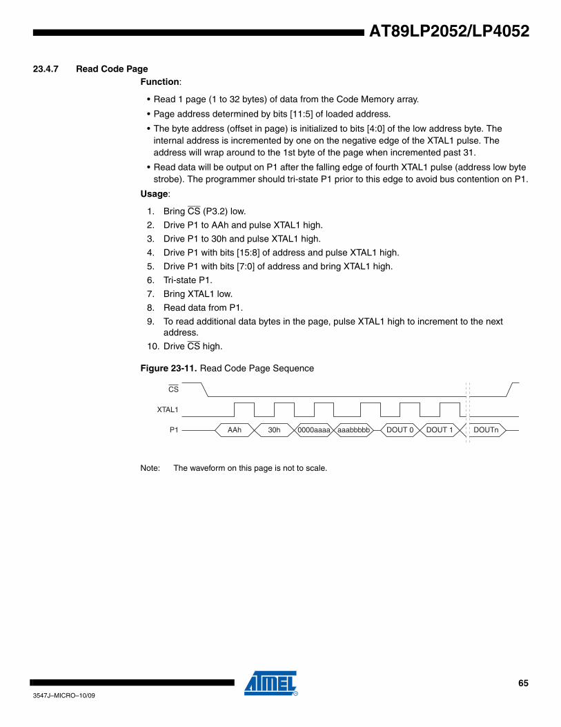
AT89LP2052/LP4052
23.4.7 Read Code PageFunction:
• Read 1 page (1 to 32 bytes) of data from the Code Memory array.
• Page address determined by bits [11:5] of loaded address.
• The byte address (offset in page) is initialized to bits [4:0] of the low address byte. The internal address is incremented by one on the negative edge of the XTAL1 pulse. The address will wrap around to the 1st byte of the page when incremented past 31.
• Read data will be output on P1 after the falling edge of fourth XTAL1 pulse (address low byte strobe). The programmer should tri-state P1 prior to this edge to avoid bus contention on P1.
Usage:
1. Bring CS (P3.2) low.
2. Drive P1 to AAh and pulse XTAL1 high.
3. Drive P1 to 30h and pulse XTAL1 high.
4. Drive P1 with bits [15:8] of address and pulse XTAL1 high.
5. Drive P1 with bits [7:0] of address and bring XTAL1 high.
6. Tri-state P1.
7. Bring XTAL1 low.
8. Read data from P1.
9. To read additional data bytes in the page, pulse XTAL1 high to increment to the next address.
10. Drive CS high.
Figure 23-11. Read Code Page Sequence
Note: The waveform on this page is not to scale.
AAh 30h 0000aaaa aaabbbbb DOUT 0
CS
XTAL1
P1 DOUT 1 DOUTn
653547J–MICRO–10/09
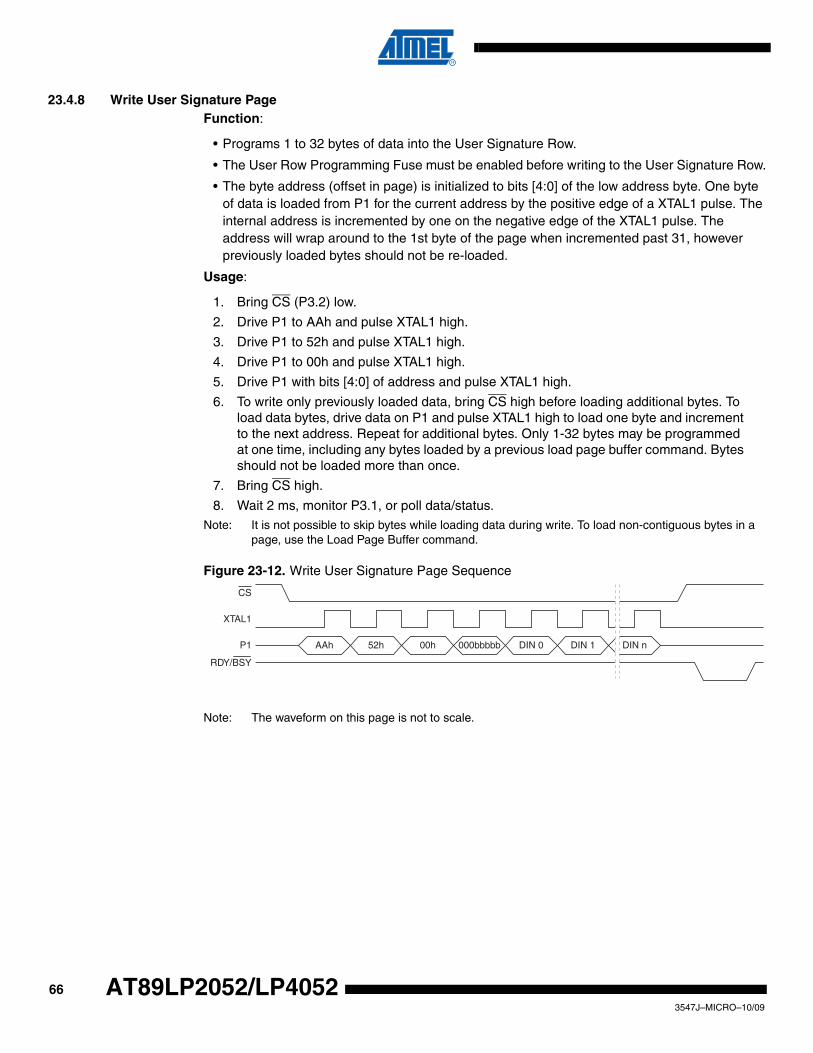
23.4.8 Write User Signature PageFunction:
• Programs 1 to 32 bytes of data into the User Signature Row.
• The User Row Programming Fuse must be enabled before writing to the User Signature Row.
• The byte address (offset in page) is initialized to bits [4:0] of the low address byte. One byte of data is loaded from P1 for the current address by the positive edge of a XTAL1 pulse. The internal address is incremented by one on the negative edge of the XTAL1 pulse. The address will wrap around to the 1st byte of the page when incremented past 31, however previously loaded bytes should not be re-loaded.
Usage:
1. Bring CS (P3.2) low.
2. Drive P1 to AAh and pulse XTAL1 high.
3. Drive P1 to 52h and pulse XTAL1 high.
4. Drive P1 to 00h and pulse XTAL1 high.
5. Drive P1 with bits [4:0] of address and pulse XTAL1 high.
6. To write only previously loaded data, bring CS high before loading additional bytes. To load data bytes, drive data on P1 and pulse XTAL1 high to load one byte and increment to the next address. Repeat for additional bytes. Only 1-32 bytes may be programmed at one time, including any bytes loaded by a previous load page buffer command. Bytes should not be loaded more than once.
7. Bring CS high.
8. Wait 2 ms, monitor P3.1, or poll data/status. Note: It is not possible to skip bytes while loading data during write. To load non-contiguous bytes in a
page, use the Load Page Buffer command.
Figure 23-12. Write User Signature Page Sequence
Note: The waveform on this page is not to scale.
AAh 52h 00h 000bbbbb DIN 0
CS
XTAL1
P1 DIN 1 DIN n
RDY/BSY
663547J–MICRO–10/09
AT89LP2052/LP4052
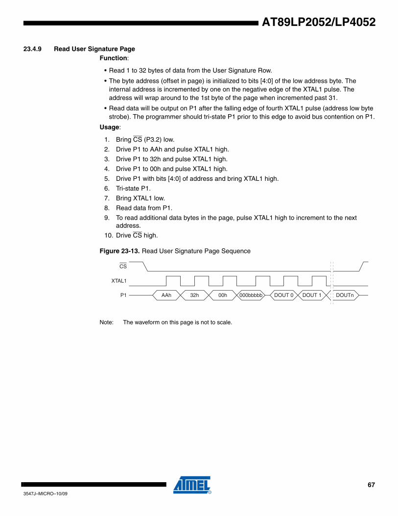
AT89LP2052/LP4052
23.4.9 Read User Signature PageFunction:
• Read 1 to 32 bytes of data from the User Signature Row.
• The byte address (offset in page) is initialized to bits [4:0] of the low address byte. The internal address is incremented by one on the negative edge of the XTAL1 pulse. The address will wrap around to the 1st byte of the page when incremented past 31.
• Read data will be output on P1 after the falling edge of fourth XTAL1 pulse (address low byte strobe). The programmer should tri-state P1 prior to this edge to avoid bus contention on P1.
Usage:
1. Bring CS (P3.2) low.
2. Drive P1 to AAh and pulse XTAL1 high.
3. Drive P1 to 32h and pulse XTAL1 high.
4. Drive P1 to 00h and pulse XTAL1 high.
5. Drive P1 with bits [4:0] of address and bring XTAL1 high.
6. Tri-state P1.
7. Bring XTAL1 low.
8. Read data from P1.
9. To read additional data bytes in the page, pulse XTAL1 high to increment to the next address.
10. Drive CS high.
Figure 23-13. Read User Signature Page Sequence
Note: The waveform on this page is not to scale.
AAh 32h 00h 000bbbbb DOUT 0
CS
XTAL1
P1 DOUT 1 DOUTn
673547J–MICRO–10/09
23.4.10 Read Atmel Signature PageFunction:
• Read 1 to 32 bytes of data from the Atmel Signature Row.
• The byte address (offset in page) is initialized to bits [4:0] of the low address byte. The internal address is incremented by one on the negative edge of the XTAL1 pulse. The address will wrap around to the 1st byte of the page when incremented past 31.
• Read data will be output on P1 after the falling edge of fourth XTAL1 pulse (address low byte strobe). The programmer should tri-state P1 prior to this edge to avoid bus contention on P1.
Usage:
1. Bring CS (P3.2) low.
2. Drive P1 to AAh and pulse XTAL1 high.
3. Drive P1 to 38h and pulse XTAL1 high.
4. Drive P1 to 00h and pulse XTAL1 high.
5. Drive P1 with bits [4:0] of address and bring XTAL1 high.
6. Tri-state P1.
7. Bring XTAL1 low.
8. Read data from P1.
9. To read additional data bytes in the page, pulse XTAL1 high to increment to the next address.
10. Drive CS high.
Figure 23-14. Read Atmel Signature Page Sequence
Note: The waveform on this page is not to scale.
AAh 38h 00h 000bbbbb DOUT 0
CS
XTAL1
P1 DOUT 1 DOUTn
683547J–MICRO–10/09
AT89LP2052/LP4052
AT89LP2052/LP4052
23.4.11 Write Lock BitsFunction:
• Program (lock) Lock Bits 1 and 2.
Usage:
1. Bring CS (P3.2) low.
2. Drive P1 to AAh and pulse XTAL1 high.
3. Drive P1 to E4h and pulse XTAL1 high.
4. Drive P1 to 00h and pulse XTAL1 high.
5. Drive P1 to 00h and pulse XTAL1 high.
6. Drive data on P1 and pulse XTAL1 high.
7. Drive CS high.
8. Wait 4 ms, monitor P3.1, or poll data/status.
Figure 23-15. Write Lock Bits Sequence
23.4.12 Read Lock BitsFunction:
• Read status of Lock Bits 1 and 2.
Usage:
1. Bring CS (P3.2) low.
2. Drive P1 to 0xAA and pulse XTAL1 high.
3. Drive P1 to 0x64 and pulse XTAL1 high.
4. Drive P1 to 0x00 and pulse XTAL1 high.
5. Drive P1 to 0x00 and bring XTAL1 high.
6. Tri-state P1.
7. Bring XTAL1 low.
8. Read data from P1.
9. Drive CS high.
Figure 23-16. Read Lock Bits Sequence
Note: The waveforms on this page are not to scale.
AAh E4h 00h 00h 111111LL
CS
XTAL1
P1
RDY/BSY
AAh 64h 00h 00h 111111LL
CS
XTAL1
P1
693547J–MICRO–10/09
23.4.13 Write User FusesFunction:
• Program User Fuses.
• Unimplemented bits should always be written with 1s.
Usage:
1. Bring CS (P3.2) low.
2. Drive P1 to AAh and pulse XTAL1 high.
3. Drive P1 to E1h and pulse XTAL1 high.
4. Drive P1 to 00h and pulse XTAL1 high.
5. Drive P1 to 00h and pulse XTAL1 high.
6. Drive data on P1 and pulse XTAL1 high.
7. Drive CS high.
8. Wait 4 ms, monitor P3.1, or poll data/status.
Figure 23-17. Write User Fuses Sequence
23.4.14 Read User FusesFunction:
• Read status of User Fuses
Usage:
1. Bring CS (P3.2) low.
2. Drive P1 to 0xAA and pulse XTAL1 high.
3. Drive P1 to 0x61 and pulse XTAL1 high.
4. Drive P1 to 0x00 and pulse XTAL1 high.
5. Drive P1 to 0x00 and bring XTAL1 high.
6. Tri-state P1.
7. Bring XTAL1 low.
8. Read data from P1.
9. Drive CS high.
Figure 23-18. Read User Fuses Sequence
Note: The waveforms on this page are not to scale.
AAh E1h 00h 00h 1111FFFF
CS
XTAL1
P1
RDY/BSY
AAh 61h 00h 00h 1111FFFF
CS
XTAL1
P1
703547J–MICRO–10/09
AT89LP2052/LP4052
AT89LP2052/LP4052
23.4.15 Read StatusFunction:
• Read memory status byte.
Usage:
1. Bring CS (P3.2) low.
2. Drive P1 to 0xAA and pulse XTAL1 high.
3. Drive P1 to 0x60 and pulse XTAL1 high.
4. Drive P1 to 0x00 and pulse XTAL1 high.
5. Drive P1 to 0x00 and bring XTAL1 high.
6. Tri-state P1.
7. Bring XTAL1 low.
8. Read data from P1.
9. Drive CS high.
Figure 23-19. Read Status Sequence
Note: The waveform on this page is not to scale.
AAh 60h 00h 00h 1111SSSS
CS
XTAL1
P1
713547J–MICRO–10/09
Figure 23-20. Flash Programming and Verification Waveforms in Parallel Mode
VC
C
RS
T
P3.
2/C
S
XTA
L1
PO
RT
1 (W
RIT
E)
P3.
1/R
DY
/BS
Y
PO
RT
1 (R
EA
D)
t PW
RU
P
t PO
R
t CS
TP
t HS
TL
t CLX
H
t XT
Ht X
TL
t DS
TP
t DH
LD
Opc
ode
Opc
ode
Pre
ambl
e
Pre
ambl
e
Add
rh
Add
rh
Add
rl
Add
rl
Dat
ain
t XLD
O
t XLD
V
Dat
aout
0D
atao
ut n
t CH
DZ
t XLC
H
t CH
BL
t WR
C/t E
RS
t BH
PG
{Era
se/W
rite}
t BH
HL
t HS
TL
t CLR
Lt P
WR
DN
723547J–MICRO–10/09
AT89LP2052/LP4052
AT89LP2052/LP4052
23.5 In-System Programming (ISP) The AT89LP2052/LP4052 offers a serial programming interface which may be used in place ofthe parallel programming interface or to program the device while in system. In this documentserial programming and In-System Programming (ISP) refer to the same interface. ISP supportsthe same command set as parallel programming. However, during ISP command bytes areentered serially over the Serial Peripheral Interface (SPI) pins. The device connections areshown in Figure 23-21. The ISP Enable User Fuse must be enabled through Parallel Program-ming prior to entering the first ISP session. ISP itself may disable the ISP Fuse, however anychanges to the ISP fuses will not take affect until the device has been powered down and upagain. The programmer must take care not to accidentally disable the ISP Fuse as this will makethe device unprogrammable through the serial interface. Only Parallel Programming may re-enable the fuse.
Table 23-3. Parallel Flash Programming and Verification Parameters
Symbol Parameter Min Max Units
VPPH Programming Enable Input High Voltage 11.5 12.5 V
VPPL Programming Enable Input Low Voltage -0.5 VCC V
IPP Programming Enable Current 1.0 mA
tPWRUP Power-on to RST High 10 µs
tPOR Power-on Reset Time 2 ms
tCSTP CS Setup to VPP High 10 µs
tHSTL High Voltage Setting time 10 µs
tCLXH CS Low to XTAL1 High 100 ns
tXTH XTAL1 High Width 125 ns
tXTL XTAL1 Low Width 75 ns
tDSTP Data Setup to XTAL1 High 50 ns
tDHLD Data Hold after XTAL1 High 50 ns
tXLDO XTAL1 Low to Data Out 20 ns
tXLDV XTAL1 Low to Data Valid 100 ns
tXLCH XTAL1 Low to CS High 100 ns
tCHDZ CS High to Data Tri-state 20 ns
tCHBL CS High to BUSY Low 3 µs
tWRC Write Cycle Time 4.5 ms
tERS Erase Cycle Time 9 ms
tBHPG BUSY High to Next Erase/Write 3 µs
tBHHl BUSY High to VPP Off 10 µs
tCLRL CS Low to RST Low 1 µs
tPWRDN RST Low to Power Off 1 µs
733547J–MICRO–10/09
Figure 23-21. ISP/Serial Programming Device Connections
Note: SCK frequency should be less than 5 MHz.
23.5.1 Power-up SequenceExecute this sequence to power-up the device before serial programming.
1. Apply power between VCC and GND pins.
2. Keep SCK (P1.7) and SS (P1.4) at “L”.
3. Wait 10 µs and bring RST and SS to “H”.
4. Wait at least 2 ms for internal Power-on Reset to time out.
Figure 23-22. Serial Programming Power-up Sequence
AT89LP2052/LP4052
VCC
RST
P1.7/SCK
P1.5/MOSI
GND
2.7 to 5.5V
Serial Clock
Serial In
VIH
P1.4/SS
P1.6/MISOSerial Out
CS
VCC
RST
SS
SCK
HIGH ZMISO
HIGH ZMOSI
743547J–MICRO–10/09
AT89LP2052/LP4052
AT89LP2052/LP4052
23.5.2 Power-down Sequence Execute this sequence to power-down the device after serial programming.
1. Tri-state MOSI (P1.5).
2. Bring SCK (P1.7) to “L”.
3. Bring RST to “L”.
4. Bring SS (P1.4) to “L”
5. Power off Vcc.
Figure 23-23. Serial Programming Power-down Sequence
Note: The waveforms on this page are not to scale.
23.5.3 ISP Start Sequence Execute this sequence to enter ISP when the device is already operational.
1. Bring SS (P1.4) to “H”.
2. Tri-state MISO (P1.6).
3. Bring RST to “H”.
4. Bring SCK (P1.7) to “L”.
Figure 23-24. In-System Programming (ISP) Start Sequence
VCC
RST
SS
SCK
HIGH ZMISO
HIGH ZMOSI
VCC
RST
SS
SCK
HIGH ZMOSI
HIGH ZMISO
XTAL1
753547J–MICRO–10/09
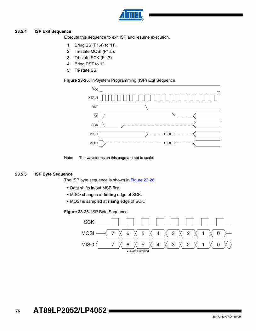
23.5.4 ISP Exit Sequence Execute this sequence to exit ISP and resume execution.
1. Bring SS (P1.4) to “H”.
2. Tri-state MOSI (P1.5).
3. Tri-state SCK (P1.7).
4. Bring RST to “L”.
5. Tri-state SS.
Figure 23-25. In-System Programming (ISP) Exit Sequence
Note: The waveforms on this page are not to scale.
23.5.5 ISP Byte SequenceThe ISP byte sequence is shown in Figure 23-26.
• Data shifts in/out MSB first.
• MISO changes at falling edge of SCK.
• MOSI is sampled at rising edge of SCK.
Figure 23-26. ISP Byte Sequence
VCC
RST
SS
SCK
HIGH Z
MOSI HIGH Z
MISO
XTAL1
7
7
6
6
5
5
4
4
3
3
2
2
1
1
0
0
MOSI
MISO
SCK
Data Sampled
763547J–MICRO–10/09
AT89LP2052/LP4052
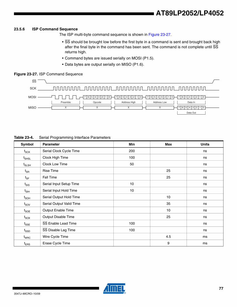
AT89LP2052/LP4052
23.5.6 ISP Command Sequence The ISP multi-byte command sequence is shown in Figure 23-27.
• SS should be brought low before the first byte in a command is sent and brought back high after the final byte in the command has been sent. The command is not complete until SS returns high.
• Command bytes are issued serially on MOSI (P1.5).
• Data bytes are output serially on MISO (P1.6).
Figure 23-27. ISP Command Sequence
7 06 5 4 3 2 1 7 06 5 4 3 2 1 7 06 5 4 3 2 1 7 06 5 4 3 2 1
7 06 5 4 3 2 1
SS
SCK
MOSI
MISO
Preamble Opcode Address High Address Low Data In
Data Out
X X X X
Table 23-4. Serial Programming Interface Parameters
Symbol Parameter Min Max Units
tSCK Serial Clock Cycle Time 200 ns
tSHSL Clock High Time 100 ns
tSLSH Clock Low Time 50 ns
tSR Rise Time 25 ns
tSF Fall Time 25 ns
tSIS Serial Input Setup Time 10 ns
tSIH Serial Input Hold Time 10 ns
tSOH Serial Output Hold Time 10 ns
tSOV Serial Output Valid Time 35 ns
tSOE Output Enable Time 10 ns
tSOX Output Disable Time 25 ns
tSSE SS Enable Lead Time 100 ns
tSSD SS Disable Lag Time 100 ns
tWRC Wire Cycle Time 4.5 ms
tERS Erase Cycle Time 9 ms
773547J–MICRO–10/09
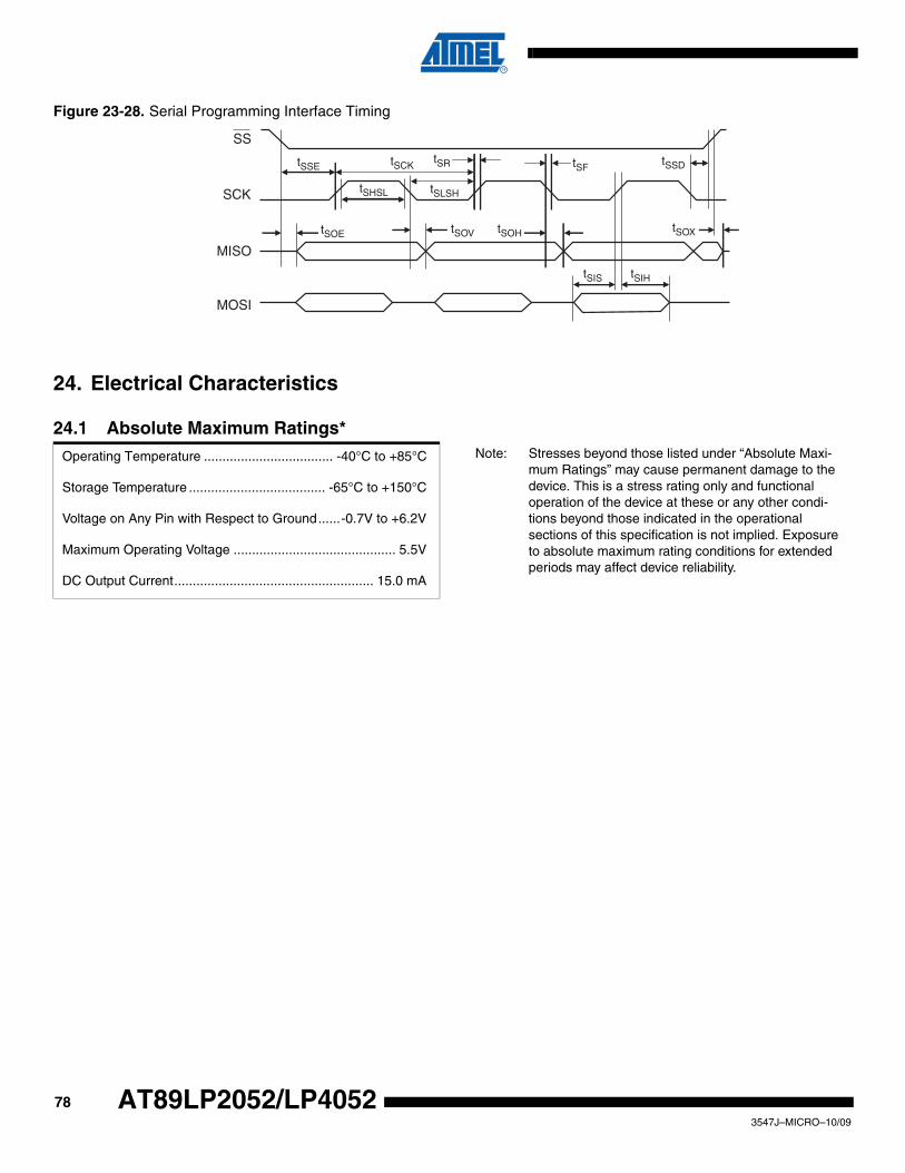
Figure 23-28. Serial Programming Interface Timing
tSRtSSE
tSLSH
tSOV
tSF
tSOX
tSSDtSCK
tSHSL
tSOE tSOH
tSIHtSIS
SS
SCK
MISO
MOSI
24. Electrical Characteristics
24.1 Absolute Maximum Ratings*
Operating Temperature ................................... -40°C to +85°C Note: Stresses beyond those listed under “Absolute Maxi-mum Ratings” may cause permanent damage to the device. This is a stress rating only and functional operation of the device at these or any other condi-tions beyond those indicated in the operational sections of this specification is not implied. Exposure to absolute maximum rating conditions for extended periods may affect device reliability.
Storage Temperature ..................................... -65°C to +150°C
Voltage on Any Pin with Respect to Ground......-0.7V to +6.2V
Maximum Operating Voltage ............................................ 5.5V
DC Output Current...................................................... 15.0 mA
783547J–MICRO–10/09
AT89LP2052/LP4052
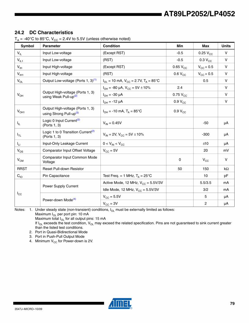
AT89LP2052/LP4052
Notes: 1. Under steady state (non-transient) conditions, IOL must be externally limited as follows:Maximum IOL per port pin: 10 mAMaximum total IOL for all output pins: 15 mAIf IOL exceeds the test condition, VOL may exceed the related specification. Pins are not guaranteed to sink current greater than the listed test conditions.
2. Port in Quasi-Bidirectional Mode3. Port in Push-Pull Output Mode4. Minimum VCC for Power-down is 2V.
24.2 DC CharacteristicsTA = -40°C to 85°C, VCC = 2.4V to 5.5V (unless otherwise noted)
Symbol Parameter Condition Min Max Units
VIL Input Low-voltage (Except RST) -0.5 0.25 VCC V
VIL1 Input Low-voltage (RST) -0.5 0.3 VCC V
VIH Input High-voltage (Except RST) 0.65 VCC VCC + 0.5 V
VIH1 Input High-voltage (RST) 0.6 VCC VCC + 0.5 V
VOL Output Low-voltage (Ports 1, 3)(1) IOL = 10 mA, VCC = 2.7V, TA = 85°C 0.5 V
VOHOutput High-voltage (Ports 1, 3) using Weak Pull-up(2)
IOH = -80 µA, VCC = 5V ± 10% 2.4 V
IOH = -30 µA 0.75 VCC V
IOH = -12 µA 0.9 VCC V
VOH1Output High-voltage (Ports 1, 3)
using Strong Pull-up(3) IOH = -10 mA, TA = 85°C 0.9 VCC
IILLogic 0 Input Current(2)
(Ports 1, 3)VIN = 0.45V -50 µA
ITLLogic 1 to 0 Transition Current(2) (Ports 1, 3)
VIN = 2V, VCC = 5V ± 10% -300 µA
ILI Input-Only Leakage Current 0 < VIN < VCC ±10 µA
VOS Comparator Input Offset Voltage VCC = 5V 20 mV
VCMComparator Input Common Mode Voltage
0 VCC V
RRST Reset Pull-down Resistor 50 150 kΩ
CIO Pin Capacitance Test Freq. = 1 MHz, TA = 25°C 10 pF
ICC
Power Supply CurrentActive Mode, 12 MHz, VCC = 5.5V/3V 5.5/3.5 mA
Idle Mode, 12 MHz, VCC = 5.5V/3V 3/2 mA
Power-down Mode(4)VCC = 5.5V 5 µA
VCC = 3V 2 µA
793547J–MICRO–10/09
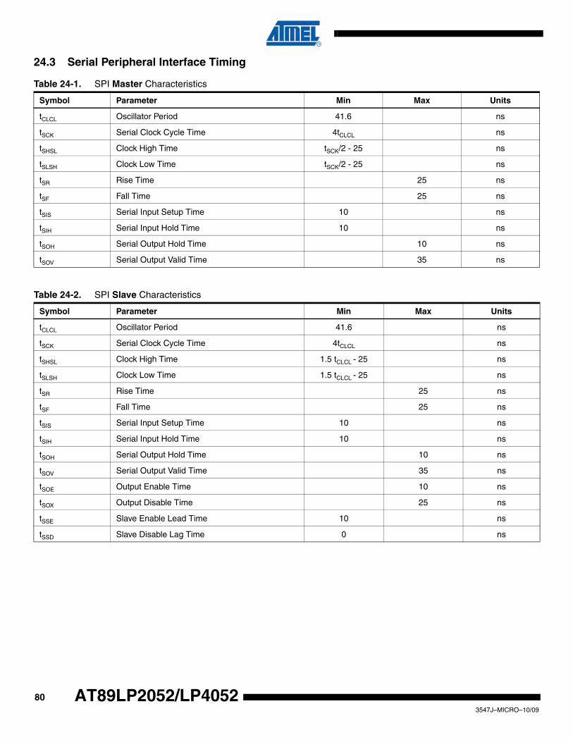
24.3 Serial Peripheral Interface Timing
Table 24-1. SPI Master Characteristics
Symbol Parameter Min Max Units
tCLCL Oscillator Period 41.6 ns
tSCK Serial Clock Cycle Time 4tCLCL ns
tSHSL Clock High Time tSCK/2 - 25 ns
tSLSH Clock Low Time tSCK/2 - 25 ns
tSR Rise Time 25 ns
tSF Fall Time 25 ns
tSIS Serial Input Setup Time 10 ns
tSIH Serial Input Hold Time 10 ns
tSOH Serial Output Hold Time 10 ns
tSOV Serial Output Valid Time 35 ns
Table 24-2. SPI Slave Characteristics
Symbol Parameter Min Max Units
tCLCL Oscillator Period 41.6 ns
tSCK Serial Clock Cycle Time 4tCLCL ns
tSHSL Clock High Time 1.5 tCLCL - 25 ns
tSLSH Clock Low Time 1.5 tCLCL - 25 ns
tSR Rise Time 25 ns
tSF Fall Time 25 ns
tSIS Serial Input Setup Time 10 ns
tSIH Serial Input Hold Time 10 ns
tSOH Serial Output Hold Time 10 ns
tSOV Serial Output Valid Time 35 ns
tSOE Output Enable Time 10 ns
tSOX Output Disable Time 25 ns
tSSE Slave Enable Lead Time 10 ns
tSSD Slave Disable Lag Time 0 ns
803547J–MICRO–10/09
AT89LP2052/LP4052
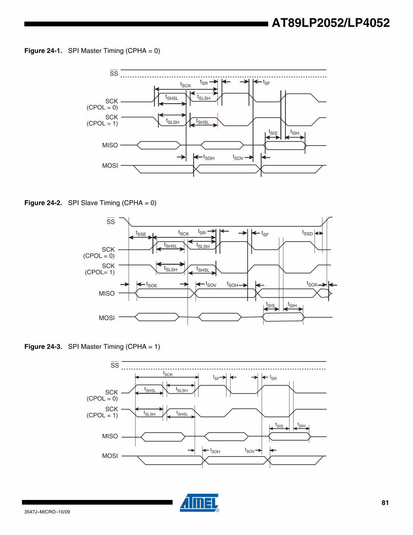
AT89LP2052/LP4052
Figure 24-1. SPI Master Timing (CPHA = 0)
Figure 24-2. SPI Slave Timing (CPHA = 0)
Figure 24-3. SPI Master Timing (CPHA = 1)
SS
SCK(CPOL = 0)
SCK(CPOL = 1)
MISO
MOSI
tSRtSCK
tSLSH
tSLSH
tSHSL
tSHSL
tSOH
tSF
tSIS tSIH
tSOV
tSRtSSE
tSLSH
tSHSL
tSOV
tSF
tSOX
tSSDtSCK
tSLSH
tSHSL
tSOE tSOH
tSIHtSIS
SS
SCK(CPOL = 0)
SCK(CPOL= 1)
MISO
MOSI
tSHSL tSLSH
tSHSLtSLSH
tSCK
tSOH
tSF tSR
tSIS
tSOV
tSIH
SS
SCK(CPOL = 0)
SCK(CPOL = 1)
MISO
MOSI
813547J–MICRO–10/09
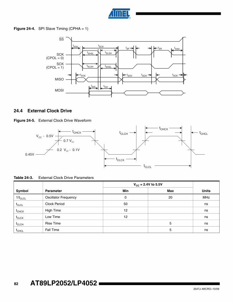
Figure 24-4. SPI Slave Timing (CPHA = 1)
24.4 External Clock Drive
Figure 24-5. External Clock Drive Waveform
SS
SCK(CPOL = 0)
SCK(CPOL = 1)
MISO
MOSI
tSCKtSSE
tSHSL
tSHSLtSLSH
tSLSH
tSSD
tSIHtSIS
tSOE tSOV tSOH tSOX
tSF tSR
Table 24-3. External Clock Drive Parameters
Symbol Parameter
VCC = 2.4V to 5.5V
UnitsMin Max
1/tCLCL Oscillator Frequency 0 20 MHz
tCLCL Clock Period 50 ns
tCHCX High Time 12 ns
tCLCX Low Time 12 ns
tCLCH Rise Time 5 ns
tCHCL Fall Time 5 ns
823547J–MICRO–10/09
AT89LP2052/LP4052
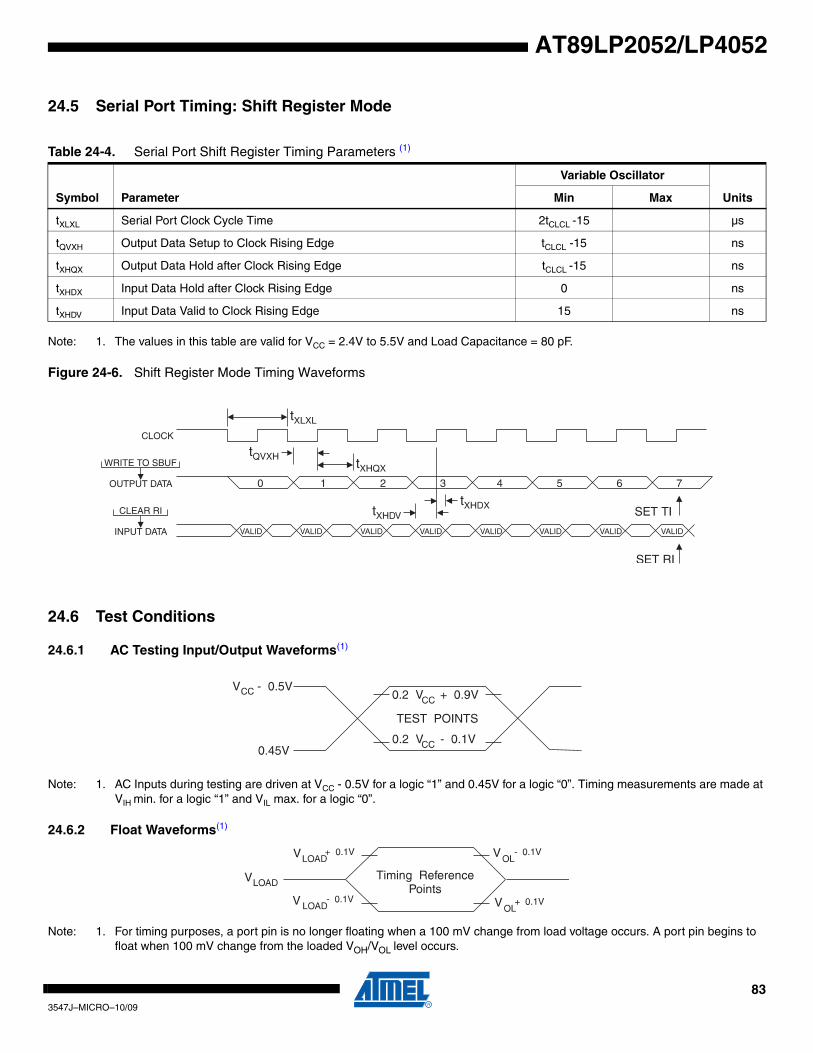
AT89LP2052/LP4052
Note: 1. The values in this table are valid for VCC = 2.4V to 5.5V and Load Capacitance = 80 pF.
Figure 24-6. Shift Register Mode Timing Waveforms
24.6 Test Conditions
24.6.1 AC Testing Input/Output Waveforms(1)
Note: 1. AC Inputs during testing are driven at VCC - 0.5V for a logic “1” and 0.45V for a logic “0”. Timing measurements are made at VIH min. for a logic “1” and VIL max. for a logic “0”.
24.6.2 Float Waveforms(1)
Note: 1. For timing purposes, a port pin is no longer floating when a 100 mV change from load voltage occurs. A port pin begins to float when 100 mV change from the loaded VOH/VOL level occurs.
24.5 Serial Port Timing: Shift Register Mode
Table 24-4. Serial Port Shift Register Timing Parameters (1)
Symbol Parameter
Variable Oscillator
UnitsMin Max
tXLXL Serial Port Clock Cycle Time 2tCLCL -15 µs
tQVXH Output Data Setup to Clock Rising Edge tCLCL -15 ns
tXHQX Output Data Hold after Clock Rising Edge tCLCL -15 ns
tXHDX Input Data Hold after Clock Rising Edge 0 ns
tXHDV Input Data Valid to Clock Rising Edge 15 ns
0 1 2 3 4 5 6 7
VALID VALID VALID VALID VALID VALID VALID VALID
CLOCK
WRITE TO SBUF
OUTPUT DATA
CLEAR RI
INPUT DATA
833547J–MICRO–10/09
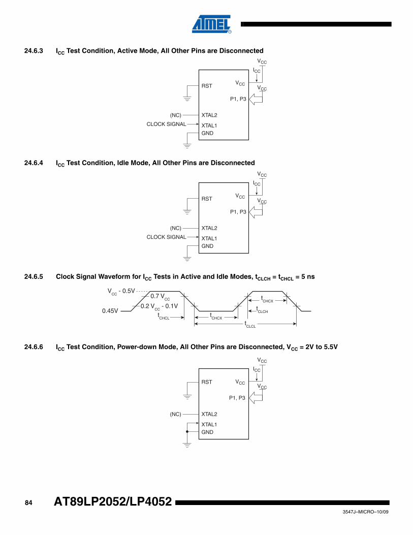
24.6.3 ICC Test Condition, Active Mode, All Other Pins are Disconnected
24.6.4 ICC Test Condition, Idle Mode, All Other Pins are Disconnected
24.6.5 Clock Signal Waveform for ICC Tests in Active and Idle Modes, tCLCH = tCHCL = 5 ns
24.6.6 ICC Test Condition, Power-down Mode, All Other Pins are Disconnected, VCC = 2V to 5.5V
XTAL2
RSTVCC
VCC
VCC
ICC
XTAL1
P1, P3
GND
(NC)
CLOCK SIGNAL
XTAL2
RSTVCC
VCC
VCC
ICC
XTAL1
P1, P3
GND
(NC)
CLOCK SIGNAL
VCC
- 0.5V
0.45V0.2 V
CC - 0.1V
0.7 VCC
tCHCX
tCHCX
tCLCH
tCHCL
tCLCL
XTAL2
RST VCC
VCC
VCC
ICC
XTAL1
P1, P3
GND
(NC)
843547J–MICRO–10/09
AT89LP2052/LP4052
AT89LP2052/LP4052
25. Ordering Information
25.1 Green Package Option (Pb/Halide-free)Speed(MHz)
PowerSupply Ordering Code Package Operation Range
20 2.4V to 5.5V
AT89LP2052-20PU
AT89LP2052-20SUAT89LP2052-20XU
20P320S220X Industrial
(-40⋅ C to 85⋅ C)AT89LP4052-20PU
AT89LP4052-20SUAT89LP4052-20XU
20P3
20S220X
Package Type
20P3 20-lead, 0.300” Wide, Plastic Dual In-line Package (PDIP)
20S2 20-lead, 0.300” Wide, Plastic Gull Wing Small Outline (SOIC)
20X 20-lead, 4.4 mm Body Width, Plastic Thin Shrink Small Outline Package (TSSOP)
853547J–MICRO–10/09
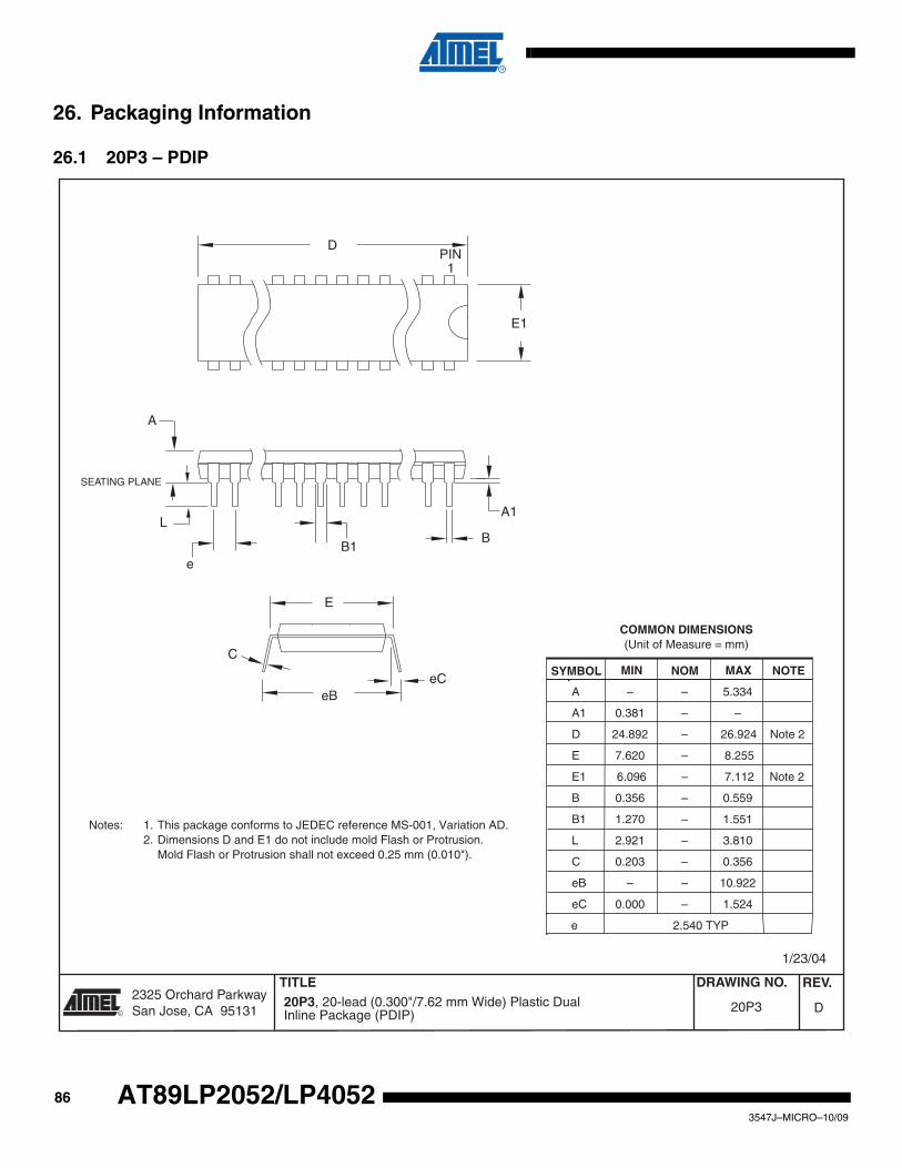
26. Packaging Information
26.1 20P3 – PDIP
2325 Orchard Parkway San Jose, CA 95131
TITLE DRAWING NO.
R
REV. 20P3, 20-lead (0.300"/7.62 mm Wide) Plastic Dual Inline Package (PDIP) D20P3
1/23/04
PIN1
E1
A1
B
E
B1
C
L
SEATING PLANE
A
D
e
eBeC
COMMON DIMENSIONS(Unit of Measure = mm)
SYMBOL MIN NOM MAX NOTE
A – – 5.334
A1 0.381 – –
D 24.892 – 26.924 Note 2
E 7.620 – 8.255
E1 6.096 – 7.112 Note 2
B 0.356 – 0.559
B1 1.270 – 1.551
L 2.921 – 3.810
C 0.203 – 0.356
eB – – 10.922
eC 0.000 – 1.524
e 2.540 TYP
Notes: 1. This package conforms to JEDEC reference MS-001, Variation AD. 2. Dimensions D and E1 do not include mold Flash or Protrusion.
Mold Flash or Protrusion shall not exceed 0.25 mm (0.010").
863547J–MICRO–10/09
AT89LP2052/LP4052
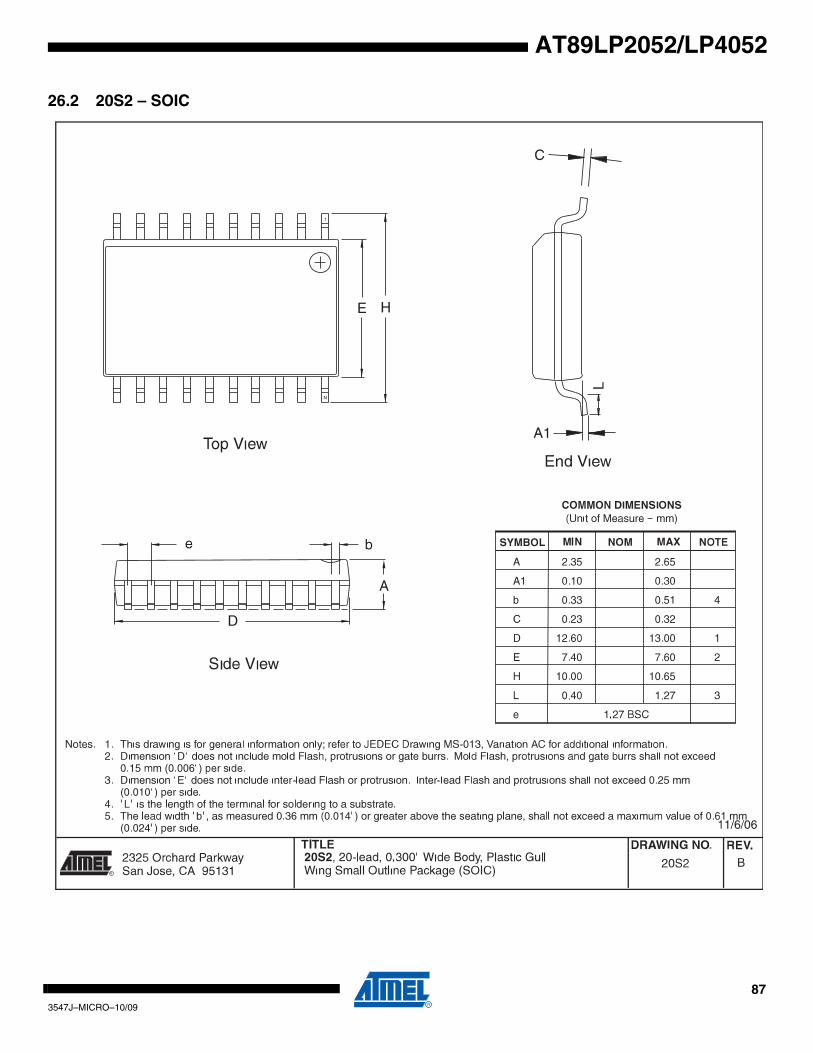
AT89LP2052/LP4052
26.2 20S2 – SOIC
873547J–MICRO–10/09
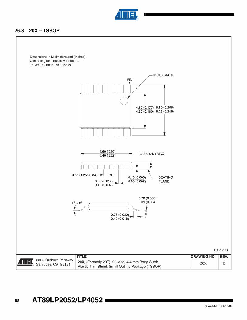
26.3 20X – TSSOP
2325 Orchard Parkway San Jose, CA 95131
TITLE DRAWING NO.
R
REV. 20X, (Formerly 20T), 20-lead, 4.4 mm Body Width, Plastic Thin Shrink Small Outline Package (TSSOP)
C20X
10/23/03
6.60 (.260)6.40 (.252) 1.20 (0.047) MAX
0.65 (.0256) BSC
0.20 (0.008)0.09 (0.004)
0.15 (0.006)0.05 (0.002)
INDEX MARK
6.50 (0.256)6.25 (0.246)
SEATINGPLANE
4.50 (0.177)4.30 (0.169)
PIN1
0.75 (0.030)0.45 (0.018)
0º ~ 8º
0.30 (0.012)0.19 (0.007)
Dimensions in Millimeters and (Inches). Controlling dimension: Millimeters.JEDEC Standard MO-153 AC
883547J–MICRO–10/09
AT89LP2052/LP4052
AT89LP2052/LP4052
27. Revision History
Revision A – March 2005 • Initial Release
Revision B – June 2005 • Last paragraph in Section 13.2 on page 15 was inserted.
Revision C – August 2005
• In Table 16-3 on page 26, changed the SFR address for TCONB from 88H to 91H.
• Changed the Maximum Bit Frequency from f/2 to f/4 in the “Serial Peripheral Interface” on page 42.
• In the “SPI Block Diagram” on page 43, the 16-bit reference was deleted from Shift Register box.
• In the “SPSR – SPI Status Register” on page 46, the Divider ratios were changed to the following: ÷4÷8÷32÷64
• Replaced CM3 with CM2 in Bit 2 of register ACSR (page 50)
• In the “Programming Command Summary” on page 58, several changes were made in specific bit positions within the Addr High, Addr Low and Data 0 columns.
Revision D – April 2006 • Added ROHS compliant device offerings.
Revision E – June 2006• In pages 1, 82 and 83, the reference to VCC = 2.7V were changed to 2.4V. On page 79 the
maximum rating for the operating temperature was changed from +125⋅ C to +85⋅ C.
Revision F – June 2006 • In Table 6-1 on page 6, changed the SFR address of SPDR from 85H to 86H.
Revision G – April 2007• In section 7.8 ”Reset” on page 8 changed the polarity of the RST input signal requirement
from low to high.
• Added Section 11. “Oscillator Characteristics” on page 11.
Revision H – May 2007• Changed TMOD to TCON (Table 16-1 on page 27).
• Changed SPI = 1 and SPI = 0 to SPE = 1 and SPE = 0 (Table 19-1 on page 45).
Revision I – June 2008 • Removed Standard Packaging Offering.
Revision J – Oct. 2009• Added R1 option to oscillator connection diagram Figure 11-1 on page 11.
• Added related oscillator amplitude graphs Figures 11-3 and 11-5.
893547J–MICRO–10/09

903547J–MICRO–10/09
AT89LP2052/LP4052
AT89LP2052/LP4052
Table of Contents
1. Description ............................................................................................... 1
2. Pin Configuration ..................................................................................... 2
2.1 20-lead PDIP/SOIC/TSSOP ..................................................................................2
3. Pin Description ......................................................................................... 3
4. Block Diagram .......................................................................................... 4
5. Memory Organization .............................................................................. 4
5.1 Program Memory ...................................................................................................4
5.2 Data Memory .........................................................................................................5
6. Special Function Registers ..................................................................... 6
7. Comparison to Standard 8051 ................................................................ 7
7.1 System Clock ........................................................................................................7
7.2 Instruction Execution with Single-cycle Fetch .......................................................7
7.3 Interrupt Handling ..................................................................................................7
7.4 Timer/Counters ......................................................................................................7
7.5 Serial Port ..............................................................................................................7
7.6 Watchdog Timer ....................................................................................................7
7.7 I/O Ports ................................................................................................................8
7.8 Reset .....................................................................................................................8
8. Enhanced CPU ......................................................................................... 8
9. Restrictions on Certain Instructions .................................................... 10
9.1 Branching Instructions .........................................................................................10
9.2 MOVX-related Instructions, Data Memory ...........................................................10
10. System Clock ......................................................................................... 10
10.1 Crystal Oscillator .................................................................................................10
10.2 External Clock Source .........................................................................................10
10.3 System Clock Out ................................................................................................10
11. Oscillator Characteristics ..................................................................... 11
12. Reset ....................................................................................................... 14
12.1 Power-on Reset ...................................................................................................14
12.2 Brown-out Reset ..................................................................................................14
i3547J–MICRO–10/09
Table of Contents (Continued)12.3 External Reset .....................................................................................................14
12.4 Watchdog Reset ..................................................................................................14
13. Power Saving Modes ............................................................................. 14
13.1 Idle Mode .............................................................................................................15
13.2 Power-down Mode ..............................................................................................15
14. Interrupts ................................................................................................ 16
14.1 Interrupt Response Time .....................................................................................17
15. I/O Ports .................................................................................................. 20
15.1 Quasi-bidirectional Output ...................................................................................20
15.2 Input-only Mode ...................................................................................................21
15.3 Open-drain Output ...............................................................................................22
15.4 Push-pull Output ..................................................................................................22
15.5 Port 1 Analog Functions ......................................................................................22
15.6 Port Read-Modify-Write .......................................................................................23
15.7 Port Alternate Functions ......................................................................................23
16. Enhanced Timer/Counters .................................................................... 24
16.1 Mode 0 ................................................................................................................24
16.2 Mode 1 ................................................................................................................25
16.3 Mode 2 ................................................................................................................26
16.4 Mode 3 ................................................................................................................26
16.5 Pulse Width Modulation .......................................................................................29
16.6 Timer/Counter Pin Configuration .........................................................................30
17. External Interrupts ................................................................................. 30
18. Serial Interface ....................................................................................... 31
18.1 Multiprocessor Communications .........................................................................31
18.2 Baud Rates ..........................................................................................................33
18.3 More About Mode 0 .............................................................................................34
18.4 More About Mode 1 .............................................................................................36
18.5 More About Modes 2 and 3 .................................................................................38
18.6 Framing Error Detection ......................................................................................41
18.7 Automatic Address Recognition ..........................................................................41
ii3547J–MICRO–10/09
AT89LP2052/LP4052
AT89LP2052/LP4052
Table of Contents (Continued)
19. Serial Peripheral Interface ..................................................................... 42
19.1 Normal Mode .......................................................................................................44
19.2 Enhanced Mode ..................................................................................................44
19.3 Serial Clock Generator ........................................................................................47
19.4 SPI Pin Configuration ..........................................................................................48
20. Analog Comparator ............................................................................... 49
20.1 Comparator Interrupt with Debouncing ...............................................................49
21. Programmable Watchdog Timer ........................................................... 51
22. Instruction Set Summary ...................................................................... 52
23. Programming the Flash Memory .......................................................... 57
23.1 Programming Command Summary .....................................................................58
23.2 Status Register ....................................................................................................59
23.3 DATA Polling .......................................................................................................59
23.4 Parallel Programming ..........................................................................................59
23.5 In-System Programming (ISP) ............................................................................73
24. Electrical Characteristics ...................................................................... 78
24.1 Absolute Maximum Ratings* ...............................................................................78
24.2 DC Characteristics ..............................................................................................79
24.3 Serial Peripheral Interface Timing ......................................................................80
24.4 External Clock Drive ............................................................................................82
24.5 Serial Port Timing: Shift Register Mode ..............................................................83
24.6 Test Conditions ...................................................................................................83
25. Ordering Information ............................................................................. 85
25.1 Green Package Option (Pb/Halide-free) .............................................................85
26. Packaging Information .......................................................................... 86
26.1 20P3 – PDIP ........................................................................................................86
26.2 20S2 – SOIC ......................................................................................................87
26.3 20X – TSSOP ......................................................................................................88
27. Revision History ..................................................................................... 89
iii3547J–MICRO–10/09
3547J–MICRO–10/09
Headquarters International
Atmel Corporation2325 Orchard ParkwaySan Jose, CA 95131USATel: 1(408) 441-0311Fax: 1(408) 487-2600
Atmel AsiaRoom 1219Chinachem Golden Plaza77 Mody Road TsimshatsuiEast KowloonHong KongTel: (852) 2721-9778Fax: (852) 2722-1369
Atmel EuropeLe Krebs8, Rue Jean-Pierre TimbaudBP 30978054 Saint-Quentin-en-Yvelines CedexFranceTel: (33) 1-30-60-70-00 Fax: (33) 1-30-60-71-11
Atmel Japan9F, Tonetsu Shinkawa Bldg.1-24-8 ShinkawaChuo-ku, Tokyo 104-0033JapanTel: (81) 3-3523-3551Fax: (81) 3-3523-7581
Product Contact
Web Sitewww.atmel.com
Technical [email protected]
Sales Contactwww.atmel.com/contacts
Literature Requestswww.atmel.com/literature
Disclaimer: The information in this document is provided in connection with Atmel products. No license, express or implied, by estoppel or otherwise, to anyintellectual property right is granted by this document or in connection with the sale of Atmel products. EXCEPT AS SET FORTH IN ATMEL’S TERMS AND CONDI-TIONS OF SALE LOCATED ON ATMEL’S WEB SITE, ATMEL ASSUMES NO LIABILITY WHATSOEVER AND DISCLAIMS ANY EXPRESS, IMPLIED OR STATUTORYWARRANTY RELATING TO ITS PRODUCTS INCLUDING, BUT NOT LIMITED TO, THE IMPLIED WARRANTY OF MERCHANTABILITY, FITNESS FOR A PARTICULARPURPOSE, OR NON-INFRINGEMENT. IN NO EVENT SHALL ATMEL BE LIABLE FOR ANY DIRECT, INDIRECT, CONSEQUENTIAL, PUNITIVE, SPECIAL OR INCIDEN-TAL DAMAGES (INCLUDING, WITHOUT LIMITATION, DAMAGES FOR LOSS OF PROFITS, BUSINESS INTERRUPTION, OR LOSS OF INFORMATION) ARISING OUT OFTHE USE OR INABILITY TO USE THIS DOCUMENT, EVEN IF ATMEL HAS BEEN ADVISED OF THE POSSIBILITY OF SUCH DAMAGES. Atmel makes norepresentations or warranties with respect to the accuracy or completeness of the contents of this document and reserves the right to make changes to specificationsand product descriptions at any time without notice. Atmel does not make any commitment to update the information contained herein. Unless specifically providedotherwise, Atmel products are not suitable for, and shall not be used in, automotive applications. Atmel’s products are not intended, authorized, or warranted for useas components in applications intended to support or sustain life.
© 2009 Atmel Corporation. All rights reserved. Atmel®, logo and combinations thereof, and others are registered trademarks or trademarks ofAtmel Corporation or its subsidiaries. Other terms and product names may be trademarks of others.