Cam seminar
24
VISVESVARAYA NATIONAL INSTITUTE OF TECHNOLOGY NAGPUR DEPARTMENT OF MECHANICAL ENGINEERING SEMINAR ON “ ” GUIDED BY: PROF. Y. M. PURI CAD/CAD ENGG. PREPARED BY: BHUPESH D. SARODE CAD/CAM ENGG. FIRST SEM 2012-13
-
Upload
akash-maurya -
Category
Engineering
-
view
96 -
download
0
Transcript of Cam seminar

VISVESVARAYA NATIONAL INSTITUTE OF TECHNOLOGY NAGPUR
DEPARTMENT OF MECHANICAL ENGINEERING
SEMINAR ON
“ ”
GUIDED BY:PROF. Y. M. PURICAD/CAD ENGG.
PREPARED BY: BHUPESH D. SARODE CAD/CAM ENGG.FIRST SEM
2012-13

Scope Of Presentation What is MicromachiningTypes of Machines in MicromachiningVarious Micro Machines
Etching Process, Bulk Micromachining,Surface Micromachining,LIGA ProcessEDM
Application

MICRO-MACHINING
• Micromachining is the basic technology for fabrication of micro-components of size in the range of 1 to 500 micrometers
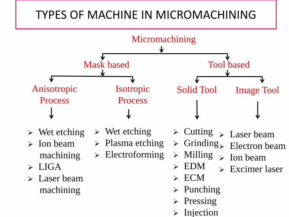
TYPES OF MACHINE IN MICROMACHINING
Tool based
Solid Tool Image ToolIsotropic
Process
Micromachining
Mask based
Anisotropic
Process
Wet etching
Ion beam
machining
LIGA
Laser beam
machining
Laser beam
Electron beam
Ion beam
Excimer laser
Wet etching
Plasma etching
Electroforming
Cutting
Grinding
Milling
EDM
ECM
Punching
Pressing
Injection

Micro-Machining Processes
5
Micro-Machining
ETCHINGBulk
Micro-
Machining
Surface
Micro-
Machining
LIGA EDM

ETCHING PROCESS
Etching process consists of three steps:
Mass transport of reactants (through a boundary layer)
to the surface to be etched
Reaction between reactants and the film(s) to be
etched at the surface
Mass transport of reaction products from the surface
through the boundary layer

ETCHING PROCESS
• Isotropic vs. Anisotropic
• Isotropic– etch rate is same in all directions
• Anisotropic– etch rate is orientation dependent
• Dry vs. Wet
• Dry– uses gas-phase process
• Wet– uses liquid-phase process

WET ETCHING PROCESS DESCRIPTION
The wet etching process involves :
Performed in an immersion tank
Wafers in wafer carrier are lowered into etchant solution
Wafers remain in solution for specified amount of time
.referred to as etch duration
Wafer carrier is removed from solution
Wafers are rinsed in deionized water
Wafers are dried

BULK MICROMACHINING
• Process for producing 3D MEMS structures –older process
• Uses anisotropic etching of single crystal silicon
Example: silicon cantilever beam for atomic force microscope

Dopant Diffusion
Masking
Anisotropic Etching
BULK MICROMACHINING

• Newer process for producing MEMS structures
• Uses etching techniques to pattern micro-scale structures from polycrystalline (poly) silicon, or metal alloys
• Examples: accelerometers, pressure sensors, micro gears and transmissions,micro mirrors etc.
SURFACE MICROMACHINING

SURFACE MICROMACHINING
(a) DEPOSITION OF
POLYSILICON;
(b) ETCHING OF
POLYSILICON;
(c) SELECTIVE WET
ETCHING OF PSG,
LEAVING THE
SILICON
SUBSTRATE AND
DEPOSITED
POLYSILICON
UNAFFECTED

GERMANACRONYM
LITHOGRAPHIE -----------------LITHOGRAPHY
GALVANOFORMUNG -------------- ELECTROFORMING
ABFORMNG -----------------------------MOLDING
LIGA

LIGA
X-ray Irradiation
Resist Development
Electroforming
Resist Removal

VIDEO ON LIGA

workpiece+anode
-cathode
(a) Tool and workpiece immersed in
dielectric liquid.
(b) A spark is generated between tool and
workpiece.
(c) The high temperature causes the melting
and vaporization of electrodes.
(d) At the end of the pulse, the molten
material is ejected from surface, leaving a
shallow crater.
electrode
Material Removal Mechanism of EDM

Micro EDM Equipment

VIDEO ON EDM

1. Machine any conductive materials.
2. Single or medium size production.
3. Slots and Arbitrary 3D micro molds.
Capabilities of Micro EDM

MICRO-LATHE


MICRO-FACTORY
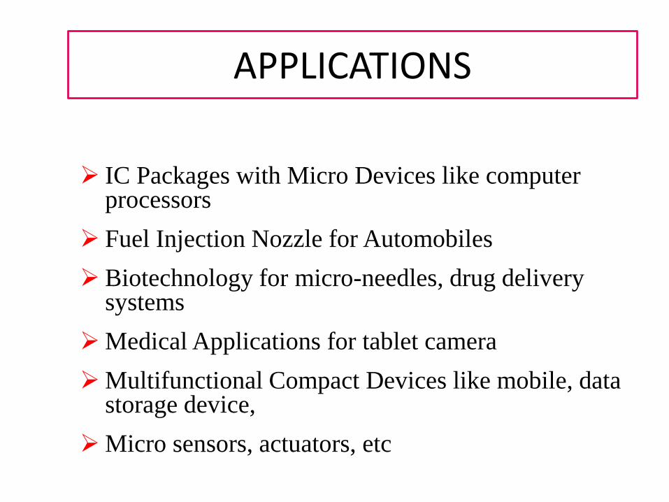
APPLICATIONS
IC Packages with Micro Devices like computer processors
Fuel Injection Nozzle for Automobiles
Biotechnology for micro-needles, drug delivery systems
Medical Applications for tablet camera
Multifunctional Compact Devices like mobile, data storage device,
Micro sensors, actuators, etc

THANK YOU