C~474 < 1DTIC - Defense Technical Information Center i. basic discrete cosine transform theory ......
138
NAVAL POSTGRADUATE SCHOOIL Monterey, California 00= C~474 < 1DTIC G A .. E EC T E 1 SE 04199U. THESIS VHDL BEHAVIORAL DESCRIPTION OF DISCRETE COSINE TRANSFORM IN IMAGE COMPRESSION by DENG, AN-TE September 1991 Thesis Advisor: Chin-Hwa Lee Approved for public release; distribution is unlimited 92-02637 /I/IlII llii ll~/ll 'Ii l
Transcript of C~474 < 1DTIC - Defense Technical Information Center i. basic discrete cosine transform theory ......

NAVAL POSTGRADUATE SCHOOILMonterey, California
00=
C~474
< 1DTICG A ..E EC T E 1
SE 04199U.
THESISVHDL BEHAVIORAL DESCRIPTIONOF DISCRETE COSINE TRANSFORM
IN IMAGE COMPRESSION
by
DENG, AN-TE
September 1991Thesis Advisor: Chin-Hwa Lee
Approved for public release; distribution is unlimited
92-02637/I/IlII llii ll~/ll 'Ii l

L: nclassifiedSECURITY CLASSIFICATION OF THIS PAGE
REPORT DOCUMENTATION PAGEla REPORT SECURITY CLASSIFICATION I b RESTRICTIVE MARKINGSiUclassified
2a SECURITY CLASSIFICATION AUTHORITY 3 DISTRIBUTIONiAVAILABILiTY OF REPORT
Appruvcd for public riieose, distribution is uniiiiited2b DECLASSFICATIONDOVVNGRADING SCHEDULE
4 PERFORMiNGORCPANiZATION REPORT NuMBER(S) 5 MONITORING C' 2GANIZATiOr REPORT NUMBER(S)
6a NAME OF PERFORMING ORGANIZATION 6b OIiCE SYMBOL 7a NAME OF MONITORING ORGANiZATIGNNai dl P'ostgraduate School J (it applicable) Na'. a[ Postgradluate Sclii,,
6c ADDRESS (City, State, and ZIP Code) 7b ADDRESS (City, State, and ZIP Code)Monterey, CA 93943-5U Monterey, CA 93943-50U00
Ba NAME OF FUNDINGSPONSORING Bb OFFICE SYMBOL 9 PROCUREMENT INSTRUMENT iDENTIFfCATiON NUMBERORGANIZATION (it applicable)
Br ADDRE SS (City, State, and ZIP Code) 10 SOURCE OF FUNDING NUMBERS
11 1 TLE (include Security Classification)
VllIll. fie ha% uralI Description of*Discrete Cumiiic lTraiisform in Digital Image Cumipression
12 PERSONAL AUTHOR(S) Deng. An-Te
13a TYPE OF REPORT 13b TIME COVERED 14DTORPORT (year, monhdy 15AGCiTM1aster's Thesis From To Sep .ember 19sl 139
16 SUPPLEMENTARY NOTATIONThe views expressed in this thesis are those ot the author and do not reflect the official policy or position ot the D~epartment iffDefense or thu L SIni'.e rn ment.17 COSATI CODES 18 SUBJECT TERMS (continue on reverse if necessary and identify by block number)
FIELD GROUP SUBGROUP Image Compression, Discrete Cosine Transform; VHFSIC I lard~v re D~escription Language.*Top Down design;
19 ABSTRACT (continue on reverse it necessary and identify by block number)
T[his thesis describes a VHSIC Hardware Description Language i VHDU simulation ul d hardware 8 x 6 D)iscrete Cosine Translorin i DCTi W hichcan be applied to image compreasin. A Top-Down Design approach is taken in the study, a discussion (it D('T theiiry is presented, along with adescription of the I -D DCT circuit architecture and its simuliation in VHDL. Results of the 2-D DCT simulation are included for two simple testpatterns and verified by hand calculation, demonstrating the validity of the simulation. Shortcomingb bound in the simulation are described,together with suggestions for correcting them. In the future, the VHDL description of the 8 z 8 image block 2 1) [)cr Lan be further developed inuostructural and gate-level description, after which hardware circwut implementation can occur.
20 DISTRIBUTION/AVAILABILITY OF ABSTRACT 21 ABSTRACT SECURITY CLASSIFICATION
EluNCi ASS41iD UNLIMITED 1 SAIt Asi.PT Htric 3 UsTISIES Unclassified
22a NAME OF RESPONSIBLE INDIVIDUAL 22b TELEPHONE (include Area code) f22c OFFICE SYMBOLChin-Fi1wa L.ee 14081 646-2190 IECDD FORM 1473,84 MAR 83 APR edition may be used until exhausted SECURITY CLASSIFICATION OF THIS PAGE
All other editions are obsolete Unclassified

Approved for public release; distribut , is unlimited.
VHDL Behavioral Descriptionof Discrete Cosine Transform
in Image Compression
by
DENG, AN-TELt. Col, Republic of China Army
B.S., Chung Cheng Institute of Technology, 1976
Submitted in partial fulfillmentof the requirements for the degree of
MASTER OF SCIENCE IN SYSTEM ENGINEERING
from the
NAVAL POSTGRADUATE SCHOOL
September 1991
Author: _ _ _ _ _ _ _ _ __,
IQENj AN-TE
Approved by:n-Hwa e esis Advisor (
oberto Cristi,-ond Reader
JiephStrnberg, Charan
Department of Electronic Warfare
ii

ABSTRACT
This thesis describes a VHSIC Hardware Description Language (VHDL) simulation of
a hardware 8 x 8 Discrete Cosine Transform (DCT) which can be applied to image
compression. A Top-Down Design approach is taken in the study, a discussion of DCT theory
is presented, along with a description of the 1-D DCT circuit architecture and its simulation in
VHDL. Results of the 2-D DCT simulation are included for two simple test patterns and verified
by hand calculation, demonstrating the validity of the simulation. Shortcoming found in the
simulation are described, together with suggestions for correcting them. In the future, the VHDL
description of the 8 x 8 image block 2-D DCT can be further developed into structural and
gate-level description, after which hardware circuit implement can occur.
F
Accession For /:
1' *3
ii . .. .
III 1 ,__.. ..
TABLE OF CONTENTS
I. INTRODUCTION ..................................... I
A. LITERATURE BACKGROUND ....................... 1
B. OBJECTIVE ................................... 1
C. RATIONALE FOR USING VHDL TO DESCRIBE THE CIRCUIT. 2
D. OVERVIEW OF THE THESIS ....................... 2
I. BASIC DISCRETE COSINE TRANSFORM THEORY ............... 4
A. DISCRETE COSINE TRANSFORM IN IMAGE COMPRESSION.. 4
1. Rationale for using Discrete Cosine Transform .. ........... 4
2. Formulae of the Discrete Cosine Transform ............... 5
B. ALGORITHM FOR 8 BY 8 IMAGE DISCRETE COSINE
TRANSFORM .................................. 8
1. Methodology of 2-D DCT ........................ 8
2. Principle of distributed arithmetic .................... 10
3. Methodology for forming the ROM storage ............... 11
4. Exploiting the symmetry in DCT to save storage in ROM ...... 12
III. A STRUCTURAL ARCHITECTURE FOR THE 1-D DCT ........... 16
iv

A. 8 x 8 IMAGE BLOCK 1-D DCT CIRCUIT ARCHITECTURE ... 16
B. TRANSPOSE RAM ARCHITECTURE .................. 20
IV. VHDL BEHAVIORAL DESCRIPTION OF THE I-D DCT COMPONENT. 22
A. BLOCK DIAGRAM DESCRIPTION .................... 22
B. BI-TO-DI AND DI-TO-BI VHDL PACKAGE ................ 23
C. CLOCK GENERATOR MODULE (CLOCK_GE) ............. 26
D. PARALLEL SHIFT REGISTER MODEL (LOAD) ............. 27
E. SHIFT-TWO-REGISTER MODEL (SHIFT) .................. 29
F. 2-BIT ADDER/SUBTRACTOR MODEL (ADDSUB) ........... 31
G. SHIFT REGISTER MODEL (REG) ...................... 33
H. READ ONLY MEMORY MODEL (ROM) .................. 34
I. SHIFT RIGHT 1-BIT REGISTER MODEL (SHI_I) ............ 35
J. ADDER/SUBTRACTOR-G MODEL (ADDG) ............... 36
K. SHIFT REGISTER-H MODEL (REGH) ................... 40
L. 16-BIT ADDERI MODEL (ADD_I) .................... 40
M. SHIFT RIGHT 2-BIT REGISTER MODEL (SHI_2) ............ 42
N. PARALLEL LOAD SERIAL SHIFT REGISTER MODEL
(RESULT) .................................... 43
0. TEST BENCH .................................. 45
V. SIMULATION OUTPUT ANALYSIS AND EXPERIENCE ........... 46
V

A. FORMATION OF ROM STORAGE VALUES ................ 46
B. SIMULATION AND TESTING IMAGE PATTERN (I) ......... 47
C. SIMULATION AND TEST OF IMAGE PATFERN (II) ........ 57
D. RESULT ANALYSIS ............................. 60
E. EXPERIENCE .................................. 63
1. Input Data Sequential Order error ...................... 63
2. Formation of 2-bit Adder in VHDL source code ........... 64
3. No Timing control in Add i Model .................. 64
4. "Set" control in Test Bench ....................... 65
5. Signads cannot be used as variables in VHDL ............. 66
6. Preventing Negative Zero occurrences in Pack]............. 66
VI. CONCLUSION ..................................... 67
APPENDIX A. 12-BIT 1-D DCT VHDL SOURCE CODES ............... 69
APPENDIX B. 16-BIT I-D DCT VHDL SOURCE CODE ............... 105
APPENDIX C. MATLAB PROGRAM OF DECIMAL-BINARY
CONVERSION .................................... 114
APPENDIX D. STRUCTURAL 1-D DCT HAND CALCULATION ........ 115
vi

APPENDIX E. FORMATION OF 2-BIT ADDER.................... 1211
A.TWO BIT ADDER TRUTH TABLE........... .............. 121
LIST OF REFERENCES..................................... 125
INITIAL DISTRIBUTION LIST................................ 126
vii

LIST OF TABLES
Table I: M ultiplication Coefficients ......................... 46
Table II: 8 x 8 image pixel values of Pattern (1) ................... 49
Table III: I-D DCT spectral coefficients of Pattern (I) in VHDL
sim ulation .................................. 50
Table IV: I-D DCT coefficients of pattern (1) using Spider Subroutine . . . 50
Table V: Transposed 1-D DCT coefficients of pattern (I) in VHDL
sim ulation . .. ... ... .. ... ... .. .. ... .. .. . .. .... 51
Table VI: 2-D DCT spectral coefficients of pattern (I) in VHDL
sim ulation .. . ... .... .. .... .. ... . ... .. . . .. ... . 51
Table VII: Table V in integer values ......................... 52
Table VIII: 2-D DCT spectral coefficients of pattern (1) using Spider
Subroutine .................................. 52
Table IX: 2-D DCT coefficients of pattern (I) using direct calculation . . . 53
Table X: 16-bit binary number representation of table (V) .......... 54
Table XI: Serial 2-bit addition/subtraction output .................. 55
Table XII: 2-D DCT coefficients of pattern (1) using manual calculation . 56
Table XIII: 8 x 8 image block pixel values of pattern (H1) ............ 57
Table XIV: I-D DCT coefficients of pattern (II) using VHDL simulation . 58
Table XV: 2-D DCT coefficients of pattern (I) using VHDL simulation 58
Table XVI: Pattern II 1-D DCT coefficients using Spider Subroutine .... 59
viii

Table XVII: 2-D DCT coefficients of pattern (II) using floating point
calculation..................................... 60
Table XVIII: Equivalent decimal numbers of table (VI)................ 61
Table XIX: Equivalent decimal numbers of table (XII)............... 61
Table XX: Truth table of 2-bit adder.......................... 121
Table XXI: (Table XX) continue.............................. 122
ix

LIST OF FIGURES
Fig. 1 2-D DCT Block Diagram................................. 9
Fig. 2 Architecture of 1-D DCT................................ 16
Fig. 3 1-D DCT block diagram................................. 22
Fig. 4 clockge block diagram................................. 26
Fig. 5 Serial load parallel shift register block diagram................ 27
Fig. 6 Shift two register block diagram........................... 29
Fig. 7 2-bit add/sub block diagram.............................. 31
Fig. 8 "adsu" flow chart..................................... 32
Fig. 9 shift register (reg) block diagram.......................... 33
Fig. 10 ROM block diagram.................................. 35
Fig. 11 Shil1 register block diagram............................. 36
Fi g. 12 Addg block diagram................................. 37
Fig. 13 Shift register g block diagram............................ 40
Fig. 14 16-bit add-i block diagram.............................. 41
Fig. 15 Shift right 2-bit register block diagram..................... 42
Fig. 16 Parallel shift serial output register block diagram............... 44
Fig. 17 Block diagram of Test Bench............................ 45
Fig. 18 Pattern (1) 8 x 8 imAge block............................ 48
Fig. 19 UO hand calcuiation.................................. 115
Fig. 20 Vi hand calculation.................................. 116
x

Fig. 21 V3 hand calculation.................................. 117
Fig. 22 U4 hand calculation.................................. 118
Fig. 23 VS hand calculation.................................. 119
Fig. 24 V7 hand calculation.................................. 120
Fig, 25 Karnaugh map reduction.............................. 123

ACKNOWLEDGEMENTS
Many of the ideas in this thesis are based on the experience of my advisor, Dr.
Chin-Hwa Lee, who has labored with me through the chapters. Many thanks go to Dr.
Lee for his patience and valuable advises. Also I am very grateful to Dr. Roberto Cristi
for his comments on my thesis.
It has been a pleasure sharing with Dr. Pat Pauley, who not only has be'n a
supporting force, but also has proofread my thesis in no time during her busiest hours.
I owe special thanks to those who have suffered with me through the writing
process -- my family: my wife Vicky, my daughter Bobo and my son Joshua.
Do you not know? Have you not heard? The Lord is the everlasting God, theCreator of the ends of the earth. He will not grow tired or wea y, and hisunderstanding no one can fathom. He gives strength to the weary. Even youthsgrow tired and weary; and young men stumble and fall; but those who hope in theLord will renew their strength. They will soar on wings like eagles; they will runand not grow weary, they will walk and not be faint.
Isaiah4O:28-31
xii

I. INTRODUCTION
A. LITERATURE BACKGROUND
This thesis is basically developed from the paper "An 8 x 8 Discrete Cosine
Transform Chip with Pixel Rate Clock" by D'Luna, L. J. [Ref. 1]. The original paper
introduced the algorithm and implementation of one-dimensional (l-D) as well as two-
dimensional (2-D) Discrete Cosine Transform (DCT) where the principle of distributed
arithmetic is used. According to the algorithm introduced, hardware circuit architecture
was implemented.
Another very important aspect discussed in this thesis is the implementation of a
"Top-Down Design" concept that uses Very High Speed Integrate Circuit (VHSIC)
Hardware Description Language [Ref. 4-8] as a tool. "Top-Down Design" is a kind of
design that describes the given algorithm with a high level language first. After the
algorithm is described, the structural architecture is described next. Finally this structural
description is developed into hardware circuit. VHDL facilitates the algorithm
description, structural description as well as hardware circuit simulation.
B. OBJECTIVE
The purpose of this thesis is to describe the behavior of the implemented
architecture of the algorithm mentioned above with VHSIC Hardware Description
Language (VHDL). It was simulated on a workstation in order to analyze the

characteristics. In the process of describing the behavior of this structural architecture,
complicated hardware circuits are developed in behavior models. This is usually the first
step in a "Top-Down Design" task. The objective is to use a DCT implementation as an
example to study the "Top-Down Design" methodology.
C. RATIONALE FOR USING VHDL TO DESCRIBE THE CIRCUIT
In the past, VHSIC design was dominated by bottom-up design methodologies
where hardware circuit details were established and produced before the system was
constructed [Ref. 4]. This methodology is very useful in dealing with small circuits.
However, when the system gets complicated, bottom-up design methodology is more
difficult to handle. In this work, a high-level, top-down design approach is taken.
Initially, a description of the algorithm is written. Later on, a detailed architecture is
described. All are done in VHDL. VHDL is a hierarchical hardware description language
which supports mixed-level simulation. This thesis shows the beginning steps for a "Top-
Down Design" approach. The 8 x 8 image block DCT algorithm were implemented into
a behavior model and a structural model. VHDL were used here to accomplish the initial
design of the 1-D Discrete Cosine Transform implementation.
D. OVERVIEW OF THE THESIS
There are six chapters in this thesis. The first chapter is an introduction to the
literature background, the objective, and the reasons for using the VHDL. Chapter II
introduces the algorithm of Discrete Cosine Transform and the principle of distributed
arithmetic. Chapter III examines the components of the structural architecture. Chapter
2
IV gives the actual VHDL behavioral description of the components, its actual circuit
block diagram, and its connections. Chapter V analyzes the simulation results and gives
some experience on design problems. The last chapter is the conclusion.

II. BASIC DISCRETE COSINE TRANSFORM THEORY
A. DISCRETE COSINE TRANSFORM IN IMAGE COMPRESSION
1. Rationale for using Discrete Cosine Transform
Image transmission or storage usually deals with a large amount of digital
data. There are usually 512 x 512 pixels in a monochrome picture. If one pixel needs
8 bits to represent its information, transmitting a monochrome picture means that more
than two megabits (512 x 512 x 8 = 2,097,152) of digit data need to be transmitted.
There are many ways to do coding, compressing huge amounts of data to reduce the
transmission bandwidth and the amount of storage space required. Among these methods,
transform domain compression is an effective way to eliminate the redundant information
in images, since image data are usually highly correlated.
Image transformation is used to extract a small number of significant
coefficient values from the original image, by mapping the image data onto a two-
dimensional spectrum. Each coefficient in the transform domain represents some amount
of energy of the spectral component. The original spatial image can then be recovered
back from these coefficients, since each image has its own specific spectral pattern. After
the transformation, there are only a few coded values required to describe the original
image. Consequently, it is possible to save bits during transmission and storage.
The Fourier transform algorithm has been applied to image processing for a
long time, since it possesses many desirable analytic properties. But, it has two major
4

drawbacks. First, the computation of the Fourier transform involved complex numbers
rather than real numbers. Secondly, the decreasing rate of spectrum energy as frequency
increases is low. This low decreasing rate in the spectrum is a very significant
disadvantage in image coding.
The Discrete Cosine Transform (DCT) has the advantage of involving only
real number computations. It is well suited for image data compression. Consequently,
8 x 8 image blocks of two dimensional cosine transforms have been adopted as an
international standard draft OPEC) [Ref. 1]. This thesis concentrates on studying the
Discrete Cosine Transform and building a circuit for 8 x 8 image blocks.
2. Formulae of the Discrete Cosine Transform
The general formula of a one-dimensional Discrete Fourier Transform (1-D
DCT) is expressed as
N-I
Zk , (1i-O
where Zk is the transform of Xj, Ck is the forward transformation kernel, and i and k
range from 0 to N - 1. The inverse transform of the 1-D DCT is given by the relation
N-i
x, = E d Zkh(2)k-O
where hk is the inverse transformation kernel. The characteristic of the transform is
determined by its transformation kernel properties.
5

The 1-D DCT forward kernel is given by
C-o - (3)FN
c & os(2i + 1)kn (4)N 2N
Substituting Eq. (3) and (4) into Eq. (1) yields
I N-IZ0-O E X,(5
2 N "X0 (2i + 1)kc (6)
-0 2N
where Z,, k = 0, 1, 2, ... , N- 1, is the I-D DCT of X(i).
The inverse kernel is of the same form as Eq. (3) and (4), so that the inverse
DCT is expressed by the equation
Xt~ Z _E_ . Z~o(2i + l)knN k-I 2N
where i =0, 1,2 ... , N- 1.
The two-dimensional forward DCT kernel is given as
6

_ 1 (8)
C = 2 [Cos (2i + 1)kn ][Cos(2j + I)I] (9)N 2N 2N
where i, j =0, 1 ... N -1, and k, I = 1, 2 ... N -1. The inverse kernel is also of
this form. Thus, the two-dimensional DCT pair is expressed by
I M-1 N-1ZOO X E x,,A . j-O
N-1 N - 1 X~~ (2i /+ l)kn..~o (2j" + Ig](11
where k, 1 1, 2, N , - 1, and
N Nk'l l1l 2N
where i,j =0, l, ... , N- 1.
It can h-e seen that DCT transformation kernels are separable from Eqs. (3),
(4), (8), and (9). Therefore, the two-dimensional forward or inverse transformation can
be computed by applying two one-dimensional DCT operations successively.
7
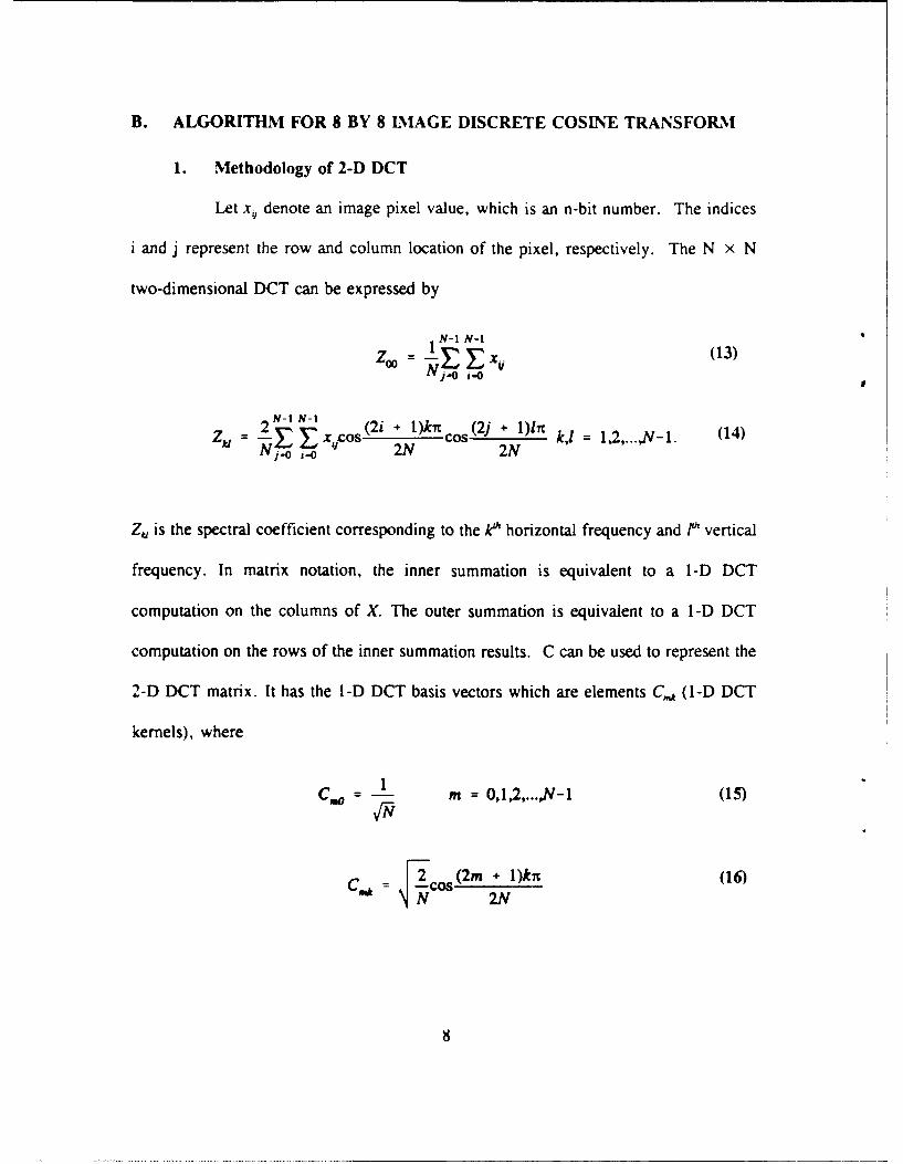
B. ALGORITHM FOR 8 BY 8 IMAGE DISCRETE COSINE TRANSFORM
1. Methodology of 2-D DCT
Let x,, denote an image pixel value, which is an n-bit number. The indices
i and j represent the row and column location of the pixel, respectively. The N X N
two-dimensional DCT can be expressed by
I N-i N-i
2 N-I NI + 1)kc (2j +I/inZ =s-0
+ ) s 2N s N kl = 1,2,...,N-1. (14)
Zk is the spectral coefficient corresponding to the k' horizontal frequency and I' vertical
frequency. In matrix notation, the inner summation is equivalent to a I-D DCT
computation on the columns of X. The outer summation is equivalent to a I-D DCT
computation on the rows of the inner summation results. C can be used to represent the
2-D DCT matrix. It has the I-D DCT basis vectors which are elements C,,k (I-D DCT
kernels), where
C 1 m = 0,1,2,...,N-1 (15)
FY,(2m + 1)kn (16)CNA J 2N

m = 0, 1, 2 ... , N-i; k = 1, 2, .... N-1. Because the kernels of the DCT
transformation can be separated, the 2-D matrix Z of 2-D DCT coefficients can be
represented as
Z = [X C]C = C'XC. (17)
This process can be realized in an architecture shown in Fig. 1 (referred to Ref. 11).
0-1.-01-2-D
1-0" 0 XI 1-Ocr
/g. 8 2-DThe N xmNock oOCT CeffD CT
6I1 6I4 W~rd 6I1
is te rno forPS te c1 -D DrT
12 COWe is can raw)
d41 Al TRAM84 dCxl.2
Fig. I 2-D DCT Block Diagram
The N x N block of image X is input column by column first, and the 1-13 DCT
computation is done. This computation is carried out as shown in the square bracket of
Eq. (17) for the j' column (for j = 0, 1, ... , N - 1). The rcsult of this N x N matrix
is then transposed for the second row by row I-D DCT computation. This transpose is
9

done as described by term on the outside of the square brackets in Eq.(1 7 ). After the
transposition, the same 1-D DCT computation involving the same transform matrix C is
carried out again. The transpose step takes care of the column to row change operations
of the data. The key operations involved here are the matrix transpose and the 1-D DCT
computation.
2. Principle of distributed arithmetic
The implementation of the 1-D DCT studied here is based on the principle
of distributed arithmetic. Using this principle, it is possible to implement the "bit
calculation" into the chip design. "Bit multiplication" is simply carried out by using the
input data bit pattern to address a Read Only Memory and by summing up all the results
to obtain the "transposed spectral values". If Y, (Y = (y" , Ni) is the image pixel vae
represented by a row vector, then its l-D DCT is
Nt-I
Z ,, = E y ,,C ,,, i~k = 0 , 1,- ... , - 1. (18 )
M-0
Now the input data y,, can be represented in 2's complement notation with
p-bit as
p- 2
Ym,= .,( - + , 2 (19)q-0
where y,,.q' is the q1 bit of the incoming image pixel values y,,. which have a value of
either 0 or 1. 2q is the binary weight of the q' bit. For example, if the input data is a 2's
10

complement 8-bit pattern then v,, = -y,,.,(7) x 27 + y O) x 20 + y,,(' x 21 + ym:'z x 22
+ V ,) x 23 + V" x 24 + y ,5) x 25 + y,,.,6) x 26. Substituting Eq. (19) into Eq. (18)
N-I p-2 N-I-E. cEk'-2- cyq2 (20)M-O q-O M-O
p-2Zk =-Fkt(Ckyi Y )2'P F (Ck y
q=O
where Fk is a function of the vectors Ck and Y'q) and is represented as
N-IFik(C~ylq) " (q ) (2F ,,(CkY~q)) = ,, for q = 0,1,2,..., p-1. (22)
M-0
Its binomial form can be shown as
(q, J ¢oy) (qy[) (q) (3
F 0 Yj + W. (23),kyq)= ~yio + "'"7 + CN-I.A.iN-I
where, q = 0, 1 ... , p-1.
3. Methodology for forming the ROM storage
In Eq.(23), c,, are 1-D DCT basis (kernels) vectors used as multiplication
coefficients. They are converted from decimal numbers to the 2's complement notation
used in this thesis. y,ql are the bit patterns represented in 2's complement form of the
N data points y,. Because the basis vectors are fixed value coefficients and Ft are
functions of the basis vectors and the binary bit patterns, the values of F, (with a fixed
II

k) for all possible N bit patterns (y ,,q,. m = 0, 1, 2, ... , N - 1) can be calculated and
stored in Read Only Memory (ROM) according to Eq.(22) and Eq.(23). The N-bit
pattcrn changes with time according to the incoming data V,,,q, (m = 0, 1, 2,..., N-i).
This bit pattern will form an address to access the ROM to extract the corresponding
F,,(Ck, Yq,) value.
From Eq.(20) and Eq.(2 1), the corresponding 1-D DCT spectral coefficient
Z,k can be computed by shifting and adding the F, values stored in the ROM. In Eq.
(2 1), Fk is a function of the corresponding basis column vector Ck for k = 0, 1, 2,.
N-1. Fa is different from each other as k varies. The incoming data vector Y, is the same
for the multiplication coefficients involved tor all values of k. It is possible to build up
N separate memory banks of multiplication coefficients and compute the N 1-D DCT
spectral coefficients Z, (k = 0, 1, 2,..., N-1) in parallel or concurrently.
4. Exploiting the synmetry in DCT to save storage in ROM
Here, 8 x 8 image blocks are used, so N = 8. The incoming data has 8 bits.
This means 2' = 256 possible bit patterns will be formed into addresses. There shall be
256 corresponding multiplication coefficient sum stored in the ROM for each of the 8
DCT spectral coefficients. However, advantage can be taken of the symmetry in the DCT
basis vectors. It can be shown that
C. = CN_,_,,, for k = 0,2,...,N-2 (k even). (24)
For example,
12

C -2Cos-2n ! 30 = C72 (25)Co2 : 8 16 8 16
where c,, is defined by Eq. (15) and Eq. (16). And the following can be proven,
C k = -Ct_,..t for k = 1, 3, ..., N-I (k odd) (26)
For example,
2 s 15n = -C71 (27)8 16 16
Hence, Eq. (18) can be reduced to
Nfl -
Z= (yin + y,&,_l..)Cmkm-0
where k = 0, 2,..., N-2 (k even) (28)
and,
13

N/2-1
Zi (yM - i-M)kM-0
where k = 1, 3,..., N-i (k odd). (29)
Equations (22) and (23) then can be reduced to
Nr2-I
Ft(Ck, Y(q) = E Ck(yi.+ Yi-,-V1 )(q))n--O
where k = 0, 2, 4,..., N-2 (30)
N12-1F= E . __.)
M-0
where k = 1, 3, 5 N-1. (31)
From the above equation-, it is possible to add or subtract the incoming data
points before memory access and reduce the number of distinct data values in ROM from
N to N/2. The total number of bit patterns is now only 2 /2 = 24 = 16. Only a 16 word
ROM is necessary for each of the 8 DCT coefficients, and therefore a total of 16 x 8
= 128 word ROM is required. This savings of ROM storage is significant compared to
the cost of using adders and subtractors in a different architecture. Since there is only
one particular bit pattern (those bits which have the same binary weight) at a time
allowed to address the ROM, and bit pattern changes according to the serially coming
14
data, the addition and subtraction can be done in a bit serial fashion. This advantage is
exploited in the chip implementation discussed in the next chapter.
15

M. A STRUCTURAL ARCHITECTURE FOR THE 1-D DCT
A. 8 x 8 IMAGE BLOCK 1-D DCT CIRCUIT ARCHITECTURE
The 1-D DCT architecture studied previously is shown in Fig. 2 [Ref. 1]. There
ck UM 4 jS aft" .
. 21. O"
Fig ft 1rhiecur it 1-D LOW
are 8 slices parallel to each other corresponding to the 8 DCT coefficients which are
computed concurrently. First, 12-bit pixels AI(1 1:0) are put column by column into the
serial-in-parallel-out" shift register (A). This sequence needs 8 clock cycles to complete.
16
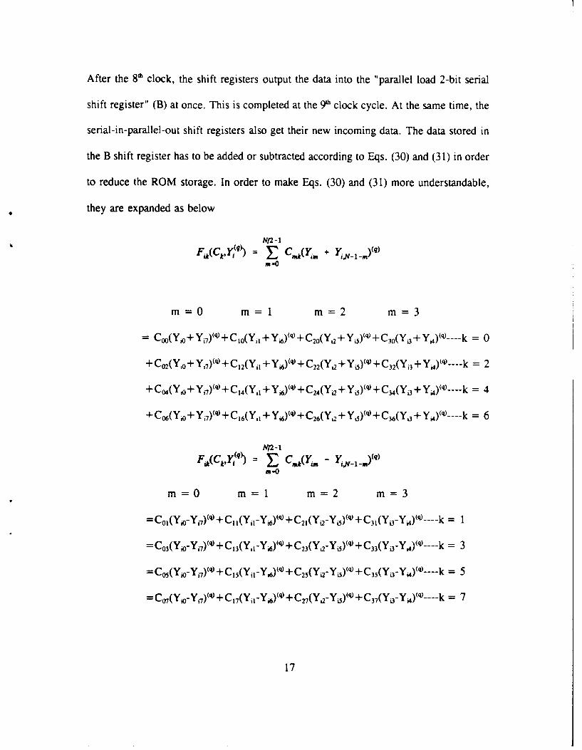
After the 8' clock, the shift registers output the data into the "parallel load 2-bit serial
shift register" (B) at once. This is completed at the 9' clock cycle. At the same time, the
serial -in-parallel-out shift registers also get their new incoming data. The data stored in
the B shift register has to be added or subtracted according to Eqs. (30) and (3 1) in order
to reduce the ROM storage. In order to make Eqs. (30) and (31) more understandable,
they are expanded as below
i _~ , 1_.)(q)rn-0
M =0 m=1 i= 2 mn= 3
=COO(YiO + y 7)(q)+ C 1 (Y1, + yi)() +C 20(Yi2+ y)')+ C30(Y 3 + Y) ---k =0
+ CO,(Yi 0+ y 7)( + C12(y1, + yi)) + C22(Y,2+ yi)(q + C32(Yi3 + YA4)(q---- k = 2
+ CO(Y, 0+ y,7)(4 + C14(y,1 + Y,)(l) + C24(yi2+ Y,)() + C3(Yi3+ Y,)(q) ---- k = 4
+ Cc6(Yj+ y.)(ql)+ C16(Y, + yi)(l) + C26(Y + yi5)(q + C36(Y,3 +yi)q ----k = 6
N12 -1
Fik(Ck yq -k~ iMj_)(q)
rn 0 m I m 2rn =C
= C01(Y-y 7)(" + C, ,(yi,-y 6 )(q + C21(Yi2-Yi)(q + C31(Yi3-YA4)(q---- k= 1
= C03(Yi-y 7)(q + CI3(yil-yi)('q+ C23(Y.2Yi~5)(q) +C33(yi3-y,) Y ---- k = 3
= CO(Y,-Y 7)(" + C,5(Yi1 -Y,)'" + C25(Y,2-Y.)('q+ C35(Y,3-Y,4)(q)---- k = 5
=CO+ ,7(Y ,,y7()+I(i-Y,6)"'q + C2'(yi-Y)('+ C37(YYi(q --- = 7
17

The numbers above the expanded equation represent the index m, and the numbers on
the right side are the index k. C, are multiplication coefficients. The bit
addition/subtraction is determined according to whether k is an even or odd number.
Registers B must be emptied in less than 8 clock cycles in order to receive new
Jata coming from registers A. Each datum is 12 bits in length. If a single bit is coming
out of registers B, it will take 12 clock cycles to empty the register. This will cause
collision during the addition and subtraction of the data. There are two ways to solve this
problem ; either to clock register B ,wice as fast or to shift out data 2 bits at a time. The
latter alternative has been chosen for the reasons of convenient design and easy system
considerations. The shifted 2-bit data is added or subtracted in the "2-bit
adder/subtractor" C. Their output is stored in the shift registers D which split the least
significant bit and most significant bit (binary weight q = 0 and q = 1) into two output
lines.
Next comes the question as to where the output data of the adders and subtractors
should go to address the ROM. How should the values in the ROM be arranged? It is
shown in the above expanded equations that all the adder outputs which is designated as
(U0(0:3) and U1(0:3) (Refer to Fig. 2). They are the 4 bits patterns which are the sum
of the two adjacent bit YM,.I'@ q = 0 represents LSB bit and q = I represents MSB bit in
Eqs (20) and (21). (U0(0:3) and U1(0:3) should be multiplied by the coefficients C,,,,
where k = 0, 2, 4, 6. All the two adjacent difference output V0(3:0) and V,(3:0) should
be multiplied by the coefficients C,, , where k = 1, 3, 5, 7. As a result, the four adders
and subtractors output bit patterns form a 4-bit address to access the corresponding
18

accumulated sum of the coefficients C,,,, k = 0, 1 .... 7 which are stored in ROM E.
This step will accomplish the 1-D DCT coefficient multiplication. The output of the
ROM is first latched in register F, and then adder/subtractor G will calculate the sum of
the "2-bit" spectral coefficient values according to Eq (21). The LSB (q = 0) values are
shifted to the right one position and added to the q = 1 values. This addition will
continue until the last bit pattern (12') of the incoming column data. According to Eq.
(19), the incoming data have been represented in 2's complement notation, so the most
significant bit's value should be subtracted from all the previous summations. This is
done by changing the add/sub control line of G into subtraction at the clock cycle of the
last bit pattern for each column of data.
The 2-bit sum or difference results of G are stored into register H and then sent to
the accumulator I and J. The accumulator consists of one "16-bit adder" and a "shift
right 2-bit register". The value stored in ROM E is a 16-bit word. The 16-bit adder I
adds the previous 2-bit right shifted value (output of J) to the incoming value (output of
H). The resulting value then is output to J register to do the 2-bit right shift. This process
will accomplish the computation of Eq. (21) as index q varies from 0 to p-I in 2 bit
increments. One thing has to be noted with caution; the initial value in the shift right 2-
bit registers for every incoming column of data should be zero. Otherwise, the ?revious
column values would accumulate. To avoid this, just clear the shift right 2-bit register
at the beginning of the accumulation of every column group.
After 8 clock cycles, the accumulated values are parallel loaded into register K.
Similar to register A but in the reverse direction, register K puts out the I-D DCT
19

spectral coefficients column by column. These I-D DCT coefficients are then transposed
by the transpose RAM (TRAM) according to Eq.(17). The transpose RAM is described
in the next section. After the transpose RAM, 1-D DCT coefficients are then input into
again the same 1-D DCT architecture. The only difference now is that the registers A
and B have to be expanded from 12 bits to 16 bits for the second transform.
B. TRANSPOSE RAM ARCHITECTURE
According to Eq. (17), the purpose of the "transpose RAM" is to change the 8 x
8 1-D DCT coefficient block's columns into rows; and rows into columns. The
coefficient values are generated from the 1-D DCT architecture column by column.
First, these values are put into a RAM while the transposed values are written.
Therefore, the transpose RAM must have the capability of reading in the 1-D DCT
values and writing out the transposed values in the same cycle. How can tnis be done?
The coefficient values come out of the 1-D DCT architecture in serial order; the
0, 1, 2,..., 7 coefficients of the first column of the 8 x 8 block come in first and then
the 0,1,... 7 coefficients of the second column and the third column and so on. This
order is a long stream of coefficients 0,1,... 63 for each 8 x 8 image block. After
storing them in the RAM, the coefficients must be read out in groups of 8 values in the
order of 0, 8, 16,..., 56; 1, 9, 17,..., 57; 2, 10, 18,..., 58; 3, 11, 19,..., 59; 4, 12,
20,..., 60; 5, 13, 21,..., 61; 6, 14, 22,..., 62; 7, 15, 23,..., 63 to achieve the transpose
operation. In the same cycle, just after reading out the first block of transposed values,
the coefficient values of the second block can be written into those locations. It is just
20

like reading block 1_0 (first 8 x 8 block position 0) and writing block 2_0 (second 8 x
8 block position 0), reading block 1_8 and writing block 2_1, reading block 1_16 and
writing block 2_2, and so on. In order to achieve the transpose of the second block, the
sequence for reading out block 2 must be in the order of 0, 1, 2,... 63. When reading
out the coefficients of block 2, the third block coefficients are being written into the same
locations just after read out. The order is just like reading block 2_0 and writing block
3_0, reading block 2_1 and writing block 31, reading block 2_2 and writing block 3_2,
and so on. Notice the sequential order is 0, 1, 2 .... 63 first, and then 0, 8, 16,..., and
then again in the sequential order of 0, 1, 2 .... 63, and so on.
As shown before the structural architecture design is based on the principle of
distributed arithmetic, and it is data-path oriented. The methodology to describe this
architecture in VHDL and to simulate it on a computer are discussed in the next chapter.
21

IV. VHDL BEHAVIORAL DESCRIPTION OF THE I-D DCT CONPONENT
A. BLOCK DIAGRAM DESCRIPTION
DII
C TEST BENCH
Fig. 3 -D DCT block diagram
The block diagram of the l-D DCT shown in Fig. 3 can be described in models
using VHDL. The block diagram shown here includes a 1-D DCT system discussed in
chapter III and the additional clock generators, delay lines, control line, package 1, and
test bench. There are minor differences between this diagram and the architecture
described in the previous chapter. What is taken into consideration when simulating this
22

system in VHDL is that a signal flow latency will occur. Therefore, a delay line is
necessary to change the clock triggering time and solve this latency problem.
Additionally, the architecture in the previous chapter does not make it clear when to
control the add/sub register G and fulfill the calculation of summing 2's complement
values. It is shown here that the control line generating this control bit is triggered by
the delayed clock.
From the modeling point of view, it is rather complicated to build up a 16-bit adder
in VHDL following the usual arithmetic logics. The easiest approach is to convert the
16-bit binary coefficient values into integer numbers and then do the addition or
subtraction in integers. After the integer addition or subtraction, the integers are simply
converted back to binary values. This conversion task is accomplished by functions in
package 1. A VHDL package is a collection of functions and procedures. Of course,
some overflow/underflow situations are expected to occur during these conversions. One
last thing to note in Figure 3 is that the test bench module controls all the signal flow,
the input data, and the output data, and it also simulates the whole design.
B. BI-TO-DI AND DI-TO-BI VHDL PACKAGE
the package 1 in VHDL is shown below,
package pack1 is -- Package declarationprocedure bi to in -- Procedure I changes 16 bits binary into integer
(variable x bit vector(15 downto 0);variable y out integer);
procedure in to bi --Procedure 2 changes integer into binary(variable m in integer;variable n out bit vector(15 downto 0));end packl;
package body pack l is -- Package body declaration
23
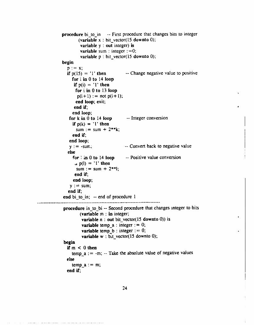
procedure bi to in -- First procedure that changes bits to integer(variable x bit_vector(15 downto 0);variable y out integer) isvariable sum : integer "=0;variable p : bitvector(15 downto 0);
beginp :=x;if p(15) = '1' then -- Change negative value to positive
for i in 0 to 14 loopif p(i) = '1' thenfor i in 0 to 13 loopp(i+ 1) := not p(i+ 1);
end loop; exit;end if;
end loop;for k in 0 to 14 loop -- Integer conversion
if p(k) = '1' thensum := sum + 2**k;
end if;end loop;y "= -sunm,; -- Convert back to negative value
elsefor . in 0 to 14 loop -- Positive value conversion
d p(l) = '1' thensum := sum + 2**1;
end if;end loop;
y • = sum;end if;
end bi to in; -- end of procedure 1
procedure intobi -- Second procedure that changes integer to bits(variable m in integer;variable n out bit vector(15 downto 0)) isvariable tempa integer'= 0;variable tempb integer'= 0;variable w bit vector(15 downto 0);
beginif m < 0 then
tempa = -m; -- Take the absolute value of negative values
elsetemp_a =m;
end if;
24

for i in 14 downto 0 loop -- Binary conversiontempb temp_a/(2**i);temp_a = temp a rem (2**i);
if (temp b = 1) thenw(i) ;= '1';
elsew(i) '0,;
end if;end loop;
if m > 0 thenw(15) = '0'; -- Assign positive sign bit
elsew(15) '1'; -- Assign negative sign bitfor k in 0 to 14 loopif w(k) = '1' then
for k in 0 to 13 loop -- Invert negative bits to 2's complementw(k+l) = not w(k+1);
end loop; exit;end if;
end loop;end if;if w(14)='0' and w(13)='O' and w(12)='0' and w(11)='0'and w(10)='O' and w(9)='0' and w(8)='0' and w(7)='0'and w(6)='0' and w(5)='0' and w(4)='0' and w(3)='O'and w(2)='0' and w(1)='0' and w(0)='0'thenw(15) '0'; -- Avoid negative zeroend if;
n w;end in to bi; -- end of procedure 2end packl; -- end of procedure
This VHDL package used in the simulation is basically similar to any other high-
level language subroutine involving specific shared operations. The difference here is
that it is possible to gather several different procedures or functions together in one
package. The packl here consists of two procedures -- bi to in and in to bi. Bitoin
converts the 16-bit binary numbers (represented in 2's complement notation) into positive
25
. . . . .. . . . . . . . . . . J

or negative integers. The in to bi procedure converts the positive or negative integers
back to 2's complement 16-bit binary numbers. Note that in the 2's complement number
system used here, there are only 16 bits including one sign bit. In overflow situations,
the digits that overflow will be truncated.
C. CLOCK GENERATOR MODULE (CLOCKGE)
The block diagram of the "clock ge" is shown in Figure 4.
The interface connection (port map in
VHDL) has also been shown. This tells
how the circuit can be connected to the
test bench. The VHDL source code of the
clk.vhd is shown below,
entity clockge is -- Entity-- declaration Fig. 4 clockge block diagram
port(CLCK :inout bit);end clock_ge;architecture clk_ctl of clockge is -- Architecture declarationbeginprocess(CLCK) -- Process declaration
variable I : integer = 0;begin -- Process beginCLCK <= not CLCK after 5 ns; -- Switching clock generationI:=I+ 1;assert I < = 80 -- Assertion terminates the infinite process
report "job done"severity Error;
end process; -- End of processend clk_ctl; -- End of architecture
There is a sensitivity signal "CLCK" in the source code which provides the clock
for all the circuits. The initial value of CLCK is "0." Its value is changed into "1" after
26

5 ns. Since a process in VHDL basically is an infinite loop, it is necessary to use an
"assert" instruction to terminate the process. By changing a counter value "I", the job
can be terminated appropriately after 80 iterations.
D. PARALLEL SHIFT REGISTER MODEL (LOAD).
LOAD
BO dO
Bi dlB2 d2
di Al B3 d3
clock ge B4 d4B5,- d5
B6,, d6
CLCK CLK 87 d
Fig. 5 Serial load parallel shift register block diagram
Figure 5 shows the detailed block diagram of the parallel shift register (LOAD).
The source code in VHDL is shown below
entity LOAD isport (Al : in bitvector(15 downto 0); B0,B1,B2,B3,B4,B5,B6,B7
out bit_vector(15 downto 0);CLK : in bit);end LOAD;architecture BEH of LOAD is
27

type shift is array (0 to 7) of bit_vector(15 downto 0);beginprocess
variable A : shift;variable I,count : integer = 0;
beginwait until CLK'event and CLK = '1'; -- Clock controls the timingfor count in 0 to 7 loop
wait until CLK'evet t and CLK = '1';for I in 0 to 6 loop -- f ush input values down to conect position
A(I) : = A(I+ 1);end loop;
A(7) := AI;if (count = 7) and (CLK'event and CLK='I') then -- Output data
BO < = A(7);BI < = A(6);B2 < = A(5);B3 < = A(4);B4 < = A(3);B5 < = A(2);B6 < = A(1);B7 < = A(0);
end if;end loop;wait on AI,CLK; -- Process activated when sensitivity signal changes
end process;end BEH;
The input 16-bit data come from Al column by column. The speed of the input data
is controlled by the test bench. Note that the first data that appears is the 8' pixel value
of the first column. In other words, the sequential order of the incoming data is 7, 6,
5,... 0. In this order, the data is pushed down into the correct position, and the 1-D
DCT can be done correctly. After the l-D DCT computation in Figure 3, the
corresponding spectral coefficients will be put back in the correct order,i.e., 0, 1, 2,...
7. "LOAD" module parallel outputs the data to the second circuit "SHIFT" after eight
clock cycles (count = 7). After that, it processes another new column of data.
28

E. SHIFT-TWO-REGISTER MODEL (SHIFT).
CK
SHIFT
dO - i0 boO Odl- il bol 1-0d2 -W2 Wo2 .W2
CLOCK DELAY d3 - M -00od4 -- 4 bo4 -w4d -WS o6 -SOSd8 - U boA -SWd7 - cub 7 ._=7
CLCK DE
Fig. 6 Shift two register block diagram
The block diagram for SHIFT is shown in Figure 6. There is the second clock
generator with three delay gates. Since the incoming pixel values pass through the
parallel shift register (LOAD), and it causes a delay of one clock cycle, it is necessary
to compensate for this latency by delaying the clock which triggers the shift-two-register
(SHIFT). Another clock which runs twice as fast as ck has been used to trigger the
original clock passing through the delay line. The VHDL source code of this faster clock
is similar to the previously discussed clock generator except the switching period is
twice as fast. The assertion time for termination is therefore twice as long. the delay line
29

consists of shift registers. The VHDL source code of the DELAY and the shift register
is as follows
entity delay isport(a :bit;b :out bit;CLK :bit); --Normal clock coming in from port
aend delay;architecture beh of delay is
beginprocess
variable x :bit;begin
wait until CLK'event and CLK = 'I'; -- Faster clock controls timingx := a; -- Shifting the incoming clock
wait on CLK,a;end process;
end beh;
entity shift isport(biO,bil,bi2,bi3,bi4,bi5,bi6,bi7: in bit -vector(15 downto 0);
bo0,bol,bo2,bo3,bo4,bo5,bo6,bo7: out bit -vector(I downto 0);CLK :in bit); -- Port declaration, eight input and output
end shift;architecture beh of shift is
beginprocess
variable I :integer =0; -- counter as well as indexbegin
for r in 0 to 7 loopwait until CLK'event and CLK = '1';boO(0) < = bi0(I); -- ""= 0 binary weightboO(1) < = biO(I+ 1); -- ""= 1 binary weightbol(O) < = bil1(1);bol(1) < = bi I(I + 1);bo2(O) < = bi2(I);bo2(1) < = bi2(I+ 1);bo3(0) < = Wi(I);bo3(l) < = bi3( + 1);bo4(O) < = bi4(I);bo4(1) < =bi4(I+l1);
30

bo5(0) < = bi5(I);bo5(l) < = bi5(I+l);bo6(0) < = bi6(I);bo6(l) < = bi6(I+l);bo7(0) < = bi7(l);bo7(l) < = bi7(I + 1);I := I + 2; -- increment of two
end loop;I : = 0; -- reset the counter for next column of datawait on CLK,bi0,bil,bi2,bi3,bi4,bi5,bi6,bi7; -- wait for new data
end process;end beh;
The data are input to the shift register in 16-bit words and output in 2-bit words.
Note that the counter "I" has been used as an index for each data word. Therefore, a
reset (I : = o) is necessary after each column of words are done. Otherwise, the index
would be running out of range, giving a run time error in the VHDL simulation.
F. 2-BIT ADDER/SUBTRACTOR MODEL (ADDSUB)
The 2-bit adder/subtractor module is shown in Figure 7. The "adsu" VHDL source
code is shown in Appendix A. A simple flow
chart in Figure 8 shows the behavior describedad
-W-,0 in VHDL. There are eight 2-bit words input
W' at IW ta -a into this circuit. It is necessary to do the
"4 0 W -"4WIm a4 bi as
s- d W -Me "serial" 2-bit addition or subtraction according.-- ~ k al ,wl
m7- dEI Ih7 .7
; I- to the expanded Eqs. (30) and (31). Since the
Fig. 7 2-bit add/sub blokdiagram incoming data have been presented in
31

2'complement notation, 2's complement
addition or subtraction should be used. On
the other hand, the 2-bit serial operation -w
should consider carriers generated , - :-
previously. In other words, the first 2-bit
addition/subtraction might generate a ,
Fig. 8 "adsu" flow chartcarrier. This carrier must carry on to the
next 2-bit add/sub computation. The simplest way to solve this problem is using a 2-bit
adder accompanied by a register handing the carrier bit for the next addition/subtraction.
For the subtraction case, it is necessary to convert the subtrahend into 2's complement
notation and then use the same 2-bit adder to accomplish the computation. What has been
done here is to convert the subtrahend into l's complement first and then add it to "1"
at the very first subtraction. The incoming subtrahend is just converted into l's
complement notation and the adder takes care of the "1" addition. In this way, the serial
subtraction is accomplished. There are four 2-bit adders and four 2-bit subtractors in the
source code. The "cr" bit sets the adder carry at the beginning to zero and the "st" bit
sets the subtractor carry to "1". Later on, the adder/subtractor will take care of the carry
by itself. For the convenience of notation, the incoming two 2-bit data and the carrier
bit have been combined into a 5-bit word, and the addition is done in the 2-bit adder
block. There will be more explanation as to how the 2-bit adder block is formed in the
later discussion.
32

G. SHIFT REGISTER
MODEL (REG)coO .aO bO -doO
The shift register block 001a bi dol
diagram is shown in Figure 9. o a22-d0
Signal is input from port a and C04- &4 Mb4 do4
output to port b. The shift register w _ sb o
model (REG) VHDL source code
is shown below
Fig. 9 shift register (reg) block diagram
entity reg isport(aO,al,a2,a3,a4,a5,a6,a7: bit -vector(1 downto 0); -- input port
bO,b l,b2,b3,b4,b5,b6,b7: out bit-vector(l downto 0); -- output portCLK :bit);
end reg;architecture beh of reg, is
beginprocessvariable dO,dl,d2,d3,d4,d5,d6,d7 : bit-vector(1 downto 0);begindO =aO; -- Substitute the input signal in a variabled I- al;d2 :=a2;d3 a3;d4 a4;d5 :=a5;d6 a6;V7 a7;wait until CLK'event and CLK = 'l'; -- Clock controlbO < = dO; -- shift the variable to output signalbi < =dl;b2 < = d2;bW < = d3;b4 < =d4;b5 < = d5;
33
b6 <= d6;b7 <= d7;wait on CLK;
end process;end beh;
This circuit is the simplest one. The only effect of this code is to use a signal
assignment statement to simulate a signal buffer causing a latency period of one clock
cycle. The "wait until CLK'event and CLK = '1';" statement activates the timing
control. The "wait on CLK" statement activates the process's operation whenever the
clock changes its state.
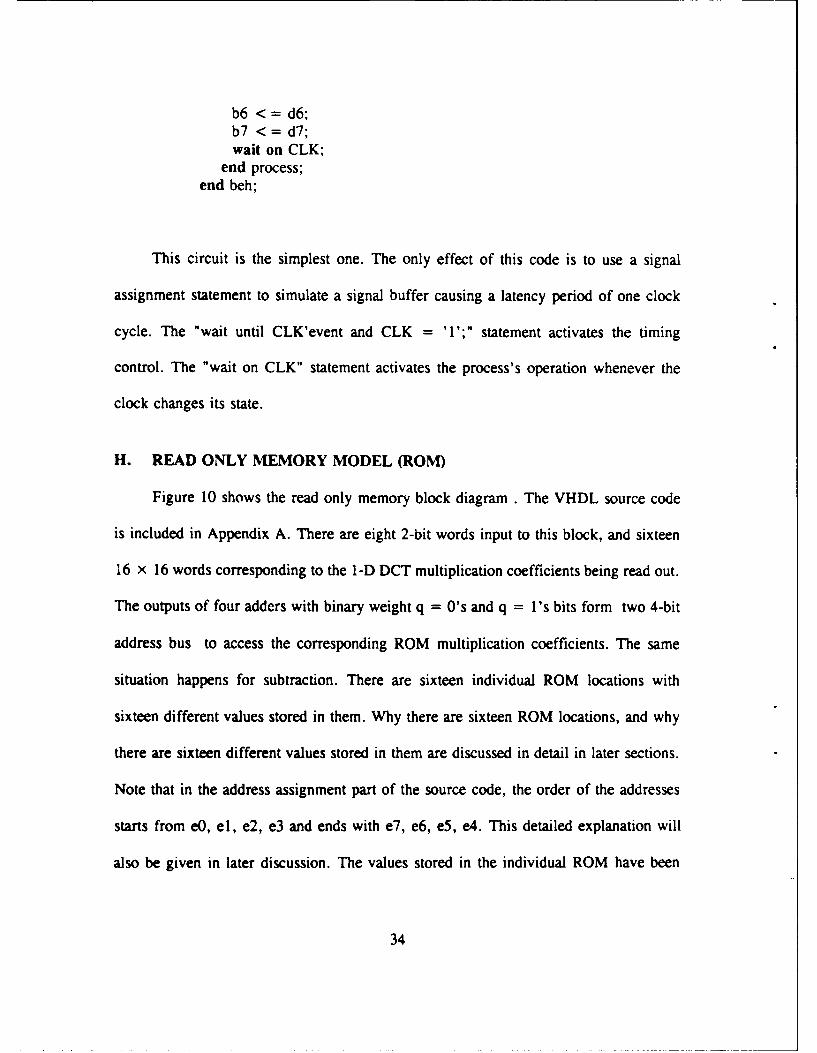
H. READ ONLY MEMORY MODEL (ROM)
Figure 10 shows the read only memory block diagram . The VHDL source code
is included in Appendix A. There are eight 2-bit words input to this block, and sixteen
16 x 16 words corresponding to the 1-D DCT multiplication coefficients being read out.
The outputs of four adders with binary weight q = O's and q = l's bits form two 4-bit
address bus to access the corresponding ROM multiplication coefficients. The same
situation happens for subtraction. There are sixteen individual ROM locations with
sixteen different values stored in them. Why there are sixteen ROM locations, and why
there are sixteen different values stored in them are discussed in detail in later sections.
Note that in the address assignment part of the source code, the order of the addresses
starts from eO, el, e2, e3 and ends with e7, e6, e5, e4. This detailed explanation will
also be given in later discussion. The values stored in the individual ROM have been
34

romblO el
dO - eO bl I e2b20 "--2 e3
dol el b21 .4bW ,--O e5
do2 e2 b31 eb40 e7
do3 e3 b41 e8d04 e4 b50 eg
b51 e0
do5 e5 b60 e12b8)1 o 12
do6 e6 b70 e13b71 e14
do7 e7 bSO el5CLK b1811 o11
IckFig. 10 ROM block diagram
converted from the sum of coefficients "Ck" to 16-bit 2's complement binary values.
The values of "Ck" are calculated according to Eq. (15) and Eq. (16).
I. SHIFT RIGHT I-BIT REGISTER MODEL (SHI_1)
Figure 11 shows the shift right 1-bit register block diagram. Its VHDL source code
is included in Appendix A. The shift right 1-bit register receives sixteen 16-bit words and
makes the right shift operation in eight words. It outputs the resultant sixteen 16-bit
words to the next circuit. The only difference between the input and the output values
is that the odd numbered 16-bit words have been shifted right 1 bit position. At the same
time, the original 16" bit (sign bit) of each odd word has been checked and replaced by
35

shl_1el fl blO fle2 f2 bll f2e3 f3 b20 f3e4.-- 4 b21 -4- ft5 5 b30 f5
e6 -0 f6 b31 f67 7---o b40 f7
98 f8 b41 f8g f9 b5O f9
elO flO b51 10ell -, fl1 b60 .-.f fll
e12 f12 b6l 12e13 13 b70 f13e14 f14 b71 fl 4e15 f15 b80. f 15e16 16 CLK b81 f 16
Fig. 11 Shil register block diagram
a proper bit ("0" or "1", depending on weather it has a positive or negative value) to
properly extend the binary 2's complement number.
J. ADDER/SUBTRACTOR-G MODEL (ADDG)
Figure 12 shows the addg block diagram. It includes one control circuit and five
delay gates. The control circuit enables the addg to do addition or subtraction. The
purpose of the delay line is to compensate for signal latency. To activate the add/subtract
controller at the right time when signal arrives is a required procedure.
36

ONTROL DELLAY PACKI
t @"subadd~gCk k t.a
bi g3
%-- as
16-- el bI .9
f7-- e1.7 Pq
fl-i 612 C94
Fig. 12 Addg block diagram
The addg VHDL source code as well as the control and the delay VHDL source
code are shown below.
entity control isport(CLK : bit;ct : out bit);
end control;architecture beh of control is -- control
beginprocess
variable i :integer =0;
beginwait until CLK'event and CLK ='I1'; -- Clock triggers the circuitif i = 7 thenct <= 1;- output '1' every eight clock periodelse
ct < = V0;end if;
i+ 1
37

if i =8 then= 0; -- Reset the counter
end if;end process;
end beh;
entity delayl10 isport(a : bit;b :out bit;CLK :bit);
end delay 10;architecture beh of delay 10 is -- delay
beginprocess
variable x :bit;beginwait until CLK'event and CLK = '1';x :=a;
wait on CLK,a;end process;
end beh;
use work.packl.all; -- All the functions in pack]. are usedentity addg is
port(al ,a2,a3,a4,a5,a6,a7,a8,a9,alO,aIl ,a12,al3,a14,a15,a16:bit -vector(15 downto 0); -- input portbi ,b2,b3,b4,b5,b6,b7,b8: out bit vector(15 downto 0); -- output portCLK,as :bit);
end addg;architecture beh of addg is
beginprocessvariable xl 1,x2, x3, x4, x5, x6, x7, x8, x9,xl10, x 11 ,x12, x13, x14, x15, x16,
nl,n2,n3,n4,n5,n6,n7,n8 : bit vector(15 downto 0);variable yl ,y2,y3,y4,y5,y6,y7,y8,y9,ylO,yllI,yl2,yl3,yl4,yl5,yl6,
m1, m2, m3, m4, m5, m6, m7, m8: integer =0;
beginwait until CLK'event and CLK = 'I';xlI al1; x2 a2; x3 a3; x4 :=a4; -input valuesx5:=a5; x6:=a6; 07:a7; x8:=a8;x9:=a9; xlO:=alO; xl. :all; x12:=a12;x13 :=a13; x14 :=a14; x15 :=a1.5; x16 :=a16;
-- Procedure call to do integer conversionbi-to-in(xl ,yl);bi to in(x2,y2);bi to_in(x3,y3);bi~to-in(x4,y4);
38

bi to in(x5,y5);bitoin(x6,y6);bitoin(x7,y7);bitoin(x8,y8);bi-to-in(x9,y9);bi to in(xl0,yl0);bi to in(xlIl, ylIl);bi to in(xl2,yl2);
bi to_in(x13,y13);bi to in(x14,y14);bito_ in(x15,y15);bito-in(x16,y16);if as '0' thenml yl + y2; m2 y3 + y4; m3 y5 + y6; m4 y7 + y8;m5 y9 + ylO; m6 yll + y12; m7 y13 + y14; m8 y15 +
y 16;else -- Control gives the subtraction instructionml yl - y2; m2 y3 - y4; m3 := y5 - y6; m4 y7 - y8;m5 y9 - yl0; m6 yll - y12; m7 y13 - y14; m8 y15 - y16;end if;-- Procedure call to do binary conversion
intobi(ml,nl); in to bi(m2,n2); into bi(m3,n3); into bi(m4,n4);intobi(m5,n5); in_to_bi(m6,n6); intobi(m7,n7); in_tobi(m8,n8);bI <= nl; b2 <= n2; b3 <= n3; b4 <= n4;b5 <= n5; b6 <= n6; b7 <= n7; b8 <= n8;wait on al,a2,a3,a4,a5,a6,a7,a8,a9,alO,all,al2,al3,al4,al5,al6,CLK;
end process;end beh;
The control is triggered by the clock, and an output of the control bit "ct" is
generated. On the 8' clock period, the "ct" becomes "1" but equals "0" otherwise. The
delay is also triggered by the clock. It receives one bit and outputs the same bit one clock
cycle later.
Addg has sixteen 16-bit word inputs and eight 16-bit word outputs. It performs
16-bit addition or subtraction. As discussed previously, it is rather complicated to build
up a 16-bit adder/subtractor in a VHDL structural approach. The easiest way is to
convert the 16-bit binary words into integers. In this way, "use work.packl.al" at the
beginning of the entity has to be declared, in order to call the "bi to in" procedure in
packl. "Work" represents the working library used, and "packl.all" represents all the
packages being used. After the conversion of binary values to integer values, addition or
subtraction was done according to the control input "as". The results then are converted
39

back to binary values again for output. Of course, the timing is always synchronized by
the clock.
re.hK. SHIFT REGISTER-H MODEL
gl aO bO hl
(REG-H) g2 al bl h293 a2 b2 h3
The regh block diagram is g4 a3 b3 h4g5- a4 b4 h5
shown in Figure 13. It functions just go. &5 b5 h
g7. a6 b - h7like "reg", except "reg" handles 2-bit g-- a7 cLK b7 -h8
words and "regh" handles 16-bitFig. 13 Shift registerg block diagram
words. The VHDL source codes are
the same except for the declaration of the length of bit-vectors.
L. 16-BIT ADDERI MODEL (ADDI)
Figure 14 shows the block diagram of the 16_bit adder (ADDI). ADDI and
ADD_G are basically the same. ADD_I does not have the "as" control bit or "if'
instruction in the VHDL -ource code to do the subtraction. Another big difference is
that ADD_I is not triggered by the clock. It adds up the two 16-bit inputs with no delay.
It does integer addition with the procedures in packi also. The two inputs come from
REGH and the feedback output from the SHI_2, which shifts the result to the right by
2 bits. This is shown in Figure 2. The VHDL source code for ADDI is shown below
use work.packl.all;entity add i is
port(al ,a2,a3,a4,a5,a6,a7,a8,a9,alO,al 1,al2,al3,a14,a15,a16:bit vector(15 downto 0);bl,b2,b3,b4,b5,b6,b7,b8 : out bit_vector(15 downto 0));
40

hl -dd iPACKi
Fig 14 16bit ad12 bokdiga
end add i; 1arhtetr -e ofadlli
Fig.,n314,n56 ,n7,n8d- bciagctram ont )
architecture6,mm8 intge 0;ad-iibegin
v9a 9:bl xlO alO: x4 xli a7,8,9lxl 2 a2,x3x4x5x6
x1I a 1; x4 a; xa;5 x a ; 6
hi -to_in(xl,yl);bi_to_in(x2,y2);bi_to_in(x3,y3);bi_to_in(x4,y4);bi -to_in(x5,y5);bi_to_in(x6,y6);bi_to_in(x7,y7);bi_to_in(x8,y8);bi -to_in(x9,y9);bi_to_in(xlO,ylO);bi_to_in(xl l,yll1);
hi -to_in(x13,y13);bi_to_in(xl4,y14);bi~to~in(xl5,yl5);
41

mlI yl1 + y2; m2 y3 + y4; m3 y5 + y6; m4 y7 + y8 ;m5 y9 + y1O; m6 yllI + y12; m7 yI3 + y14 ; m8 yl5
+ yl16;in_to_bi(ml,n 1); in_to_bi(m2,n2); in_to_bi(m3,n3); in_to_bi(m4,n4);in_to_bi(m5,n5);, in_to_bi(m6,n6); in_to_bi(m7,n7); in to bi(m8,n8);b I < = n I; b2 < = n2; b3 < = n3; b4 < = n4;b5 < = n5; b6 < = n6; b7 < = n7; b8 <= n8;wait on al ,a2,a3,a4,a5,a6,a7,a8,a9,alO,aIl 1,a12,a13,a14,a15,a16;
end process;end beh;
M. SHiff RIGHT 2-BIT REGISTER MODEL (SHI_2)
shl_2
al 30 riCLOCK DELAY Wr3
12 a2 sr4 r4US r5
13 &3 ,6 r6CK WS7 r7
b2 J2
b4--e1
b6 4-6I8.1 8 b7 -0-7
CLOK cLKcdr b8 A8
____ho Icr
Fig. 15 Shift right 2-bit register block diagram
The shift right 2-bit register (shi_2) block diagram is shown in Figure 15. It
includes another clock generator running two-times faster to trigger the delay unit which
delays the normal clock by one period. It has another clear line (clr) from the test bench
42

that clears the register every eight clock cycles. The VHDL source code of SHI_2 is
shown in Appendix B.
The SHI_2 model has eight 16-bit word inputs from ADD_I and has sixteen 16-bit
word outputs. The input values have been checked for the sign bit, and the SHI_2 shifts
the data 2 bits to the right in proper 2's complement representation. There are eight
blocks in the SHI_2 module. The results are updated and fed back to ADD_I module to
perform an addition with the incoming data values. In every 8' clock cycle, the results
are parallel shifted to the "parallel load serial shift" register (RESULT). During the same
cycle, the shift right 2-bit results are cleared, and the SHI_2 is ready for the next column
operation.
N. PARALLEL LOAD SERIAL SHIFT REGISTER MODEL (RESULT)
The block diagram of the parallel load serial shift register (RESULT) is shown in
Figure 16. There are eight inputs from SHI_2; RESULT puts out only one value at a
time. The VHDL source code of RESULT is shown below,
entity result isport(al,a2,a3,a4,a5,a6,a7,a8 : bitvector(15 downto 0);
k : out bit vector(15 downto 0);CLK : bit);end result;architecture beh of result is
type r is array (0 to 7) of bit vector(15 downto 0);begin
processvariable x : r;
beginx(0) al; x(1) a2; x(2) a3; x(3) a4;x(4) a5; x(5) a6; x(6) a7; x(7) a8;for i in 0 to 7 loop
wait until CLK'event and CLK = '1';
43

RESULT
J alJ2 a2J3 a3J4 a4 k PJ5 a5J6 a6J7 a7J8 a8 CLK
CCKFig. 16 Parallel shift serial output register block diagram
k <= x(i);end loop;
wait on al,a2,a3,a4,a5,a6,a7,a8,CLK;end process;
end beh;
Eight 16-bit words are input into RESULT every 8' clock cycle. They are pushed
out one value at a time at every clock period. After all eight values have been output,
new values are fed in again for the next cycle.
44

0. TEST BENCH
The Test bench block diagram is
shown in Figure 17. It actually TEST BENCH
dl dr set cr Pincludes all the intermediate signals, I IrI
the control signals, and the input and DESIGN CIRCUIT
output signals. The VHDL source code
for the test bench is shown in
Appendix B. All the components used
in the system have been declared and Fig. 17 Block diagram of Test Bench
instantiated. The signals used for the simulation are declared also. Configuration
statement binds all the components to the test system. The input pixel values are fed into
the system through "di", and it is simulated. The results of the simulation are collected
by signal "p". A table of the simulation results "p" is generated and analyzed to see if
the design is functioning correctly.
45
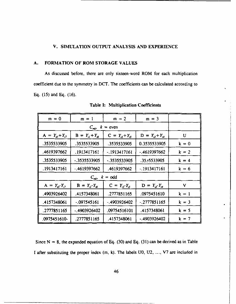
V. SIMULATION OUTPUT ANALYSIS AND EXPERIENCE
A. FORMATION OF ROM STORAGE VALUES
As discussed before, there are only sixteen-word ROM for each multiplication
coefficient due to the symmetry in DCT. The coefficients can be calculated according to
Eq. (15) and Eq. (16).
Table I: Multiplication Coefficients
m=0 m=1 m=2 m=3
C , k = even
A = YO+Y7 B = Y+Y C = Y2+Y5 D = Y.3+Y,4 U
.3535533905 .3535533905 .3535533905 0.3535533905 k = 0
.4619397662 .1913417161 -.1913417161 -.4619397662 k = 2
.3535533905 -.3535533905 -.3535533905 .35.i5533905 k = 4
.1913417161 -.4619397662 .4619397662 -.1913417161 k = 6
C,,, k=odd
A = Yo-Y7 B = Y1 -Yj C = Y,2- , D = Y,.3-Y,4 V
.4903926402 .4157348061 .2777851165 .0975451610 k = 1
.4157348061 -.097545161 -.4903926402 -.2777851165 k = 3
.2777851165 -.4903926402 .09754516101 .4157348061 k = 5
.0975451610- .2777851165 .4157348061 -.4903926402 k = 7
Since N = 8, the expanded equation of Eq. (30) and Eq. (31) can be derived as in Table
I after substituting the proper index (m, k). The labels UO, U2, ... , V7 are included in
46

the table for better understanding. Labels A, B, C, D stand for bit patterns. For example,
if A = 1, B = 0, C = 1, D = 1, then the values in column 1, 3, and 4 should be
summed up to get the corresponding multiplication coefficient sum stored in the ROM.
The bit pattern in the circuit has two weighted groups (LSB group q = O's, and MSB
group q = l's). The coefficient values for these two patterns are exactly the same.
Therefore, there are only 8 x 16 = 128 different coefficient sums stored in ROM.
One very important fact must be stressed. Are the values stored in the ROM
decimal numbers? The answer is obviously no. The values are stored in the ROM as
binary numbers. How can these summed decimal numbers be converted into binary
numbers? Upon inspection of Table I, it is noted that the largest possible decimal
number generated is not greater than 2. The smallest possible decimal number generated
is not lesser than -2. As stated before, the number system used here is 16-bit 2's
complement number. Therefore, one sign bit, one digit bit, and fourteen fraction bits are
chosen to represent the binary numbers stored in the ROM. All the decimal coefficients
calculated according to the specific bit pattern A, B, C, D have to be converted into
binary 2's complement 16-bit numbers. This conversion operation is carried out with the
help of a small program written in Matlab listed in Appendix C. The actual values stored
in the ROM are shown in the ROM VHDL source code.
B. SIMULATION AND TESTING IMAGE PATTERN (I)
The first image pattern being used is shown in Figure 17. It is a two-dimensional
cosine wave with intensity varied along x-axis. The pixel value can be represented in 128
47

7
6
3-
2
0 1 2 3 4 5 6 7
Fig. 18 Pattern (1) 8 x 8 image block
levels. Therefore, the pixel value of each point in this image can be represented from the
following formula
f (x, y) = [cos(2nf x + 2nf)+ 11/ 2 x 128 (32)
where f = 1/4,fy = 0.
After substituting the corresponding index (x, y) in Figure 17 into Eq. (32), the pixel
values represented in this 8 x 8 image block can be shown in Table 1I. The 12-bit binary
representations of decimal numbers 128 and 64 are "000010000000" and
"000001000000". Converting the values in Table II into 12-bit binary numbers and taking
48
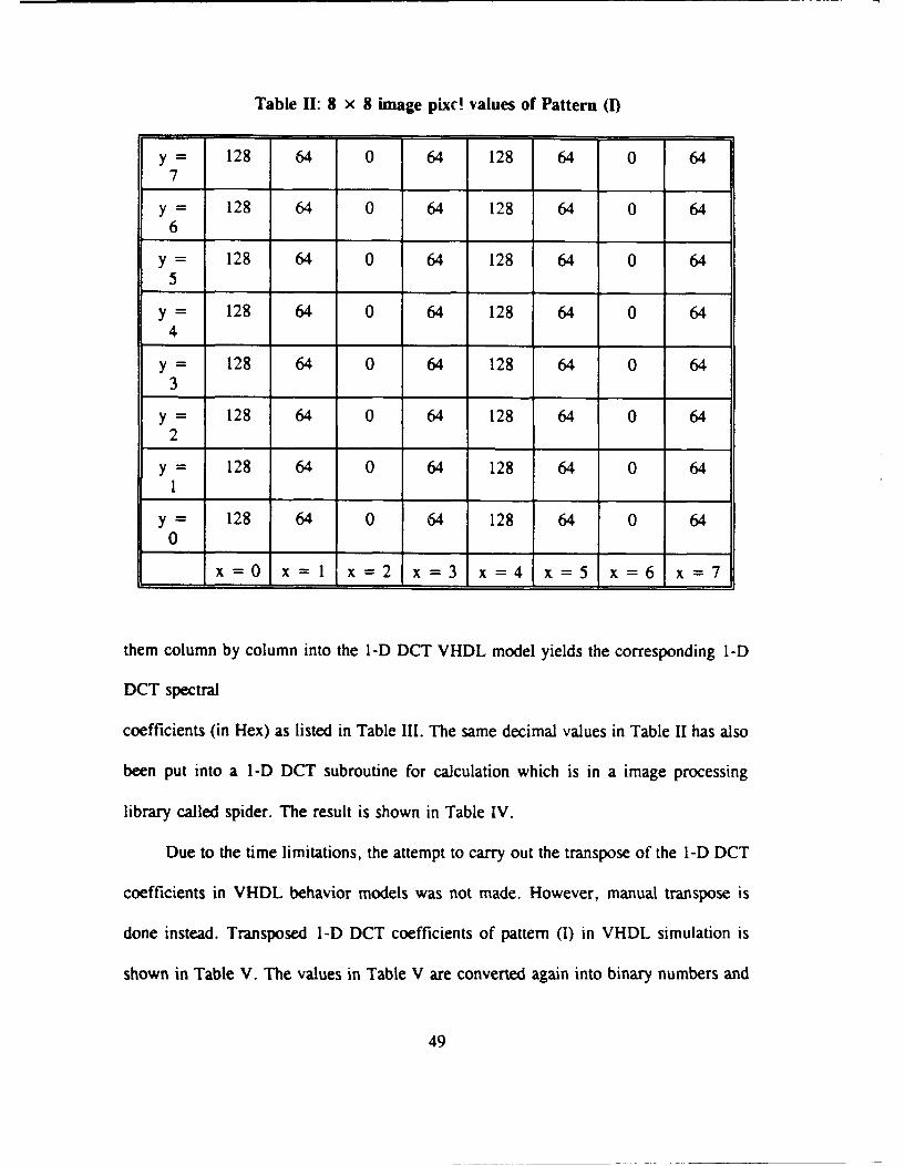
Table I: 8 x 8 image pixc! values of Pattern (I)
y 128 64 0 64 128 64 0 647
y = 128 64 0 64 128 64 0 646
y = 128 64 0 64 128 64 0 645
y = 128 64 0 64 128 64 0 644
y 128 64 0 64 128 64 0 643
y = 128 64 0 64 128 64 0 642
y = 128 64 0 64 128 64 0 641
y = 128 64 0 64 128 64 0 640
x=0 x= 1 x=2 x=3 x=4 x=5 x=6 x=7
them column by column into the 1-D DCT VHDL model yields the corresponding 1-D
DCT spectral
coefficients (in Hex) as listed in Table III. The same decimal values in Table II has also
been put into a I-D DCT subroutine for calculation which is in a image processing
library called spider. The result is shown in Table IV.
Due to the time limitations, the attempt to carry out the transpose of the 1-D DCT
coefficients in VHDL behavior models was not made. However, manual transpose is
done instead. Transposed I-D DCT coefficients of pattern (I) in VHDL simulation is
shown in Table V. The values in Table V are converted again into binary numbers and
49

Table 1H: 1-D DCT spectral coefficients of Pattern (1) in VHDL simulation
0B50 05A8 0000 05A8 0B50 05A8 0000 05A8
0000 0000 0000 0000 0000 0000 0000 0000
0000 0000 0000 0000 0000 0000 0000 0000
0000 0000 0000 0000 0000 0000 0000 0000
0000 0000 0000 0000 0000 0000 0000 0000
0000 0000 0000 0000 0000 0000 0000 0000
0000 0000 0000 0000 0000 0000 0000 0000
0000 0000 0000 0000 0000 0000 0000 0000
Table IV: 1-D DCT coefficients of pattern (I) using Spider Subroutine
362.03 181.01 0 181.0 362.03 181.01 0 1 181.011
0 0 0 0 0 0 0 0
0 0 0 0 0 0 0 0
0 0 0 0 0 0 0 0
0 0 0 0 0 0 0 0
0 0 0 0 0 0 0 0
0 0 0 0 0 0 0 0
0 0 0 0 0 0 0 0
input column by column into the 16-bit 1-D DCT VHDL model to accomplish the 2-D
DCT operation. The 2-D DCT spectral coefficients which have been transposed back in
the VHDL simulation are shown in Table VI. The I-D DCT operations in the VHDL
simulation is based on integer calculation. In order to prove that the 1-D DCT VHDL
50

Table V: Transposed I-D DCT coefficients of pattern (I) in VHDL simulation
0B50 0000 0000 0000 0000 0000 0000 0000
05A8 0000 0000 0000 0000 0000 0000 0000
0000 0000 0000 0000 0000 0000 0000 00000
05A8 0000 0000 0000 0000 0000 003 0000
0B50 0000 0000 0000 0000 0000 0000 0000
05A8 0000 0000 0000 0000 0000 0000 0000
0000 0000 0000 0000 000 0000 0000 0000
05A8 0000 0000 0000 0000 0000 0000 0000
Table VI: 2-D DCT spectral coefficients of pattern (I) in VHDL simulation
01F7 005F 0000 00C4 00FF FF7C 0000 FFED
0000 0000 0000 0000 0000 0000 0000 0000
0000 0000 0O0 0000 000 0000 0000 0000
0000 0000 0000 0000 0000 0000 0000 0000
0000 0000 0000 0000 0000 0000 0000 0000
0000 0000 0000 0" 0000 0000 0000
0000 0000 0000 0000 0000 0000 0000 0000
0000 0000 0 WW 0 0000 0000 0000
simulation result is correct, the values in Table V are converted into integers and are
shown in Table VII. The values in Table VII is again calculated column by column using
the spider I-D DCT subroutine. Its 2-D DCT spectral coefficients are transposed and
shown in Table VIII.
51

Table VII: Table V in integer values
2896 0 0 0 0 0 0 0
1448 0 0 0 0 0 0 0
0 0 0 0 0 0 0 0
1448 0 0 0 0 0 0 0
2896 0 0 0 0 0 0 0
1448 0 0 0 0 0 0 0
o 0 0 0 0 0 0 0
1448 0 0 0 0 0 0 0
Table VIII: 2-D DCT spectral coefficients of pattern (I) using Spider Subroutine
4095.5 768.54 0 1573.0 2047.7 -1051.0 0 -152.8
0 0 0 0 0 0 0 0
0 0 0 0 0 0 0 0
0 0 0 0 0 0 0 0
0 0 0 0 0 0 0 0
0 0 0 0 0 0 0 0
0 0 0 0 0 0 0 0
0 0 0 0 0 0 0 0
To ensure that the 1-D DCT structural calculation in the VHDL simulation is
correct , direct 1-D DCT calculation on a calculator is also carried out based on
Eq.(15), and Eq.(16). Equations (33) and (34) show the calculation example for k = 0
andk= 1.
52

1C(O) = -(28961448+0+1448+2896+1448+0+1448) (33)
C(1) = -(2896cos- + 1448cos- +0+ 1448cos-
8s 16 16 16
+2896cos9 il48os1 i+r 44c: 15nr (34)C(I44)os-++1448cos~
16 16 16
The results using this approach are listed in Table IX. Note that the results of Table VIII
and Table IX are very close.
Table IX: 2-D DCT coefficients of pattern (I) using direct calculation
4095.5 768.59 0 1537.0 2047.7 -1051.0 0 -152.8
0 0 0 0 0 0 0 0
0 0 0 0 0 0 0 0
0 0 0 0 0 0 0 0
0 0 0 0 0 0 0 0
0 0 0 0 0 0 0 0
0 0 0 0 0 0 0 0
0 0 0 0 0 0 0 0
It is also necessary to trace the operation in the VHDL structural models shown in
Figure 2. To understand the structural operation and calculation of the I-D DCT in the
VHDL simulation in more detail, a manual derivation and calculation are carried out for
53

Table X 16-bit binary number representation of table (V)
Slice(O) 0000101101010000 0 0 0 0 0 0 0
Slice(1) .00010110101000 0 0 0 0 0 0 0
Slice(2) 0 0 0 0 0 0 0 0
Slice(3) 0000010110101000 0 0 0 0 0 0 0
Slice(4) 0000101101010000 0 0 0 0 0 0 0
Slice(5) 0000010110101000 0 0 0 0 0 0 0
Slice(6) O 0000 00) 0 0 0 0 0 0 0
Slice(7) 0000010110101000 0 0 0 0 0 0 0
the purpose. First the values in Table V need to be converted into binary numbers, which
are shown in Table X. It is clear that only one column of Table X is not zero. Therefore,
there is only one column of the I-D DCT that needs computation. The values in the first
column are input into the 1-D DCT VHDL model which yields the serial 2-bit
addition/subtraction results as shown in Table XI.
The first column in Table XI shows how the 2-bit addition/subtraction is done. The first
row on the top represents the clock cycle. The rows in the upper-half (U) correspond
"k" equal to even numbers, and the rows in the lower-half (V) correspond "k" equal to
odd numbers. Each half column has four bits, forming a bus to address the corresponding
ROM coefficients. For example, at the first clock cycle, there are two 4-bit buses. The
four least significant bits (LSB) form an "ABCD" corresponding to "0000" bus to address
the "U00" (refer to Fig. 2) ROM value. This yields the value "0" as
output. The MSBs of the first clock cycle addresses the "U1J" ROM valur
54

Table XI: Serial 2-bit addition/subtraction output
Clcki- dock- lock - dock- dock- cdock T dlock-8_ 8 7 6 5 4 3
Slice (0+7) 00 01 00 00 11 11 10 00 A
Slie(1+6) 00 00 01 01 10 10 10 00 BU
SiOe(2+ 00 00 01 31 10 10 10 00 C
Slice (3+4) 00 01 00 00 11 11 10 00 D
Slice (3-4) 11 11 01 10 01 01 10 00 D
Slice (2-5) 11 11 01 10 01 01 10 00 CV
Slice (1-6) 00 00 10 01 10 10 10 00 B
Slie (0-7) 00 00 10 01 10 10 10 00 A
"0000000000000000" out. It then adds up with the 1-bit right shifted value of "UOO".
This result is stored in REGH and then 2-bit right-shifted in the SHI_2 register. The
first clocked 2-bit right-shifted word is then fed back to ADDI and added to the second
clocked result "0101101010000010". The procedure of getting this second clocked result
is just the same as that of getting the first clocked result. The summation of the first 2-bit
right-shifted number and the second clocked result "010110101000010" is then shifted
right 2 bits, yielding "0001011010100000". This value is then added to the third clocked
result "0111000100100010", yielding "1000011111000010". This process goes on
serially until the 8"' clock cycle is reached. The addressed output ROM value of the MSB
of the 8"' clock cycle "0" is subtracted from the right-shifted 1-bit
55

Table XH 2-D DCT coefficients of pattern (I) using manual calculation
ARANN MIMI 111! IOM 0110 M 11 DIX0000M 1AM00 0 ROn00 1M OD gnaw 1111111 11 t11"1111111t14 -- -O--- ........ 111|11tl1101l0
0 0 0 0 0 0 0 0
0 0 0 0 0 0 0 0
0 0 0 0 0 0 0 0
0 0 0 0 0 0 0 0
o 0 0 0 0 0 0 0
0 0 0 0 0 0 0 0
0 0 0 0 0 0 0 0
addressed ROM value of the LSB of the 8' clock cycle "0000000000000000". This result
is then added to the previous accmulated 7 clocked values, yielding
"0000011111111111". This final result is then right shifted 2 bits, yielding
"00000001 11111111" and output as the first pixel 2-D DCT coefficient of the first
column. 8 x 8 image block of the 2-D DCT coefficients pattern I using structural
manual calculations are shown in Table XII. The detailed calculation procedure is listed
in Appendix D. Note that the summation of the accumulated two clocked values and the
third clocked result generates an overflow. This overflow will eventually generate a
negative value when right-shifted 2 bits. This is a inherent drawback of using 16-bit
integers arithmetics.
56

C. SIMULATION AND TEST OF IMAGE PATTERN (H)
Image pattern II is equal to image pattern I rotated by 45°. The following formula
was used to calculate each pixel value.
f (x,y) = [cos(2it(n!jTx + 27t(#)7Y) + 11 / 2 x 128 (35)
Table XI: 8 x 8 image block pixel values of pattern (H)
[ 7 64 128 64 0 64 128 64 0
6 0 64 128 64 0 64 128 64
5 64 0 64 128 64 0 64 128
4 128 64 0 64 128 64 0 64
3 64 128 64 0 64 128 64 0
2 C 64 128 64 0 64 128 64
1 64 0 64 128 64 0 64 128
0 128 64 0 64 128 64 0 64
0 1 2 3 4 5 6 7
The 8 x 8 image block pixel values of pattern II represented in decimal numbers are
shown in Table XIII. The 2-D DCT of pattern II has been calculated in two ways,
VHDL simulation and spider subroutine. Using VHDL simulation first, Table XIII is
converted into binary numbers and is input column by column into the VHDL 1-D DCT
test bench. Its I-D DCT coefficients is shown in Table XIV. For 2-D DCT, the values
57

Table XIV: I-D DCT coeffiTients of pattern (I) using VHDL simulation
7 016A 016A 016A 016A 016A 016A 016A 016A
6 FFBB 0043 0043 FFBB FFBB 0043 0043 FFBB
5 0000 0000 0000 0000 0000 0000 0000 0000
4 FF74 008A 008A FF74 FF74 008A 008A FF74
3 00B5 00B5 FF4A FF4A 00B5 00B5 FF4A FF4A
2 005D FFA2 FFA2 005D 005D FFA2 FFA2 005D
1 0000 0000 0000 0000 0000 0000 0000 0000
0 OOOD FFF2 FFF2 OOOD OOOD FFF2 FFF2 000D
0 1 2 3 4 5 6 7
in Table XIV are then transposed manually, and the results are input into the 16-bit
VHDL 1-D DCT test bench. The 2-D DCT spectral coefficients fo ittern II in VHDL
simulation are listed in Table XV.
Table XV: 2-D DCT coefficients of pattern (IM using VHDL simulation
7 005F 0000 0000 0000 0000 0000 0000 0000
6 FFFF 0000 0000 0000 FFE7 0000 0000 0090
5 0000 0000 0000 0000 0000 0000 0000 0000
4 FFFF 0000 0000 0000 FFCE 0000 0000 0000
3 F555 0017 0000 0031 0000 FFDE 0000 FFFC
2 FFFF 0000 0000 0000 0020 0000 0000 0000
1 0000 0000 0000 0000 0000 0000 0000 0000
0 FFF 0000 0000 0000 0005 0000 0000 0000
0 1 2 3 4 5 6 7
58

Table XVI: Pattern H 1-D DCT coefficients using Spider Subroutine
7 181.0 181.0 181.0 181.0 181.0 181.0 181.0 181.0
6 -33.97 33.97 33.97 - - 33.97 33.97 -
33.97 33.97 33.97
5 0 0 0 0 0 0 0 0
4 -69.53 69.53 69.53 - - 69.53 69.53 -
69.53 69.53 69.53
3 90.51 90.51 -90.51 - 90.51 90.51 -90.51 -
90.51 90.51
2 46.46 -46.46 -46.46 46.46 46.46 - -46.46 46.4646.46
1 0 0 0 0 0 0 0 0
0 6.757 -6.757 -6.757 6.757 6.757 6 -6.757 6.757____ __ _ ____ __ ____ ____ _ __ ___ 6.757 _ _ _ _
0 1 2 3 4 5 6 7
1-D DCT subroutine in Spider is used to double check the VHDL simulation
result. Values in Table XIII are calculated column by column, and its result is listed in
Table XVI This result is compared with that of Table XIV for verification.
2-D DCT floating point calculation is also used to check the VHDL simulation.
Again for the same reason of comparison, values in Table XIV are chosen and converted
into integers. After the Hex-integer conversion, these values are transposed again and
calculated by 1-D DCT Spider subroutine column by column. The results are shown in
Table XVII.
59

Table XVII: 2-D DCT coefficients of pattern (H1) using floating point calculation
7 1023.9 0 0 0 0 0 0 0
6 -2.828 0 0 0 -192.3 0 0 0
5 0 0 0 0 0 0 0 0
4 -2.828 0 0 0 -393.2 0 0 0
3 -1.414 192.7 0 394.4 0 -263.5 0 -38.33
2 -1.414 0 0 0 264.5 0 0 0
1 0 0 0 0 0 0 0 0
0 -1.414 0 0 0 38.18 0 0 0
0 1 2 3 4 5 6 7
D. RESULT ANALYSIS
There are four methods being used to prove the accuracy of the VHDL structural
1-D DCT in 'vHDL simulation. Comparing Tables VI, VIII, IX, and XII, the
similarities among them are obvious. Tables VIII and IX are almost the same while
Tables VI and XII need to be converted into decimal numbers for ease of comparison.
Table VI needs to be converted into 16-bit binary values first, then using the definition
of the 16-bit binary number system (1 sign bit, 1 integer and 14 fraction bits) to convert
the binary words into decimal numbers.
The multiplication factor as to how many times the number is being right-shifted
here is 2' T. The equivalent integer values of Table VI and Table XII are shown in Table
XVIII and XIX. Most of the pixel values are similar to those in Table VIII and IX with
a few differences. There are two reasons that can explain this phenomenon. First, there
is a limitation in 16-bit binary number representation. Those fractional numbers that are
60

Table XVII Equivalent decimal numbers of table (VI)
4024 760 0 1568 2040 -1056 0 -152
0 0 0 0 0 0 0 0
0 0 0 0 0 0 0 0
0 0 0 0 0 0 0 0
0 0 0 0 0 0 0 0
0 0 0 0 0 0 0 0
0 0 0 0 0 0 0 0
0 0 0 0 0 0 0 0
Table XIX Equivalent decimal numbers of table (XI)
4088 760 0 1568 2040 -1056 0 -160
0 0 0 0 0 0 0 0
0 0 0 0 0 0 0 0
0 0 0 0 0 0 0 0
0 0 0 0 0 0 0 0
0 0 0 0 0 0 0 0
00 0 0 0 0 0 0
0 0 0 0 __0 0 0 0
smaller than 2t4 are truncated. This will cause small difference between Table VI,XII
and Table XVIII,XIX. The second reason is due to the overflow situation. The
accumulated sum of Che coefficients might be greater than the biggest number that a 16-
bit binary number system could represent. This overflow situation will cause larger
difference between Table VI,XII and Table XVIII,XIX.
61

A way is found to indicate the overflow situation. Checking can be made in
ADD_G and ADD_I by adding the following VHDL source code right after the integer
to binary number conversion.
if ((x(15) = '1' and x2(15) = '1' and n,(15) = '0') or
(x(15) = '0' and x2(15) = '0' and n(15) = '1')) then
overl <= '1';
if ((X3(15) - '1' and x,(15) = '1' and n2(15) = '0') or
(X3(15) - '0' and x,(15) = '0' and n2(15) = '1')) then
over2 < = '1';
if ((x 5(15) = '1' and x,,(15) = '1' and n,(15) = '0') or
(xls(15) = '0' and xl,(15) = '0' and n,(15) = '1')) then
over8 <- '1';
0" course, at the port declaration, a special signal declaration must be made in order to
notify the test bench about this overflow condition. VHDL source code for the port
declaration is shown below.
port(-;bl,b2,b3,b,bS,b6,b7,b8 : out bitvector(15 downto 0);
overl,over2,over3,over4,over5,over6,over7,over8 : out bit;
CLK : bit);
-ddition to the port modification, the test bench component's port also needs to be
modified, the last thing to accomplish in signaling this overflow condition is to declare
62

signals and unable the "port map" to receive the overflow signal coming from ADDG
and ADD I. VHDL source code is shown below.
signal ovl,ov2,ov3,ov4,ovS,ov6,ov7,ov8 : bit;
g: addg port map(fl,f2,f3,f4,f5,f6,f7,f8,f9,flO,fll,fl2,fl3,fl4,fl5,fl6,
gl,g2,g3,g4,g5,g6,g7,g8,ck,qo,ovl,ov2,ov3,ov4,ov5,ov6,vo7,vo8);
i addi port map(hl,rl,h2,r2,h3,r3,h4,r4,r4,h5,r5,h6,r6,h7,r7,h8,r8,
il ,i2,i3,i4,i5,i6,i7,i8,ck,ovl ,ov2,ov3,ov4,ov5,ov6,ov7,ov8);
Whenever the overflow bit "ov#" changes to '1', it indicates that particular pixel value
has experienced overflow.
E. EXPERIENCE
My experience in the work can be listed as follows.
1. Input Data Sequential Order error
The sequential order of input pixels which are input to the parallel shift
register was assumed to be 7, 6, ...0. According to the transposed sequence, the actual
input data should be in the order of 0. 1, 2,...7. Therefore, there would be an error if
the sequence of the transposed data is not reversed. This means that another reverse
circuit should be added between the transpose circuit and the input "load" circuit. But,
63

it is rather complicated to add an extra circuit. The easiest way to solve this problem is
to input the data in the order of 0, 1 .... 7 and switch the subtrahend connections (0-7, 1-
6, 2-5, 3-4) in the 2-bit adder/subtractor circuit. In this way, the order of input data and
output data are always in the order of 0, 1, 2,... 7 and it is not necessary to add an extra
circuit.
2. Formation of 2-bit Adder in VHDL source code
The interface of a 2-bit adder has five inputs (two for the adder, two for the
addend, and one for the carrier), three outputs (two for the addition result, and one for
the carrier). Thus, a truth table involving all possible input combinations can be made.
There are five inputs, therefore 2s = 32 combinations will occur. After building up an
8 x 32 truth table, Karnaugh map reduction can be used to minimize the complex
expression in boolean algebra. It is the boolean algebra expression which is used in the
VHDL source code. There is a detailed example listed in Appendix I.
3. No Timing control in Addi Model
Almost every circuit needs a clock to trigger and control the sequential
process. ADD I is a special adder circuit without a triggering clock. As mentioned
earlier, the accumulator of the serial bit result consists of ADD I and SHI 2. ADD I is
used to add up the incoming clocked result with the latest accumulated result right after
right-shifting by 2 bits. If these two circuits are triggered by the clock, then there will
be a time delay of one clock cycle between ADD_I and SHI_2. In other words, ADD_I
is adding the incoming clocked result with the accumulated right-shifted 2-bit result from
64

one clock cycle earlier, rather than the latest. This will cause an error in the output
coefficients. The method to remove of this time delay of one clock cycle between ADD_I
and SHI 2 is to allow only one clock to trigger this accumulator. Another alternative
considered is to use the clock to trigger ADD I instead of triggering SHI_2. However,
the experiment shows that this cannot be done, since SHI_2 has to be cleared on every
81 clock cycle, and this clearing needs a counter to calculate the exact time. On the other
hand, SHI_2 is to output the correct accumulated result every 8 ' clock period. These two
factors both need a clock to control the timing. This is why ADDI was chosen not to
be triggered by the clock.
4. "Set" control in Test Bench
It is strange enough that the "set" control in the test bench does not get the
value '1' at the beginning of simulation. The function of "set" is to initiate all the
subtractor's carriers in "adsu" to '1' in order to accomplish the subtraction. This
initiation is performed only once. The carrier of the subtractor is then carried over all
by itself. That is to say, the carrier is a variable in "adsu". This carry variable is initiated
by the "set" first and will be influenced by the "set" at subsequent times if modification
of the signal "set" is not made. Fortunately, "set" has to change only once from '0' to
'1 at the beginning of the simulation. Therefore, an "event" instruction causes "set" to
be a sensitivity signal. Since "set" changes only once, it will not have any further
influence on the carrier variable. Other than this, the time for "set" to change its state
is very important. the clock is '0' at the beginning of the simulation and changes its state
to '1' after 5 ns. If "set" changes its state other than at 5 ns, the subtraction result will
65

be wrong. Only when "set" changes its state at 5 ns will the result of subtraction be
correct.
5. Signals cannot be used as variables in VHDL
In solving the problem mentioned in previous section, efforts have been made
to use the "set" signal directly as a variable within the process. This certainly will yield
a syntax error doing compilation of the source codes.
6. Preventing Negative Zero occurrences in Packl
There is a paragraph of source code added to packl at the end of "in to bi"
when negative zeros found during the simulation. When these negative zeros arrive at the
gate of shi_2, they will generate very large negative numbers and cause an error at the
output. This unwanted situation has teen taken care of by adding source code to check
for negative zeros at the end of the integer-binary conversion procedure. Although this
exura checking source code works fine, it means an extra circuit must be added. This
is not the goal in circuits design. A close inspection of in tobi source code has been
made and a very small mistake has been found. At the beginning of inverting the bit
stream into 2's complement codes, positive or negative integers is checked in order to
assign the correct sign bit "w(15)" for the converted binary number. It is found that
"w(15) = '0" is only assigned to the situation when "m > '0"'. The other values are
all assigned with "w(15) '1"'. This is how negative zeros are generated. Had the
source code "m > '0'" been changed to "m > = '0'", the extra negative zero checking
codes would not be necessary.
66
VI. CONCLUSION
The main objectives of this thesis, using the VHDL to describe a 1-D DCT
structural architecture of a 8 x 8 image block and simulating it on a workstation, have
been reached. The basic theory of 1-D DCT, the principle of distributed arithmetic and
the actual hardware architecture have been made more clear in the VHDL simulation.
Above all, the experience of using the VHDL to describe an algorithm and the simulation
of the VHDL is obtained. Although getting familiar with the language and its simulation
has been time-consuming, the benefits of the signal tracing and the time modeling have
been demonstrated in this thesis. VHDL itself is a portable document and a hierarchical
language. Therefore, this thesis can be adopted in other more complicated design.
Despite the fact that the VHDL simulation result of integer point calculation is not
as precise as floating point calculation, the resultant energy spectrum of l-D DCT is
already good enough to recover the original image block. Besides, absolute value
accuracy is not important for image compression. It is the relative value between pixel
points that matters. Another point worthy to mention is that the approach in this thesis
has the advantages of calculation speed, since the hardware for floating point calculation
is much more complicated than that for integer point calculation.
There is still a very important module that waa not described, the transpose
module. The transpose module can be connected to the test bench and fulfill the
automatic 2-D DCT simulation.
67

The simulation done here is only the initial part of the "top-down design" process.
The algorithm of an 8 x 8 image block 2-D DCT in VHDL behavior description was
implemented. This behavior description can be further developed into gate level
descriptions. Once reached the gate level, the hardware circuit implementation can be
realized.
68
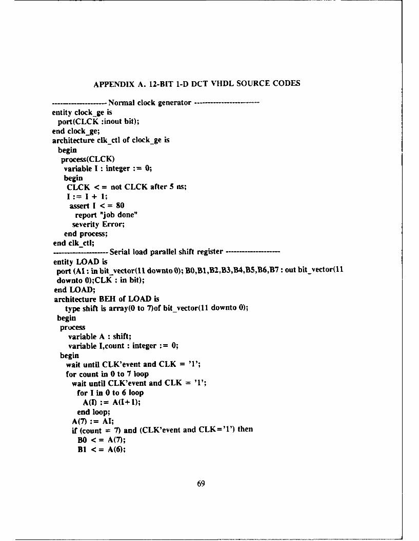
APPENDIX A. 12-BIT 1-D DCT VHDL SOURCE CODES
--------- -- Normnal clock generator ---- -----------
entity clock ge isport(CLCK :inout bit);
end clock ge;architecture cik-ctl of clock ge is
beginprocess(CLCK)variable I1: integer :=0;beginCLCK <= not CLCK after 5 ns;
:=+I1+assert I <= 80
report "job done"severity Error;
end process;end clk-ctl;
--- Serial load parallel shift register ----------entity LOAD isport (Al : in bit -vector(U. downto 0); BO,BI,B2,B3,B4,B5,B6,B7: outhit-vector(11downto 0);CLK : in bit);
end LOAD;architecture BEll of LOAD is
type shift is array(0 to 7)of bit-vector(11 downto 0);beginprocess
variable A : shift;variable I,count : integer : = 0;
beginwait until CLK'event and CLK = '1';for count in 0 to 7 loop
wait until CLK'event and CLK = '1';for I in 0 to 6 loop
A(I) := A(1+1);end loop;
AM7 := AI;if (count = 7) and (CLK'event and CLK='1') then
BO < = A (7);B1 < = A(6;
69

B2 < = A(5);B3 < = A(4);B4 < = A(3);B5 < = A(2);B6 < = A(1);B7 < = A(0);
end if;end loop;
wait on AI,CLK;end process;
end BEH;Twice faster clock generator
entity clock isport(CLK :inout bit := '1');
end clock;architecture beh of clock is
beginprocess(CLK)variable I : integer 0;beginCLK < = not CLK after 2.5 ns;I:= I+ 1;assert I < = 160
report "job done"severity Error;
end process;end beh;
Delay gate --..............entity delayl0 is
port(a : bit;b : out bit;CLK : bit);end delaylO;architecture beh of delaylO is
beginprocess
variable x : bit;begin
wait until CLK'event and CLK - 'I';x := a;b < =x;
wait on CLK,a;end process;
end beh;---------------- ---- Para llel shift out 2-bit register -------------------
70

entity shift isport (bi0,bi l,bi2,bi3, bi4,bi5,bi6,bi7: in bit -vector(11 downto 0);
bo0,bol,bo2,bo3,bo4,bo5,bo6,bo7: out bit vector(1 downto 0);CLK :in bit);
end shift;architecture beh of shift is
beginprocess
variable I : integer =0;
beginwait for 90 ns;for r in 0 to 5 loop
wait until CLK'event and CLK ='1';bo0(0) < = bi0(I;bo0(1 < = bi0(I+ 1);bol (0) < = bil(I);bol(1) < = bil (1+1);bo2(0) < = bi2(I);bo2(1) < = bi2(I+ 1);bo3(0) < = WM(I;bo3(1) < = bi3(I+ 1);bo4(0) < = WM(I;bo4(1) < = bi4(I+ 1);bo5(O) < = bi5(I;bo5(1) < = bi5(I+ 1);
bo6(0) < = bi6(I+ );
bo7(0) < = WM(I;bo7(1) < = bi7(I+ 1);I := I + 2;
end loop;
I :=0;wait on CLK,bi0,bil,bi2,bi3,bi4,bi5,bi6,bi7;
end process;end beh;
---- ---- 2-bit adder/subtractor----------entity adsu is
port (aO,al,a2,a3,a4,aS,a6,a7 : bit -vector(1 downto 0);b0,bI,b2,b3,b4,b5,')6,b7: out bit-vector(1 downto 0);CLK,cr,st : bit);
end adsu;
71
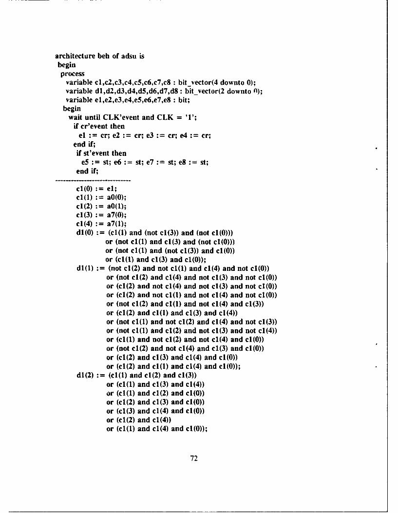
architecture beh of adsu isbeginprocess
variable cl,c2,c3,c4,cS,c6,c7,c8 :bit_vector(4 downto 0);variable dl,d2,d3,d4,d5,d6,d7,d8: bit -vector(2 downto 0);variable el,e2,e3,e4,e5,e6,e7,e8 : bit;
beginwait until CLK'event and CLK = '1';
if crevent thenel : = cr; e2 :=cr; e3 :=Cr; e4 :=cr;
end if;if st'event then
e:= st; e6:=st; e7 : =st; e8:=st;end if;
WlO) el;
c1(2) :=aO(1;
cl(4) a7(1);dl(O) :=(c][0) and (not cl(3)) and (not MlOM)
or (not cl(1 and cl(3) and (not cl(0)))or (not c1) and (not cl(3) and cl(O))or (MlI) and cl(3) and cl(O));
dl(1 (not cl(2) and not cl(1 and c1(4) and not cl(0))or (not cl(2) and cl(4) and not c1(3) and not cMOD)or (cl(2) and not cl(4) and not cl(3) and not cl(O))or (cl(2) and not cl(1 and not cl(4) and not cl(0))or (not cl(2) and cI(1 and not cl(4) and cl(3))or (cl(2) and cl(1 and cl(3) and cl(4))or (not cl(1 and not c1(2) and cl(4) and not cl(3))or (not cl(1) and cl(2) and not cl(3) and not cl4)or (cl(1) and not cl(2) and not cl(4) and cl(0))or (not cl(2) and not cl(4) and cl(3) and cl(0))or (cl(2) and cl(3) and cl(4) and cl(0))or (cl(2) and cl(1) and cl(4) and cl(O));
dl(2) :=(cl(1 and cl(2) and cl(3))or (c][0) and cl(3) and cl4)or (cI(1 and cl(2) and MOD0)or (cl(2) and cl(3) and MlOD)or (cl(3) and cl(4) and MlOD)or (cl(2) and cl(4))or (cl(1 and cl(4) and cl(0));
72

bO(O) < = dl(O);bO(1) < = dl(1);el := dl(2);
c2(0) := e2;c2(I) := al(O);c2(2) al(1);c2(3) : a6(O);c2(4) :a6(1);
d2(O) := (c2(1) and (not c2(3)) and (not c2(0)))or (not c2(1) and c2(3) and (not c2(0)))or (not c2(1) and (not c2(3)) and c2(0))or (c2(1) and c2(3) and c2(0));
d2(1) := (not c2(2) and not c2(1) and c2(4) and not c2(0))or (not c2(2) and c2(4) and not c2(3) and not c2(0))or (c2(2) and not c2(4) and not c2(3) and not c2(0))or (c2(2) and not c2(1) and not c2(4) and not c2(0))or (not c2(2) and c2(1) and not c2(4) and c2(3))or (c2(2) and c2(1) and c2(3) and c2(4))or (not c2(1) and not c2(2) and c2(4) and not c2(3))or (not c2(1) and c2(2) and not c2(3) and not c2(4))or (c2(1) and not c2(2) and not c2(4) and c2(0))or (not c2(2) and not c2(4) and c2(3) and c2(0))or (c2(2) and c2(3) and c2(4) and c2(0))or (c2(2) and c2(1) and c2(4) and c2(0));
d2(2) := (c2(1) and c2(2) and c2(3))or (c2(1) and c2(3) and c2(4))or (c2(1) and c2(2) and c2(0))or (c2(2) and c2(3) and c2(0))or (c2(3) and c2(4) and c2(0))or (c2(2) and c2(4))or (c2(1) and c2(4) and c2(0));
bl(O) < = d2(O);bl(1) < = d2(1);e2 : d2(2);
c3(0) := e3;c3(1) := a2(O);c3(2) a2(1);c3(3) := aS(O);c3(4) := a5(1);d3(O) := (c3(1) and (not c3(3)) and (not c3(0)))
or (not c3(1) and c3(3) and (not c3(0)))
73
or (not c3(1) and (not c3(3)) and c3(0))or (c3(1) and c3(3) and c3(0));
d3(1) := (not c3(2) and not c3(1) and c3(4) and not c3(0))or (not c3(2) and c3(4) and not c3(3) and not c3(0))or (c3(2) and not c3(4) and not c3(3) and not c3(0))or (c3(2) and not c3(I) and not c3(4) and not c3(0))or (not c3(2) and c3(1) and not c3(4) and c3(3))or (c3(2) and c3(1) and c3(3) and c3(4))or (not c3(l) and not c3(2) and c3(4) and not c3(3))or (not c3(I) and c3(2) and not c3(3) and not c3(4))or (c3(I) and not c3(2) and not c3(4) and c3(0))or (not c3(2) and not c3(4) and c3(3) and c3(0))or (c3(2) and c3(3) and c3(4) and c3(0))or (c3(2) and c3(I) and c3(4) and c3(0));
d3(2) := (c3(I) and c3(2) and c3(3))or (c3(l) and c3(3) and c3(4))or (c3() and c3(2) and c3(0))or (c3(2) and c3(3) and c3(0))or (c3(3) and c3(4) and c3(0))or (c3(2) and c3(4))or (c3(l) and c3(4) and c3(0));
b2(0) <= d3(0);b2(1) < = d3(1);
e3 := d3(2);
c4(0) := e4;c4(1) := a3(O);c4(2) := a3(1);c4(3) := a4(O);c4(4) := a4(1);d4(O) := (c4(1) and (not c4(3)) and (not c4(0)))
or (not c4(1) and c4(3) and (not c4(0)))or (not c4(1) and (not c4(3)) and c4(0))or (c4(1) and c4(3) and c4(0));
d4(1) := (not c4(2) and not c4(1) and c4(4) and not c4(0))or (not c4(2) and c4(4) and not c4(3) and not c4(0))or (c4(2) and not c4(4) and not c4(3) and not c4(0))or (c4(2) and not c4(1) and not c4(4) and not c4(0))or (not c4(2) and c4(1) and not c4(4) and c4(3))or (c4(2) and c4(1) and c4(3) and c4(4))or (not c4(1) and not c4(2) and c4(4) and not c4(3))or (not c4(1) and c4(2) and not c4(3) and not c4(4))or (c4(1) and not c4(2) and not c4(4) and c4(0))
74

or (not c4(2) and not c4(4) and c4(3) and c4(0))or (c4(2) and c4(3) and c4(4) and c4(0))or (c4(2) and c4(1) and c4(4) and c4(0));
d4(2) := (c4(1) and c4(2) and c4(3))or (c4(1) and c4(3) and c4(4))or (c4(1) and c4(2) and c4(0))or (c4(2) and c4(3) and c4(0))or (c4(3) and c4(4) and c4(0))or (c4(2) and c4(4))or (c4(1) and c4(4) and c4(0));
b3(O) < = d4(O);b3(1) < = d4(1);e4 := d4(2);
c5(O) := eS;c5(1) := a3(O);c5(2) := a3(1);c5(3) : = not a4(O);c5(4) := not a4(1);d5(O) := (c5(1) and (not c5(3)) and (not c5(0)))
or (not c5(1) and c5(3) and (not c5(0)))or (not c5(1) and (not c5(3)) and c5(0))or (c5(I) and c5(3) and c5(0));
d5(1) : = (not c5(2) and not c5(1) and c5(4) and not c5(0))or (not c5(2) and c5(4) and not c5(3) and not c5(0))or (c5(2) and not c5(4) and not c5(3) and not c5(0))or (cS(2) and not c5(1) and not c5(4) and not c5(0))or (not c5(2) and c5(1) and not c5(4) and c5(3))or (c5(2) and c5(1) and c5(3) and c5(4))or (not c5(1) and not c5(2) and c5(4) and not c5(3))or (not c5(1) and c5(2) and not c5(3) and not c5(4))or (c(1) and not c5(2) and not c5(4) and c5(0))or (not c5(2) and not c5(4) and c5(3) and c5(0))or (c5(2) and c5(3) and c5(4) and c5(0))or (c5(2) and c5(1) and c5(4) and c5(0));
d5(2) := (c5() and c5(2) and c5(3))or (c5(1) and c5(3) and c5(4))or (c(1) and c5(2) and c5(0))or (c5(2) and c5(3) and c5(0))or (c5(3) and c5(4) and c5(0))or (c5(2) and c5(4))or (c5(1) and c5(4) and c5(0));
b4(O) < = d5(O);
75

b4(1) < =d5(1;eS :d5(2);
W6O) :=e6;c6M1 : = a2(0);c6(2) : = a2(1;c6(3) : = not a5(0);c6(4 : not a.5();d6(0) :=(c6(1) and (not c6(3)) and (not c6(0)))
or (not c6(l) and c6(3) and (not c6(0)))or (not c6L) and (not c6(3)) and c6(0))or (c6(1) and c6(3) and c6(0));
d6(1M = (not c6(2) and not c6(1 and c6(4) and not c6(0))or (nct c6(2) and c6(4) and not c6(3) and not c6(0))or (c6(2) and not c6(4 and not c6(3) and not c6(0))or (c6(2) and not c6(1 and not c6(4 and not c6(0))or (not c6(2) and c6(1) and not c6(4 and c6(3))or (c6(2) and c6(1 and c6(3) and c6(4))or (not c6(1 and not c6(2) and c6(4 and not c6(3))or (not c6(1 and c6(2) and not c6(3) and not c64)or 006() and not c6(2) and not c6(4 and c6(0))or (not c6(2) and not c6M4 and c6(3) and c6OR)or (c6(2) and c6(3) and c6(4) and c6(0))or (c6(2) and c6(1 and c6(4 and c6(0));
d6(2) := 006() and c6(2) and c6(3))or (c6(1 and c6(3) and c64)or 006() and c6(2) and c6(0))or (c6(2) and c6(3) and c6(0))or 006() and c6(4 and c6(0))or OW(2 and c6(4))or 006() and c6(4 and c6(0));
WSO) < = d6(0);b5Ml < = d6(1);e6 :=d6(2);
c7(0) :=e7;c7(1 : al(O);c7(2) :=al(l);c7f3) :=not W6O);c7(4) not a6(1);d7(0) :=(00() and (not c7(3)) and (not c7(0)))
or (not c7(1 and c7(3) and (not c7(0)))or (not c7(1 and (not c7(3)) and c7(0))
76

or (c7(1) and c7(3) and c7(0));d7(1) := (not c7(2) and not c7(1) and c7(4) and not c7(0))
or (not c7(2) and c7(4) and not c7(3) and not c7(0))or (c7(2) and not c7(4) and not c7(3) and not c7(0))or (c7(2) and not c7(1) and not c7(4) and not c7(0))or (not c7(2) and c7(1) and not c7(4) and c7(3))or (c7(2) and c7(1) and c7(3) and c7(4))or (not c7(1) and not c7(2) and c7(4) and not c7(3))or (not c7(l) and c7(2) and not c7(3) and not c7(4))or (c7(1) and not c7(2) and not c7(4) and c7(0))or (not c7(2) and not c7(4) and c7(3) and c7(0))or (c7(2) and c7(3) and c7(4) and c7(0))or (c7(2) and c7(1) and c7(4) and c7(0));
d7(2) := (c7(1) and c7(2) and c7(3))or (c7(1) and c7(3) and c7(4))or (c7(1) and c7(2) and c7(0))or (c7(2) and c7(3) and c7(0))or (c7(3) and c7(4) and c7(0))or (c7(2) and c7(4))or (c7(1) and c7(4) and c7(0));
b6(O) < = d7(O);b6(1) < = d7(1);e7 := d7(2);
c8(0) := eS:c8(1) := aO(O);c8(2) := aO(l);c8(3) := not a7(O);c8(4) := not a7(1);dS(O) := (c8(1) and (not c8(3)) and (not c8(O)))
or (not c8(1) and c8(3) and (not c8(0)))or (not c8(1) and (not c8(3)) and c8(0))or (c8(1) and c8(3) and c8(0));
d8(1) := (not c8(2) and not c8(1) and c8(4) and not c8(O))or (not c8(2) and c8(4) and not c8(3) and not c8(O))or (c8(2) and not c8(4) and not c8(3) and not c8(O))or (c8(2) and not c8(1) and not c8(4) and not c8(0))or (not c8(2) and c8(1) and not c8(4) and c8(3))or (c8(2) and c8(1) and c8(3) and c8(4))or (not c8(1) and not c8(2) and c8(4) and not c8(3))or (not cS(1) and c8(2) and not c8(3) and not c8(4))or (c(1) and not c8(2) and not c8(4) and c8(O))or (not c8(2) and not c8(4) and c8(3) and c8(0))
77

or O andc8(3 an c8() an MO
or (c8(2) and c8(3) and c8(4) and c8(0));or2): (c8() and c8() and c8())dc8O)
d8r2 00(c() and c8() and c8))or (c8(1) and c8(2) and MOD4)or (c8(2) and c8(3) and c8(0))or (c8(3) and c8(4) and c8(0))
or OW(2 and c8(4))or 008() and c8(4) and c8(0));
b7(0) < =d8(0);b701) < =d8(1;eS : d8(2);wait on aO,al,a2,a3,a4,a5,a6,a7,CLK,cr,st;
end process;end beh;
--- Register--entity reg is
port (aO,a l,a2,a3,a4,a5,a6,a7: bit -vector(1 downto 0);bO,bl,b2,b3,b4,b5,b6,b7: out bit vector(l downto 0);CLK : bit);
end reg;architecture beh of reg is
beginprocessvariable dO,dl,d2,d3,d4,dS,d6,d7: bit-vector(1 downto 0);begin
dO :=aO;dl : al;d2:=a2;d3:=a3;d4 :=a4;d5: a5;d6 a6;V7 a7;wait until CLK'event and CLK ='1';bO <= dO;bi < = dl;b2< =d.2;W3< =d3;W < =d4;
b6 < =d6;V7 < = d7;
78

wait on CLK;end process;
end beh;------- ROM ---------------entity rom is
port (eO,e l,e2,e3,e4,e5,e6,e7 : bit vector(1 downto 0);blO,bl 1,b20,b21,b30,b31,b40,b41,b5O,b51,b60,b61,b70,b71,b80,b~l:out bit vector(15 downto 0);CLK : bit);
end rom;architecture beh of rom is
beginprocess
variable alO,alla20,a21 ,a30,a31 ,a40,a41 ,a50,a51 ,a60,a61 ,a70,a71,aSO,a81 : bit-vector(3 downto 0);
beginwait until CLK'event and CLK = '1';alO(3) eO(O); alO(2) :=el(O); alO(1 : e2(0); alO(O) :=e3(0);al 1(3) eO(1; all(2) :=el(l); all(l) =e2 (1); alIl1(0) :e3(1);a20(3) :e7(0); a20(2) :=e6(0); a20(1 : e5(0); a20(O) e 4(0);a21(3) :=e7(1; a21(2) :=e6(1; a21(1) :=e51; a2l(O) :=e4();a30(3) :=eO(0); a30(2) :=el(0); a30(1) :=e2(0); a30(O) :e3(0);a31(3) :=eO(1; a31(2) :=el(1); a3l(1) :=e2(1; a31(0) :e3(1);a40(3) :=e7(0); a40(2) WO 6(); a40G1) :=e5(0); a40(0) :=e4(0);a41(3) :=e7(l; a41(2) :=e6(); a4101) :=eS(1; a41(O) :=e4(1;a50(3) :=eO(0); aSO(2) :=el(O); a5O(Q) :=e2(0); a5O(O) :=e3(0);a51(3) :=eO(1; a~l(2) :=el(1; a51() e2(1; a.51(0) :=e3(l);a60(3) :=e7(0); a60(2) W=e6O); a60(1 : eS(O); a60(0) e4(0);a61(3) :=e7(1); a61(2) :=e6(1); a61 (1) :=e5(1); a6l.(0) :=e4(1);a70(3) :eO(O); aCOW : el(0); a70M1 : e2(0); a70(0) :=e3(0);a7l(3) :=e0(1; a7l(2) =el(1); a71(1 M e2(1; CUMO) e3(l);a80(3) :=e7(0); a80(2) :=e6(0); a8O(1) :eS(O); a8O(O) :=e4(0);a8l(3) :=e7(1); a81(2) :=e6(1); a8l(1) :e5(1); a8l(O) :=e4(1);
case aIO iswhen "0000" => bNO <="00000000"when "0001" = > blO <= "0001011101l00000";when "0010" = > blO < ="000101 1010100000";when "0011" = > bIG < ="0010110101000001";when "0100" => bIG < ="000101 1010100000";when "0101" = > bIG < = "0010110101000001";when *0110" = > bIG < = *0010110101000001";when "0111" = > blO < = "0100001111100001";
79

when "1000" = > blO < = "0001011010100000";when "1001" = > bNO < ="0010110101000001";when "1010" = > blO < ="0010110101000001";when "1011" = > blO < = "0100001111100001";when "1100" = > biG < ="0010110101000001";when "1101" = > blO < = "0100001111100001";when "1110" = > biG < ="0100001111100001";when "1111" = > biG < = "0101101010000010";end case;
case all iswhen "0000" => bli <="00000000;when "0001" = > bil < ="0001011010100000";when "0010" = > bil < = "0001011010100000";when "0011" = > bil < = "0010110101000001";when "0100" => bit < ="0001011010100000";when "0101"1 = > bil < ="0010110101000001";when "0110" = > blI < = "0010110101000001";when "0111" => bil < ="0100001111100001";when "1000" = > bli < = "0001011010100000";when "1001" = > bli < = "0010110101000001";when "1010" = > bil < = "0010110101000001";when "1011" => bil < ="0100001111100001";when "1100" => bil < ="0010110101000001";when "1101" = > bi < ="0100001111100001";when "1110" = > bil < = "0100001111100001";when "1111" = > bli < = "0101101010000010";end case;
case a20 iswhena "0000" => b20 <= NONOOOO"when "0001" = > b20 < = "0000011000111110";when "0010" = > b20 < = "0001000111000111";when "0011" = > b20 < = "0001100000000101";when "0100" = > b20 < = "0001101010011011";when "0101" = > b20 < ="0010000011011001";when "01 10" = > b20 < = "0010110001100010";when "0111" = > b20 < = "0011001010100000";when "1000" = > b20 < ="0001111101100010";when "1001" = > b20 < = "0010010110100000";when "1010" => b20 < ="0011000100101001";when "1011" => b20 < ="0011011101101000";when "1100" = > b20 < ="0011100111111101";
80

when "1101" = > W0 < = "0100000000111100";when "1110" = > b20 < = "0100101111000101";when "1111" = > b20 < ="0101001000000011";end case;
case a2l iswhen "0000" => b21 < ="00000000"when "0001" => b21 < ="0000011000111110";when "0010" = > b21 < = "0001000111000111";when "0011" => bil < ="0001100000000101";when "0100" = > b21 < = "0001101010011011";when "0101" = > b21 < = "0010000011011001";when "0110" = > b21 < = "0010110001100010";when "0111" = > b2l < ="0011001010100000";when "1000" = > b21 < ="0001111101100010";when "1001" = > b21 < = "0010010110100000";when "1010" = > b21 < = "0011000100101001";when "1011" => b21 < ="0011011101101000";when "1100" = > b21 < = "0011100111111101";when "1101" = > b21 < = "0100000000111100";when "1110" = > b21 < = "0100101111000101";when "1111I " => b21 < ="0101001000000011";end case;
case a30 iswhen "0000" => W30 <="00000000"
when "0001" => W30 < ="1110001001110000";when "0010" => W30 < ="1111001111000010";when "0011" = > W0 < = "1101011000110001";when "0100" = > W0 < = "0000110000111110";when "0101" = > W30 < ="1110111010101111";when "0110" => W30 < ="00000000when "0111" = > W0 < = "1110001001110000";when "1000" = > W30 < ="0001110110010000";when "1001" => W30 <="0000000m
when "1010" = > W0 < = "0001000101010001";when "1011" = > W30 < ="1111001111000010";when "1 100" = > W30 < ="0010100111001111";when "1101" = > W0 < = "0000110000111110";when "1110" = > b-30 < = "0001110110010000";when "1111" => W30 < = "100000000
end case;
81

case a3lIis
when "0000" = > b31 < ="0000000000000000";when "0001" = > b31 < = 1110001001110000";when "0010" = > b31 < = "111100111100001011;when "0011" = > b31 < = "1101011000110001";when "0100" = > b31 < = "0000110000111110";when "0101" = > b31 < = "1110111010101111";when "0110" => b31 < = "00000000;
when "0111" = > b31 < = "1110001001110000";when "1000" = > b31 < = "0001110110010000";when "1001" => b31 < ="00000000"when "1010" = > b31 < = "0001000101010001";when "1011" = > b31 < = "1111001111000010";when "1100" = > b31 < = "0010100111001111";when "1101" = > b31 < = "0000110000111110";when "1 110" = > b31 < = "0001110110010000";when "11I11"= > b31 < ='00000000"
end case;
case a40 iswhen "0000" => M0 <-="00000000"when "0001" => M0 < = "1110111000111001";when "0010" = > W0 < = "1110000010011110";when "0011" = > b40 < = "1100111011010111" ;when "0100" = > W0 < = "1111100111000010";when "0101" => W40 < ="1110011111111011";when "0110" = > b40 < = "1101101001100000";when "0111" = > W0 < = "1100100010011000";when "1000" = > W0 < = "0001101010011011";when "1001' = > b40 < = "0000100011010100";when "1010" = > b40 < = "1111101100111001";when "1011" = > W40 < ="1110100101110010";when "1100" = > W0 < = "0001010001011101";when "1101" => M40 < ="0000001010010101";when "1110" = > M0 < = "1111010011111011";when "1111" = > W0 < = "1110001100110100";end case;
case a4l iswhen "0000" => b41 < ="0(00()j0W"when "0001" = > b41 < = "1110111000111001";when "0010" = > b4l < = "I1110000010011110";
82

when "0011" = > b41 < ="'1100111011010111";when "0100" = > b41 < ="1111100111000010";when "0101" => b41 < ="1110011111111011";when "0110" = > b41 < ="1101101001 100000";when "0111" = > b41 < = "1100100010011000";when '1000" => b41 < ="000110101001101111;when "1001" = > b41 < = "0000100011010104";when "1010" = > b41 < = "1111101100111001";when "1011" = > b41 < = "1110100101110010";when "1100" = > b41 < = "0001010001011101";when "1101" = > b41 < = "0000001010010101";when "1110" = > b41 < ="1111010011111011";whenl "1111" => b41 < ="1110001100110100"1;end case;
case a5O iswhen "0000" => b50 < ='0000000001when "0001" = > b50 < ="0001011010100000";when "0010" = > bSO < = "1110100101100000";when "0011" => bSO < =1000000001when "0100" = > bSO < = "1110100101100000";when "0101" => b5O < =1000000 ~when "0110" = > b50 < = "1101001010111111";when "0111" = > b50 < = "1110100101100000";when "1000" = > b5O < = "0001011010100000";when "1001" = > b5O < = "0010110101000001";when "1010" => b50 <= 000000001;When "1011" => b5O < ="0001011010100000";When "1100" = > b50 <-="00000000"
When "1101" = > b5O < = "0001011010100000";When "1110" = > b50 < = "1110100101100000";
end case;
case a5l is
when "0001" = > b51 < ="0001011010100000";when "0010" = > b~l < ="1110100101100000":when "0011" => b~l < = "000000000
when "0100" = > bSI < ="1110100101100000";when "0101" => b~l < = "000000000
when "0110" = > b~l < ="1101001010111111";when "0111"V = > b51 < ="ll10100101100000";
83

when "1000" = > b51 < = "0001011010100000";when "1001" = > b51 < = "0010110101000001";when "1010" = > b51 < = "0000000000000000";When "01l, = > b51 < = "0001011010100000";When "1100" = > b51 < = "0000000000000000";When "1101" = > b5l < = "0001011010100000";When "1110" = > b5l < = "1110100101100000";When "1III" = > bSl < = "0000000000000000"
end case;
case a60 iswhen "0000" = > b60 < = "0000000000000000";when "0001" = > b60 < = "0001101010011011";when "0010" = > b60 < "0000011000111110";when "0011" = > b60 < = "0010000011011001";when "0100" = > b60 < = "1110000010011110";when "0101" = > b60 < = "1111101100111001";when "0110" = > b60 < = "1110011011011100";when "0111" = > b60 < = "0000000101110110";when "1000" = > b60 < = "0001000111000111";when "1001" = > b60 < = "0010110001100010";when "1010" = > b60 < = "0001100000000101";When "1011" => b60 <= "0011001010100000";When "1100" = > b60 < = "1111001001100101";When "1101" = > b60 <= "0000110100000000";When "1110" = > b60 < = "1111100010100011";When "1111" = > b60 < = "0001001100111110";end case;
case a6l iswhen "0000" = > b61 < = "0000000000000";when "0001" = > b61 < = "0001101010011011";when "0010" = > b61 < = "0000011000111110";when "0011" = > b61 < = "0010000011011001";when "0100" => b61 < = "1110000010011110";when "0101" = > b61 < = "1111101100111001";when "0110" = > b61 < = "1110011011011100";when "0111" = > b61 < = "0000000101110110";when "1000" = > b61 < = "0001000111000111";when "1001" = > b61 < = "0010110001100010";when "1010" => b61 < = "0001100000000101";When "1011" = > b61 < = "0011001010100000";When "1100" = > b61 < = "1111001001100101";
84

When "1101" = > b61 < = "0000110100000000";When "1110" = > b61 < = "1111100010100011"#;When "1111" = > b61 < = "000100110111110";end case;
case a70 iswhen "0000" = > b0 <-= "00000000000000";when "0001" => b70 < ="1111001111000010";when "0010" => b70 < ="0001110110010000";when "0011" => b70 < ="0001000101010001";when "0100" => b70 < ="1110001001110000";when "0101" = > b0 < = "1101011000110001";when "0110" => b70 < =")(((0((((000when "0111" => b0 < = "1111001111000010";when "1000" = > b0 < = "0000110000111110";when "1001" => b70 <="00000000;
when "1010" => b0 < = "0010100111001111";When "1011" = > b0 < = "0001110110010000";When "1100" = > b0 < = "1110111010101111";When "1101" = > b0 < = "1110001001110000";When "I'110" = > b0 < = "0000110000111110";When "1111" => b0 < "=1000000000
end case;
case a7l iswhen "0000" => b71 < = "0000000000000000";when "0001" = > b71 < = "1111001111000010";when "0010" = > b71 < ="0001110110010000";when "0011" = > b71 < = "0001000101010001";when "0100" = > b71 < = "1110001001110000";when "0101" = > b71 < = "1101011000110001";when "0110" => b71 < _ "000000001
when "0111" => b71 < = "1111001111000010";when "1000" = > b71 < = "0000110000111110";when "1001" => b71 < = "000000000
when "1010" = > b71 < = "0010100111001111";When "1011" = > b71 < = "0001110110010000";When "1 100" = > b71 < = "1110111010101111";When "1101" = > b71 < = "1110001001110000";When "1110" = > b71 < = "0000110000111110";When "1111I " => b71 < ="0(01)(0))(~end case;
85

case a8O iswhen "0000" = > b80 < = "0000000000000000";when "0001" = > b80 < = "1110000010011110";when "0010" = > b80 < = "0i00101010011011";when "0011" = > b80 < = "1111101100111001";when "0100" => b80 < ="1110111000111001";when "0101" = > b80 < = "1100111011010111";when "0110" => b80 < ="0000100011010100";when "0111" = > b80 < = "1110100101110010";when "1000" = > b80 < = "000011000111110";when "1001" = > b80 < = "1110011011011100";when "1010" => bSO < ="0010000011011001";When "1011" = > bSO < = "0000000101110110";When "1100" = > b80 < = "1111010001110111";When "1101" = > b80 < = "1101010100010101";When "1110" = > b80 < = "0000111100010010";When "1111" = > b80 < = "1110111110110000";end case;
case a8l iswhen "0000" => b81 < ="OOOOOOO"when "0001" = > b81 < = "1110000010011110";when "0010" = > b81 < = "0001101010011011";when "0011" = > b8l < = "1111101100111001";when "0100" = > b~l < = "1110111000111001";when "0101" = > b81 < = "1100111011010111";when "0110" = > b81 < = "0000100011010100";when "0111" = > b81 < = "1110100101110010";when "1000" = > b~l < = "0000011000111110";when "1001" = > b81 < = "1110011011011100";when "1010" => b81 < ="0010000011011001";When "1011" = > b81 < = "0000000101110110";When "1100" = > b81 < = "1111010001110111";When "1101" = > b81 < = "1101010100010101";When "1110" = > b81 < = "0000111100010010";When "1111" = > b81 < = "1110111110110000";end case;wait on eO,el,eZ,e3,e4,eS,e6,e7,CLK;
end process;end beb;
Shift righit 1-bit registerentity shil is
port(f ,f 3 ,f4,f5,f6,t7,f8,f9,flO,fl 1,fl2,fl3,f14,flS,f6:
86

bit vector(15 dowuto 0);blO,bl l,b20,b21,b30,b31,b40,b41,b50,b51,b60,b61,b70,b71,b80,b81:out bit-vector(1S downto 0);CLK : bit);
end shi_1;architecture beh of shi 1 is
beginprocess
variable al,a2,a3,a4,a5,a6,a7.a8 : bit-vector(15 downto 0);begin
wait until CLK'event and CLK ='1';if (1(15) ='0' thenal(15) : = '0;elseat (15) : = '1';end if;al(14) := ((15);al(13) := ((14);al(12) fl ((13);
al(9) := (1);al(I8) f (19);al(7) : = f(18);al(6) : = fl(7);
al(5) : = f1 (6);al(4) : = fl(5);al(3) : = f1 (4);al(2) : = n (3);
blO <= at;bit < f2;
if f3(15) ='0' thena2(15) :='0';elsea2(15) :='I';
end if;a2(14) f= 3(15);a2 (13) f= 3(14);a2(12) f= 3(13);a2(11) BUZ(12;
87

a2(1O) := f3(11);a2(9) := 3(10);a2(8) := f3(9);a2(7) := f3(8);a2(6) :=f3(7);a2(5) := f3(6);a2(4) := f3(5);a2(3) := 3(4);al2,') :=DO();
a2(l) := f3(2);a2(0) := (3(1);b20 < = a2;b21 <= (4;
if f5(15) = '0' thena3(15) := '0';elsea3(15) := '1';
end if;a3(14) := f5(15);a3(13) := f5(14);a3(12) := f$(13);a3(11) := f5(12);a3(10) := f5(11);a3(9) := f5(10);a3(8) := f5(9);a3(7) := f5(8);a3(6) := f5(7);a3(5) := f5(6);a3(4) := f5(5);a3(3) := f5(4);a3(2) : = f5(3);a3(1) := f5(2);a3(0) := f5(1);b30 < = a3;b31 < = f6;
if f7(15) = '0' thena4(15) := '0';else
a4(15) := '1';end if;
a4(14) := f7(15);
88

a4(13) := r7(14);a4(12) := 7(13);a4(11) := 17(12);a4(10) := f7(11);a4(9) f7(10);a4(8) := f7(9);a4(7) := f7(8);a4(6) := r7(7);a4(5) := f7(6);a4(4) := 17(5);a4(3) :f f7(4);a4(2) : f7(3);a4(l) := r7(2);a4(0) : f7(l);b40 < = a4;b41 < = f8;
if 19(15) = '0' thena5(15) : '0';elsea5(15) := '1';
end if;aS(14) := (9(15);a5(13) := f9(14);a5(12) := f9(13);aS(l1) := 19(12);aS(10) := (9(11);a5(9) := f9(10);a5(8) := f9(9);a5(7) : (9(8);a5(6) := f9(7);a5(5) := f9(6);a5(4) := f9(5);a5(3) := f9(4);a5(2) := f9(3);aS(1) := (9(2);aS(0) := (9(1);bSO <= aS;b5l < = flO;
if f1l(15) = '0' thena6(15) :- '0';else
89

a6(15) : '1';end if;
a6(14) := f11(15);a6(13) 11(14);a6(12) := Il1(13);a6(11) := fl(102);a6(10) : = fll(ll);
a6(9) := fll(10);a6(8) := (l(9);a6(7) := fl1(8);a6(6) := '11(7);a6(5) := f11(6);a6(4) := fil();a6(3) := l1(4);a6(2) := f"11(3);a6(l) := fl1(2);a6(0) := fl(1);b60 < = a6;b61 < = f12;
if f13(15) = '0' thena7(15) := '0';elsea7(15) := '1';
end if;a7(14) := (13(15);a7(13) := f13(14);a7(12) := f13(13);a7(11) := 13(12);a7(10) := n13(11);a7(9) := 13(10);a7(8) := 13(9);a7(7) := 13(8);a7(6) := 13(7);a7(5) := 13(6);a7(4) := 13(5);a7(3) := 13(4);a7(2) := 13(3);a7(l) := 13(2);a7(0) := (13(1);b70 < a7;b71 <= 14;
90

if f15(15) = '0' thena8(15) '0;elseas(15) :='I';
end if;a8(14) := 15(15);a8(13) := 15(14);ag(12) := 15(13);a8 (11) f= 15(12);a8(10) := 15(11);a8(9) WOO1(1);a8(8) := 15(9);a8(7) := 15(8);a8(6) := 15(7);a8(5) n=(5(6);a8(4) n=(5(5);a8(3) n=(5(4);a8(2) W=(1(3);a8(1) f= 15(2);28(o) : 15(1);b80 <= a8;b8l <= (16;
wait on (1,f2,f3,f4,f5,f6,17,fS,f9,fIo,f1,f2,fl3,f14,(15,(6,CLK;end process;
end beh;Package 1I----
package packi isprocedure bi to in --change 16 bits(1 signjl integer and 14 fraction into real)
(variable x :bit -vector(15 downto 0);variable y : ut integer);
procedure in to -bi --change real into binary(1 sign,1 integer,14 fractions).(variable m :in integer;variable n :out bit vector(15 downto 0));
end packi;package body packi isprocedure bi to in
(variable x : bit vector(15 downto 0);variable y : out integer) is
variable sum : integer : =0;variable p :bit vector(15 downto 0);begin
p := x;if p(15) ='I' then
91

for i in 0 to 14 loopif p(i) = '1' then
for i in 0 to 13 loopp(i+1) : not p(i+ 1);
end loop; exit;end if;
end loop;for k in 0 to 14 loop
if p(k) = 'I' thensum := sum + 2**k;
end if;end loop;y := -sum;else
for I in 0 to 14 loopif p(l) = '1' then
sum := sum + 2**1;end if;
end loop;y := sum;end if;
end bitoin;
procedure intobi(variable m : in integer;variable n : out bitvector(15 downto 0)) is
variable temp_a: integer := 0;variable tempb: integer := 0;variable w : bitvector(15 downto 0);
beginif m < 0 then
tempa = -m;elsetempa : m;
end i;for i in 14 downto 0 loop
tempb : = temp-a/(2**i);temp a := temp-a rem (2*i);
if (temp b = 1) thenw(i) := '1';
elsew(i) := '0';
end if;
92

end loop;if m > 0 then
w(15) : '0';else
w(15) : '1';for k in 0 to 14 loopif w(k) = '1' then
for k in 0 to 13 loopw(k+1) := not w(k+1);
end loop; exit;end if;
end loop;end if;
- prevent negative zero occurs.if w(14)='O' and w(13)-'0' and w(12)='0' and w(1)'0' andw(10)='0' andw(9)='O' and w(8)='0' and w(7)='0' and w(6)='0' and w(5)='0' andw(4) ='O' and w(3) ='0' and w(2) = '0' and w(1) ='0' and w(0) ='O' thenw(15) : '0';
end if;n := w;
end in to bi;end packl;
16-bit adder_guse work.packl.all;entity add g is
port(al,a2,a3,a4,a5,a6,a7,aS,a9,alO,all ,a12,a13,a14,al5,al6:bit vector(15 0 wnto 0);bl,b2,b3,b4,b5, fS,b7,b8: out bitvector(15 downto 0);CLK,as : bit);
end add-g;architecture beh of add g is
beginprocessvariable xl,x2,x3,x4,x5,x6,x7,x8,x9,xlO,xll,x12,x13,x14,x15,x16,
nl,n2,n3,n4,n5,n6,n7,n8: bitvector(15 downto 0);variable yl,y2,y3,y4,y5,y6,y7,y8,y9,ylO,yl l,yl2,y13,yl4,yl5,y16,
ml,m2,m3,m4,m5,m6,m7,m8 : integer := 0;begin
wait until CLK'event and CLK = 'I';xl := al; x2 := a2; x3 := a3; x4 := a4;xS := a5; x6 := a6; x7 := a7; x8 := aS;
93

x9 := a9; xlO := aiD; xlI := all; x12 := a12;x13 := a13; U14 := a14; U5i: a15; U6 :=a16;bi -to -in(xl,yl);bi -to_in(x2,y2);bi-to-in(x3,y3);bi-toin(x4,y4);bi~to in(x5,yS) ;bi -to in(x6,y6) ;bi_to_in(x7,y7) ;bi-toin(x8,y8);bi-to in(x9,y9);bi-to-in(xlO,yl);bi_to_in(x l,yll1);bi-to-in(x12,y12);bi-to in(x13,y13);bi-to in(x14,y14);bi-to_in(x15,y15);
if as = '0' thenml :yl. + y2; m2 := y3 + y4; m3 := y5 + y6; m4 := y7 + y8;m5 : y9 + ylO; m6 := yll + y12; m7 := y13 + y14; m8 := yl5 + yl6;elseml :yl - y2; m2 := y3 - y4; m3 :=y5 - y6; m4 := y7 -y8
mn5: y9 - ylo; m6 := yll - yl2; m7 := y13 - yl4; m8 := yl5 - y16;end if;,in -to -bi(ml,nl); in -to -bi(ni2,n2); in -to -bi(m3,n3); in -to bi(m4,n4);in-to-bi(mS~n5); in-to-bi(m6,n6); in to bi(m7,n7); in-to-bi(m8,n8);bi < = ni; b2 < = n2; b3 < = n3; b4 < = n4;b,5 < = n5; b,6 < = n6; b7 < = n7; b8 < = n8;wait on al,a2,a3,a4,a5,a6,a7,a8,a9,alO,all,a12,al3,a14,alS,al6,CLK;
end process;end beh;
entity regh isport(aO,al,a2,a3,a4,a5,a6,a7: bit -vector(lS downto 0);
bO,bl,b2,b3,b4,b5,b6,b7: out bit vector(15 downto 0);CLK : bit);
end regh;architecture beh of regh isbeginprocessvariable dO,dl,d2,d3,d4,d.5,d6,d7: bit-vector(l5 downto 0);begin
dO :=aO;di : al;d2:=a2;0 :a3;M4: a4;d5: aS;d6 :a6;dV: a7;wait until CLK'event and CLK ='I';bO < =dO;
94

bI < =dl;b2 < =d2;b3 < =d3;b4 < =d4;
b6 < = d6;b7 < =d7;wait on CLK;end process;
en e ;Adder i - -----------
use work.packl.all;entity add-i is
port (al ,a2.a3,a4,aS,a6,a7,a8,a9,alO,aIl,a12,a13,a14,a15,al6:bit vector(15 downto 0);bl,b2,b3,b4,b5,b6,b7,b8: out bit-vector(l5 downto 0);CLI( : bit);
end add i;architecture beh of add-i is
beginprocessvariable xl,x2,x3,x4,xS,x 6 ,x7 ,x,x 9 ,xlO,Xl 1,x12,x13,x14,x15,x 1 6 ,
nl,n2,n3,n4,n5,n6,n7 ,n8: bit vector(15 downto 0);
variable y1,y2,y3,y4,y5,y6,y7,y8,y9,yl0,y11,yl2,yl3,yl4 9 yl5,yl 6 ,
ml,m2,m3,m4,m5,m6,n1 7 ,inS integer :=0;beginxl :=al; x2 :=a2; x3 a3; x4 :a4;
x5 :=a5; x6 :=a6; 07 a7; A8 a8;x9 a9; xlO :a1O; xl. := all; x12 := a12;
U13 :=a13; x14 := a14; x15 := a15; x16 := a16;
bi to in(xl,yl);bi to in(x2,y2);bi-to-in(x3,y3):bi-to-in(x4,y4);bi to -in(x5,yS);bi to in(x6,y6);bi-to-in(x7,yl);bi-to_in(x8,y8);bi to -iji(x9,y9);bi to in(xlO,ylO);bi-to-in(xl l,yl 1);
bi to -in(xl3,y13);bi-to_in(x14,y14);bi to_in(xl5,yl5);bi -to in(x16,y16);
ml yl + y2; m2 :=y3 + y4; m3 :=y5 + y6; m4 :=y7 + y8;
m5S y9 + y1O; m6 := yll + y12; m7 :=y13 + y14; m8 := ylS5 y1.6;
in -to -bi(ml,nl); in -to -bi(in2,n2); in -to -bi(m3,n3); in_to_bi(in4,n4);
in-to-bi(mS~n5); in-to-bi(in6,n6); in-to-bi(m7,n7); in to bi(m8,nS);
bi < =nI; b2 < = n2; W < = n3; M4 < = n4;
95

b5 <= n5; b6 <= n6; b7 <= n7; b8 <= n8;
wait on al ,a2,a3,a4,a5,a6,a7,a8,a9,alO,all ,a12,a13,a14,a15,a16;end process;
end beh;Shift right 2-bit register ------------
entity shi 2 isport(al,a2,a3,a4,a5,a6,a7,a8 : bitvector(15 downto 0);
srl,sr2,sr3,sr4,sr5,sr6,sr7,sr8,bl,b2,b3,b4,b5,b6,b7,b8:out bitvector( 15 downto 0);clr : bit vector(15 downto 0);CLK : bit);
end shi 2;architecture beh of shi_2 is
beginprocess
variable xl,x2,x3,x4,x5,x6,x7,x8,yl,y2,y3,y4,y5,y6,y7,y8:bitvector(15 downto 0);
variable i : integer := 0;begin
wait until CLK'event and CLK = '1';xl := al; x2 := a2; x3 := a3; x4 := a4;x5 := a5; x6 := a6; x7 := a7; x8 := aS;if xl(15)='0' then
yl(13) := xl(15); yl(12) := xl(14); yl(ll) := xl(13);yl(10) := xl(12); yl(9) := XI(11); Y1(8) := XI(10);yl(7) := Xl(9); yl( 6 ) := xl(8); yl(5) := xl(7);yl(4) : xl(6); yl(3) := xl(5); yl(2) := xl(4);yl(1) := xl(3); yl(O) := xl(2); yl(14) := '0';yl(15) := '0';
elseyl(13) := xl(15); yl(12) := xl(14); yl(ll) := xl(13);yl(10) : xl(12); yl(9) := XI(11); YI(8) := X1(10);yl(7) := XI(9); yl(6) := xl(8); yl(5) xl(7);yl( 4 ) := xl(6); yl(3) := xl(5); yl(2) := xl(4);yl(l) := xl(3); yl(O) xl(2); yl(14) := '1';yl(15) := '1';
end if;
if x2(15)='0' theny2(13) := x2(15); y2(12) := x2(14); y2(ll) := x2(13);y2(10) -= x2(12); y2(9) := X2(01); Y2(8) := X2(10);y2 (7 ) : X2(9); y2 (6 ) := x2(8); y2(5) := x2(7);y2( 4 ) := x2(6); y2(3) x2(5); y2(2) :=x2(4);
96

y2(l) := x2(3); y2(O) :-- x2(2); y2(14) := '0';y2 (15) := '0';
elsey2 (13 ) x2(15); y2(12) := x2(14); y2(ll) := x2(13);y2(10) := x2(12); y2(9) := X2(11); Y2(8) := X2(10);y2(7):= X2(9); y2(6) := x2(8); y2(5) := x2(7);y2(4) : x2(6); y2 (3) := x2(5); y2(2) := x2(4);y2(l) := x2(3); y2 (O) := x2(2); y2(14) := '1';y2(15) := '1';
end if;
if x3(15)='0' theny3(13) := x3(15); y3(1 2 ) := x3(14); y3(ll) := x3(13);y3(lO) := x3(12); y3(9) := X3(11); y3(8 ) := x3(1O);y3 (7 ) := X3(9); y3 (6 ) := x3(8); y3(5) := x3(7);y3(4) : x3(6); y3 (3) := x3(5); y3(2) := x3(4);y3(l) := x3(3); y3(O) := x3(2); y3(14) := '0';y3 (15) := '0';
elsey3(13) := x3(15); y3(12) := x3(14); y3(ll) := x3(13);y3(lO) := x3(12); y3(9) := X3(11); Y3(8) := X3(1O);y3(7) X3(9); y3 (6 ) x3(8); y3(5) := x3(7);y3(4) : x3(6); y3(3) := x3(5); y3( 2) := x3(4);y3(1) := x3(3); y3(O) := x3(2); y3(14) := '1';y3 (15) := '1';
end if;
if x4(15) = '0' theny4(13) := x4(15); y4(12) := x4(14); y4 (11) := x4(13);y4(10) := x4(12); y4(9) := X4(11); y4(8) := x4(10);y4(7) := X4(9); y4(6) := x4(8); y4 (5) := x4(7);y4(4) := x4(6); y4(3) := x4(5); y4(2) := x4(4);y4(1) : x4(3); y4(O) := x4(2); y4(14) := '0';y4(15) := '0';
elsey4(13) := x4(15); y4(12) := x4(14); y4(l1) := x4(13);y4(10) := x4(12); y4(9) := X4(11); Y4(8) := X4(10);y4(7) := X4(9); y4 (6) := x4(8); y4(5) := x4(7);y4(4) := x4(6); y4(3) : x4(5); y4(2) := x4(4);y4(I) : x4(3); y4 (O) x4(2); y4(14) := '1';y4 (15) := '1';
end if;
97

if x5(15)='O' theny5(13) :=x5(15); y5(12) := x5(14); y5(ll) := x5(13);y5(1O) : x5(12); y5(9) := X5(11); y5(8) := x5(1O);y5( 7 ) := X5(9); y5( 6) x5(8); y5(5) := x5(7);y5( 4 ) := x5(6); y5(3 ) := x5(5); y5(2) := x5(4);y5(l) x5(3); y5(O) := x5(2); y5(14) : '0';y5(15) '0';
elsey5(13) := x5(15); y5(12) := xS(14); y5(11) := x5(13);y5(lO) := x5(12); y5(9) := x5(11); y5(8) := x5(1O);y5( 7 ) := X5(9); y5(6) := x5(8); y5(5) := x5(7);y5(4) := x5(6); y5(3) := x5(5); y5(2) := x5(4);y5(l) := x5(3); yS(0) x5(2); y5(14) := '1';y5(15) := '1';
end if;
if x6(15)='0' theny6(13) := x6(15); y6(12) := x6(14); y6(11) := x6(13);y6(10) := x6(12); y6(9) := X6(11); y6(8) := x6(10);y6(7) := X6(9); y6(6) := x6(8); y6 (5) := x6(7);y6(4) :=x6(6); y6(3) :=x6(5); y6(2) := x6(4);
y6(l) := x6(3); y6(0) := x6(2); y6(14) := '0';y6(15) := '0';
elsey6(13) := x6(15); y6(12) x6(14); y6(11) := x6(13);y6(10) := x6(12); y6(9) := x6(11); y6(8) := x6(10);y6(7 ) := X6(9); y6(6) := x6(8); y6 (5) := x6(7);y6(4) := x6(6); y6(3) := x6(5); y6(2) := x6(4);y6(1) := x6(3); y6(0) := x6(2); y6(14) := '1';y6(15) := '1';
end if;
if x7(15) = '0' theny7(13) := x7(15); y7(12) := x7(14); y7(11) := x7(13);y7 (10) := x7(12); y7(9) := X7(11); y7(8) := x7(10);y7(7) := X7(9); y7(6) := x7(8); y7 (5) := x7(7);y7(4) := x7(6); y7(3) := x7(5); y7(2) := x7(4);y7(1) := x7(3); y7(O) := x7(2); y7(14) := '0';y7(15) := '0';
elsey7(13) := x7(15); y7(12) := x7(14); y7(l1) := x7(13);y7(lO) := x7(12); y7(9) := x7(11); y7(8) := x7(10);y7(7) := X7(9); y7(6) := x7(8); y7(5) := x7(7);
98

y7(i) :x7(3); y7(0) x7(2); y7(14) := 'I';y7(15) :~'1';
end if;
if x8(i5'O' theny8(1 3 ) := x8(15); y8(1 2 ) := x8(14); y8(11) := x8(13);y8(10) := x8(12); y8(9) := X8(11); y8(8) := x8(10);y8(7 ) :X8(9); y8(6) :~x8(8); y8(5) := x8(7);yg( 4) :=xg(6); y8(3) :=x8(5); y8(2) := x8(4);y8(i) :=x8(3); y8(0) :x8(2); y8(14) := '0;Y8(15) '0;
elsey8(13) :=x8(15); y8(12) := x8(14); y8(ii) := x8(13);
y8 (1) :x8(1); y8() := x8(); y8 () := x8(0);
y8(4 ) :=x8(6); y8(3) :=x8(5); y8(2) := x8(4);y8 (1) :=x8(3); y8(0) AMx82; y8 (14 ) := '1';y8(15) :='1';
end if;
sri < = yl; sr2 < = y2; sr3 < = y3; sr4 < = y4;sr5 < = y5; sr6 < = y6; sr7 < = y7; sr8 < = y8;i := i+1;if i= 6 thenbI < =yi; b2 < = y2; W3 < = y3; b4 < = y4;b5 < = yS; b6 < = y6; V7 < = y7; b8 < = y8;x I : = cir; x2 : = cir; x3 :=cir; A4 : = cir;x5 : = cir; x6 : = cir; 07: cir; x8 : = cir;sri < = cir; sr2 < = cir; sr3 < = cir; sr4 <= cir;
sr5 < = cir; sr6 < = cir; sr7 < = cir; sr8 < = cir;i := 0;end if;
wait on ai,a2,a3,a4,aS,a6,a7,a8,clr,CLK;end process;
end beb;,Result output --- -------------
entity result isport(aia2,a3,a4,a5,a6,a7,a8: bit-vector(15 downto 0);
k : out bit vector(lS downto 0);CLK : bit);end result;architecture beb of result is
type r is array(0 to 7) of bit-vector(13 downto 0);
99

beginprocess
variable x :r;begin
x(O) :=al; x(l) :=a2; x(2) :=a3; x(3) a4;x(4) :=a5; x(5) :=a6; x(6) :=a7; x(7) :=a8;
for i in 0 to 7 loopwait until CLK'event and CLK = '1';
k < =x(i);end loop;
wait on al,a2,a3,a4,a5,a6,a7,a8,CLK;end process;
end beh;--- Test bench
use work.packl.all;entity test is end test;architecture str of test is
component clock ge port(CLCK :inout bit);end component;component clock port(CLK :inout bit);end component;component control port(CLK : bit;ct : out bit);end component;component LOAD port(AI : in bit vector(11 downto 0);
BO,B,B2,B3,B4,BS5,B6,B7 : out bit-vector(11 downto 0);CLK : in bit);
end component;component shift
port (biO,bi l,bi2,bi3,bi4,bi5,bi6,bi7: in bit -vector(1 1 downto 0);boO,bol,bo2,bo3,bo4,bo5,bo6,bo7: out bit-vector(1 downto 0);CLK : in bit);
end component;component adsu
port (aO,al,a2,a3,a4,a5,a6,a7 : bit_vector(1 downto 0);bO,bl,b2,b3,b4,bS,b6,b7: out bit-vector(1 downto 0);CLK,cr,st : bit);
end component;component reg
port(aO,al,a2,a3,a4,a5,a6,a7: bit -vector(1 downto 0);bO,bl,b2,b3,b4,b5,b6,b7: out bit-vector(1 downto 0);CLK : bit);
end component;component rom
100

port(eO,el,e2,e3,e4,eS,e6,e7 : bit_vector(l downto 0);blO,bl,b20,b21,b30,b31,b40,b41,b50,b51,b60,b61,b70,b71,b80,b81:out bit vector(15 downto 0);CLK : bit);
end component;component shi 1
port(fl,f2,f3,f4,fS,f6,f7,f8,f9,flO,fl 1,fl2,f13,fl4,fl5,fl6:bitvector(15 downto 0);blO,bl l,b20,b21,b30,b31,b40,b41 ,b50,b51,b60,b61,b70,b71,b80,b81:out bit vector(15 downto 0);CLK : bit);
end component;component delayl
port(a: bit;b: out bit;CLK: bit);end component;component delay2
port(a: bit;b: out bit;CLK: bit);end component;component delay3
port(a: bit;b: out bit;CLK: bit);end component;component delay4
port(a: bit;b: out bit;CLK: bit);end component;component delayS
port(a: bit;b: out bit;CLK: bit);end component;component delay6
port(a: bit;b: out bit;CLK: bit);end component;component delay7
port(a: bit;b: out bit;CLK: bit);end component;component delay8
port(a: bit;b: out bit;CLK: bit);end component;component delay9
port(a: bit;b: out bit;CLK: bit);end component;component delayl0
port(a: bit;b: out bit;CLK: bit);end component;component add_g
101

port (alI,a2, a3,a4,aS,a6, a7,a8,a9, a10, a I ,a12,a13,a14,a15,a16:bit vector(15 downto 0);bl,b2,b3,b4,bS,b6,b7,b8: out bit vector(15 downto 0);CLK,as : bit);
end component;component reg~h
port (aO, at 1a2,a3,a4,a5,a6,a7 : bit -vector(15 downto 0);bO,bl,b2,b3,b4,bS,b6,b7: out bit vector(15 downto 0);CLK : bit);
end component;component add_-iport (a1, a2,a3,a4,a5,a6,a7,a8,a9,al10,alIl,a 12, a13,a I4,a 15, a16:
bit -vector(15 downto 0);bl,b2,b3,b4,b5,b6,b7,b8:out bit -vector(15 downto O);CLK : bit);
end component;component shi_2
port (al ,a2,a3,a4,aS,a6,a7,a8 : bit vector(15 downto 0);sri ,sr2,sr3,sr4,sr5,sr6,sr7,sr8,bl ,b2,b3,b4,b5,b6,b7,b8:out bit vector(15 downto O);clr : bit vector(15 downto 0);CLK : bit);
end component;component result
port(al,a2,a3,a4,a5,a6,a7,a8 : bit -vector(15 downto 0);k : out bit vector(15 downto 0); CLK : bit)
end component;for C: clock ge use entity work.clock -ge(clk-cti);for ad: clock use entity work.clock(beh);for a : control use entity work. control (beh);for L : LOAD use entity work.LOAD(BEH);for S : shift use entity work.sbift(beh);for D :adsu use entity work.adsu(beb);for r: reg use entity work.reg(beh);for o: rom use entity work.rom(beh);for s-i : shl use entity work.shi_1(beh);for b :delayl use entity work. delay I(beh);for e: delay2 use entity work. delay2 (beh);for dely3 : delay3 use entity work. delay3 (beh);for dely4 : delay4 use entity work. delay4 (beh);for delyS : delayS use entity work. delay5(beh);for dely6 : delay6 use entity work. delay6(beh);for dely7 : delay7 use entity work. delay7(beh);for dely8 : delay8 use entity work. delayg (beh);for dely9 : delay9 use entity work. delay9 (beh);
102

for delyIO : delaylO use entity work. delaylIO(beh);for g : addg use entity work.addg(beh);for hb regh use entity work. regh(beh);for i :add -i use entity work. add-i (beh);for j : shi -2 use entity work.shi_-2(beh);for t :result use entity work. result (beh);signal di: bit -vector(11 downto 0);signal ck :bit;signal cick : bit;signal go : bit;signal io : bit;signal ho : bit;signal te : bit;signal de : bit;signal ab : bit;signal cd : bit;signal ef :bit;signal gh : bit;signal U : bit;signal k! : bit;signal dO,dl,d2,d3,d4,dS,d6,d7: bit vector(11 downto 0);Signal soO,sol,so2,so3,so4,so5,so6,so7: bit -vector(1 dowoto 0);signal coO,col,co2,co3,co4,co5,co6,co7: bit -vector(1 downto 0);signal doO,dol,do2,do3,do4,do5,do6,do7: bit-vector(1 downto 0);signal clr : bit :='0';signal set : bit :='0';signal el,e2,e3,e4,eS,e6,e7,e8,e9,elO,el 1,el2,el3,e14,e15,e16:
bit vector(15 downto 0);signal fl,f2,f3,f4,f5,f6,17,f8,f9,flo,fll,f2,f13,f4,f15,f6:
bit vector(15 downto 0);signal gl,g2,g3,g4,gS,g6,g7,g8 : bit vector(15 downto 0);
signal hi,h2,h3,h4,h5,h6,h7,h8: bit -vector(15 downto 0);signal il,i2,i3,i4,i5,i6,i7,i8 : bit -vector(15 downto 0);signal jlj2j3j4j5,j6j7j8: bit -vector(15 downto 0);signal rir2,r3,r4,r5,r,6,r7,rS : bit_vector,15 downto 0);
signal cr :bit -vector(15 downto 0):- 00000000"signal p: bit-vector(15 downto 0);beginC : clock,_ge pcA- map(ck);ad : clock port map(clck);a : control port map(ck,go);b : delayl port map(go,io,ck);e : delay2 port map(ckho,cick);
103

dely3 : delay3 port map(ho,te,clck);dely4 : delay4 port map(te,de,clck);dely5 : delay5 port map(de,ab,clck);dely6 : delay6 port map(ab,cd,clck);dely7 : delay7 port map(cd,ef,clck);dely8 : delay8 port map(ef,gh,clck);dely9 : delay9 port map(gh,ij,clck);delylO : delaylO port map(ij,kl,clck);L : LOAD port map(di,dO,dI,d2,d3,d4,dS,d6,d7,ck);
S :shift port nap(dO,dl,d2,d3,d4,d5,d6,d7,so0,sol ,so2,so3,so4,so5,so6,so7,ck);
D :adsu port map(soO,sol,so2,so3,so4,so5,so6,so7,coOcol ,co2,co3,co4,co5,co6,co7,ck,clr,set); F
r : reg port map(co0,col,co2,co3,co4,co5,co6,co7,do0,dol ,do2,do3,do4,do5,do6,do7,ck);
o : rom port map(do0,dol ,do2,do3,do4,doS,do6,do7,el,e2,e3,e4,eS,e6,e7,e8,e9,eIO,el 1 ,02,03,e64,
elS ,e16,ck);s-i shij port map(el ,e2,e3,e4,e5,e6,e7,e8,e9,elO,ell1,e12,e13,e14,elS,e16,
fl,12,f3,f4,fs,r6,r7,rS,f9,nlo,n 1 ,fl2,fl3,fl4,fI5,fl6,ck);
g: addg port map(fl,f2,f3,f4,f5,f6,f7,f8,f9,flO,fll,fl2,fl3,fl4,fl5,fl6,gi ,g2,g3,g4,g5,g6,g7,gS,ck,io);
h : regh port map(gl ,g2,g3,g4,gS,g6,g7,g8,hlI,h2,h3,h4,hS,h6,h7,h8,ck);
i:addi port map(hl,rl,h2,r2,h3,r3,h4,r4,hS,r5,h6,r6,h7,r7,h8,r8,ii ,i2,i3,i4,iS,i6,i7,i8,ck);
j : shi_2 port map(il,i2,i3,i4,iS,i6,i7,i8,rl,r2,r3,r4,r5,r6,r7,r8,j I j2j3j4j~j6j7j8,cr, ki);
t : result port mapojlj2j3j4j5,j6j7j8,p,ck);set < ='I' afterS 5us;di < ="000101101010" after 7 us,
"000000000000" after 17 ns,"000101101010" after 27 us,"00101 1010100" after 37 ns,"000101101010" after 47 us,"000000000000" after 57 us,"000101101010" after 67 us,"001011010100" after 77 us;
end str;
104

APPENDIX B. 16-BIT 1-D DCT VHDL SOURCE CODE
Sitright 2-bit register --------------entity shi-2 is
port (alIa2, a3,a4,a5, a6, a7,a8 : bit -vector(15 downto 0);srl,sr2,sr3,sr4,sr5,sr6,sr7,sr8,bl,b2,b3,b4,b5,b6,b7,b8:out bit -vector( 15 downto O);clr : bit vector(15 downto 0);CLK : bit);
end shi_2;architecture beh of shi_2 is
beginprocess
variable xl,x2,x3,x4,xS,x6,x7,x8,yl,y2,y3,y4,y5,y6,y7,y8:bit vector(15 downto 0);
variable i : integer =0;
beginwait until CLK'event and CLK = 'I';xI al; x2 : = a.2; x3 : = a3; x4 := A4;x5 : = a5; x6 : = a6; x7 : = a7; x8 : = a8;if xl(1S)0' then
yl(13) := xl(15); yl(l2) := xl(14); yl(ll) := xl(13);yl(1O) := xl(12); y1(9) := X1(11); Y1(8) := X1);y1(7) :=X1(9); y1(6 ) :xl(8); y1(5) := xl(7);y1(4) :xl(6); yl(3) :=xl(5); y1(2) := xl(4);ylI) xl(3); yl(O : xl(2); yl( 1 4) := '0';
y I(15) :='0';else
yl(l3) :=xl(15); yl(l2) := xl(14); yl(ll) := xl(13);yl(1O) :=xl(12); y1(9) := XI); YI(8) := MUM10;y1(7) :=XI(9); y1( 6 ) :=xl(8); y1(5) := xI(7;y1(4) :xl(6); y1(3) :xl(5); y1(2) := xI(4;yl(l) :xl(3); yl(O) xl(2); yl(l4) := '1';yl(15) := '1';
end if;
if x2(15)='0' theny2(13) :=x2(15); y2(12) := x2(14); y2(11) := x2(13);y200O) :=x2(12); y2(9) := X2011); Y2(8) := X2(10);y2(7 : X2(9); y2 (6 ) :=x2(8); y2(5) :=x2(7);yZ(4 : x2(6); y2(3) :=x2(5); y2(2) :=x2(4);
105

y2(l) := x2(3); y2(O) := x2(2); y2 (14) := '0';y2(15) := '0';
elsey2(13) := x2(15); y2 (12 ) := x2(14); y2 (ll) x2(13);y2(lO) x2(12); y2 (9) := X2(11); Y2(8) := X2(1O);y2 (7 ) : X2(9); y2 (6 ) := x2(8); y2 (5) := x2(7);y2(4) x2(6); y2( 3 ) x2(5); y2(2) := x2(4);y2(l) : x2(3); y2(O) : x2(2); y2(14) := '1';y2 (15) : '1';
end if;
if x3(15)= '0' theny3(13) := x3(15); y3(12) := x3(14); y3(11) := x3(13);y3 (10) : x3(12); y3(9) := X3(11); y3(8) := x3(10);y3(7) : X3(9); y3 (6) x3(8); y3(5) := x3(7);y3(4) :=x3(6); y3(3) :=x3(5); y3(2) := x3(4);
y3(l) : x3(3); y3(O) x3(2); y3(14) := '0';y3(15) : '0';
elsey3(13) := x3(15); y3 (12 ) := x3(14); y3(11) := x3(13);y3(10) := x3(12); y3(9) := X3(11); Y3(8) := X3(1O);y3( 7 ) := X3(9); y3(6) := x3(8); y3(5) := x3(7);y3(4 ) : x3(6); y3( 3 ) := x3(5); y3( 2 ) := x3(4);y3(l) : x3(3); y3(O) := x3(2); y3(14) := '1';y3(15) := '1';
end if;
if x4(1)='0' theny4 (13) := x4(15); y4(12) := x4(14); y4(11) := x4(13);y4(10) := x4(12); y4(9) := X4(11); y4(8) := x4(10);y4(7) X4(9); y4(6) := x4(8); y4 (5) := x4(7);y4(4) x4(6); y4(3) := x4(5); y4(2) := x4(4);y4(l) : x4(3); y4(O) := x4(2); y4(14) := '0';y4 (15) := '0';
elsey4(13) := x4(15); y4 (12 ) := x4(14); y4(l1) := x4(13);y4(10) := x4(12); y4 (9 ) := X4(11); Y4(8) := X4(10);y4(7) : X4(9); y4(6) := x4(8); y4(5) := x4(7);y4(4) : x4(6); y4(3) := x4(5); y4(2) := x4(4);y4(l) : x4(3); y4(O) : x4(2); y4(14) := '1';y4(15) := '1';
end if;
106

if x5(15)='O' theny5(13) := x5(15); y5(12) x5(14); y5(ll) := x5(13);yS(1O) := x5(12); y5( 9 ) X5(l1); y5(8) := x5(1O);y5( 7 ) := X5(9); y5( 6 ) x5(8); y5(5) := x5(7);y5(4) x5(6); y5( 3 ) := x5(5); y5(2) := x5(4);y5(l) := x5(3); yS(O) x5(2); y5(14) := '0';y5(15) := '0',;
elsey5(1 3 ) := x5(15); y5 (12) := x5(14); y5(ll) := x5(13);yS(lO) x5(12); y5(9) := x5(11); y5(8) := x5(1O);y5( 7 ) : X5(9); y5( 6 ) := x5(8); y5(5) := x5(7);y5( 4 ) := x5(6); y5(3 ) := x5(5); y5(2) := xS(4);yS(1) := x5(3); yS(O) x5(2); y5(14) := '1';y5(15) := '1';
end if;
if x6(15)='O' theny6 (13) := x6(15); y6 (12) := x6(14); y6(ll) := x6(13);y6(1O) := x6(12); y6 (9) := X6(1I); y6(8) := x6(1O);y6 (7 ) := X6(9); y6( 6 ) := x6(8); y6(5) := x6(7);y6 (4 ) := x6(6); y6(3) := x6(5); y6(2) := x6(4);y6(l) := x6(3); y6(O) x6(2); y6 (14 ) := '0';y6 (15) := '0';
elsey6(13) x6(15); y6(12) := x6(14); y6 (ll) := x6(13);y6(1O) x6(12); y6(9) := x6(l1); y6(8) := x6(1O);y6 (7 ) := X6(9); y6 (6) := x6(8); y6(5) := x6(7);y6(4) := x6(6); y6(3) := x6(5); y6 (2) := x6(4);y6 (l) : x6(3); y6(O) := x6(2); y6 (14) : '1';y6 (15) := '1';
end if;
if x7(15)='0' theny7(13) := x7(15); y7(12) := x7(14); y7(ll) := x7(13);y7(lO) := x7(12); y7(9) := X7(11); y7 (8) := x7(10);y7(7) := X7(9); y7(6) := x7(8); y7(5) := x7(7);y7(4) := x7(6); y7(3) := x7(5); y7 (2) := x7(4);y7(l) := x7(3); y7(O) := x7(2); y7(14) := '0';y7 (15) := '0';
elsey7 (13) := x7(15); y7(12) := x7(14); y7(ll) := x7(13);y7(1O) := x7(12); y7 (9) := x7(11); y7(8) := x7(10);y7 (7 ) := X7(9); y7(6) := x7(8); y7(5) := x7(7);
107

y7 (4 ) := x7(6); y7 (3 ) x7(5); y7 (2) x7(4);y7(1) : x7(3); y7(0) x7(2); y7 (14 ) := '1';y7(15) '1';
end if;
if x8(15)='O' theny8(1 3 ) := x8(15); y8(12) := x8(14); y8(11) := x8(13);y8(10) : x8(12); y8(9) := X8(1l); y8(8) := x8(10);y8( 7 ) := X8(9); y8( 6 ) := x8(8); y8(5) := x8(7);y8(4) := x8(6); y8(3) := .8(5); y8(2) := x8(4);y8(1) := x8(3); y8(0) := x8(2); y8 (14 ) := '0';y8(15) : '0';
elsey8(1 3 ) := x8(15); y8(12) := x8(14); y8(11) := x8(13);y8(10) x8(12); y8(9) := x8(11); y8(8) := x8(10);y8 (7 ) := X8(9); y8(6) := x8(8); y8(5) := x8(7);y8( 4 ) := x8(6); y8(3) x8(5); y8(2) := x8(4);y8(1) : x8(3); yS(0) := x8(2); y8 (14 ) := '1';y8(15) := '1';
end if;
sri < = yl; sr2 < = y2; sr3 < = y3; sr4 < = y4;sr5 <-" yS; sr6 < = y6; sr7 < = y7; sr8 < = y8;i := i+1;if i = 8 thenbI <= yl; b2 <= y2; b3 <= y3; b4 <= y4;b5 <= yS; b6 <= y6; b7 <= y7; b8 <= y8;xl := clr; x2 := clr; x3 := clr; x4 := clr;x5 := cir; x6 := cir; x7 := clr; x8 := clr;sri < = cir; sr2 < = cir; sr3 <= cir; sr4 <= cir;
sr5 < = cir; sr6 < = cir; sr7 <= clr; sr8 <= cir;i:= 0;end if;
wait on al.,a2,a3,a4,a5,a6,a7,a8,clr,CLK;end process;
end beh;-Test bench - -------------
use work.packl.al;entity test is end test;architecture str of test is
component clock_ge port(CLCK :inout bit);end component;component clock port(CLK :inout bit);
108

end component;
component control port(CLK :bit;ct :out bit):end component;component LOAD port(AI :in bit -vector(15 downto 0);
BO,B,B2,B3,B4,B5,B6,B7 : out bit-vector(1S downto 0);CLK : in bit);
end component;component shift
port (bi0,bil, bi2,bi3,bi4,bi5, bi6,bi7: in bit -vector(15 downto 0);boO,bol,bo2,bo3,bo4,bo5,bo6,bo7: out bit-vector(1 downto 0);CLK : in bit);
end component;component adsu
port (aO,a l,a2,a3,a4,a5, a6,a7 : bit -vector(1 downto 0);bO,bl,b2,b3,b4,b5,b6,b7: out bit-vector(1 downto 0);CLK,cr,st : bit);
end component;component reg
port (aO,a l,a2,a3,a4,aS,a6,a7 : bit -vector(1 downto 0);bO,bl,b2,b3,b4,b5,b6,b7: out bit-vector(1 downto 0);CLK : bit);
end component;component rom
port (eO,elI,e2, e3,e4,e5,e6, e7 : bit_vector(1 downto 0);blO,bl ,b20,b21,b30,b31,b40,b41 ,bSO,b51,b60,b61,b70,b7l,b8O,b81:out bit vector(1S downto 0);CLK : bit);
end component;component shi I
port(nf2,f3,f4,1,t6,f7,f8,f9,flO,fll,fl2,fl3,fl4,fl5,fl6:bit vector(15 dowoto 0);blO,bll1,b20,b21 ,b30,b31 ,b40,b41 ,b5O,b51 ,b60,b61 ,b70,b71 ,b80,b81:out bit vector(15 downto 0);CLK : bit);
end component;component delay 1
port(a: bit;b: out bit;CLK: bit);end component;component delay2
port(a: bit;b: out bit;CLK: bit);end component;component delay3
109
port(a: bit;b: out bit;CLK: bit);end component;
component delay4port(a: bit;b: out bit;CLK: bit);
end component;component delayl5
port(a: bit;b: out bit;CLK: bit);end component;component delay 16
port(a: bit;b: out bit;CLK: bit);end component;component delayl7
port(a: bit;b: out bit;CLK: bit);end component;component delayl8
port(a: bit;b: out bit;CLK: bit);end component,component add_g
port(al ,a2,a3,a4,aS,a6,a7,a8,a9,alO,all ,a12,a13,a14,alS,a16:bit vector(13 downto 0);bl,b2,b3,b4,bS,b6,b7,b8: out bit-vector(1S downto 0);CLK,as : bit);
end component;component reg~h
port (aO, al,a2,a3, a4,a5,a6, a7 : bit_vector(15 downto 0);bO,bl,b2,b3,b4,b5,b6,b7: out bit-vector(15 downto 0);CLK : bit);
end component;component add-iport (a l,a2,a3,a4,aS,a6,a7,a8,a9,a 10,aI 1 ,a I2,a 13, a14, a I ,al6:
bit vector(15 downto 0) ;bl ,b2,b3,b4,bS,b6,b7,b8:out bit vector(15 downto 0);CLK : bit);
end component;component shi_2
port (a l,a2,a3,a4,aS,a6,a7, a8: bit -vector(15 downto 0);srl,sr2,sr3,sr4,sr5,sr6,sr7,sr8,bl,b2,b3,b4,b5,b6,b7,b8:out bit Ivector(1S downto 0);clr : bit-vector(15 downto 0);CLK : bit);
end component;component result
port (a 1,a2, a3,a4,a5,a6, a7,a8 : bit -vector(15 downto 0);k;: out bit-vector(1S downto 0); CLK : bit)
110

end component;for C: clock ge use entity work.clock -ge(clk -ctl);for ad: clock use entity work.clock(beh);for a :control use entity work.control(beh);for L: LOAD use entity work.LOAD(BEH);for S :shift use entity work. shift (beh);for D :adsu use entity work.adsu(beh);for r: reg use entity work.reg(beh);for o :rom use entity work.rom(beh);for s_1 : shi_1 use entity work.shi_1(beh);for b: delayl1 use entity work. delay I(beb);for e : delay2 use entity work. delay2 (beh);for dely3 : delay3 use entity work.delay3(beh);for dely4 : delay4 use entity work. delay4(beh);for dely1S : delayl5 use entity work. delay15 (beh);for de~yl6 : delayl6 use entity work. delay 16(beh);for delyl7 : delayl7 use entity work. delay I7(heh);for delylS : delayl8 use entity work. delay18 (beh);for g : addg use entity work. add-g(beh);for h : regh use entity work. regh(beh);for i : add-i use entity work.add-i(beh);for j : shi_-2 use entity work.shi_-2(beh);for t : result use entity work. result (beh);signal di: bit -vector(15 downto 0);signal ck :bit;signal cick : bit;signal go : bit;signal io : bit;signal ho : bit;signal te : bit;signal de : bit;signal op,qr,st,eo,ko,mo,qo,ro,so,uo: bit;signal dO,dl,d2,d3,d4,cL5,d6,d7: bit -vector(15 downto 0);Signal soO,sol,so2,so3,so4,so5,so6,so7 :bit vector(1 downto 0);signal coO,col,co2,co3,co4,co5,co6,co7: bit vector(1 downto 0);signal doO,dol,do2,do3,do4,do5,do6,do7: bitt-vector(1 downto 0);signal ctr : bit : ='0';signal set : bit :='0';signal el,e2,e3,e4,e5,e6,e7,e8,e9,elO,ell,el2,e13,e14,el5,e16:
bit vector(15 downto 0);signal fl,f2,f3,f4,fS,f6,f-7,fs,f9,flo,fll,f2,f3,f4,fl5,16:
bit-vector(15 downto 0);

signal gl,g2,g3,g4,g5,g6,g7,g8 : bit -vector(lS downto 0);signal hi ,h2 ,b3,h4,h5,h6,h7 ,hg: bit-vector(15 downto 0);
signal il,i2,i3,i4,i5,i6,i7,i8 bit vector(15 downto 0);signal jlj2j3j4j5,j6j7j8: bit -vector(15 downto 0);signal rt,r2,r3,r4,rS,r6,r7,r8 : bit-vector(15 downto 0);
signal cr :bit vector(15 downto 0) :~"0000000000000000";signal p bit vector(15 downto 0);beginC : clock-ge port map(ck);ad : clock port map(clck);a : control port map(ck,go);b : delayl. port map(go,io,ck); -
e : delay2 port map(ck,ho,clck);dely3 : delay3 port niap(ho,te,clck);dely4 : delay4 port map(tede,clck);delylS : delayl.5 port map(io,eo,ck);delyl6: delayl.6 port map(eo,ko,ck);delyl7: delayl7 port map(ko,mo,ck);delyl.8 : delayl.8 port map(mo,qo,ck);L : LOAD port map(di,dO,dl,d2,d3,d4,dS,d6,d7,ck);
S :shift port map(d0,dl,d2,d3,d4,dS,d6,d7,soO,sol ,so2,so3 ,so4,so5,so6,so7,de);
D :adsu, port map(so0,sol,so2,so3,so4,so5,so6,so7,co0,col ,co2,co3,co4,co5,co6,co7,ck,clr,set);
r : reg port 'nap(co0,col,co2,co3,co4,co5,co6,co7,do0,dol ,do2,do3,do4,do5,do6,do7,ck);
o : rom port map(do0,dol,do2,do3,do4,do5,do6,do7,ci ,e2,e3,e4,e5,e6,e7,e8,e9,elO,ell1,e12,e13,e14,el5,e16ck);
s-i: shil1 port map(el ,e2,e3,e4,eS,e6,e7,e8,e9,elO,ell1,e12,e13,e14,e15,e16,fl,f2,f3,f4,f5,f6,f7,f8,f9,flO,fll,fl2,fl3,fl4,fl5,fl6,ck);
g :addg port map(fl,f2,f3,f4,f5,f647,f8,f9,fl,fll,fl2,fl3,f4,fl-5,fl6,gi ,g2,g3 ,g4,g5,g6,g7,g8 ,ck,qo);
h : regh port map(gl ,g2,g3,g4,gS,g6,g7,g8,hl1,h2,h3,h4,h5,h6,h7,h8,ck);
i : addi port map(hl,rl,h2,r2,h3,r3,h4,r4,h5,r5,h6,r6,h7,r7,h8,r8,ii ,i2,i3,i4,i5,i6,i7,i8,ck);
j : shi_2 port inap(il,i2,i3,i4,i5,i6,i7,i8,rl,r2,r3,r4,r5,r6,r7,r8,j 1j2j3j4j~j6j7j8,cr,ho);
t : result port niapojlj2j3j4j5j6j7j,p,ck);
112

set < ='1' after 5 us;di < = "10000010110101000"1 after 7 us,
"0000000000000000" after 17 us,"0000010110101000" after 27 us,"0000101 101010000" after 37 us,"0000010110101000" after 47 us,
"0000010110101000" after 67 us,"0000101101010000" after 77 us;
end str;
113

APPENDIX C. MATLAB PROGRAM OF DECIMAL-BINARY CONVERSION
while 1x(1,16) = 0;y = input('Please enter your number: )if y == 0
breakenddisp('wait! ');if Y >0,
X(1) =0;else
X(1) =1;
y = abs(y);endi = 2;for k = 1:15;
if Y> 1,x(i) = fix(y);y = y - i)
elsex(i) = 0;
endy = 2 *y
enddisp(x);
end
114

APPENDIX D. STRUCTURAL l-D DCT 11AM) CALCULATION
+ MMOOOOOO+ 0iO10MO101OO1O
© + 0o1111o1o1100100
=mom== O11100010010001O0~t O1111100000 _________
+ XXXX 11000001O0+0011O1010Wo10110101000001 01100m
011100010000010+00OOO011110000 +________________
iA OOO1llOO0lQ0l 000111111111110
Fig. 19 UO hand calculation
115
+ +0001100000000101(j§)OOOO3OSCSOSSS(ID 0011100111111i0i
S000000OOIOX 001101-01000000114) 0+ 0001011100100111+ 01100100000011 0100110000101010
0 101001 (XX X11 0011100111111101+ O000000OO0O .+ 0001100000000101
0101001000000011 00110101000000I1( ) i0011X X0101 Al + 0001001100001010 t+ ohl11001 111101i 010010000000110-
0100010111111111 0001100000000101+ 0001 0 1 0000000 + 0001100000000101T p01101001111111 001001000000O011
0001100000000101 + 0001001000000011+ 0011100111111101 0011011000001010
0100010111111111 ( 00011 oooXOXoIo+ 0001011010011111 - 0001100000000101
0101110010011110 1111001111111101+ 0000110110000010
0000000101111111
Fig. 20 VI hand calculation
116

0001010001011101+ 000000000000M + 110011101101011101101100100000101
02 OW + 1111111O00111011+ 1110001100110100 1101011101000000
1110001100110100 ® 0001010001011101+ =0 + 1100111011010111
1110001100110100 11011001000001011100111011010111 V3 + 1111010111O10000
+ 0001o10001o111o 1 11001110110101011111101111001000 1100111011010111
+ 1111100011001101 + 11001110110101111111010010010101 10110110010000101100111011010111 + 1111001110110101
+ 101001011101 10101001111101111111101111001000 1100111011010111
+ 1111110100100101 - 11001110110101111111100011101101 0001100010010100
+ 111010100111110100X0X01100010001
Fig. 21 V3 hand calculation
117

i ! M1101001010111111+ 00000000000)() 0 _+0000OOOOO0000 1110100101011111
2 O o + O MO 111 iOO1+ mOOOOOOOOOOOO 1111000001110001
® 1101001010111111001011010100001 U4 +
+ ODOOOOO 1110100101011111
0001011010100000 + 1111110000011100+ 000K00 011100101011110110001011010100000 ® 0010110101000001
0010110101000001 + 000(0XX000MO+ M00OO00O]0M 00010110101000000001011010100000 + 111110010101-110
+ OO 0O10101 m 00001111111111100001110001001000 w 000mmmXa00
000000001100000
+ 0oooono11111111110000001111111111
Fig. 22 U4 hand calculation
118

0 OOOO 1111001001100101+ WO±KOKXKX Kx + 001 000110110010000 )00000000000001101000001011
wo oo0( 0 + 00000010001110+ 0001001100111110 0001101100111001
0001001100111110 ( 1111001001100101+ OO + M1000001101100t_
0001001100111110 00011010000010110 0010000011011001 V5 + 0=11011001110
+ 1111001001100101 00100000110110010000001011010001 0 0010000011011001
+ 0000010011001111 + 0o100000110110010000011110100000 0011000101000101
(4 0010000011011001 + 0000100110110+ 1111001001100101 0011100101111011
0000001011010001 0 0010000011011001+ 00000001111010W0 - 001000011011001
0000010010111001 1110111110010011+ oo0111001011110
111111011111001
Fig. 23 V5 hand calculation
119

000000000M00 m 1111010001110111
+ 0000+ 11111011001110010000000000000 1111010101110100
2 0000000000=+ 1111101101100100+ 1110111110110000 1111000011011000
111011111011000 1111010001110111
+ 00+ 11111p11001110011110111110110000 1111010101110100
(Ii)1111101100111001 V7 + 1111110000110110+ 1111010001110111 1111000110101010
1111001400010011 + 1111101100111001+ 1111101111101100 1111101100111001
1110110111111111 1111100011010101
1111101100111001 + 1111110001101010+ 1111010001110111 1111010100111111
1111001000010011 1111101100111001+ 1111101101111111 - 1111101100111001
1110110110010010 0000001001100011+ 11111101p1001111
1111111110110010
Fig. 24 V7 hand calculation
120

APPENDIX E. FORMATION OF 2-BIT ADDER
A. TWO BIT ADDER TRUTH TABLE
Table XX Truth table of 2-bit adder
A, A0 B1 B0 Ci q _ q0 C'
0 0 0 0 0 0 0 0
0 0 0 0 1 0 1 0
0 o 0 1 0 0 1 0
0 0 0 1 1 1 0 0
0 0 1 0 0 1 0 0
0 0 1 0 1 1 1 0
0 o 1 1 0 1 1 0
0 0 1 1 1 0 0 1
0 1 0 0 0 0 1 0
0 1 0 0 1 1 0 0
0 1 0 1 0 1 0 0
0 1 0 1 1 1 0
0 1 1 0 0 1 1 0
0 1 1 0 1 0 0 1
o 1 i 1 0 0 0 1
0 1 1 1 1 0 1 10 12
121

Table XXI (Table XX) continue
A, Ao B, Bo C, q qo C.
1 0 0 0 0 1 0 0
1 0 0 0 1 1 1 0
1 0 0 1 0 1 1 0
1 0 0 1 1 0 0 1
1 0 1 0 0 0 0 1
1 0 1 0 1 0 1 1
1 0 1 1 0 0 1 1
1 0 1 1 1 1 0 1
1 1 0 0 0 1 1 0
1 1 0 0 1 0 0 1
1 1 0 1 0 0 0 1
1 1 0 1 1 0 1 1
1 1 I 0 0 0 1 1
1 1 1 0 1 1 0 1
1 1 1 1 0 1 0 11 1 1 1 1 1 1 1
Two bit adder has five inputs, three outputs. A1, A0, BI, and B0 represent the input
and C, represents the carrier in. Q1, qo represent the output and C0 represents the carrier
out. After the set up of truth table, reduction can be made by Karnaugh map.
122

Bi \AAO Ci B= O P
BO O01 BO 00010 - lA =AA'3Al i4B 80a
00 11
Al ~ 1 1" 1 lA 1C11 1- 10C
00
Fig 2k Karaug mardcto
112

qo = AOBOCL + AOB 0C1j + 4-BoCj + A0B0 C, (37)
C0, =AIA0 B0-A0 B1 B0 +A1ACi+ABC+BBC+A.B+ABC (38)
124

LIST OF REFERENCES
1. L. J. D'Luna, An 8 x 8 Discrete Cosine Transform Chip with Pixel Rate Clocks,IEEE TH0303-8/90/0000, p7-5.1 - p7-5.4.
2. Herbert. Taub, Digital Circuits and Microprocessors, p58 - p8l.
3. R. C. Gonzalez/P. Wintz, Digital Image Processing, p121 - p122.
4. Ernest. Meyer, VHDL opens the road to Top-Down Design. Computer Design,Feb. 1, 1989, p57 - p62.
5. Lipsett/Schaefer/Ussery, VHDL : Hardware Description ana _0 ;gn, Kiuwer
Academic Publishers, 1989.
6. James R. Armstrong, Chip-Level Modeling with VHDL, Prentice Hall, 1989.
7. David L. Barton, A First Course in VHDL, Design Automation Guide, 1988.
8. IEEE Standard VHDL Language Reference Manual Std 1076-1987, Institute ofElectronics Engineers, March 1988.
9. 386-MA TLAB User's Guide, The MathWorks, Inc.
125
![3: Discrete Cosine Transform - Faculty of · PDF fileTo form the Discrete Cosine Transform (DCT), replicate x[0:N −1]but in reverse order and insert a zero between each pair of samples:](https://static.fdocuments.us/doc/165x107/5a7b2f6a7f8b9ae9398bc598/3-discrete-cosine-transform-faculty-of-form-the-discrete-cosine-transform-dct.jpg)