Building 5G millimeter-wave wireless infrastructure · very interesting concept for future 5G and...
10
Building 5G millimeter-wave wireless infrastructure Citation for published version (APA): Smolders, A., Dubok, A., Tessema, N. M., Chen, Z., Al-Rawi, A., Johannsen, U., Bressner, T., Milosevic, D., Gao, H., Tangdiongga, E., Gerini, G., Baltus, P. G. M., Geurts, M., & Koonen, A. M. J. T. (2019). Building 5G millimeter-wave wireless infrastructure: wide-scan focal plane arrays with broadband optical beamforming. IEEE Antennas and Propagation Magazine, 61(2), 53-62. [8651278]. https://doi.org/10.1109/MAP.2019.2895662 Document license: Unspecified DOI: 10.1109/MAP.2019.2895662 Document status and date: Published: 01/04/2019 Document Version: Accepted manuscript including changes made at the peer-review stage Please check the document version of this publication: • A submitted manuscript is the version of the article upon submission and before peer-review. There can be important differences between the submitted version and the official published version of record. People interested in the research are advised to contact the author for the final version of the publication, or visit the DOI to the publisher's website. • The final author version and the galley proof are versions of the publication after peer review. • The final published version features the final layout of the paper including the volume, issue and page numbers. Link to publication General rights Copyright and moral rights for the publications made accessible in the public portal are retained by the authors and/or other copyright owners and it is a condition of accessing publications that users recognise and abide by the legal requirements associated with these rights. • Users may download and print one copy of any publication from the public portal for the purpose of private study or research. • You may not further distribute the material or use it for any profit-making activity or commercial gain • You may freely distribute the URL identifying the publication in the public portal. If the publication is distributed under the terms of Article 25fa of the Dutch Copyright Act, indicated by the “Taverne” license above, please follow below link for the End User Agreement: www.tue.nl/taverne Take down policy If you believe that this document breaches copyright please contact us at: [email protected] providing details and we will investigate your claim. Download date: 10. Aug. 2020
Transcript of Building 5G millimeter-wave wireless infrastructure · very interesting concept for future 5G and...

Building 5G millimeter-wave wireless infrastructure
Citation for published version (APA):Smolders, A., Dubok, A., Tessema, N. M., Chen, Z., Al-Rawi, A., Johannsen, U., Bressner, T., Milosevic, D.,Gao, H., Tangdiongga, E., Gerini, G., Baltus, P. G. M., Geurts, M., & Koonen, A. M. J. T. (2019). Building 5Gmillimeter-wave wireless infrastructure: wide-scan focal plane arrays with broadband optical beamforming. IEEEAntennas and Propagation Magazine, 61(2), 53-62. [8651278]. https://doi.org/10.1109/MAP.2019.2895662
Document license:Unspecified
DOI:10.1109/MAP.2019.2895662
Document status and date:Published: 01/04/2019
Document Version:Accepted manuscript including changes made at the peer-review stage
Please check the document version of this publication:
• A submitted manuscript is the version of the article upon submission and before peer-review. There can beimportant differences between the submitted version and the official published version of record. Peopleinterested in the research are advised to contact the author for the final version of the publication, or visit theDOI to the publisher's website.• The final author version and the galley proof are versions of the publication after peer review.• The final published version features the final layout of the paper including the volume, issue and pagenumbers.Link to publication
General rightsCopyright and moral rights for the publications made accessible in the public portal are retained by the authors and/or other copyright ownersand it is a condition of accessing publications that users recognise and abide by the legal requirements associated with these rights.
• Users may download and print one copy of any publication from the public portal for the purpose of private study or research. • You may not further distribute the material or use it for any profit-making activity or commercial gain • You may freely distribute the URL identifying the publication in the public portal.
If the publication is distributed under the terms of Article 25fa of the Dutch Copyright Act, indicated by the “Taverne” license above, pleasefollow below link for the End User Agreement:www.tue.nl/taverne
Take down policyIf you believe that this document breaches copyright please contact us at:[email protected] details and we will investigate your claim.
Download date: 10. Aug. 2020

> IEEE Antennas and Propagation Magazine
1
Abstract— A wide-scan and broadband focal-plane array (FPA) concept is introduced that provides high antenna gain and effective isotropic radiated power (EIRP) with electronic beam-steering within a relative large field-of-view (FoV) up to +/-200. The antenna uses a bi-focal double-reflector concept that optimizes the illumination of the focal-plane region. In this way, we have reduced the required size of the feed array and have maximized the number of simultaneously active array elements. By using a photonics beamformer, a broadband system for the 20-40 GHz band can be created with a fiber-based interface to a central processing unit. This hybrid antenna system proves to be a very interesting concept for future 5G and beyond-5G millimeter-wave base-stations, two-way satellite communication systems and point-to-point wireless backhaul systems. A silicon BiCMOS low-noise amplifier and a photonic integrated circuit for the optical beamformer have been developed and integrated in the overall system. A system-level demonstrator was developed and experimentally validated in receive mode. Our concept provides an antenna gain of more than 40 dBi over a FoV of +/-150 at 28.5 GHz.
Index Terms— Focal-plane arrays, field-of-view, beam-steering, 5G and beyond-5G, base-stations, Ka-band, phased array antennas, optical beamforming, optical ring resonators, BiCMOS low-noise amplifiers.
I. INTRODUCTION he continuously growing need for higher data rates in
wireless communications drives new applications into the millimeter-wave (mm-wave) frequency domain. Emerging applications include base-stations for 5G wireless communication, two-way satellite communication, point-to-point wireless backhaul and commercial radar [1]-[4]. These mm-wave applications would benefit from using advanced phased-array technologies. Phased arrays offer the ability of fast electronic beam-steering, multi-beam operation, adaptive pattern shaping and MIMO (Multiple-Input-Multiple-Output) capabilities. However, traditional directly radiating phased-
1 Manuscript received xxx, 2018; A.B. Smolders and other authors are with the Eindhoven University of
Technology, The Netherlands; e-mail: [email protected].
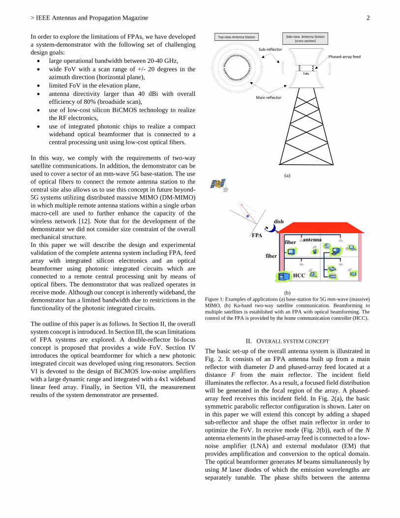
array solutions have major limitations: they are far too expensive and have a very high power consumption due to the low efficiency of state-of-the-art mm-wave integrated circuits [5]-[7]. An alternative to phased-arrays is the focal-plane array (FPA), which is a hybrid solution that combines the best of both worlds: the robustness, low cost and large bandwidth of conventional reflector-based antenna systems and the flexibility and adaptivity of phased-arrays. However, conventional FPA systems [8]-[9] have a limited field-of-view (FoV) and are often used in narrow-band applications. Recent work in [10]-[11] report an improved FoV using a torus reflector at the expense of a relative large main reflector. In the reported torus concept only a small number of array elements in the phased-array feed (PAF) are active simultaneously, which is a major draw-back in our case, since we would like to use silicon-based electronics with a limited output power. This requires a large number of PAF elements to be active at the same time. In this paper we will investigate how these limitations can be overcome. Fig. 1 shows two target applications of FPAs. Base-stations for mm-wave 5G should provide massive-MIMO capabilities and should be able to cover urban macro-cell sizes up to 300 m [2]. This requires a large antenna gain in order to overcome the non-line-of-sight (NLOS) propagation loss, which can be as high as 140 dB. Fig. 1a shows an illustration of such a base-station utilizing the FPA concept, providing high antenna gain and a high effective isotropic radiated power (EIRP). The base-station provides omni-directional coverage in the azimuth (horizontal) direction and limited beam scanning in elevation (+/- 50). Note that the 3600 azimuth coverage could be split in several sections. Another application that is considered is Ka-band two-way satellite communication as illustrated in Fig. 1b. In this case, multiple satellites operating at different frequency bands can be addressed simultaneously. In order to obtain a wide instantaneous bandwidth, we propose to use a novel optical beamforming system that can be controlled by the home communication controller.
2 M. Geurts is with NXP Semiconductors, The Netherlands, [email protected].
Building 5G Millimeter-wave Wireless Infrastructure: Wide-Scan Focal Plane Arrays
with Broadband Optical Beamforming A.B. Smolders1, Senior member IEEE, A. Dubok, Student Member, IEEE, N.M. Tessema, Student
Member, IEEE, Z.Chen, Student Member, IEEE, A. Al-Rawi, Student Member, IEEE, U. Johannsen, Member, IEEE, T. Bressner, Student Member, IEEE, D. Milosovic, Member, IEEE, H. Gao, Member,
IEEE, E. Tangdiongga, Member, IEEE, G. Gerini, , Senior Member, IEEE, P.G.M. Baltus, Senior Member, IEEE, M. Geurts2, A.M.J. Koonen, Fellow IEEE
T
> IEEE Antennas and Propagation Magazine
2
In order to explore the limitations of FPAs, we have developed a system-demonstrator with the following set of challenging design goals: • large operational bandwidth between 20-40 GHz, • wide FoV with a scan range of +/- 20 degrees in the
azimuth direction (horizontal plane), • limited FoV in the elevation plane, • antenna directivity larger than 40 dBi with overall
efficiency of 80% (broadside scan), • use of low-cost silicon BiCMOS technology to realize
the RF electronics, • use of integrated photonic chips to realize a compact
wideband optical beamformer that is connected to a central processing unit using low-cost optical fibers.
In this way, we comply with the requirements of two-way satellite communications. In addition, the demonstrator can be used to cover a sector of an mm-wave 5G base-station. The use of optical fibers to connect the remote antenna station to the central site also allows us to use this concept in future beyond-5G systems utilizing distributed massive MIMO (DM-MIMO) in which multiple remote antenna stations within a single urban macro-cell are used to further enhance the capacity of the wireless network [12]. Note that for the development of the demonstrator we did not consider size constraint of the overall mechanical structure. In this paper we will describe the design and experimental validation of the complete antenna system including FPA, feed array with integrated silicon electronics and an optical beamformer using photonic integrated circuits which are connected to a remote central processing unit by means of optical fibers. The demonstrator that was realized operates in receive mode. Although our concept is inherently wideband, the demonstrator has a limited bandwidth due to restrictions in the functionality of the photonic integrated circuits. The outline of this paper is as follows. In Section II, the overall system concept is introduced. In Section III, the scan limitations of FPA systems are explored. A double-reflector bi-focus concept is proposed that provides a wide FoV. Section IV introduces the optical beamformer for which a new photonic integrated circuit was developed using ring resonators. Section VI is devoted to the design of BiCMOS low-noise amplifiers with a large dynamic range and integrated with a 4x1 wideband linear feed array. Finally, in Section VII, the measurement results of the system demonstrator are presented.
(a)
(b) Figure 1: Examples of applications (a) base-station for 5G mm-wave (massive) MIMO, (b) Ka-band two-way satellite communication. Beamforming to multiple satellites is established with an FPA with optical beamforming. The control of the FPA is provided by the home communication controller (HCC).
II. OVERALL SYSTEM CONCEPT The basic set-up of the overall antenna system is illustrated in Fig. 2. It consists of an FPA antenna built up from a main reflector with diameter D and phased-array feed located at a distance F from the main reflector. The incident field illuminates the reflector. As a result, a focused field distribution will be generated in the focal region of the array. A phased-array feed receives this incident field. In Fig. 2(a), the basic symmetric parabolic reflector configuration is shown. Later on in this paper we will extend this concept by adding a shaped sub-reflector and shape the offset main reflector in order to optimize the FoV. In receive mode (Fig. 2(b)), each of the N antenna elements in the phased-array feed is connected to a low-noise amplifier (LNA) and external modulator (EM) that provides amplification and conversion to the optical domain. The optical beamformer generates M beams simultaneously by using M laser diodes of which the emission wavelengths are separately tunable. The phase shifts between the antenna
Side-view Antenna Station(cross-section)
Top-view Antenna Station
Sub-reflector
Main reflector
Phased-array feed
> IEEE Antennas and Propagation Magazine
3
elements are achieved by optical phase shifters, i.e. micro-ring resonators. The phase shift in a micro-ring resonator depends periodically on the wavelength and on the refractive index of the optical micro-ring waveguide [13].
(a)
(b)
(c) Figure 2: Overall system concept (a) basic form of a single-dish FPA antenna, (b) optical beamforming network in receive mode consisting of N antenna nodes that generate M simultaneous beams, (c) optical beamforming network in transmit mode generating multiple beams by using multiple tunable optical wavelengths. By positioning the wavelength of each tunable laser diode individually on the slope of one of the group delay peaks, a different group delay (and thus phase shift) at each wavelength
can be obtained. This allows the simultaneous reception of M radio beams for which the antenna reception patterns are individually adjustable, by remotely wavelength-tuning the laser diodes in the central site. After wavelength de-multiplexing at the central site, individual amplitude weighing of each of the received wavelength channels is done to provide the optimal conjugate match of the incident field in the focal plane of the FPA [14]. In transmit mode (Fig. 2(c)), multiple beams are generated by using multiple tunable optical wavelengths.
III. BROADBAND WIDE-SCAN FOCAL-PLANE ARRAYS The FoV of a classical parabolic prime-focus FPA (Fig. 2(a)) is very limited. Only a very small number of antenna elements in the phased-array feed are illuminated simultaneously. In [15] it was shown that for a prime-focus FPA with F/D=0.6 only 3.1% of all active array elements are used at the same time for a scan range up to 30 and aperture efficiency of 80% at broadside using an ideal feed. In case of transmitting, this would result in a low EIRP and would exclude the use of low-cost silicon-based RF integrated circuits. For even larger scan-angles the situation becomes even more dramatic. A way to improve this is by using a double-parabolic reflector FPA as shown in Fig. 3. The double-reflector configuration of Fig. 3(a) significantly improves the number of simultaneously active elements as compared to a single-reflector FPA. For a configuration with Fm/Dm=0.6 up to 9.1% of the array elements are active at the same time when scanning up to 30 [15]. However, a major drawback of the double-reflector configuration of Fig. 3(a) is the so-called magnification factor Ma [16], which states that the incident angle seen by the phased-array feed is a factor Ma larger as compared to the incidence angle θ0. As a result, the required number of array elements to support a certain scan range is much larger.
(a) (b) Figure 3: Double-reflector FPAs with (a) symmetrical double-parabolic reflector, (b) optimized ring-focus double reflector. This situation can be improved by optimizing the shape of the sub-reflector. In this way, up to 22.7 % of the array elements are active simultaneously for scan angles up to 30. For a configuration operating at 30 GHz, this would require an array feed size (La) of about 115 mm, assuming a rectangular array with element spacing of λ0/2=5 mm at this frequency. However, our application requires a much larger FoV. This can be
Main reflector
Phased-array feed
F
D
Incident field
La
N 2 1
Fiber 1Fiber 2
Fiber N
Fiber link
Antenna site Central site
λ demux
τg τg
τg τg
Antenna site Central site
N 2 1
Fiber link
RF 1
RF 2
RF M

> IEEE Antennas and Propagation Magazine
4
achieved by using a more complex double-reflector system with a shaped bi-focus sub-reflector as illustrated in Fig. 4. An offset configuration is used to avoid blocking from the relative large reflector. The required array size for scanning up to ±200 with an aperture efficiency of 80% (ideal feed and broadside beam) is now 280 mm at 30 GHz of which 21.4% of the array elements are active simultaneously to create a single beam.
Figure 4: Optimized offset double-reflector FPA with a bi-focus shaped sub-reflector providing a scan range up to 200. The wave trajectory of an incident wave is shown. Key dimensions of optimized configuration are: main reflector size is 80 cm, sub-reflector size is 83 cm by 25.5 cm, focal length of sub-reflector Fs=79 cm and offset between main and sub-reflector zoff=10 cm.
IV. OPTICAL BEAMFORMING USING RING RESONATORS As discussed in section II, an optical beamforming network provides wideband beamforming control of an FPA antenna system with the capability to create multiple beams by using multiple wavelengths for the lasers. The optical beamformer utilizes true time delay (TTD), implemented in a photonic integrated circuit (PIC). The beamforming control is enabled by an optical micro-ring resonator (ORR) which provides a continuously tunable delay via thermos-optic tuning. Thermo-optic tunability in an ORR is enabled via a heater. The schematic structure of a thermally-tunable ORR is shown in Fig. 5 (a). The heaters generate a phase shift on the waveguide due to thermally induced change in the refractive index.
(a)
(b)
Figure 5: Schematic of (a) an Optical Micro ring resonator (ORR) (b) Optical Sideband Filter (OSBF)
The principle of operation involves thermal control of the power coupling ratio κ via a heater within the coupling section which controls the amount of power fed into the feedback loop of an ORR [17]-[18]. Accordingly, the amount of time the input light stays inside the ORR is controlled and hence the generated time delay by the optical beamformer is continuously tuned. The relation of the generated time delay in an ORR with κ is graphically illustrated in Fig. 6. For decreasing values of κ, increased ORR delay is generated. A second heater on the feedback loop of an ORR enables fine tuning of the ORR delay response. Because of the spectral periodicity in an ORR delay response, several unique delay values can be tuned simultaneously with the use of multiple input wavelengths. This allows generating multiple radio beams via multiple wavelengths in a single ORR [19]. The optical beamformer is inherently broadband in the sense that it can enable beamforming for any RF carrier frequency (in this case 20-40 GHz) due to periodic response of the ORR. The delay bandwidth of a single ORR per carrier frequency is limited to 1-3 GHz, but an increased bandwidth in the order of several GHz can be realized by cascading several ORRs within the optical beamformer as demonstrated in [13].
Figure 6: Simulated group delay response (for an ORR with a free spectral range of 0.21 nm (26.5 GHz)), as a function of power coupling ratio κ.
The ORR functionality is supported by an optical sideband filter (OSBF) which converts a double side-band modulated signal into a single side-band signal and band limits the signal. This relaxes the delay bandwidth requirement of an ORR TTD [18]. A typical OSBF implementation is shown in Fig. 5(b). Via the use of thermo-optic tunability of its heating elements, the OSBF can be configured to a desired shape. We realized a four-channel optical beamformer implementation (with four input and four output fibers) based on ORR delay in an integrated circuit. It is fabricated and packaged as shown in Fig. 7. The optical beamforming chip is realized in a Si3N4 integration platform, because of its low-loss and thermo-optic features. The optical chip is transparent only to transverse electromagnetic (TE) polarization. The optical beamformer chip is placed on a PCB for the wire bonding of the DC power-supply contacts pads of the ORR heaters. Embedded arrays of voltage drivers supply a DC voltage for the thermo-optic tuning of the ORRs. The voltage level is controlled on a computer via digital-to-analog (DAC) units. The packaging has a mechanism to
bi-focal sub-reflector
shapedmain reflector
phased-arrayfeed
1549.9 1550 1550.1 1550.2 1550.3 1550.40
50
100
150
200
250
300 delay tuning of an ORR
wavelength (nm)
dela
y (p
s)
κ=0.4κ=0.5κ=0.6κ=0.7κ=0.8κ=0.9κ=1

> IEEE Antennas and Propagation Magazine
5
stabilize the temperature of the optical beamformer chip via a thermo-electric cooling (TEC) controllers. The electro-packaging facilitates system integration of the TTD chip within the optical beamformer system. As a result, the packaged optical beamforming chip is used in the system demonstrator presented in section VI.
Figure 7: Electro-optically packaged TTD chip on the Si3N4 platform for a four-channel radio beamformer (with 4 ORRs)
V. ACTIVE PHASED-ARRAY FEED USING LOW-NOISE AMPLIFIERS WITH A LARGE DYNAMIC RANGE
In this hybrid RF-optical system, the broadband LNA is one of the bottlenecks. The LNA should provide a low noise figure and high gain over a large operational bandwidth to satisfy the sensitivity and dynamic range requirements. A high power gain of at least 25 dB is required, since the LNAs should drive the optical modulators. In addition, the LNA should be realized in a low-cost silicon technology to ensure future integration with other analog and digital electronic circuits. Furthermore, the packaged LNA should fit within the array grid spacing that is required in our FPA concept. Fig. 8(a) shows a photo of the realized phased-array feed, consisting of four wideband bow-tie like antennas [20]-[21] connected to high-gain LNAs which are connected via a rat-race balun to RF cables used to validate the performance of the active 4x1 array. The differential antenna elements are directly matched to the input of the LNA to ensure a low overall noise figure and good power matching. The packaging concept is illustrated in Fig. 8(b)-(c). The silicon LNA chips and bond wires are covered with black glob-top material. To satisfy all requirements aforementioned, various circuit concepts are compared and several design techniques regarding the input matching network are combined. The common-emitter (CE) structure with inductive degeneration and series input inductor is widely used in LNA designs to achieve simultaneous noise and power matching (SNPM) [22-23]. However, the matching condition is only valid at a single frequency if the input matching network only uses one inductor-
capacitor (LC) tank. To achieve broadband SNPM, a dual-LC tank matching method was previously proposed in [25]. Nevertheless, the power gain is low (10.5 dB) and the reverse isolation is limited (25-30 dB). The differential structure circuit provides high reverse isolation and directly feeds to the balanced bow-tie antenna [20]-[21]. However, the input matching network requires at least four inductors to achieve wideband behaviour, which is challenging at mm-wave frequencies considering the layout complexity and mutual coupling among them.
(a)
(b)
(c)
Figure 8: (a) Photo of the 4x1 linear feed array with SiGe BiCMOS LNAs, (b) cross section of the packaging concept where a silicon chip with a thickness of 250 µm is placed in a cavity made in the top PCB layer using Rogers 4003 material, (c) top view of the assembled chip with bond wires on a separate test board. The chip is connected to the top-metal layer of the PCB using bond wires. The silicon chips and bond wires are covered with black glob-top material.
As a result, a 3-winding transformer-based dual-tank matching technique is applied to replace the inductors to achieve a robust and compact solution for wideband applications [26]. The final design of this LNA consists of two stages using differential cascade structures and three stages with multiple-winding transformers as input/inter-stage and output matching
160
R4003 (εr = 3.6)
FR4 (εr = 4.4)
Silicon Chip
150 μm
250 μm 400 μm
800 μm
M1
M2
M2
18 μm (Cu)
RF INPUT
RF OUTPUT

> IEEE Antennas and Propagation Magazine
6
networks. The chip is realized in a silicon-germanium (SiGe) BiCMOS technology and is experimentally validated on a probe station using a fully calibrated four-port vector network analyser setup (for S-parameter measurement) and a two-port spectrum analyser for noise figure and linearity measurements. The results are summarized and compared with other LNAs in Table I. We can conclude that this LNA can support this wireless-optical link by providing a power gain of 28.5 dB and a noise figure of 3.1 dB with an 8 GHz bandwidth. To cover a broader bandwidth, two or more LNAs should be put in parallel.
Table. I: Performance summary and comparison of the BiCMOS LNA chip This
work TMTT
2015 [27] ASSCC
2016 [24] MWCL
2007 [25] Gain (dB) 28.5 26 10.5 23.5
3-dB Gain BW (GHz) 29-37 25-34* 17-43 31-35*
NF (dB) 3.1-4.1 2.1-3.5 2.5-4.0 2.6-3.2 S11<-10dB BW (GHz) 24-40 N/A 17-50 26-40*
IIP3 (dBm)
-12.5 to -7
-5@ 31GHz 1.8 to 5.9 -19.5@
30GHz Power (mW) 80 134 24 11
Technology 0.25 µm SiGe
0.25 µm SiGe
0.25 µm SiGe
0.12 µm SiGe
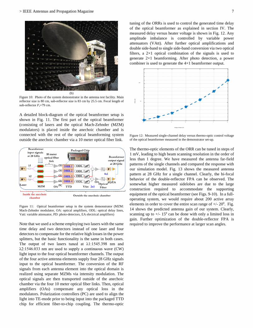
VI. SYSTEM DEMONSTRATOR The overall system demonstrator is shown in Fig. 9 and Fig.10. It operates in receive-mode and consists of the optimized offset double-reflector FPA with the 4x1 active phased-array feed of Fig. 8(a) which is connected to the four-channel optical beamformer. The feed array is positioned in the center of the focal plane. Measurements have been performed in the near-field test facility of Eindhoven University of Technology.
Figure 9: System demonstrator in the near-field scanner antenna test facility. It consists of a wide-scan double-reflector FPA with a 4-element active phased-array feed (see Fig. 8a) connected to the optical beamformer with optical-ring resonators (ORR) and delay lines (ODL). This antenna system is connected to a
remote central processing unit using optical fibers.
Focal-planeArray (FPA)
Optical Modulator
Near-FieldScanner
VNA
> IEEE Antennas and Propagation Magazine
7
(b)
Figure 10: Photo of the system demonstrator in the antenna test facility. Main reflector size is 80 cm, sub-reflector size is 83 cm by 25.5 cm. Focal length of sub-reflector Fs=79 cm. A detailed block-diagram of the optical beamformer setup is shown in Fig. 11. The first part of the optical beamformer (consisting of lasers and the optical Mach-Zehnder (MZM) modulators) is placed inside the anechoic chamber and is connected with the rest of the optical beamforming system outside the anechoic chamber via a 10 meter optical fiber link.
Figure 11: Optical beamformer setup in the system demonstrator (MZM: Mach-Zehnder modulator, OA: optical amplifiers, ODL: optical delay lines, Vatt: variable attenuator, PD: photo-detectors, EA electrical amplifiers) Note that we used a scheme employing two lasers with the same time delay and two detectors instead of one laser and four detectors to compensate for the relative high losses in the power splitters, but the basic functionality is the same in both cases. The output of two lasers tuned at λ1:1545.398 nm and λ2:1546.033 nm are used to supply a continuous wave (CW) light input to the four optical beamformer channels. The output of the four active antenna elements supply four 28 GHz signals input to the optical beamformer. The conversion of the RF signals from each antenna element into the optical domain is realized using separate MZMs via intensity modulation. The optical signals are then transported outside of the anechoic chamber via the four 10 meter optical fiber links. Then, optical amplifiers (OAs) compensate any optical loss in the modulators. Polarization controllers (PC) are used to align the light into TE-mode prior to being input into the packaged TTD chip for efficient fiber-to-chip coupling. The thermo-optic
tuning of the ORRs is used to control the generated time delay of the optical beamformer as explained in section IV. The measured delay versus heater voltage is shown in Fig. 12. Any amplitude imbalance is controlled by variable power attenuators (VAtt). After further optical amplifications and double side-band to single side-band conversion via two optical filters, a 2×1 optical combination of the signals is used to generate 2×1 beamforming. After photo detection, a power combiner is used to generate the 4×1 beamformer output.
Figure 12: Measured single-channel delay versus thermo-optic control voltage of the optical beamformer measured in the demonstrator set-up. The thermo-optic elements of the ORR can be tuned in steps of 1 mV, leading to high beam scanning resolution in the order of less than 1 degree. We have measured the antenna far-field patterns of the single channels and compared the response with our simulation model. Fig. 13 shows the measured antenna pattern at 28 GHz for a single channel. Clearly, the bi-focal behavior of the double-reflector FPA can be observed. The somewhat higher measured sidelobes are due to the large construction required to accommodate the supporting equipment of the optical beamformer (see Figs. 9-10). In a full-operating system, we would require about 200 active array elements in order to cover the entire scan range of +/- 200. Fig. 14 shows the predicted antenna gain of our system. Clearly, scanning up to +/- 150 can be done with only a limited loss in gain. Further optimization of the double-reflector FPA is required to improve the performance at larger scan angles.
2 3 4 5 6 7 8
Voltage of Heater-2(V)
0
50
100
Del
ay (p
s)

> IEEE Antennas and Propagation Magazine
8
Figure 13: Measured far-field antenna pattern of a single-channel of the complete demonstrator system at the output of optical beamformer, frequency is 28.5 GHz.
Figure 14: Predicted directivity of the double-reflector FPA when using a feed-array with 200 active elements.
VII. CONCLUSIONS AND FUTURE RESEARCH DIRECTIONS It is shown that it is possible to use focal-plane-arrays with a high antenna gain for beam-steering with a relative large field-of-view up to +/-200. By using an optical beamformer, a wide-band system for the 20-40 GHz band can be created with a fiber-based interface to a central processing unit. This hybrid antenna system proves to be a very interesting candidate to be used in future 5G and beyond-5G mm-wave base-stations and in two-way satellite communication systems. We have developed integrated circuits for the most critical components in our system, the low-noise amplifier with high gain and the optical beamformer chip using ring-resonators. A system-level demonstrator was developed that operates in receive mode. Experimental results provide a good correlation with the predicted performance.
ACKNOWLEDGEMENTS This work is part of the FREEBEAM project funded by the Dutch technology foundation NWO-TTW.
REFERENCES [1] S. Parkvall, E. Dahlman, A. Furuskär, and M. Frenne. "NR - The new 5G
radio-access technology," IEEE Communications Standards Magazine, 2017.
[2] 3GPP Tech. Rep. 38.913 V14.0.0, “Study on Scenarios and Requirements for Next Generation Access Technologies (Release 14),” Oct. 2016.
[3] D.R. DeBoer,. R.G. Gough, J.D. Bunton, T.J. Cornwell, R.J. Beresford, S. Johnston, I.J. Feain, A.E. Schinckel, C.A. Jackson, M.J. Kesteven, A. Chippendale, G.A. Hampson, J.D. O'Sullivan, S.G. Hay, C.E. Jacka, T.W. Sweetnam, M.C. Storey, L. Ball, B.J. Boyle, "Australian SKA Pathfinder: A High-Dynamic Range Wide-Field of View Survey Telescope," Proceedings of the IEEE , vol.97, no.8, pp.1507-1521, Aug. 2009.
[4] B.B. Adela, P.T.M. van Zeijl, U. Johannsen and A.B. Smolders, “On-chip antenna integration for millimeter-wave single-chip FMCW radar, providing high efficiency and isolation”, IEEE Transactions on Antennas and Propagation, 64(8), 2016.
[5] A. Hajimiri, H. Hashemi, A. Natarajan, X. Guan, A. Komijani, "Integrated Phased Array Systems in Silicon," Proceedings of the IEEE, vol.93, no.9, pp.1637-1655, Sept. 2005.
[6] J.A.J. Essing, D.M.W. Leenaerts and R. Mahmoudi, A 27GHz, 31dBm power amplifier in a 0.25um SiGe:C BICMOS technology. Proceeding of Bipolar/BiCMOS Circuits and Technology Meeting (BCTM), 28 September - 01 October 2014, Coronado, CA, USA (pp. 143-146), 2014.
[7] A.B. Smolders, “Design and construction of a broadband wide-scan angle phased-array antenna with 4096 radiating elements, Phased Array Systems and Technology”, IEEE International Symposium on, pp.87-92, 15-18 Oct 1996.
[8] B. Rohrdantz, T. Jaschke, T. Reuschel, S. Radzijewski, A. Sieganschin and A. F. Jacob, "An Electronically Scannable Reflector Antenna Using a Planar Active Array Feed at Ka-Band," in IEEE Transactions on Microwave Theory and Techniques, vol. 65, no. 5, pp. 1650-1661, May 2017.
[9] M. Ng Mou Kehn, L. Shafai, "Characterization of dense focal plane array feed for parabolic reflectors in achieving closely overlapping or widely separated multiple beams", Radio Sci., Vol. 44(3), 25 June 2009.
[10] C. Cappellin et al., "Novel multi-beam radiometers for accurate ocean surveillance," The 8th European Conference on Antennas and Propagation (EuCAP 2014), The Hague, 2014, pp. 3531-3535
[11] O. A. Iupikov, M. V. Ivashina, N. Skou, C. Cappellin, K. Pontoppidan and C. G. M. van ’t Klooster, "Multibeam Focal Plane Arrays With Digital Beamforming for High Precision Space-Borne Ocean Remote Sensing," in IEEE Transactions on Antennas and Propagation, vol. 66, no. 2, pp. 737-748, Feb. 2018.
[12] R. Rogolin et al., "Scalable synchronization and reciprocity calibration for distributed multiuser MIMO", IEEE Trans. Wireless Commun., vol. 13, no. 4, pp. 1815-1831, Apr. 2014.
[13] M. Burla, D. A. I. Marpaung, L. Zhuang, M. Rezaul Khan, A. Leinse, W. Beeker, M.Hoekman, R.G. Heideman and C.G.H. Roeloffzen, “Multiwavelength-Integrated Optical Beamformer Based on Wavelength Division Multiplexing for 2-D Phased Array Antennas”, Journal of Lightwave Technology, Vol. 32, No. 20, October 15, 2014, pp. 3509-3520
[14] A. Al-Rawi, A. Dubok, S.J. Geluk, M.H.A.J. Herben and A.B. Smolders, "A comparative study on the parabolic and spherical FPA-fed reflector antenna," 2016 10th European Conference on Antennas and Propagation (EuCAP), Davos, 2016, pp. 1-4.
[15] A. Dubok, A. Al-Rawi, N.M. Tessema, E. Tangdiongga, M.H.A.J. Herben, G. Gerini and A.B. Smolders, “Double reflector configuration for optimal exposure of wideband focal plane arrays with optical beamforming”. IEEE Transactions on Antennas and Propagation, 65(8), 2017.
[16] M. Zimmerman, S.W. Lee, B. Houshmand, Y. Rahmat-Samii and R. Acosta, "A Comparison of Reflector Antenna Designs for Wide-Angle Scanning", NASA Technical Memorandum 101459, Presented at the NASA Technology Workshop for Earth Science Geostationary Platforms, September 21-22, 1988, Hampton, Virginia, USA.
[17] X. Han et al., "A tunable optical waveguide ring resonator for microwave photonic filtering," 2013 IEEE International Topical Meeting on Microwave Photonics (MWP), Alexandria, VA, 2013.
[18] W. Bogaerts, P. De Heyn, T. van Vaerenbergh, K. De Vos, S. Kumar Selvaraja, T. Claes, P. Dumon, P. Bienstman, D. Van Thourhout and R. Baets, "Silicon microring resonators," Laser & Photon. Rev., 6: 47–73, 2012.
Azimuth angle (degrees)
Nor
mal
ized
patt
ern
[dB]
Degree
f = 30 GHz
200
150 100 50 00
Azimuth angle (degrees)
Ante
nna
Gai
n [d
Bi]

> IEEE Antennas and Propagation Magazine
9
[19] N.M. Tessema, Z. Cao, J.H.C. van Zantvoort, K.A. Mekonnen, A.M. Trinidad, E. Tangdiongga, A.B. Smolders and A.M.J. Koonen, "K-band RF Multi-Beamformer Using Si3N4 TTD for Home-Satellite Communications," in Optical Fiber Communication Conference, OSA Technical Digest (online) (Optical Society of America), 2017.
[20] A. Dubok, A. Al-Rawi, M.H.A.J. Herben and A.B. Smolders, "Fundamental challenges for wideband antenna elements in focal-plane arrays," 2015 9th European Conference on Antennas and Propagation (EuCAP), Lisbon, 2015.
[21] A. Dubok, A. Al-Rawi, M.H.A.J. Herben, and A.B. Smolders, “Wideband focal plane connected array”, 2016 10th European Conference on Antennas and Propagation, EuCAP 2016, 10-15 April 2015, Davos, Switzerland (pp. 1-5), 2016.
[22] H. Gao, Q. Ma, D.M.W. Leenaerts and R. Mahmoudi, "A 48-61 GHz LNA in 40-nm CMOS with 3.6 dB minimum NF employing a metal slotting method," 2016 IEEE Radio Frequency Integrated Circuits Symposium, San Francisco, California, USA, 2016.
[23] Q. Ma, D. Leenaerts and R. Mahmoudi, "A 30GHz 2dB NF low noise amplifier for Ka-band applications," 2012 IEEE Radio Frequency Integrated Circuits Symposium, Montreal, QC, 2012, pp. 25-28.
[24] Z. Chen, H. Gao, D.M.W. Leenaerts, D. Milosevic and P.G.M. Baltus, "A 16–43 GHz low-noise amplifer with 2.5–4.0 dB noise figure," 2016 IEEE Asian Solid-State Circuits Conference (A-SSCC), Toyama, 2016.
[25] B.W. Min and G.M. Rebeiz, "Ka-Band SiGe HBT Low Noise Amplifier Design for Simultaneous Noise and Input Power Matching," in IEEE Microwave and Wireless Components Letters, vol. 17, no. 12, pp. 891-893, Dec. 2007.
[26] P. Deixler et al., “QUBiC4X: An fT/fmax = 130/140GHz SiGe:C-BiCMOS manufacturing technology with elite passives for emerging microwave applications,” Bipolar/BiCMOS Circuits and Technology, 2004. Proceedings of the 2004 Meeting, pp. 233 – 236, sept. 2004.
[27] Q. Ma, D.M.W. Leenaerts and P.G.M. Baltus, "Silicon-Based True-Time-Delay Phased-Array Front-Ends at Ka-Band," in IEEE Transactions on Microwave Theory and Techniques, vol. 63, no. 9, pp. 2942-2952, Sept. 2015.