
BTI R 45 NM HIGH-K METAL-GATE PROCESS TECHNOLOGYweb.cecs.pdx.edu/~cgshirl/Documents/2008 IRPS...
6
BTI RELIABILITY OF 45 NM HIGH-K + METAL-GATE PROCESS TECHNOLOGY S. Pae, M. Agostinelli, M. Brazier # , R. Chau*, G. Dewey*, T. Ghani # , M. Hattendorf # , J. Hicks, J. Kavalieros*, K. Kuhn # , M. Kuhn, J. Maiz, M. Metz*, K. Mistry # , C. Prasad, S. Ramey, A. Roskowski # , J. Sandford # , C. Thomas # , J. Thomas, C. Wiegand # , and J. Wiedemer # Logic Technology Development Q&R, # PTD, *CR, Intel Corporation, 5200 N.E. Elam Young Pkwy., Hillsboro, OR 97124, USA. 503-613-3683; fax: 971-214-0305; e-mail: [email protected] ABSTRACT In this paper, Bias-temperature instability (BTI) characterization on 45nm high-K + metal-gate (HK+MG) transistors is presented and degradation mechanism is discussed. Transistors with an un- optimized HK film stack in the early development phase exhibited pre-existing traps and large amount of hysteresis that was consistent with literature. The optimized and final HK process demonstrated NMOS and PMOS BTI on HK+MG transistors that are better than that of SiON at matched E-fields and comparable at targeted 30% higher use fields. The final process also showed no hysteresis due to fast traps thereby allowing us to characterize its intrinsic degradation mechanism. On the optimized process, NMOS BTI is attributed primarily to electron trapping in the HK bulk and HK/SiON interfacial layer (IL) regions. PMOS BTI degradation, on the other hand, is mainly interface driven and is found to be very similar to that observed on conventional SiON transistors. [Keywords: BTI, High-K, Metal gate, Transistors, Reliability.] INTRODUCTION Transistor BTI degradation is a key reliability mechanism in HK+MG process technology. In addition to the PMOS NBTI, NMOS PBTI degradation has been observed [1]. Unacceptably high levels of BTI degradation in both NMOS and PMOS are observed on HK with pre-existing defects and of poor quality. Fast charge trapping/de- trapping has also been reported on HK materials which complicates characterization and calls the validity of conventional DC stress into question. BTI reliability degradation has been shown to be modulated by processing and integration changes such as thermal treatments, adding dopants, and nitridation [2-3]. Better charge trapping properties and improved reliability results on transistors fabricated with silicates dielectrics rather than oxide HK has been also reported [4]. In this paper, we identify intrinsic degradation mechanisms through extensive experimental observations and modeling support. Processing conditions were optimized to achieve BTI degradation on HK+MG that is comparable or better than with SiON dielectrics at 15% to 50% higher E-fields for both NMOS and PMOS respectively. The optimized HK film stack used in 45nm HK+MG process also showed negligible hysteresis and transient trapping associated with fast carriers. EXPERIMENTAL RESULTS The 45nm HK+MG transistors studied in this work have a Hafnium based gate dielectric and dual workfunction metal gate electrodes for NMOS and PMOS. The transistor formation involves HK first and MG last process as detailed in [5]. In this flow, HK is deposited using an ALD process and polysilicon is used for the gate patterning. After ILD0 deposition, a polish step exposes poly gates and the dummy poly is removed. Then, workfunction metal electrodes are deposited followed by a gate fill process. The SiO 2 EOT of the HK plus the Interface Layer (IL) that forms between the HK and the silicon is ~1.0nm. Fig. 1 describes the gate stack, with its SiO 2 like interface layer (IL) and the HK dielectric proper. Metal Gate Transition Layer Si High-K Figure 1. TEM of High-K and Metal gate (HK+MG) transistor stack. Fig. 2(a) shows the typical gate leakage behavior of these 45nm HK+MG transistors measured in inversion, compared to the leakages of 65nm Poly/SiON transistors [6]. Substantial reduction (by 25- 1000X) in gate leakage stems from the fact that physically thicker HK film is used while still maintaining a historical inversion Tox scaling trend of ~0.7X per technology generation. Fig. 2(b) shows the appropriate band diagrams for these HK+MG transistors. Lower inversion gate leakage current on the HK+MG PMOS is due to larger band offset than HK+MG NMOS (as indicated by the direction of arrows of the tunneling current). (a) (b) 1E0 -1.2 -0.8 -0.4 0 0.4 0.8 1.2 VGS (V) Normalized Gate Leakage NMOS PMOS SiON 65nm [6] HK+MG 45nm [5] 1E2 1E-2 1E-4 E FM HK IL NWF MG E FM E FSi HK PWF MG NMOS PMOS E FSi Si IL Si E FM HK IL NWF MG E FM E FSi HK PWF MG NMOS PMOS E FSi Si IL Si Figure 2. (a) 45nm HK+MG leakage comparison to that of 65nm Poly/SiON transistors. HK+MG process enables 25-1000X gate leakage reduction. (b) Band diagrams of HK+MG transistors. 352 978-1-4244-2050-6/08/$25.00 ©2008 IEEE IEEE CFP08RPS-CDR 46 th Annual International Reliability Physics Symposium, Phoenix, 2008 Authorized licensed use limited to: PORTLAND STATE UNIVERSITY. Downloaded on March 29, 2009 at 03:19 from IEEE Xplore. Restrictions apply.
Transcript of BTI R 45 NM HIGH-K METAL-GATE PROCESS TECHNOLOGYweb.cecs.pdx.edu/~cgshirl/Documents/2008 IRPS...

BTI RELIABILITY OF 45 NM HIGH-K + METAL-GATE PROCESS TECHNOLOGY
S. Pae, M. Agostinelli, M. Brazier#, R. Chau*, G. Dewey*, T. Ghani#, M. Hattendorf#, J. Hicks, J. Kavalieros*, K. Kuhn#, M. Kuhn, J. Maiz, M. Metz*, K. Mistry#, C. Prasad, S. Ramey, A. Roskowski#, J. Sandford#, C. Thomas#, J. Thomas, C. Wiegand#, and J. Wiedemer# Logic Technology Development Q&R, #PTD, *CR, Intel Corporation, 5200 N.E. Elam Young Pkwy., Hillsboro, OR 97124, USA.
503-613-3683; fax: 971-214-0305; e-mail: [email protected]
ABSTRACT
In this paper, Bias-temperature instability (BTI) characterization on 45nm high-K + metal-gate (HK+MG) transistors is presented and degradation mechanism is discussed. Transistors with an un-optimized HK film stack in the early development phase exhibited pre-existing traps and large amount of hysteresis that was consistent with literature. The optimized and final HK process demonstrated NMOS and PMOS BTI on HK+MG transistors that are better than that of SiON at matched E-fields and comparable at targeted 30% higher use fields. The final process also showed no hysteresis due to fast traps thereby allowing us to characterize its intrinsic degradation mechanism. On the optimized process, NMOS BTI is attributed primarily to electron trapping in the HK bulk and HK/SiON interfacial layer (IL) regions. PMOS BTI degradation, on the other hand, is mainly interface driven and is found to be very similar to that observed on conventional SiON transistors. [Keywords: BTI, High-K, Metal gate, Transistors, Reliability.]
INTRODUCTION
Transistor BTI degradation is a key reliability mechanism in HK+MG process technology. In addition to the PMOS NBTI, NMOS PBTI degradation has been observed [1]. Unacceptably high levels of BTI degradation in both NMOS and PMOS are observed on HK with pre-existing defects and of poor quality. Fast charge trapping/de-trapping has also been reported on HK materials which complicates characterization and calls the validity of conventional DC stress into question. BTI reliability degradation has been shown to be modulated by processing and integration changes such as thermal treatments, adding dopants, and nitridation [2-3]. Better charge trapping properties and improved reliability results on transistors fabricated with silicates dielectrics rather than oxide HK has been also reported [4]. In this paper, we identify intrinsic degradation mechanisms through extensive experimental observations and modeling support. Processing conditions were optimized to achieve BTI degradation on HK+MG that is comparable or better than with SiON dielectrics at 15% to 50% higher E-fields for both NMOS and PMOS respectively. The optimized HK film stack used in 45nm HK+MG process also showed negligible hysteresis and transient trapping associated with fast carriers.
EXPERIMENTAL RESULTS
The 45nm HK+MG transistors studied in this work have a Hafnium based gate dielectric and dual workfunction metal gate electrodes for NMOS and PMOS. The transistor formation involves HK first and MG last process as detailed in [5]. In this flow, HK is deposited using an ALD process and polysilicon is used for the gate patterning. After ILD0 deposition, a polish step exposes poly gates and the dummy poly is removed. Then, workfunction metal electrodes are deposited followed by a gate fill process. The SiO2
EOT of the HK plus the Interface Layer (IL) that forms between the HK and the silicon is ~1.0nm. Fig. 1 describes the gate stack, with its SiO2 like interface layer (IL) and the HK dielectric proper.
Metal Gate
Transition LayerSi
High-K
Metal Gate
Transition LayerSi
High-K
Figure 1. TEM of High-K and Metal gate (HK+MG) transistor stack.
Fig. 2(a) shows the typical gate leakage behavior of these 45nm HK+MG transistors measured in inversion, compared to the leakages of 65nm Poly/SiON transistors [6]. Substantial reduction (by 25-1000X) in gate leakage stems from the fact that physically thicker HK film is used while still maintaining a historical inversion Tox scaling trend of ~0.7X per technology generation. Fig. 2(b) shows the appropriate band diagrams for these HK+MG transistors. Lower inversion gate leakage current on the HK+MG PMOS is due to larger band offset than HK+MG NMOS (as indicated by the direction of arrows of the tunneling current).
(a)
(b)
1E0
-1.2 -0.8 -0.4 0 0.4 0.8 1.2VGS (V)N
orm
aliz
ed G
ate
Leak
age
NMOS PMOS
SiON65nm [4]
HiK+MG45nm
1E2
1E-2
1E-4
1E0
-1.2 -0.8 -0.4 0 0.4 0.8 1.2VGS (V)N
orm
aliz
ed G
ate
Leak
age
NMOS PMOS
SiON65nm [5]
HiK+MG45nm
1E2
1E-2
1E-4
1E0
-1.2 -0.8 -0.4 0 0.4 0.8 1.2VGS (V)N
orm
aliz
ed G
ate
Leak
age
NMOS PMOS
SiON65nm [4]
HiK+MG45nm
1E2
1E-2
1E-4
1E0
-1.2 -0.8 -0.4 0 0.4 0.8 1.2VGS (V)
Nor
mal
ized
Gat
e Le
akag
e
NMOS PMOS
SiON65nm [6]
HK+MG45nm [5]
1E2
1E-2
1E-4
1E0
-1.2 -0.8 -0.4 0 0.4 0.8 1.2VGS (V)N
orm
aliz
ed G
ate
Leak
age
NMOS PMOS
SiON65nm [4]
HiK+MG45nm
1E2
1E-2
1E-4
1E0
-1.2 -0.8 -0.4 0 0.4 0.8 1.2VGS (V)N
orm
aliz
ed G
ate
Leak
age
NMOS PMOS
SiON65nm [5]
HiK+MG45nm
1E2
1E-2
1E-4
1E0
-1.2 -0.8 -0.4 0 0.4 0.8 1.2VGS (V)N
orm
aliz
ed G
ate
Leak
age
NMOS PMOS
SiON65nm [4]
HiK+MG45nm
1E2
1E-2
1E-4
1E0
-1.2 -0.8 -0.4 0 0.4 0.8 1.2VGS (V)
Nor
mal
ized
Gat
e Le
akag
e
NMOS PMOS
SiON65nm [6]
HK+MG45nm [5]
1E2
1E-2
1E-4
EFM
HK IL
NWFMG
EFM
EFSi
HK
PWFMG
NMOS PMOSEFSi
SiIL Si
EFM
HK IL
NWFMG
EFM
EFSi
HK
PWFMG
NMOS PMOSEFSi
SiIL Si
Figure 2. (a) 45nm HK+MG leakage comparison to that of 65nm Poly/SiON transistors. HK+MG process enables 25-1000X gate leakage reduction. (b) Band diagrams of HK+MG transistors.
352978-1-4244-2050-6/08/$25.00 ©2008 IEEE IEEE CFP08RPS-CDR 46th Annual International Reliability
Physics Symposium, Phoenix, 2008
Authorized licensed use limited to: PORTLAND STATE UNIVERSITY. Downloaded on March 29, 2009 at 03:19 from IEEE Xplore. Restrictions apply.
Unless stated otherwise, transistor BTI parameters were evaluated under conventional DC conditions with fixed measurement delay between stress and measurement (SMS). Care was taken such that the measurement phase did not result in additional trap creation. Any recovery due to charge detrapping is kept similar by using the same fixed delay in stress, measurement, and stress cycle. VT was measured using 50mV on the drain. During stress, the gate was biased either with positive or negative polarity while all other terminals were grounded. All of the device results reported for 45nm HK+MG are from the devices that have drawn channel length of 40nm. The actual printed CD was well below 40nm.
The time evolution of 45nm HK+MG NMOS PBTI and PMOS
NBTI is shown in Fig. 3. Both HK+MG NMOS and PMOS BTI degradation over time behavior was similar. NMOS showed slightly lower time slope of 0.17 as compared to PMOS NBTI. PMOS NBTI behavior is very similar to that observed in SiON with power-law time coefficient n of ~0.2 (from the typical NBTI equation of ΔVT ~ tn). The time slope value is not too different than 1/6 (=0.17) reported for H2 diffusion RD model [7] and other reports for HK-based PMOS devices [8]. PMOS with Poly/SiON reference data shown was stressed at different field than HK+MG PMOS and was used to simply illustrate the similarity of the time dependence behavior.
(a) (b)
0.1
1
10
100
1.E+00 1.E+02 1.E+04 1.E+06Stress time (sec)
%ID
sat n ~0.2
HK+MG
SiON+Poly
Stress T=90C
n ~0.17
0.1
1
10
100
1.E+00 1.E+02 1.E+04 1.E+06Stress time (sec)
%ID
sat
Stress T=90C
HK+MG
Figure 3. (a) NMOS PBTI time dependence. (b) PMOS NBTI time dependence of HK+MG transistors. Transistors are drawn at W/L=0.9um/0.04um for HK+MG process. Poly/SiON have W/L=1um/0.04um drawn dimensions.
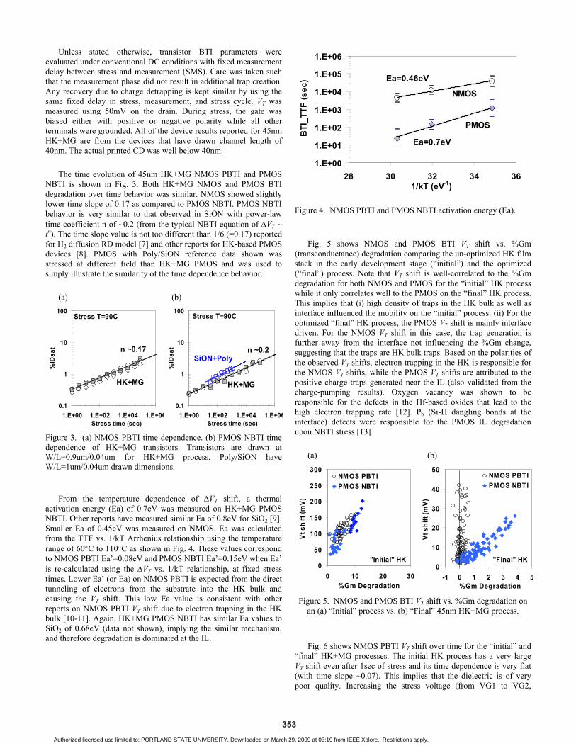
From the temperature dependence of ΔVT shift, a thermal
activation energy (Ea) of 0.7eV was measured on HK+MG PMOS NBTI. Other reports have measured similar Ea of 0.8eV for SiO2 [9]. Smaller Ea of 0.45eV was measured on NMOS. Ea was calculated from the TTF vs. 1/kT Arrhenius relationship using the temperature range of 60°C to 110°C as shown in Fig. 4. These values correspond to NMOS PBTI Ea’=0.08eV and PMOS NBTI Ea’=0.15eV when Ea’ is re-calculated using the ΔVT vs. 1/kT relationship, at fixed stress times. Lower Ea’ (or Ea) on NMOS PBTI is expected from the direct tunneling of electrons from the substrate into the HK bulk and causing the VT shift. This low Ea value is consistent with other reports on NMOS PBTI VT shift due to electron trapping in the HK bulk [10-11]. Again, HK+MG PMOS NBTI has similar Ea values to SiO2 of 0.68eV (data not shown), implying the similar mechanism, and therefore degradation is dominated at the IL.
1.E+00
1.E+01
1.E+02
1.E+03
1.E+04
1.E+05
1.E+06
28 30 32 34 361/kT (eV-1)
BTI
_TTF
(sec
) Ea=0.46eV
Ea=0.7eV
PMOS
NMOS
Figure 4. NMOS PBTI and PMOS NBTI activation energy (Ea).
Fig. 5 shows NMOS and PMOS BTI VT shift vs. %Gm
(transconductance) degradation comparing the un-optimized HK film stack in the early development stage (“initial”) and the optimized (“final”) process. Note that VT shift is well-correlated to the %Gm degradation for both NMOS and PMOS for the “initial” HK process while it only correlates well to the PMOS on the “final” HK process. This implies that (i) high density of traps in the HK bulk as well as interface influenced the mobility on the “initial” process. (ii) For the optimized “final” HK process, the PMOS VT shift is mainly interface driven. For the NMOS VT shift in this case, the trap generation is further away from the interface not influencing the %Gm change, suggesting that the traps are HK bulk traps. Based on the polarities of the observed VT shifts, electron trapping in the HK is responsible for the NMOS VT shifts, while the PMOS VT shifts are attributed to the positive charge traps generated near the IL (also validated from the charge-pumping results). Oxygen vacancy was shown to be responsible for the defects in the Hf-based oxides that lead to the high electron trapping rate [12]. Pb (Si-H dangling bonds at the interface) defects were responsible for the PMOS IL degradation upon NBTI stress [13].
(a) (b)
0
50
100
150
200
250
300
0 10 20 30%Gm Degradation
Vt s
hift
(mV)
NMOS PBTIPMOS NBTI
"Initial" HK0
10
20
30
40
50
-1 0 1 2 3 4 5%Gm Degradation
Vt s
hift
(mV)
NMOS PBTIPMOS NBTI
"Final" HK
Figure 5. NMOS and PMOS BTI VT shift vs. %Gm degradation on
an (a) “Initial” process vs. (b) “Final” 45nm HK+MG process. Fig. 6 shows NMOS PBTI VT shift over time for the “initial” and
“final” HK+MG processes. The initial HK process has a very large VT shift even after 1sec of stress and its time dependence is very flat (with time slope ~0.07). This implies that the dielectric is of very poor quality. Increasing the stress voltage (from VG1 to VG2,
353Authorized licensed use limited to: PORTLAND STATE UNIVERSITY. Downloaded on March 29, 2009 at 03:19 from IEEE Xplore. Restrictions apply.

VG2>VG1, VG2 being much greater) did not change the degradation behavior. Both showed similar flat time dependence. This further confirms that the BTI degradation of this HK dielectric is dominated by very efficient electron filling of high density pre-existing defects/traps. On the other hand, the optimized HK process showed intrinsic BTI behavior similar to that in Fig 3(a) and the observed degradation magnitude depended on the stress voltage, i.e., higher VT degradation was observed with higher gate stress bias. The time dependence is similar for both of the stress conditions on optimized HK process. The reliability differences observed in BTI is also manifested in the gate leakage measurements. Gate leakage is very flat on the “final” HK+MG process, while the “initial” HK+MG process showed early movement and even large increase of leakage current at higher stress biases.
(a) (b)
0
0.5
1
1.5
2
2.5
3
3.5
4
4.5
5
0.1 1 10 100 1000
Stress Time (sec)
IG ra
tio=I
G(t)
to IG
(t=0)
Initial (VG1)Initial (VG2)Final (VG1)Final (VG2)
VG2 > VG1
1
10
100
1000
1 10 100 1000
Stress T ime (sec)
NM
OS
Vt s
hift
(mV)
Initial (VG1)Initial (VG2)Final (VG1)Final (VG2)
VG2 > VG1
Figure 6. (a) NMOS PBTI VT shift and (b) IG characteristics for “initial” and “final” HK+MG process.
Fig. 7 shows results on HK+MG PMOS NBTI supporting similar
conclusions to the HK+MG NMOS BTI discussion above and shown in Fig. 6; except that on PMOS, there’s literally no IG movement. This is again supported by the fact that the traps are mostly interfacial (Dit) and do not distort the field in the dielectric stack at these stress conditions. Again, very high VT shift after only 1sec stress suggests fast trapping mechanism for the initial HK process. These fast trapping was associated with Dit generation and/or hole trapping on the PMOSFET [8, 14]. Initial HK process with higher voltage stress (VG2) showed some sign of IG movement and VT shift was larger.
(a) (b)
00.5
11.5
22.5
33.5
44.5
5
0.1 1 10 100 1000Stress Time (sec)
IG R
atio
= IG
(t) to
IG(t=
0)
Initial (VG1)Initial (VG2)Final (VG1)Final (VG2)
|VG2| > |VG1|
1
10
100
1000
1 10 100 1000Stress T ime (sec)
PMO
S Vt
shi
ft (m
V)
Initial (VG1)Initial (VG2)Final (VG1)Final (VG2)
|VG2| > |VG1|
Figure 7. (a) PMOS NBTI VT shift and (b) IG characteristics for “initial” and “final” HK+MG process.
Based on the above discussions, in summary, the degradation associated with NMOS PBTI is dominated by the bulk HK (the HK/IL interface may also play a role) whereas PMOS NBTI behavior is very similar to SiON, suggesting defect generation close to the interfacial (IL) regions. Further supporting these conclusion are the results of “initial” HK PMOS stressed in accumulation which showed electron trapping behavior similar to HK+MG NMOS PBTI results. Fig. 8 shows PMOS stressed with highly accelerated positive polarity, i.e., PMOS PBTI stress. The results showing an absolute reduction in PMOS VT is consistent with electron trapping in the bulk HK for the “initial” HK process. For the “final” HK process, negligible VT shift was observed even though the stress +Vg was 40% higher and stress times were longer. This further suggested that the HK dielectric was very robust and reliable on the PMOS after all the integrated flows.
-30
-20
-10
0
10
20
30
1 10 100 1000 10000Stress Time (sec)
PMO
S V
t shi
ft (m
V). Final
Initial
Initial HK
Final HK
Figure 8. PMOS PBTI VT shift for “initial” and “final” HK+MG
process. The +Vg used for “final” HK is 40% higher than “initial” HK process. PBTI stress was done at T=125C.
PMOS NBTI in SiO2 exhibits a recovery behavior upon removal
of stress. This recovery behavior has been explained within the frame work of RD model by others where dissociated hydrogen from NBTI stress is back-diffused to the interface [15]. More recently, others have suggested a hole detrapping mechanisms for the NBTI recovery [8, 14]. We’ve examined the recovery behavior of the HK+MG PMOS and compared to the PMOS NBTI of SiON. The recovery behavior was very similar (not shown). Similarities in both degradation and recovery mechanism in HK+MG PMOS to SiON PMOS behavior validates that the NBTI mechanism is related to IL degradation. Recovery on NMOS was also examined and showed smaller recovery rate than the PMOS. More study is needed to understand the NMOS recovery mechanism and differences to the PMOS recovery behavior.
Table I summarizes key intrinsic characteristics of NMOS vs. PMOS BTI mechanisms as discussed.
TABLE 1. COMPARISON OF NMOS AND PMOS BTI RESULTS
NMOS PBTI PMOS NBTI(i) PBTI Vt-shift not correlated to %Gm (i) NBTI Vt-shift vs . %Gm degradation(ii) Vtn increase suggests electon(-) trap (ii) Vtp increase sugges t (+)chg trap(iii) Strong s ignal on HK quality/change (iii) Similar time s lope, Ea vs . SiON
(v) Recovery s imilar to SiON (not shown)
354Authorized licensed use limited to: PORTLAND STATE UNIVERSITY. Downloaded on March 29, 2009 at 03:19 from IEEE Xplore. Restrictions apply.

Fig. 10 shows the BTI characteristic on material with some hysteresis. The change in time dependence with stress can be explained by the presence of fast traps. For simplistic modeling, VT
shift can be expressed as VT=A+B tn, where A=fast trap component, B=true BTI component. Fig. 10b shows that fast traps are not very sensitive to temperature, consistent with [16], and true BTI degradation can be estimated with longer stress on material with non-negligible hysteresis. The fast trap component A is negligible on the final optimized process. In [8], the fast trapping component is described by using logarithmic time dependence. Our fast trapping component can also be fit well with logarithmic time dependence. This fast trapping component is either significantly suppressed or eliminated on a high-quality dielectric [17-18]. Intrinsic degradation (or permanent component of the degradation) can be probed at longer stress times, which is critical for the accurate lifetime assessment [19]. (a) (b)
10
100
1000
1.E+00 1.E+02 1.E+04 1.E+06
stress time (s)
Vt-
shift
(m
V)
ModelBTI comp Trap comp
1
10
100
1 10 100 1000
stress time (s)
Vt-
shift
(m
V)
T=125C
T=100C
T=75C
Figure 10. (a) BTI model with existing traps for “initial” process. (b) Fast trap component shows very weak temperature effect.
0
10
20
30
40
50
5 7 9 11 13SiO2 equivalent EField (MV/cm)
Vt i
ncre
ase
(mV
)
SiON+Poly65nm
45nm HK+MG
PMOS NBTI
Figure 11. PMOS NBTI VT shift vs. Electric field.
0
10
20
30
40
50
5 7 9 11 13SiO2 equivalent EField (MV/cm)
Vt i
ncre
ase
(mV
)
45nm HK+MG
SiON+Poly
NMOS PBTI
Figure 12. NMOS PBTI VT shift vs. Electric field.
Fig. 13a shows 45nm HK+MG Ring Oscillator (RO) stress data with time slope of ~0.2 similar to the device level BTI. Fig. 13b shows the RO stress data vs BTI model based on device level data showing very good agreement.
Fast traps in HK can lead to large instabilities and DC measurements can underestimate the actual degradation in these cases. Fig. 9 shows pulsed IV characteristics for the (a) “initial” HK and (b) “final” HK process. “Initial” HK that showed high BTI degradation in DC stress also exhibited very large hysteresis in pulsed measurements. For the “final” HK process, hysteresis was negligible and unchanged with pulsed bias demonstrating that fast traps have been virtually eliminated with process improvements. Therefore, conventional DC techniques may be used to characterize BTI.
Fig. 11-12 shows HK+MG BTI better than in SiON can be achieved with the “final” HK process. PMOS NBTI is matched at 50% higher E-field (Fig. 11) while NMOS PBTI is matched at 15% higher E-field (Fig. 12). The net NMOS + PMOS BTI shift is matched at 30% higher E-field compared to SiON. E-field is calculated using Vg over inversion Tox for both 65nm and 45nm transistors. For comparison purposes, NMOS PBTI on SiON is stressed at much higher than the normal operating fields. The dramatic improvement in BTI results from a high quality HK film stack coupled with significant reduction in charge fluence during stress (Fig. 2).
355Authorized licensed use limited to: PORTLAND STATE UNIVERSITY. Downloaded on March 29, 2009 at 03:19 from IEEE Xplore. Restrictions apply.

(a)
Ring Oscillator Degradation
y = 0.80x0.23
0.1
1
10
0.01 0.1 1 10 100Stress time (hr)
% F
req
degr
adat
ion
Ring Oscillator Degradation
y = 0.80x0.23
0.1
1
10
0.01 0.1 1 10 100Stress time (hr)
% F
req
degr
adat
ion
(b)
0.0
0.5
1.0
1.5
2.0
2.5
3.0
type #1 type #2 type #3 type #4
%Fr
eq D
egra
datio
n
125C40C
Figure 13. (a) Ring Oscillator degradation. (b) RO stress data against BTI model based on discrete transistors.
Hf-based HK dielectric has low conduction band offset in contact
with silicon substrate. This reduced barrier has potential risk against the hot carrier injection [20]. Fig. 14 shows NMOS hot electron reliability comparison between the 45nm HK+MG and 65nm Poly/SiON transistors [6]. 45nm HK+MG transistors showed huge improvement in lifetime (>7X at same Isub) over 65nm transistors. TTF to impact ionization slope is very similar between the two technologies suggesting that interfacial layer (IL) is playing an important role.
1E+001E+011E+021E+031E+041E+051E+061E+071E+081E+09
1E-03 1E-02 1E-01 1E+00 1E+01Isub (uA/um)
TTF
(sec
)
65nm Poly/SiON
45nm HK-MG
Figure 14. NMOS hot electron performance of 45nm HK+MG and 65nm Poly/SiON transistors.
Fig. 15 shows high temperature AC stressed Ring Oscillator data performed at several different stress voltages. The power-law time dependence slope is higher with higher Vcc indicating hot carrier mechanism is coming into play in addition to the BTI degradation during RO stress. NMOS hot-electron degradation typically shows a time slope of >0.3-0.4. With reduced stress bias (Vg3 still being much greater than the operation and burn-in voltage), only BTI degradation is apparent with a time slope of ~0.2. This suggests that hot carrier degradation is not likely the reliability limiter for the typical inverter type logic circuits based on 45nm HK+MG process.
y = 0.0005x0.4057
y = 0.0008x0.2949
y = 0.0007x0.2329
0.0%
0.1%
1.0%
10.0%
1.E+00 1.E+01 1.E+02 1.E+03 1.E+04 1.E+05stress time (sec)
%Fr
eq D
egra
datio
n
1.8V1.5V1.4V
Vg1Vg2Vg3
Vg1 >Vg2 >Vg3, T=90C
Figure 15. 45nm HK+MG Ring Oscillator stressed in AC at high temperature.
CONCLUSION
Dramatic improvement in the BTI characteristics of 45nm HK+MG transistors has been demonstrated with net BTI comparable to that observed on SiON at a targeted 30% higher operating field. BTI mechanisms for NMOS and PMOS devices on 45nm HK+MG were extensively studied with DC and pulsed current techniques. Bulk trapping in the HK is found to be the dominant mechanism responsible for NMOS PBTI, whereas PMOS NBTI degradation is interface driven. Both HK bulk and well as IL improvements are therefore needed to address reliability of HK+MG CMOS transistors.
REFERENCES
[1] G. Bersuker et al., “Mechanism of Electron Trapping and Characteristics of Traps in HfO2 Gate Stacks,” IEEE Trans. on Device and Materials Rel., vol. 7, no. 1, pp. 138-145, 2007.
[2] M. Houssa et al., “Detrimental Impact of Hydrogen on Negative Bias Temperature Instabilities in HfO2-based pMOSFETs,” in Symp. VLSI Tech. Dig., pp. 212-213, 2004.
[3] G. Wilk et al., “High-k gate dielectrics: Current status and materials properties considerations,” J. Appl. Phys., vol. 89, no. 10, pp. 5243-5275, 2001.
[4] A. Shanware et al., “Characterization and Comparison of the Charge Trapping in HfSiON and HfO2 Gate Dielectrics,” in IEDM Tech. Dig., pp. 939-942, 2003.
356Authorized licensed use limited to: PORTLAND STATE UNIVERSITY. Downloaded on March 29, 2009 at 03:19 from IEEE Xplore. Restrictions apply.

[5] K. Mistry et al., “A 45nm Logic Technology with High-k + Metal Gate Transistors, Strained Silicon, 9 Cu Interconnect Layers, 193nm Dry Patterning, and 100% Pb-free Packaging,” in IEDM Tech. Dig., 2007.
[6] P. Bai et al., “A 65 nm Logic Technology Featuring 35nm Gate Lengths, Enhanced Channel Strain, 8 Cu Interconnect Layers, Low-k ILD, and 0.57um2 SRAM Cell,” in IEDM Tech. Dig.,pp. 657-660, 2004.
[7] A. Krishnan et al., “Negative bias temperature instability mechanism: The role of molecular hydrogen,” Appl. Phys. Lett., vol. 88, 2006.
[8] H. Reisinger et al., “A Comparison of Very Fast to Very Slow Components in Degradation and Recovery Due to NBTI and Bulk Hole Trapping to Existing Physical Models,” IEEE Trans. on Device and Materials Rel., vol. 7, no. 1, pp. 119-129, 2007.
[9] A. Haggag et al., “Realistic Projections of Product Fails from NBTI and TDDB,” in Proc. Int. Reliability Physics Symp., pp. 541-544, 2006.
[10] G. Ribes et al., “Review on High-k Dielectrics Reliability Issues,” IEEE Trans. on Device and Materials Rel., vol. 5, no. 1, pp. 5-19, 2005.
[11] S. Kalpat et al., “BTI Characteristics and Mechanisms of Metal Gated HfO2 Films with Enhanced Interface/Bulk Process Treatments,” IEEE Trans. on Device and Materials Rel., vol. 5, no. 1, pp. 26-35, 2005.
[12] A. Kang et al., “Electron spin resonance observation of trapped electron centers in atomic-layer-deposited hafnium oxide on Si,” Appl. Phys. Lett., vol. 83, no. 16, pp. 3407-3409, 2003.
[13] M. Houssa et el., “Reaction-dispersive proton transport model for negative bias temperature instabilities,” Appl. Phys. Lett., vol. 86, 093506, 2005.
[14] V. Huard et al., “New characterization and modeling approach for NBTI degradation from transistor to product level,” in IEDM Tech. Dig., 2007.
[15] M. Alam et al., “A Critical Examination of the Mechanics of Dynamic NBTI for PMOSFETs,” in IEDM Tech. Dig., pp. 345-348, 2003.
[16] J. Mitard et al., “Large-Scale Time Characterization and Analysis of PBTI in HfO2/Metal Gate Stacks,” in Proc. Int. Reliability Physics Symp., pp. 174-178, 2006.
[17] M. Rafik et al., “Impact of TiN Metal gate on NBTI assessed by interface states and fast transient effect characterization,” in IEDM Tech. Dig., 2007.
[18] T. Grasser et al., “Simultaneous Extraction of Recoverable and Permanent Components Contributing to Bias-Temperature Instability,” in IEDM Tech. Dig., 2007.
[19] C. Schlunder et al., “On the impact of the NBTI recovery phenomenon on lifetime prediction of modern p-MOSFETs,” in Proc. Int. Integrated Reliability Workshop, pp. 1-4, 2006.
[20] H. Park et al., “Decoupling of Cold-Carrier Effects in Hot-Carrier Reliability Assessment of HfO2 Gated nMOSFETs,” IEEE Electron Device Lett., vol. 27, no. 8, pp. 662-664, 2006.
357Authorized licensed use limited to: PORTLAND STATE UNIVERSITY. Downloaded on March 29, 2009 at 03:19 from IEEE Xplore. Restrictions apply.


![del Alamo AVS 2010 v4 · 2013. 4. 16. · InAs HEMTs (V CC GATE DEL = 0.5V) Si NMOSFETs iedm08 10 100 60 Sub Gate Length [nm] iedm08 iedm07 ... (under 2 nm InP etch stop) •4 nm](https://static.fdocuments.us/doc/165x107/60f915d3f99d0b7a93789764/del-alamo-avs-2010-v4-2013-4-16-inas-hemts-v-cc-gate-del-05v-si-nmosfets.jpg)


