B.Satyanarayana, Tata Institute of Fundamental …bsn/OTHER/satyanarayana-hep2010.pdfDetectors aided...
49
B.Satyanarayana, Tata Institute of Fundamental Research, Mumbai
Transcript of B.Satyanarayana, Tata Institute of Fundamental …bsn/OTHER/satyanarayana-hep2010.pdfDetectors aided...

B.Satyanarayana, Tata Institute of Fundamental Research, Mumbai

B.Satyanarayana, Tata Institute of Fundamental Research, Mumbai
Georges Charpak (1924–2010)
The Nobel Prize in Physics 1992 was awarded to
Georges Charpak "for his invention and development
of particle detectors, in particular the multi-wire
proportional chamber".
“The discoveries of the W and Z bosons at CERN, the
charm quark at SLAC and Brookhaven and the top
quark at Fermilab would not have been possible
without this type of detector, and current research in
high energy physics continues to depend on these
devices”.

Detectors aided major discoveries
B.Satyanarayana, TIFR, Mumbai XIX DAE-BRNS High Energy Physics Symposium, LNMIIT, Jaipur December 13-18, 2010 3
Crookes Tubes: Sir William Crookes (1869-75)
Cloud chamber: Charles Thomas Rees Wilson (1894), Nobel Prize in Physics (1927)
Electron: J.J.Thomson (1897) using Crookes Tubes
“Gold foil apparatus”: Hans Geiger & Ernest Marsden (1909)
Proton: E.Rutherford (1911) using “Gold foil apparatus”
Photon: A.Compton (1923)
Neutron: J.Chadwick (1932)
Positron: C.Anderson (1932)
Muon: C.Anderson & S.Neddermeyer (1937)
Neutral Kaon: G.Rochester & C.Butler (1947) using cloud chamber triggered by Geiger counters
Charged Pion: C.Powell (1947) using photographic emulsions carried aloft by balloons
Lambda: (1947)
Neutral Pion: R.Bjorkland (1949)
Bubble chamber : D.Glaser (1952), Nobel Prize in Physics (1960)
Synchrotron: (1952)
Xi minus: R.Armenteros (1952)
Sigma plus: G.Tomasini (1953) using emulsion technique
Sigma minus: W.Fowler (1953)
Antiproton: W.Segrè (1955)
Antineutron: B.Cork (1956)
MOS transistors: Kahng & Atalla (1960), electronic counters
Multi-Wire Proportional Counter: G.Charpak (1968), Nobel Prize in Physics (1992)
Time Projection Chamber: D.R.Nygren (1974)
Charm quark: SLAC & BNL collaborations (1974)
Super Proton Synchrotron: John Adams et al (1976)
Stochastic cooling: Van der Meer, Nobel Prize in Physics (1984)
Large area (20”) PMT: Hamamatsu (1980)
Resistive Plate Chamber: R.Santonico (1981)
W & Z bosons: UA1 and UA2 collaborations (1983)
Micro Strip Gas Chamber: A.Oed (1988)
Top quark: D0 & CDF collaborations (1995)
Gas Electron Multiplier: F.B.Sauli (1996)
Neutrino oscillation: Super-Kamiokande Collaboration (1998)

Tasks of HEP detectors Tracking detector: Direction, sign and momenta of the particles. Often aided by
magnetic field.
Electromagnetic calorimeter: Energy carried by electrons and photons. Signals
proportional to the energy of the incident particles.
Hadronic calorimeter: Energy carried by hadrons (protons, pions and neutrons).
Muon system: Muons are charged particles that penetrate large amounts of matter,
loosing little of their energy. Essentially made of tracking detectors.
Particle identification: Identification of charged and neutral particles. Charged particles
are identified by combining momentum information with Time-Of-Flight, energy loss
dE/dx, Čherenkov or transition radiation.
Displaced vertex: B-, D- or -tagging achieved with high spatial resolution detectors.
RICH detector: Determines the velocity of a charged particle
Transition radiation detector: Uses the γ-dependent threshold of transition radiation in a
stratified material
Time of flight detector: Discriminates between a lighter and a heavier particle of the
same momentum using their time of flight between two detector planes.
Neutrinos: Detected through inferred momentum conservation.
Dark matter: Principle of nuclear recoil by candidate particles (mainly WIMPs)
B.Satyanarayana, TIFR, Mumbai XIX DAE-BRNS High Energy Physics Symposium, LNMIIT, Jaipur December 13-18, 2010 4

Classification of HEP detectors Non-electronic detectors
Emulsions, cloud chamber, bubble chamber
Gaseous detectors
GM, SWPC, MWPC, PMD, drift chamber, TPC, MSGC, GEMs, streamer tube,
spark chamber, PPAC, RPC, CSC (Types: wired, micro-pattern, wire-less)
Scintillation detectors
Organic (crystals, liquids, plastics, extruded), inorganic crystals, gas, glass
Silicon detectors
Strip, pixel, readout integrated
Photo detectors
PMT, PD, APD, VLPC, SiPM
Liquid ionisation detectors
Scintillator, Argon, Xenon
Hybrid detectors
HPD, LArTPC
B.Satyanarayana, TIFR, Mumbai XIX DAE-BRNS High Energy Physics Symposium, LNMIIT, Jaipur December 13-18, 2010 5
On-detector, high-speed, ultra low-noise front-end
ASICs
Novel data acquisition system architectures,
pipelines and data links
High performance flash ADCs, multi-hit TDCs,
DSPs, FPGAs
Field programmable, complex, multi-level,
trigger schemes
Aided by rapid, concurrent
developments in detector readout
technologies

Gas proportional counters
B.Satyanarayana, TIFR, Mumbai XIX DAE-BRNS High Energy Physics Symposium, LNMIIT, Jaipur December 13-18, 2010 6
SWPC
MWPC
KGF counters
UA1 detector

Features of wire chambers
B.Satyanarayana, TIFR, Mumbai XIX DAE-BRNS High Energy Physics Symposium, LNMIIT, Jaipur December 13-18, 2010 7
Advantages Disadvantages
Excellent time resolution Parallax problem
Large active areas, volumes and custom shapes are relatively
easy to buildElaborate electronics and gas systems, expensive
High dynamic range Electrostatic instability limits the stable wire lengths
Excellent energy resolution S/N limited by photon statistics
2/3 dimensional localisation of incident radiation Widths of induced charges define the pad response function
Spatial resolution of few hundred μmWire spacing limits position accuracy, two track resolution to
~2mm
Rate capabilities of a few kHz/mm2 Limited flux capability, accumulation of positive ions restrict
the rate capabilities

Micro Strip Gas Chamber (MSGC)
B.Satyanarayana, TIFR, Mumbai XIX DAE-BRNS High Energy Physics Symposium, LNMIIT, Jaipur December 13-18, 2010
A pattern of thin anodes and
cathode strips on a insulating
substrate with a pitch of a few
hundred μm.
Electric field setup from a drift
electrode above.
Removes positive ions from the
vicinity of avalanches.
High rate capability; two orders of
magnitude higher than MPWC,
~30μm position resolution.
Streamer to gliding discharge
transition damages strips.
Advances in photolithography and
application of silicon foundry
techniques heralded a new era in
the design and fabrication of “Micro-
pattern detectors”
8

New micro pattern era
B.Satyanarayana, TIFR, Mumbai XIX DAE-BRNS High Energy Physics Symposium, LNMIIT, Jaipur December 13-18, 2010 9
Micro-needle chamber
Successfully used to emit
electrons towards the phosphor
screen in high vacuum, for the
purpose of creation of the flat TV
screens.
No observable gas gain due to
fine needles (<<1μm) and small
amplification region.
Micro-dot chamber
Ultimate gaseous pixel device with
anode dotes surrounded by cathode
rings, on 4” Si wafers.
Anode 2 – 20μm, cathodes 20 -
40μm. Anode cathode gap is 75μm.
Very high gains (~106).
Does not discharge up to very high
gains.

Next generation pattern detectors
B.Satyanarayana, TIFR, Mumbai XIX DAE-BRNS High Energy Physics Symposium, LNMIIT, Jaipur December 13-18, 2010 10
Micro-Megas
Very asymmetric parallel plate chamber.
Uses the semi-saturation of the
Townsend coefficient at high fields
(100kV/cm) in several gas mixtures, to
ensure stability in operation with MIPs.
Electrons drifting from the sensitive
volume into the amplification volume with
an avalanche in the thin multiplying gap.
Provides excellent energy resolution.
Compteur a Trous (CAT)
A narrow hole micro-machined in an
insulator metallised on the surface as the
cathode.
Anode is the metal at the bottom of the
hole.
Removing the insulator leaves the
cathode as a micro-mesh placed with a
thin gap above the readout electrode.
Gains of several 104 usually obtained.

Gas Electron Multipliers (GEMs)
B.Satyanarayana, TIFR, Mumbai XIX DAE-BRNS High Energy Physics Symposium, LNMIIT, Jaipur December 13-18, 2010 11
Manufactured using standard printed circuit
wet etching techniques.
Comprise a thin (~50μm) Kapton foil,
double-sided clad with copper and holes are
perforated through.
Two surfaces are maintained at a potential
gradient; providing field for electron
amplification and an avalanche of electrons.
When coupled with a drift electrode above
and a readout electrode below, it acts as a
micro-pattern detector.
Amplification and detection are decoupled,
i.e. readout is at zero potential. This permits
transfer to a second amplification device and
can be coupled to another GEM.

Other micro-pattern detectors
B.Satyanarayana, TIFR, Mumbai XIX DAE-BRNS High Energy Physics Symposium, LNMIIT, Jaipur December 13-18, 2010 12
Many more detectors were developed using the
GEM concept, such as:
Micro-Wire (μDOT in 3-D)
Micro-Pin Array (MIPA)
Micro-Tube
Micro-Well
Micro-Trench
Micro-Groove
Studies have shown that discharges in the
presence of highly ionising particles appear in
all micro-pattern detectors at gains of a few
thousand.
Can obtain higher gains with poorly quenched
gases (lower operating voltage and higher
diffusion)
Lowers charge density
Lowers photon feedback probability
Safe operation of a combination of an MSGC
and a GEM has been demonstrated up to gains
of ~10000s.

Current trends and directions
B.Satyanarayana, TIFR, Mumbai XIX DAE-BRNS High Energy Physics Symposium, LNMIIT, Jaipur December 13-18, 2010 13
Scintillation light imaging A novel application was developed by integrating a MSGC in
a gas proportional scintillation counter (GPSC).
A reflective CsI photocathode was deposited on the micro-
strip plate surface of the MSGC that serves as the VUV photo
sensor for the scintillation light from Xenon GPSC.
Čherenkov ring imaging Very high gains observed with cascade of four GEMs and
using pure ethane as the operating gas.
Mass production of GEMs 3M Microinterconnect Systems Division Reel-to-reel process,
rolls of 16‟x16‟ templates of detachable GEMs in any patterns.
What is a LEM? A large scale GEM (x10) made with ultra-low radioactivity
materials (OFHC copper plated on Teflon).
In-house fabrication using automatic micro-machining.
Modest increase in V yields gain similar to GEM.
Self-supporting, easy to mount in multi-layers.
Extremely resistant to discharges (lower capacitance).
Adequate solution when no spatial info needed.
Copper on PEEK under construction (zero out-gassing).

Birth of the RPC
B.Satyanarayana, TIFR, Mumbai XIX DAE-BRNS High Energy Physics Symposium, LNMIIT, Jaipur December 13-18, 2010
Spark Counters
Planar metal electrodes.
Streamer mode, leading to conducting
plasma filament connecting two
electrodes.
Rapidly growing anode current is the
signal - large and very fast.
Small detector areas, large dead time.
Parallel Plate Avalanche Counters
(PPACs)
Avalanche mode, increased rate
capability, good time resolution.
External amplification.
Pestov Counters
Narrow gap, ultra high fields
(500kV/cm), high pressure (12 bar).
Excellent time resolution, 25ps.
Demands good surface finish of
electrodes.
14
Application driven RPC designs
B.Satyanarayana, TIFR, Mumbai XIX DAE-BRNS High Energy Physics Symposium, LNMIIT, Jaipur December 13-18, 2010 15
Multi gap RPC
Double gap RPC
Micro RPCHybrid RPC
Single gap RPC
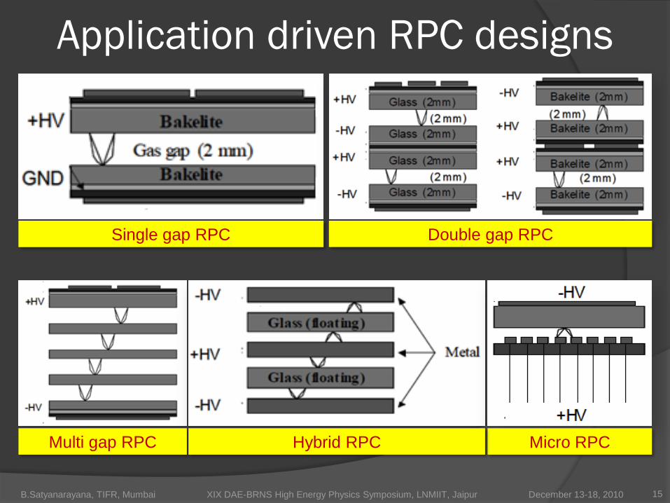
Two modes of RPC operation
B.Satyanarayana, TIFR, Mumbai XIX DAE-BRNS High Energy Physics Symposium, LNMIIT, Jaipur December 13-18, 2010 16
Gain of the detector << 108
Charge developed ~1pC
Needs a preamplifier
Longer life
Typical gas mixture Fr:iB:SF6::94.5:4:0.5
Moderate purity of gases
Higher counting rate capability
Gain of the detector > 108
Charge developed ~ 100pC
No need for a preamplier
Relatively shorter life
Typical gas mixture Fr:iB:Ar::62.8:30
High purity of gases
Low counting rate capability
Avalanche mode Streamer mode

Deployment of RPCs in experiments
B.Satyanarayana, TIFR, Mumbai XIX DAE-BRNS High Energy Physics Symposium, LNMIIT, Jaipur December 13-18, 2010 17
Experiment Area (m2) Electrodes Gap(mm) Gaps Mode Type
PHENIX ? Bakelite 2 2 Avalanche Trigger
NeuLAND 4 Glass 0.6 8 Avalanche Timing
FOPI 6 Glass 0.3 4 Avalanche Timing
HADES 8 Glass 0.3 4 Avalanche Timing
HARP 10 Glass 0.3 4 Avalanche Timing
COVER-PLASTEX 16 Bakelite 2 1 Streamer Timing
EAS-TOP 40 Bakelite 2 1 Streamer Trigger
STAR 50 Glass 0.22 6 Avalanche Timing
CBM TOF 120 Glass 0.25 10 Avalanche Timing
ALICE Muon 140 Bakelite 2 1 Streamer Trigger
ALICE TOF 150 Glass 0.25 10 Avalanche Timing
L3 300 Bakelite 2 2 Streamer Trigger
BESIII 1200 Bakelite 2 1 Streamer Trigger
BaBar 2000 Bakelite 2 1 Streamer Trigger
Belle 2200 Glass 2 2 Streamer Trigger
CMS 2953 Bakelite 2 2 Avalanche Trigger
OPERA 3200 Bakelite 2 1 Streamer Trigger
YBJ-ARGO 5630 Bakelite 2 1 Streamer Trigger
ATLAS 6550 Bakelite 2 1 Avalanche Trigger
ICAL 97,505 Both 2 1 Both Trigger

Performance of RPC systems
B.Satyanarayana, TIFR, Mumbai XIX DAE-BRNS High Energy Physics Symposium, LNMIIT, Jaipur December 13-18, 2010 18
Argo Alice CMS

Picking up the tiny charges
B.Satyanarayana, TIFR, Mumbai XIX DAE-BRNS High Energy Physics Symposium, LNMIIT, Jaipur December 13-18, 2010 19
Process: AMSc35b4c3 (0.35um CMOS)
Input dynamic range:18fC – 1.36pC
Input impedance: 45Ω @350MHz
Amplifier gain: 8mV/μA
3-dB Bandwidth: 274MHz
Rise time: 1.2ns
Comparator‟s sensitivity: 2mV
LVDS drive: 4mA
Power per channel: < 20mW
Package: CLCC48(48-pin)
Chip area: 13mm2
Anusparsh
Manas
NINO

Timing the timing devices
B.Satyanarayana, TIFR, Mumbai XIX DAE-BRNS High Energy Physics Symposium, LNMIIT, Jaipur December 13-18, 2010 20
Jo
rge
n C
hri
sti
an
se
n
FPGA based TDC architecture
960 TDC channels on a board!

Latest designs and developments
B.Satyanarayana, TIFR, Mumbai XIX DAE-BRNS High Energy Physics Symposium, LNMIIT, Jaipur December 13-18, 2010 21
New mixtures containing Helium
Ideally, operating RPC at ½ Atm would reduce the
the operating voltage by a factor of 2.
Helium undergoes elastic scattering with electrons
Takes part only partially in the avalanche
processes
In first approximation behaves like a space holder
Reduces the partial pressure of the active mixture
Effect similar to operating at a reduced pressure
M. Petris José Repond
M. Abbrescia
NeuLAND

Large scale deployment of scintillators
B.Satyanarayana, TIFR, Mumbai XIX DAE-BRNS High Energy Physics Symposium, LNMIIT, Jaipur December 13-18, 2010 22
DZERO
CMS
GRAPES Scintillator tiles with WLS fibre readout

Fermilab and Northern Illinois Center for Accelerator and Detector
Development.
For ALICE upgrade, the ILC calorimetry program, MINOS and MINERA
experiments.
Simple, inexpensive and robust extrusion procedure.
Co-extruded hole and TiO2 coating or Tyvek.
In some cases no alternative to the extrusion because of geometry
requirements.
Polystyrene pellets are used as the base material, along with % PPO (2.5-
Diphenyloxazole) and 0.03% POPOP (1,4-bis(5-phenyloxazol-2-yl)
benzene) dopants.
This is a blue-emitting scintillator, absorption cut-off at 400nm and emission
at 420nm.
Light Attenuation Lengths of long and short components are 42cm & 30cm.
Fiber hole diameter and number of fibres are some of the considerations.
Readout by Solid State Photomultipliers (SSPM).
New development: Co-extrude fibres with the scintillator profile.
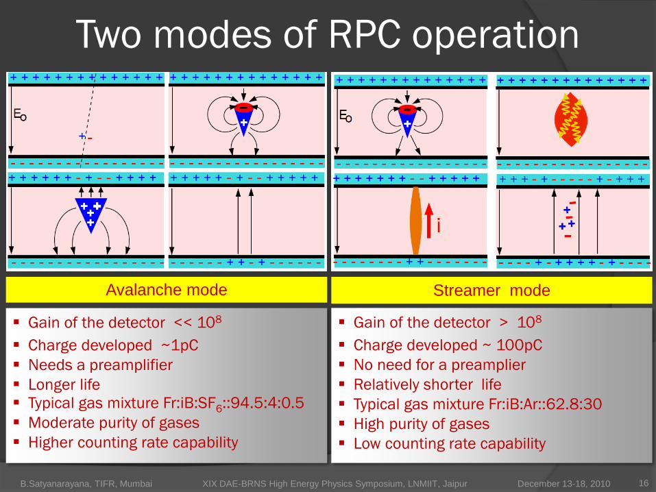
FNAL-NICADD extrusion Line
B.Satyanarayana, TIFR, Mumbai XIX DAE-BRNS High Energy Physics Symposium, LNMIIT, Jaipur December 13-18, 2010 23
Extrusion scintillator technology
B.Satyanarayana, TIFR, Mumbai XIX DAE-BRNS High Energy Physics Symposium, LNMIIT, Jaipur December 13-18, 2010 24

New hybrid scintillators New generation experiments require large volume, cheap scintillation
materials with high light yields and short scintillation decay times.
Extruded scintillators suffer from poorer optical quality, particulate
matter and additives in polystyrene pellets.
New single-component and multi-component polymer mixtures.
Hybrid scintillators using luminescent salts as scintillation dyes.
Introduction of fusible inorganic fillers found to alter optical
transmission spectra and rapid shortening of the scintillation decay
times of the hybrid scintillators.
Polymer based hybrid glasses in which the components do not
chemically react with each other during the manufacturing process.
Conventional hybrid materials in which all or a part of the inorganic
components participate in chemical reactions with organic
components. For example, a reaction between the AlCl3 inorganic filler
and the polystyrene matrix during the injection moulding process.
B.Satyanarayana, TIFR, Mumbai XIX DAE-BRNS High Energy Physics Symposium, LNMIIT, Jaipur December 13-18, 2010 25

In 1979, Masatoshi Koshiba came up with a
challenging proposal to Hamamatsu„s President
Hiruma "Hey, could you make me a 25” PMT?“
A number of previously acquired highly
sophisticated technologies were collectively used
to develop the 20” PMT.
50Kt water Čherenkov detector uses 11.2K PMTs.
R1449 PMTs & neutrino astronomy
B.Satyanarayana, TIFR, Mumbai XIX DAE-BRNS High Energy Physics Symposium, LNMIIT, Jaipur December 13-18, 2010 26
Ham
am
ats
u
Kam
iokande d
ete
cto
r

GM APDs and SiPMs Very small (few mm)
Pixelated active surface structure
Insensitive to magnetic fields
Works at low bias voltage (<100V)
Relatively inexpensive
Single photon counting capability
Very fast time resolution (200ps)
Good linear response
B.Satyanarayana, TIFR, Mumbai XIX DAE-BRNS High Energy Physics Symposium, LNMIIT, Jaipur December 13-18, 2010 27
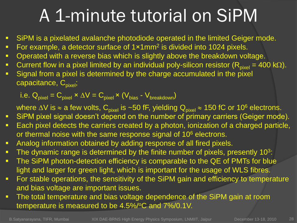
A 1-minute tutorial on SiPM
B.Satyanarayana, TIFR, Mumbai XIX DAE-BRNS High Energy Physics Symposium, LNMIIT, Jaipur December 13-18, 2010 28
SiPM is a pixelated avalanche photodiode operated in the limited Geiger mode.
For example, a detector surface of 1×1mm2 is divided into 1024 pixels.
Operated with a reverse bias which is slightly above the breakdown voltage.
Current flow in a pixel limited by an individual poly-silicon resistor (Rpixel = 400 k).
Signal from a pixel is determined by the charge accumulated in the pixel
capacitance, Cpixel;
i.e. Qpixel = Cpixel × V = Cpixel × (Vbias - Vbreakdown)
where V is a few volts, Cpixel is ~50 fF, yielding Qpixel 150 fC or 106 electrons.
SiPM pixel signal doesn‟t depend on the number of primary carriers (Geiger mode).
Each pixel detects the carriers created by a photon, ionization of a charged particle,
or thermal noise with the same response signal of 106 electrons.
Analog information obtained by adding response of all fired pixels.
The dynamic range is determined by the finite number of pixels, presently 103:
The SiPM photon-detection efficiency is comparable to the QE of PMTs for blue
light and larger for green light, which is important for the usage of WLS fibres.
For stable operations, the sensitivity of the SiPM gain and efficiency to temperature
and bias voltage are important issues.
The total temperature and bias voltage dependence of the SiPM gain at room
temperature is measured to be 4.5%/oC and 7%/0.1V.

Some of the basic characteristics
B.Satyanarayana, TIFR, Mumbai XIX DAE-BRNS High Energy Physics Symposium, LNMIIT, Jaipur December 13-18, 2010 29

Silicon detectors
B.Satyanarayana, TIFR, Mumbai XIX DAE-BRNS High Energy Physics Symposium, LNMIIT, Jaipur December 13-18, 2010 30
Essentially diode with reverse bias.
Depleted of free charge carriers.
High resistance, only small leakage current.
Charge deposition by ionising particle causes
current.
Use segmented electrodes (strips or pixels).
Can localise charge deposition.
Much better resolution than strip pitch if taking
charge sharing into account.
Only few eV per ionisation (gases: factor 10
more).
Good amplitude signal.
Silicon detectors are transforming the way we look at particles

Strip detectors
B.Satyanarayana, TIFR, Mumbai XIX DAE-BRNS High Energy Physics Symposium, LNMIIT, Jaipur December 13-18, 2010 31
Reading out strips is comparatively
easy - just attach chips to the end.
Readout of strip sensor, power
distribution and control → hybrids.
Custom readout chips wire bonded
to electrodes on the sensor.
Chips have amplifiers, ADCs, zero
suppression, cluster finder,
storage, digital communication with
outside world.
Some drawbacks:
Strip detectors would often exceed
useful occupancy in many modern
systems.
Strip information can make hit
reconstruction ambiguous.

Pixel detectors
B.Satyanarayana, TIFR, Mumbai XIX DAE-BRNS High Energy Physics Symposium, LNMIIT, Jaipur December 13-18, 2010 32
Silicon pixel detectors do
much better on the hit
reconstruction problems.
However, reading pixel
detectors is non-trivial.
Options for pixel detector
readout:
Place readout chips all
over the sensors (more
material budget).
Integrate readout
electronics into sensor
(larger pixels).
Sequentially clock signals
through to end of sensor
(slower readout).CMS pixel tracker

Integration of detectors & readout Compatible integration of detectors and readout electronics on the same silicon substrate
is of growing interest.
As the methods of microelectronics technology have already been adapted for detector
fabrication, a common technology basis for detectors and readout electronics is available.
CMOS technology exhibits most attractive features for the compatible realisation of
readout electronics where advanced LSI processing steps are combined with detector
requirements.
The essential requirements for compatible integration are the:
availability of high resistivity oriented single crystalline silicon substrate
formation of suitably doped areas for MOS circuits
isolation of the low voltage circuits from the detector, which is operated at much higher
supply voltage.
Junction isolation as a first approach based on present production technology and
dielectric isolation based on an advanced SOI-LSI technology are the most promising
solutions for present and future applications, respectively.
Some examples: MAPS (Monolithic Active Pixels), DEPFET, WIPS, SOI sensors.
B.Satyanarayana, TIFR, Mumbai XIX DAE-BRNS High Energy Physics Symposium, LNMIIT, Jaipur December 13-18, 2010 33

Integrated silicon detectors
B.Satyanarayana, TIFR, Mumbai XIX DAE-BRNS High Energy Physics Symposium, LNMIIT, Jaipur December 13-18, 2010 34
DEPFET was developed for X-ray applications
Consists of high-resistivity silicon substrate fully depleted through an n+
contact at the side of the sensor.
The first amplifying transistors are integrated directly into the substrate and
form the pixel structure.
Electrons from ionizing particles are collected in this internal gate and modify
the transistor current yielding a signal.
A matrix containing 64 × 64 square pixels of 50 μm size achieved a resolution
of 9.5 μm and 40 e- noise.
MAPS integrate sensors and readout electronics on the same substrate using a
technology similar to the one used in visible light CMOS cameras.
Norb
ert
Werm
es

Challenges facing Si detectors
Main issue is radiation damage.
Silicon detectors are invariably located in the high
dose region (mostly used in trackers).
Surface damage: charge build-up, noise
Bulk damage: displacements in crystal lattice
reduced charge collection efficiency (charge lost in traps).
changes dopant levels and distribution (affects bias
voltage).
increased leakage current (noise).
increase in the voltage required for full depletion.
increase in capacitance between the detecting elements.
B.Satyanarayana, TIFR, Mumbai XIX DAE-BRNS High Energy Physics Symposium, LNMIIT, Jaipur December 13-18, 2010 35

DZERO LAr calorimeter
B.Satyanarayana, TIFR, Mumbai XIX DAE-BRNS High Energy Physics Symposium, LNMIIT, Jaipur December 13-18, 2010 36

Readout of ATLAS LAr calorimeter
B.Satyanarayana, TIFR, Mumbai XIX DAE-BRNS High Energy Physics Symposium, LNMIIT, Jaipur December 13-18, 2010 37
Total:182468 LAr channels

Principle of LArTPC
B.Satyanarayana, TIFR, Mumbai XIX DAE-BRNS High Energy Physics Symposium, LNMIIT, Jaipur December 13-18, 2010 38

600t LAr TPC for ICARUS
B.Satyanarayana, TIFR, Mumbai XIX DAE-BRNS High Energy Physics Symposium, LNMIIT, Jaipur December 13-18, 2010 39
Number of independent containers = 2
Single container internal dimensions: L = 19.6 m, W = 3.9 m, H = 4.2 m
Total (cold) internal volume = 534 m3
Sensitive LAr mass = 600 ton

Methods of TPC readout Single-phase devices do not show any internal gain and therefore rely
on small signal-to-noise ratios and extremely sensitive front-end
electronics.
Double-phase readout, benefits from internal gain due to readout in the
gas-phase where avalanches in argon can increase the primary signal
substantially. The price for this advantage is the restriction to one-
sided, gas readout which enforces either unprecedented long drift
lengths or very large surface area (shallow tank). In addition this
technique battles with space-charge effects at the gas–liquid interface
and necessary tight control of the liquid level, temperature, etc.
Third alternative is liquid argon readout technology. It combines the
separate advantages of both, single-phase operation for the wire
readout and an amplified signal in a double-phase readout. The idea is
to stick to the robust and mature single-phase TPC concept and
implement an optical readout of light produced by electroluminescence
in liquid argon.
B.Satyanarayana, TIFR, Mumbai XIX DAE-BRNS High Energy Physics Symposium, LNMIIT, Jaipur December 13-18, 2010 40

Current work on LAr TPC detectors Liquid Argon Time Projection Chambers (LArTPC) technology is now proven for up to
600t mass. A detector capable of delivering the neutrino physics program of the future
will however need to be on a grander scale still with a fiducial volume of perhaps up to
100 kt.
MODULAr essentially stacks together many ICARUS modules to achieve the final
volume.
GLACIER drifts charge up to 20m through a single huge liquid Argon volume to be
amplified and readout in the gas directly above the liquid volume.
FLARE and LANNDD are also based on a single volume of liquid Argon but which are
internally segmented to limit the maximum charge drift distance and read signals using
wire planes, similar to ICARUS.
The latest project founded on the basis of a LArTPC detector using wire-plane readout
is the ArgoNeuT project, currently taking data in the FNAL neutrino beam.
Targeted experiments of this detector technology:
LAGUNA proton decay and neutrino physics project
RD51 initiative
Upgrades to the T2K experiment
Proposed neutrino factory project
ArDM dark matter experiment
B.Satyanarayana, TIFR, Mumbai XIX DAE-BRNS High Energy Physics Symposium, LNMIIT, Jaipur December 13-18, 2010 41

THGEM readout for TPC
The new concept of operating a Thick Gas Electron Multiplier
(THGEM) directly in the liquid opens the exciting possibility of
fine grained tracking (spatial resolution of order mm) with high
signal to noise ratio using only low-cost, robust components.
Utilising electroluminescence, i.e. light emitted in the THGEM
holes, for optical readout, for instance with silicon
photomultipliers (SiPM), directly in the liquid volume would be
the key new effect in this technology.
The THGEM provides an excellent imaging plane for
electroluminescence.
Electrons initially released by ionisation drift towards the holes,
mechanically drilled through the printed-circuit board, where the
presence of strong electric fields inside the holes results in a grid
of well-localised light sources.
B.Satyanarayana, TIFR, Mumbai XIX DAE-BRNS High Energy Physics Symposium, LNMIIT, Jaipur December 13-18, 2010 42

Optical readout for LAr detectors
B.Satyanarayana, TIFR, Mumbai XIX DAE-BRNS High Energy Physics Symposium, LNMIIT, Jaipur December 13-18, 2010 43
ICARUS has shown that Liquid Argon
is a suitable medium for TPCs for: Calorimetry
Fine Grain tracking
Design of readout planes must keep
electronics cost reasonable.
Optical readout is feasible alternative
to the wire based readout for Liquid
Argon TPC of the future.
Liquid Argon TPC with Thick Gas
Electron Multiplier (THGEM) and
optical readout using Silicon
Photomultipliers (SiPM).

Light readout concept for tracking
B.Satyanarayana, TIFR, Mumbai XIX DAE-BRNS High Energy Physics Symposium, LNMIIT, Jaipur December 13-18, 2010 44
The electroluminescence from the THGEM holes can be imaged by an
optical readout device.
Silicon Photomultipliers (SiPMs) from SENSL were used in this study.
Strong signal output, gain 106.
Arranging sensors in a sparse array above the THGEM allows fewer
readout channels than holes, with no reduction in resolution.
Row and column readout gives 2N readout channels rather than N2.

Proof of principle
B.Satyanarayana, TIFR, Mumbai XIX DAE-BRNS High Energy Physics Symposium, LNMIIT, Jaipur December 13-18, 2010 45

Summary and outlook No detector technology is ready to give up its share or future stack, even as new
players are joining the ring; detectors and electronics dictating each other‟s agenda.
Innovative designs of GEMs, massive research and industrial projects, hybrid designs
with micro-pattern and liquid argon TPCs.
Novel structures and new applications of MRPCs, work in progress in the areas signal
readout and gas systems, 100,000 m2 of single gap RPCs at INO‟s ICAL!
Radiation hard silicon detectors, search for new materials, detectors with larger band
gap, integrated devices.
CVD diamond detectors showing a lot of promise, though not covered in this talk.
Liquid reinventing itself as future detecting medium both at accelerator and non-
accelerator physics experiments for a variety of detecting tasks.
ASICs, FPGAs, high speed data links are no more buzz words, but are basic needs.
Switchable power schemes to the front-end and signal processing electronics.
Industries and applied research units are increasingly being added to the scientific
collaborations‟ list!
And finally, high energy physics experiments are increasingly inheriting
modus operandi of huge international level infrastructure projects – funding,
planning, management, inventions, technology development, costing ,
manufacturing, QA/QC, heterogeneous skills, personnel and even more …
B.Satyanarayana, TIFR, Mumbai XIX DAE-BRNS High Energy Physics Symposium, LNMIIT, Jaipur December 13-18, 2010 46

ThanksTo the organisers for giving me this wonderful opportunity. I feel honoured.To all the researchers whose work I have used freely in this talk.To you for your attention.
B.Satyanarayana, TIFR, Mumbai XIX DAE-BRNS High Energy Physics Symposium, LNMIIT, Jaipur December 13-18, 2010 47

Photon Multiplicity Detector (PMD)
B.Satyanarayana, TIFR, Mumbai XIX DAE-BRNS High Energy Physics Symposium, LNMIIT, Jaipur December 13-18, 2010 48
PMD a pre-shower detector measuring spatial
distribution of photons in the forward rapidity
region.
Complements the study of photons in the
forward region where calorimeter cannot be
used due to high particle density.
Honeycomb (rectangular) proportional counter,
the cells of which are 5 mm deep with a
surface of about 1cm2 (0.22cm2) in
START(ALICE) design.
Confines charged particle hits to single cell.
Copper walls separate the cells in order to
prevent signals from blowing up by confining
low-energy electrons to a single cell.
In the assembled version, the PCBs form part
of a gas-tight chamber having a high voltage
connection and inlet/outlet for the gas.
Readout by GASSIPLEX (Manas) chips in
STAR (ALICE) design.

LAr TPC readout by large area PMT
B.Satyanarayana, TIFR, Mumbai XIX DAE-BRNS High Energy Physics Symposium, LNMIIT, Jaipur December 13-18, 2010 49
Electron Tubes 9357FLA8” PMT (bialkali with Pt deposit)
G = 1 x 10⁷ @ ~1400 V
peak Q.E. (400-420 nm) ~ 18 % (≈10% cold)
Trise ~ 5 ns, FWHM ~ 8 ns
•Commercial PMT with large area
Glass-window
•Scintillation VUV l = 128 nm
Wavelength-shifter (TPB)
•Immersed T(LAr) = 87 K