
Broad Argon Beam for Post FIB Clean-Up -...
34
CONFIDENTIAL (presentation title here) Broad Argon Beam for Post FIB Clean-Up Mike Hassel Shearer 1 & Vikstram Hakan 2 1 Gatan Inc. 2 Oxford Instruments
Transcript of Broad Argon Beam for Post FIB Clean-Up -...

CONFIDENTIAL (presentation title here)
Broad Argon Beam for Post FIB Clean-Up
Mike Hassel Shearer1 & Vikstram Hakan2
1 Gatan Inc. 2 Oxford Instruments

CONFIDENTIAL (presentation title here)
Broad Argon Beam Tools Gatan
JEOL
Technoorg Linda
Fischione
Leica

CONFIDENTIAL (presentation title here)
Sample Preparation and EM
FIB + 300 V Argon Polish
Argon Polish 8Kev + 1 KeV
Argon Polish 6 KeV
Titan TEM Image of Gate + EELS Data later in presentation
SEM Image FOV 500 micron in diameter ready for EBSD
SEM Image FOV 1mm x 600 microns voids as small as 4nm visible . Key analysis in Fracking

CONFIDENTIAL (presentation title here)
Some of the Tools Used for Sample Prep.

CONFIDENTIAL (presentation title here)
Or Even These $$$$$ ! Useful ? Not Always

CONFIDENTIAL (presentation title here) 6
Ion Beam Sample Preparation Broad Ion Beam milling
Suitable for all types of sample materials o Semiconductors, Ceramics, Metals and Geological materials
Requires mechanical pre-preparation of samples o Dimpling technique
o Wedge technique (Tri-Pod / T-Tool) Semiconductors only
Focused ion beam (FIB) technique Expensive, but advantage is precision
Suited primarily to semiconductors for precision cross sections
Can produce considerable ion beam damage (Amorphization layer)
Samples generally not suitable for HREM without additional cleanup
Broad Ion Beam milling + FIB Best of Both Worlds
o Positional Precision of FIB
o Minimal Damage from low energy (~100-300Volt) Argon

CONFIDENTIAL (presentation title here) 7
Factors Influencing Ion Milling
Sputtering rate and artifact formation play a role in ion milling
specimens
Sputtering is the removal of atoms from the surface of a sample by
incident energetic particles.
Sputtering occurs by momentum transfer from energetic particles to
specimen atoms.
Sputtering rates depend on several factors:
Flux and velocity of the incident particles (Gun voltage)
Angle of incidence
Relative masses of the specimen atoms and incident particles.
Cohesive energy of the specimen atoms
Chemical interactions between incident particles and the specimen

CONFIDENTIAL (presentation title here)
Sputtering Yield Calculated average sputtering in atoms per ion
Yield decreases with energy
A maximum occurs between 45 and 10 degree beam angle
8
0
2
4
6
8
10
12
14
0.0 1.0 2.0 3.0 4.0 5.0 6.0 7.0
Sp
utt
erin
g Y
ield
[at
om
s/io
n]
Ion Energy [keV]
Sputtering Yield of Si for various angles (Ar)
90
45
10
8
6
4
2
0
2
4
6
8
10
12
14
16
18
0.0 1.0 2.0 3.0 4.0 5.0 6.0 7.0
Sp
utt
erin
g Y
ield
[ato
ms/
ion
]
Ion Energy [keV]
Sputtering Yield of Si at 4 degree beam angle
Neon
Argon
Xenon
Yield increases with ion mass, so highest for Xenon

CONFIDENTIAL (presentation title here) 9
Factors Influencing Sample Outcome
Instrument related factors
Ion beam voltage --> Low voltage milling is new direction (100eV – 1.0keV)
Ion beam current --> Output of the ion gun affects Sputter rate
Milling angle (Typically 1° – 10°)
o Low angle milling (< 3°) improves sample quality
o Increases milling times
Specimen holder
o Poor design can restrict low angle milling.
o Poor design can add to re-deposition
o Poor design can damage fragile specimens
Sample related factors
Type of sample (Micro-structural features, Heat sensitive materials)
Method of pre-preparation (Electro-polished, Dimpled)
Starting surface must be free of Mechanical damage (Scratches)
Starting thickness (Low angle milling requires thin samples < 70 µm)
Sample mounting

CONFIDENTIAL (presentation title here) 10
FIB Technique
Primary vendors of Focused Ion Beam instruments
FEI, Hitachi, JEOL, TESCAN, Zeiss
Two basic model types
Single beam and dual beam
o Single beam permits milling or viewing
o Dual beam permits simultaneous milling and viewing
Liquid Gallium metal source
<5nm resolution
Beam energies from 1keV to 50keV
Beam currents from 1pA to 10,000pA
Image with either Secondary Electrons (SED) or Secondary Ions

CONFIDENTIAL (presentation title here) 11
FIB Technique
Advantages
Precise cutting of site specific areas
In-situ milling/sectioning and imaging
Precision deposition of metal layers
Disadvantages
High initial cost
Considerable Gallium induced surface damage (20-60nm)
Requires high operator skill
Relatively slow processing compared to standard ion milling

CONFIDENTIAL (presentation title here) 12
Ion Milling Artifacts
Amorphization Layer Formation
Sufficient atom displacement within the collision cascade to lose long-range order
Surface Oxidation / Contamination
On cleaved Si surface in air, always 1.0 – 1.5 nm of amorphous SiO2 present (J.P. McCaffrey et al., Ultramicroscopy 87 (2001), 97-104)
Re-deposition of Sputtered Material
Especially in milling of confined spaces, FIB Milling of trenches gives considerable re-deposition
Any factor increasing sputtering yield, increases re-deposition (S. Rajsiri et al., M&M 8 (2002), 50-51)

CONFIDENTIAL (presentation title here)
0
20
40
60
80
100
120
140
160
0.0 1.0 2.0 3.0 4.0 5.0 6.0 7.0
Lay
er T
hic
knes
s [A
]
Energy [keV]
Amorphization Layer Thickness of Si at 4 degree beam angle
Neon
Argon
Xenon
0
20
40
60
80
100
120
140
160
0.0 1.0 2.0 3.0 4.0 5.0 6.0 7.0
Lay
er T
hic
knes
s [A
]
Energy [keV]
Amorphization Layer Thickness of Si (Xe)
90
10
6
4
2
Amorphization Layer Thickness
Layer Thickness decreases with beam energy
Layer Thickness decreases with beam angle
However, effects are small for low energy and angle
13
The lightest ion has the thickest layer
Effect highest for high beam energy

CONFIDENTIAL (presentation title here)
Why Improvements in Sample Prep are Needed ?
Significant Improvements in TEM Performance and Analysis
Corrected TEM’s
Resolution improvements in EELS
o Drives the reduction in the damage layer on a 20-40 nm thick sample to less than 1-2 nm
Emerging Improvements in SEM Performance and Analysis
SEM Accelerating Voltages < 100eV
Sensitivity of EBSD and CL to surface damage
o Drives the reduction in the damage layer of the surface to less than 1-2 nm
Sample Prep can limit the performance of a very expensive microscope TEM or SEM !

CONFIDENTIAL (presentation title here)
POST- FIB Clean- Up of TEM Lamella
Time ~< 2 minutes
Keys are : X,Y Stage and Low Energy Performance
CONFIDENTIAL (presentation title here)
Argon ion milling of FIB lift-out samples
Application Note
Note: Very nice application note explaining the geometries involved. Can not find on their website anymore !
Thank You

CONFIDENTIAL (presentation title here)

CONFIDENTIAL (presentation title here)
Issues : 1. Damage from FIB Prep. 2.Re- sputter from welding

CONFIDENTIAL (presentation title here)
Beam Orientation to Lamella on Side of Finger

CONFIDENTIAL (presentation title here)
Beam Orientation to Lamella on Front of Finger

CONFIDENTIAL (presentation title here)
Key Points
Ion Beam is angled with respect to the front edge of the lamella to minimize re-sputtering from the “finger”
Think billiards/pool/snooker
In general the angle to the surface is high ~ 7 degrees
The area of interest of the lamella is centered to the beam and center of rotation
This permits the sample to the beam to be rocked +- ~ 5-7 degrees to reduce channeling and improve uniformity
No Need to go to low voltage on the FIB as this is time consuming and manual.
Customers stop Fibbing at 30 KeV, 10 KeV and 5 KeV

CONFIDENTIAL (presentation title here)
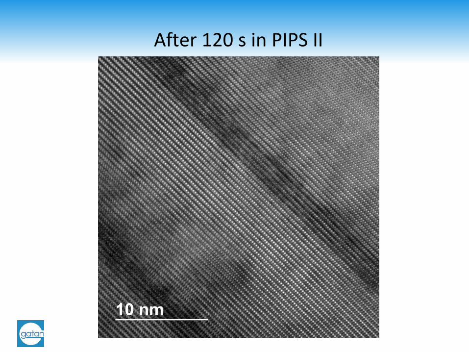
1. Sample prepared in FIB, final milling at 5 keV
2. Sample imaged in TEM
3. Sample was milled in PIPS II:
I. 2 min at 0.1 keV, -80 ⁰ C, ±7⁰ milling angle, Stationary milling mode
4. Sample imaged in TEM
Imaging was done in a FEI TF20 at 200 KV and spot 1, using a Gatan Orius camera.
Work Flow

CONFIDENTIAL (presentation title here)
After FIB After 120 s in PIPS II
Thickness maps Contrast settings are similar for both maps.

CONFIDENTIAL (presentation title here)
After FIB After 120 s in PIPS II

CONFIDENTIAL (presentation title here)
After FIB After 120 s in PIPS II

CONFIDENTIAL (presentation title here)
After FIB After 120 s in PIPS II

CONFIDENTIAL (presentation title here)
After FIB After 120 s in PIPS II
CONFIDENTIAL (presentation title here)
After 120 s in PIPS II

CONFIDENTIAL (presentation title here)
Milling conditions for the clean up:
• Stationary milling mode
• Polish Time : 90 seconds
• Each gun milled separately at 100 eV
• Left gun milled at +7 and right gun milled at -7 degrees
• Temperature: -80° C
The x-y stage in PIPS II made it possible to bring the sample to the rotation center where the guns were aligned.
Imaging in TEM:
• Imaging was done in a FEI TF20 at 200 KV and spot 3, using a single tilt holder and Orius camera.

CONFIDENTIAL (presentation title here)
Area 1 Note : Post FIB Images from Customer’s Titan : Post PIPS Images in Gatan’s TF-20
After FIB After 90 S in PIPS II, 100 eV

CONFIDENTIAL (presentation title here)
Area 1
After FIB After 90 S in PIPS II, 100 eV

CONFIDENTIAL (presentation title here)
Question Which TEM Is Better ? Titan or TF20?
After FIB Titan After 90 S in PIPS II, 100 eV TF-20

CONFIDENTIAL (presentation title here)
What Happens if FIB Only is used ?

CONFIDENTIAL (presentation title here)
And FIB + Broad Ion Beam ?
Thank You


![RUNNING TIME ANALYSIS - GitHub Pages · Running time analysis of the iterative algorithm function F(n) Create an array fib[1..n] fib[1] = 1 fib[2] = 1 for i = 3 to n: fib[i] = fib[i-1]](https://static.fdocuments.us/doc/165x107/5e95ef9e965d8c2b7e7f1cbb/running-time-analysis-github-pages-running-time-analysis-of-the-iterative-algorithm.jpg)