Broad Argon Beam Tools for SEM Prep -...
42
CONFIDENTIAL (presentation title here) Broad Argon Ion Beam Tools for SEM Prep Mike Hassel Shearer 1 & Vikstrom Hakan 2 1 Gatan 2 Oxford Instruments
Transcript of Broad Argon Beam Tools for SEM Prep -...
CONFIDENTIAL (presentation title here)
Broad Argon Ion Beam Tools for SEM Prep
Mike Hassel Shearer1 & Vikstrom Hakan2
1 Gatan
2 Oxford Instruments
CONFIDENTIAL (presentation title here)
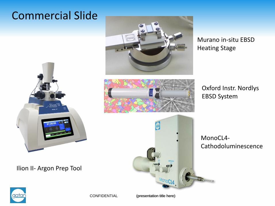
Commercial Slide
Ilion II- Argon Prep Tool
Murano in-situ EBSD Heating Stage
Oxford Instr. Nordlys EBSD System
MonoCL4- Cathodoluminescence
CONFIDENTIAL (presentation title here)
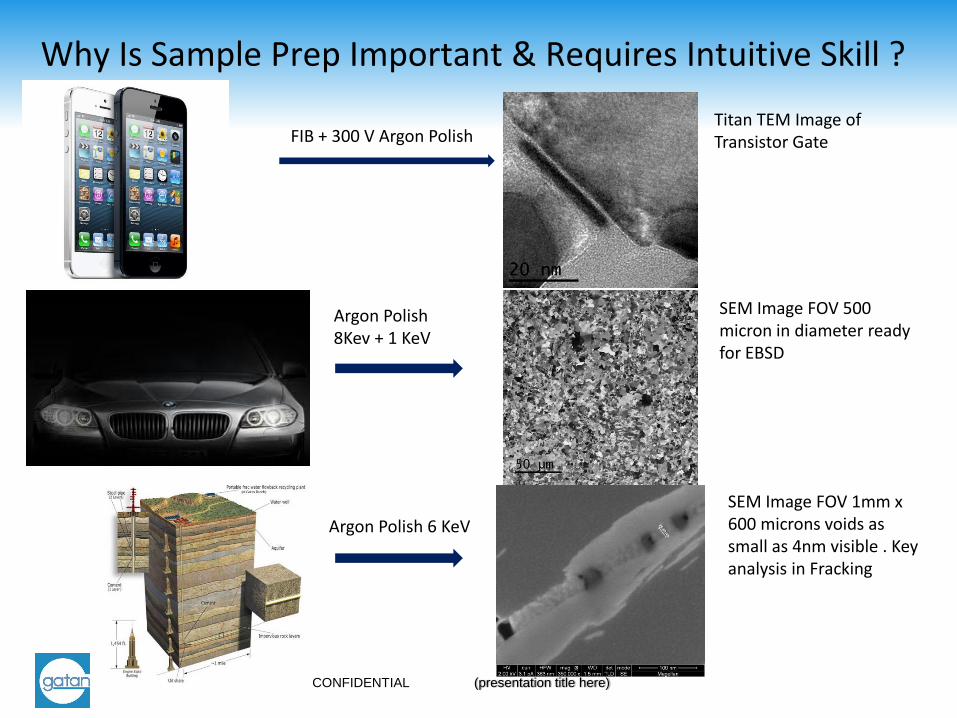
Why Is Sample Prep Important & Requires Intuitive Skill ?
FIB + 300 V Argon Polish
Argon Polish 8Kev + 1 KeV
Argon Polish 6 KeV
Titan TEM Image of Transistor Gate
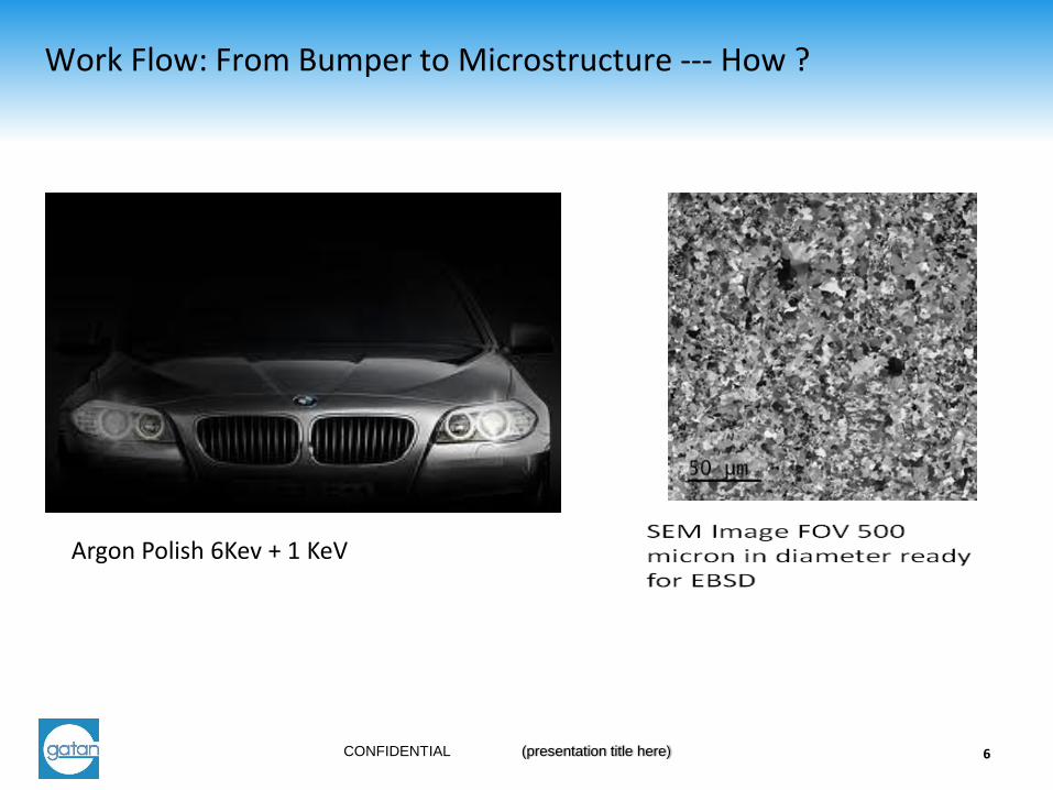
SEM Image FOV 500 micron in diameter ready for EBSD
SEM Image FOV 1mm x 600 microns voids as small as 4nm visible . Key analysis in Fracking
CONFIDENTIAL (presentation title here)
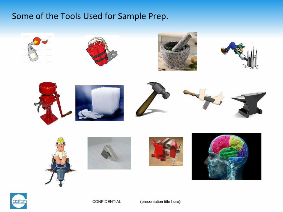
Some of the Tools Used for Sample Prep.
CONFIDENTIAL (presentation title here)
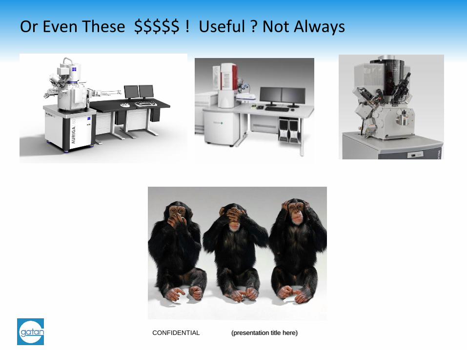
Or Even These $$$$$ ! Useful ? Not Always
CONFIDENTIAL (presentation title here)
Work Flow: From Bumper to Microstructure --- How ?
6
Argon Polish 6Kev + 1 KeV
CONFIDENTIAL (presentation title here)
WorkFlow for Steel and Hard Materials
Outcome:
Large Polished/Undamaged surface to use for grain size and grain orientation analysis in test samples or structural components.
This means using a SEM ( Back-Scattered Image) and EBSD.
Often this work to be done at elevated temperature (Murano).
Issues:
Large Area >500 micron x 500 microns restricts the use of FIB
Mechanical Polish requires skill and every material may require a special process. Additionally the process may require the use of chemicals (acids) to remove final damage layer.
Solution:
Broad Argon Beam Tool (Ilion II) in both cross section or planar mode.
Murano for in-Situ EBSD at Temperature
7
CONFIDENTIAL (presentation title here)
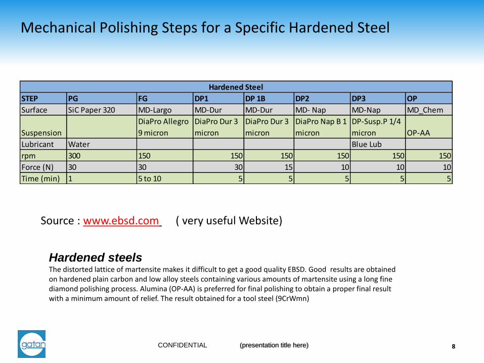
Mechanical Polishing Steps for a Specific Hardened Steel
8
STEP PG FG DP1 DP 1B DP2 DP3 OP
Surface SiC Paper 320 MD-Largo MD-Dur MD-Dur MD- Nap MD-Nap MD_Chem
Suspension
DiaPro Allegro
9 micron
DiaPro Dur 3
micron
DiaPro Dur 3
micron
DiaPro Nap B 1
micron
DP-Susp.P 1/4
micron OP-AA
Lubricant Water Blue Lub
rpm 300 150 150 150 150 150 150
Force (N) 30 30 30 15 10 10 10
Time (min) 1 5 to 10 5 5 5 5 5
Hardened Steel
Source : www.ebsd.com ( very useful Website)
Hardened steels The distorted lattice of martensite makes it difficult to get a good quality EBSD. Good results are obtained on hardened plain carbon and low alloy steels containing various amounts of martensite using a long fine diamond polishing process. Alumina (OP-AA) is preferred for final polishing to obtain a proper final result with a minimum amount of relief. The result obtained for a tool steel (9CrWmn)
CONFIDENTIAL (presentation title here)
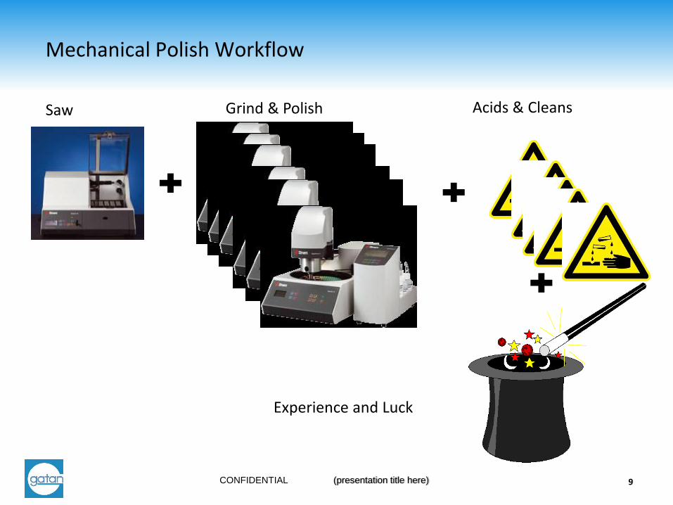
Mechanical Polish Workflow
9
Saw Grind & Polish Acids & Cleans
Experience and Luck
CONFIDENTIAL (presentation title here)
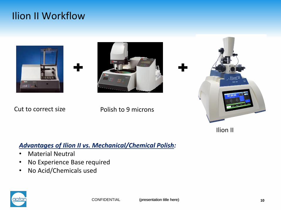
Ilion II Workflow
10
Cut to correct size Polish to 9 microns
Ilion II
Advantages of Ilion II vs. Mechanical/Chemical Polish: • Material Neutral • No Experience Base required • No Acid/Chemicals used
CONFIDENTIAL (presentation title here)
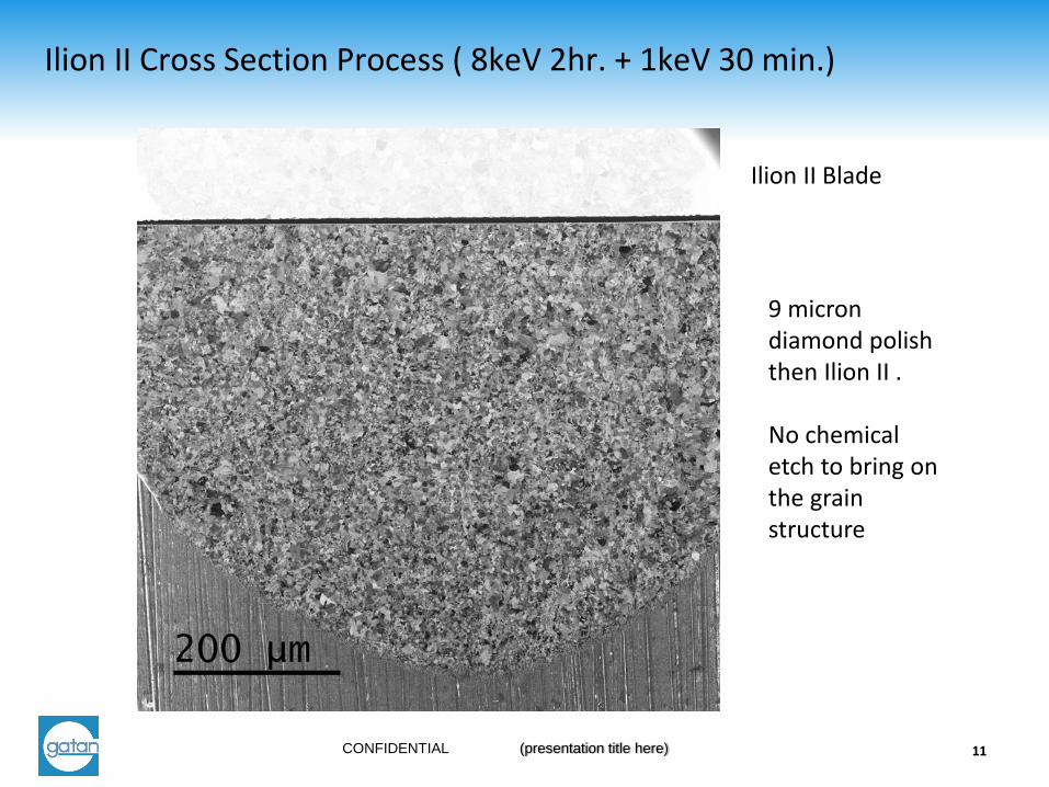
Ilion II Cross Section Process ( 8keV 2hr. + 1keV 30 min.)
11
Ilion II Blade
9 micron diamond polish then Ilion II . No chemical etch to bring on the grain structure
CONFIDENTIAL (presentation title here)
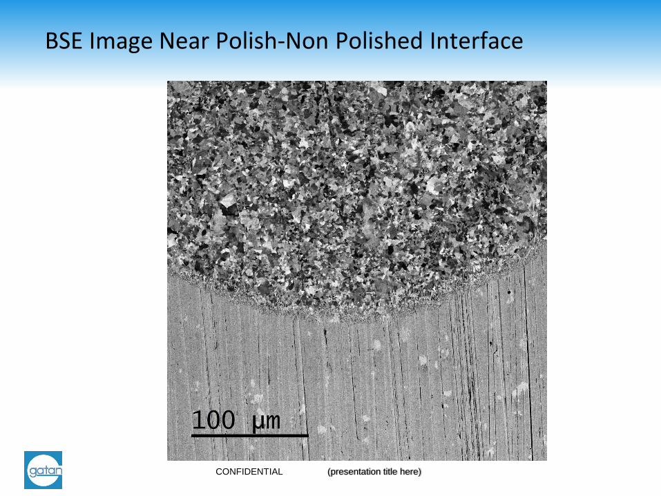
BSE Image Near Polish-Non Polished Interface
CONFIDENTIAL (presentation title here)
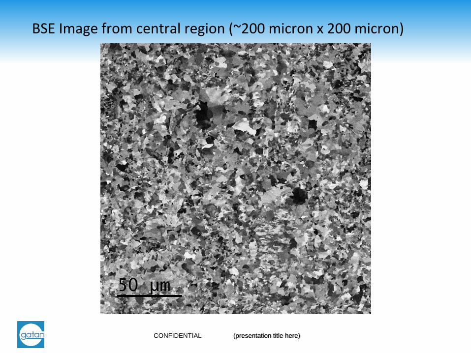
BSE Image from central region (~200 micron x 200 micron)
CONFIDENTIAL (presentation title here)
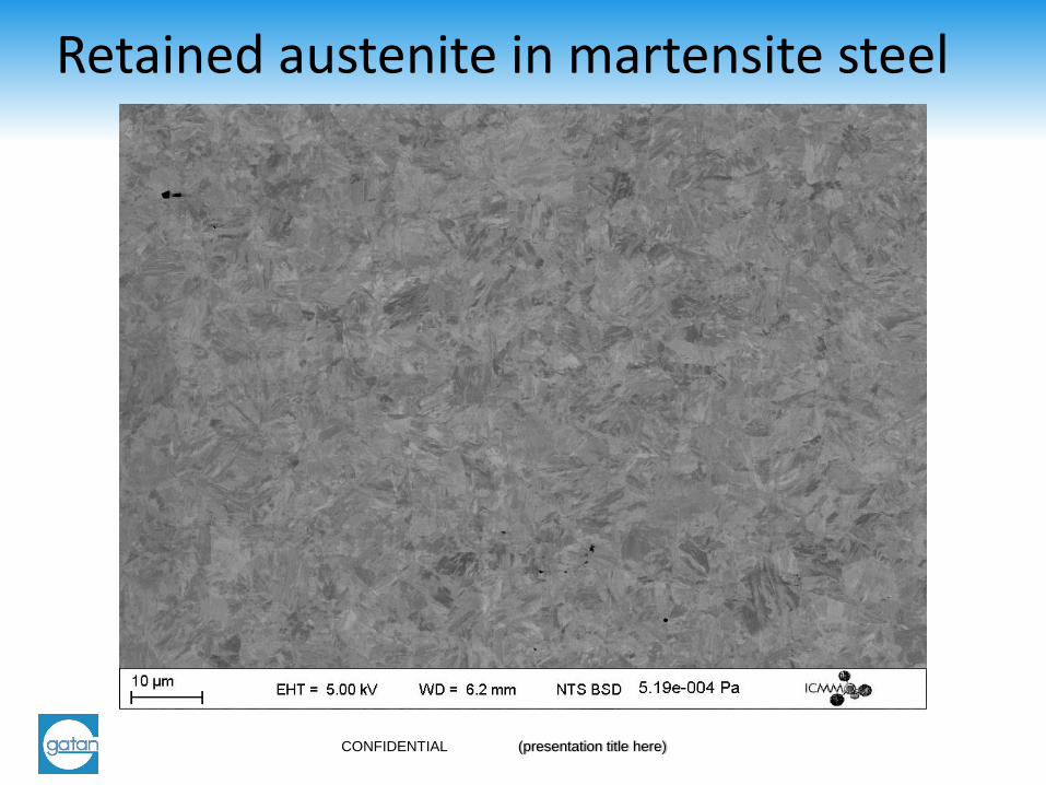
Retained austenite in martensite steel
CONFIDENTIAL (presentation title here)
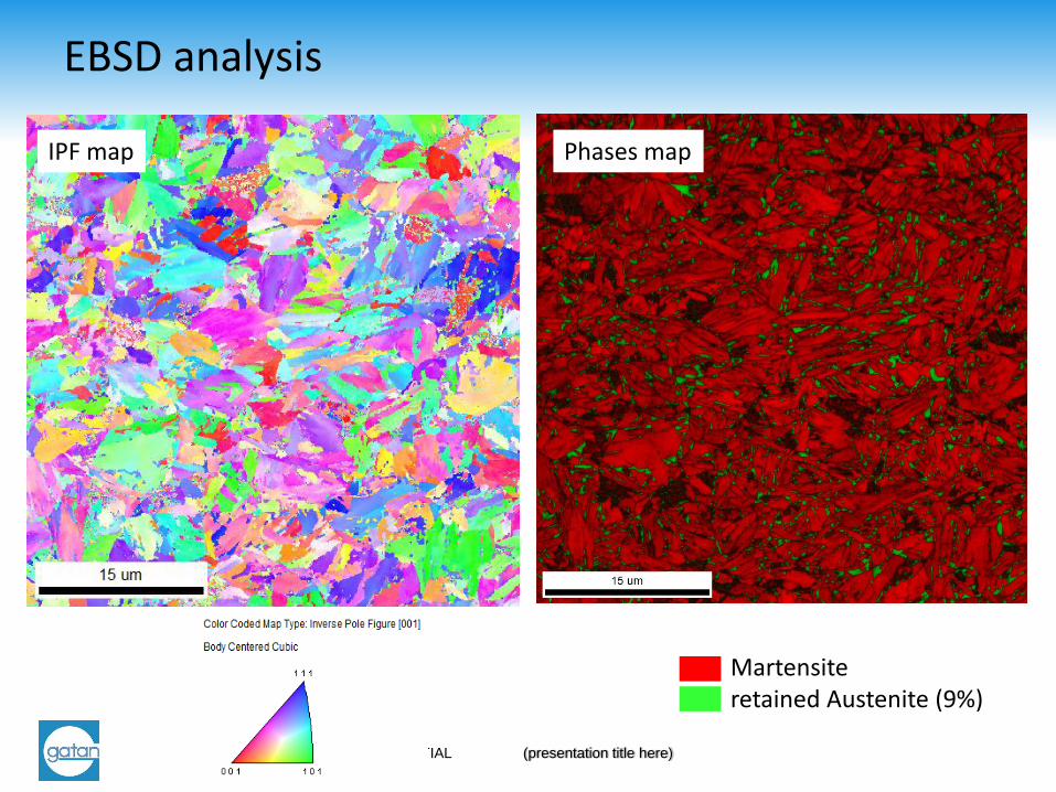
EBSD analysis
IPF
Phases map
Martensite retained Austenite (9%)
IPF map
CONFIDENTIAL (presentation title here)
Affect of Argon Polishing Voltage on EBSD Results
see www.srim.org for details of the effect of Noble Ion Species on Sputtering ( yields, implant, damage) at LOW Voltage
CONFIDENTIAL (presentation title here)
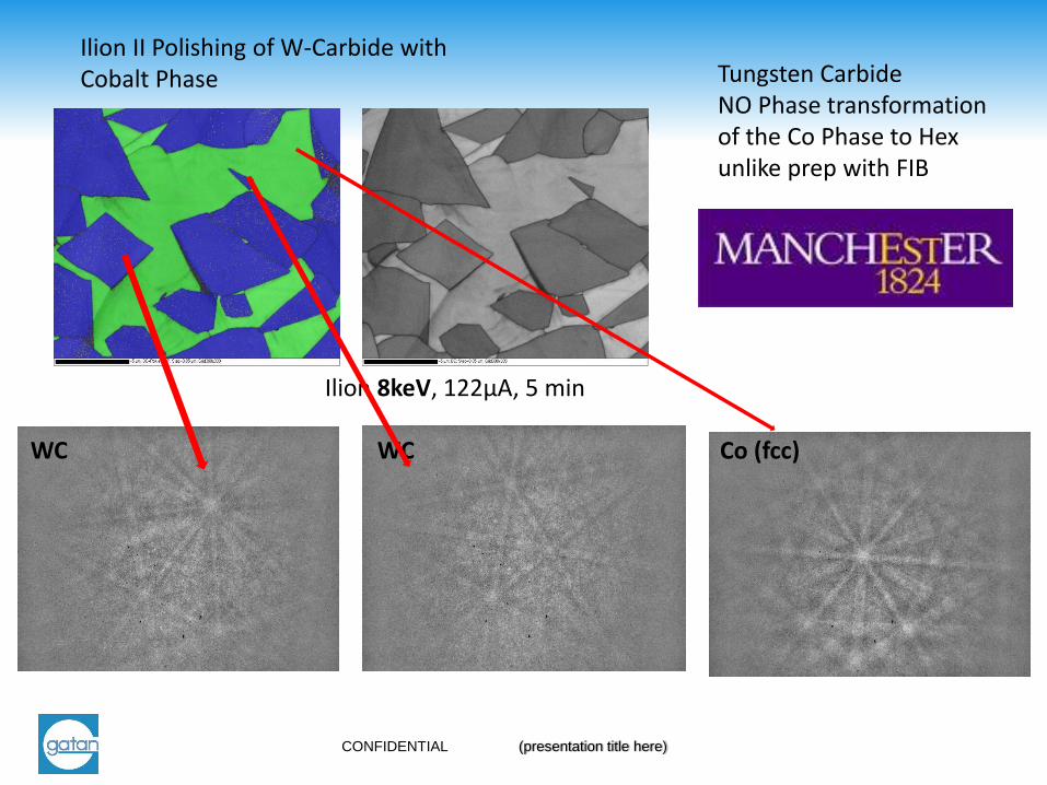
Ilion 8keV, 122μA, 5 min
Tungsten Carbide NO Phase transformation of the Co Phase to Hex unlike prep with FIB
WC WC Co (fcc)
Ilion II Polishing of W-Carbide with Cobalt Phase
CONFIDENTIAL (presentation title here)
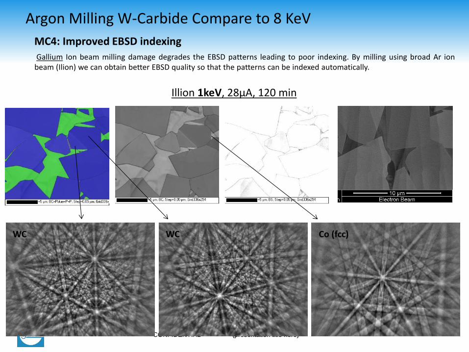
Argon Milling W-Carbide Compare to 8 KeV
MC4: Improved EBSD indexing
Gallium Ion beam milling damage degrades the EBSD patterns leading to poor indexing. By milling using broad Ar ion beam (Ilion) we can obtain better EBSD quality so that the patterns can be indexed automatically.
Illion 1keV, 28µA, 120 min
WC WC Co (fcc)
CONFIDENTIAL (presentation title here)
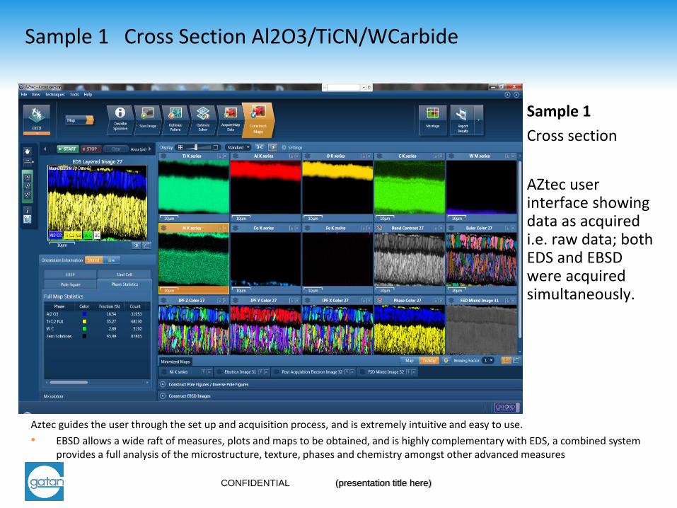
Sample 1
Cross section
AZtec user interface showing data as acquired i.e. raw data; both EDS and EBSD were acquired simultaneously.
Sample 1 Cross Section Al2O3/TiCN/WCarbide
Aztec guides the user through the set up and acquisition process, and is extremely intuitive and easy to use.
• EBSD allows a wide raft of measures, plots and maps to be obtained, and is highly complementary with EDS, a combined system provides a full analysis of the microstructure, texture, phases and chemistry amongst other advanced measures
CONFIDENTIAL (presentation title here)
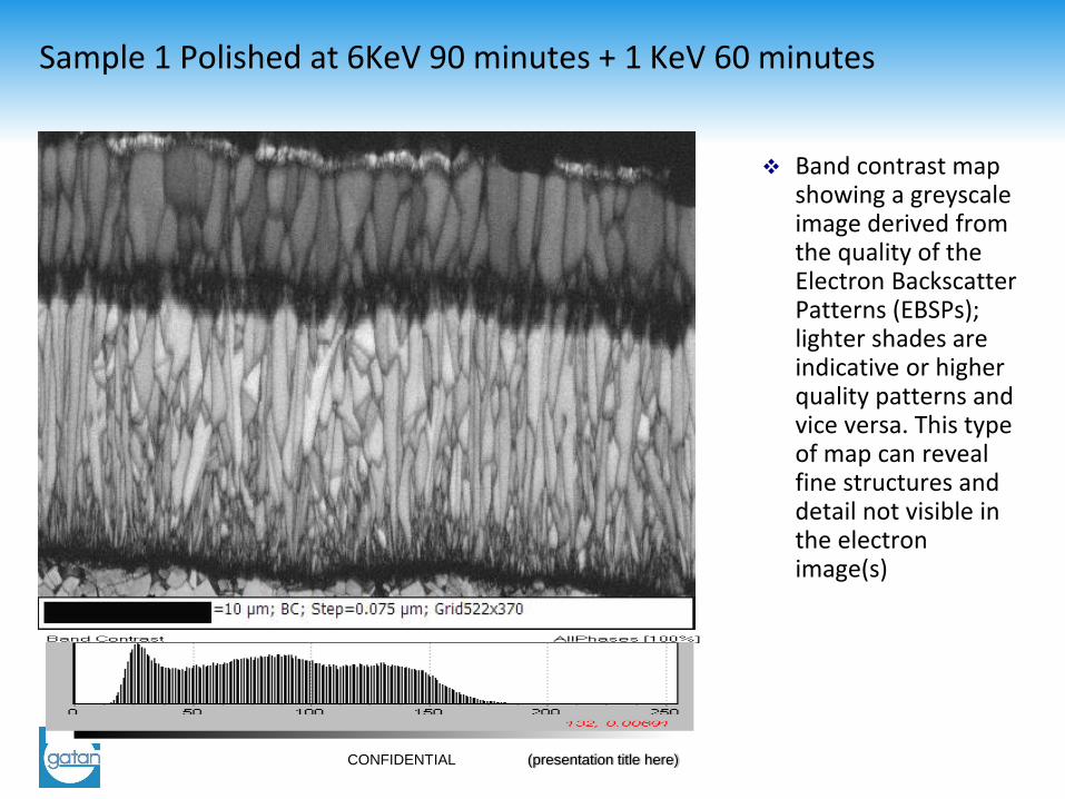
Band contrast map showing a greyscale image derived from the quality of the Electron Backscatter Patterns (EBSPs); lighter shades are indicative or higher quality patterns and vice versa. This type of map can reveal fine structures and detail not visible in the electron image(s)
Sample 1 Polished at 6KeV 90 minutes + 1 KeV 60 minutes
CONFIDENTIAL (presentation title here)
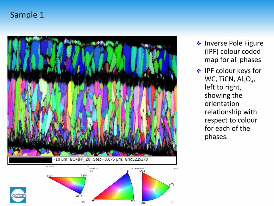
Inverse Pole Figure (IPF) colour coded map for all phases
IPF colour keys for WC, TiCN, Al2O3, left to right, showing the orientation relationship with respect to colour for each of the phases.
Sample 1
CONFIDENTIAL (presentation title here)
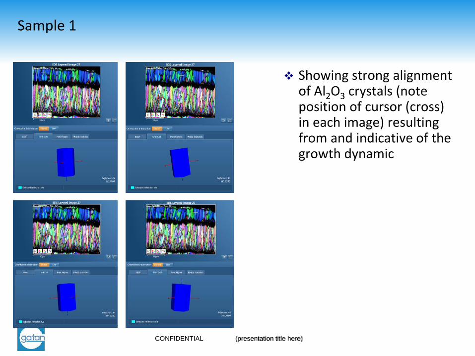
Showing strong alignment of Al2O3 crystals (note position of cursor (cross) in each image) resulting from and indicative of the growth dynamic
Sample 1
CONFIDENTIAL (presentation title here)
EBSD in-Situ at Elevated Temperature
CONFIDENTIAL (presentation title here)
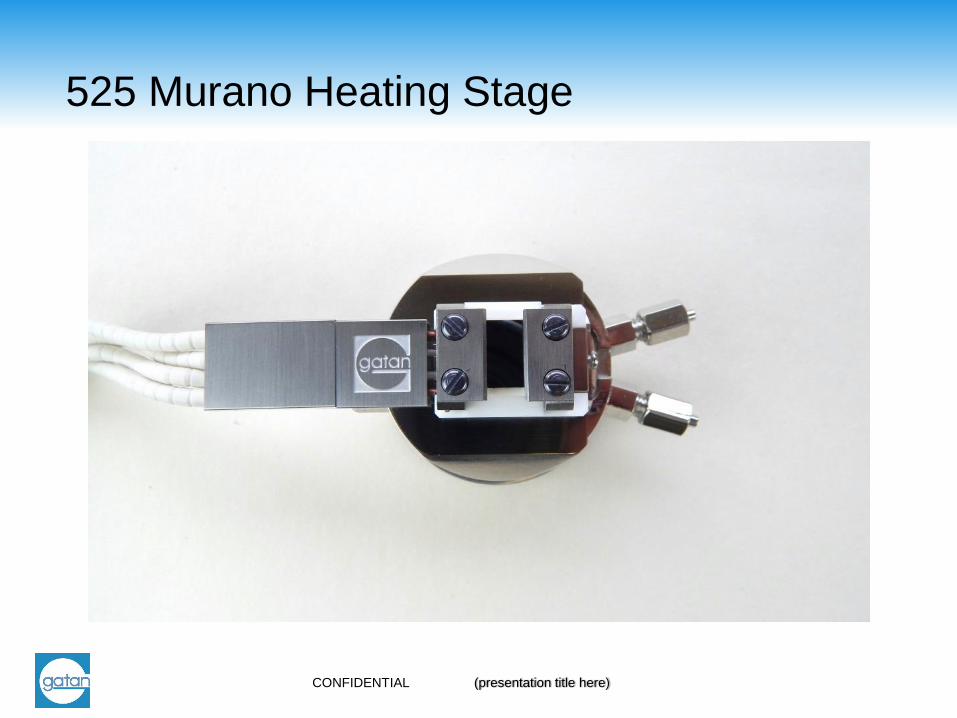
525 Murano Heating Stage
CONFIDENTIAL (presentation title here)
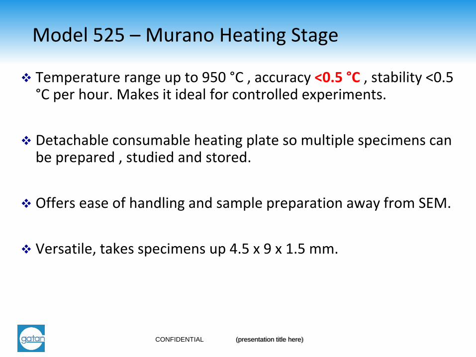
Model 525 – Murano Heating Stage
Temperature range up to 950 °C , accuracy <0.5 °C , stability <0.5 °C per hour. Makes it ideal for controlled experiments.
Detachable consumable heating plate so multiple specimens can be prepared , studied and stored.
Offers ease of handling and sample preparation away from SEM.
Versatile, takes specimens up 4.5 x 9 x 1.5 mm.
CONFIDENTIAL (presentation title here)
Application : Identification - Phase transformation
CONFIDENTIAL (presentation title here)
300 µm
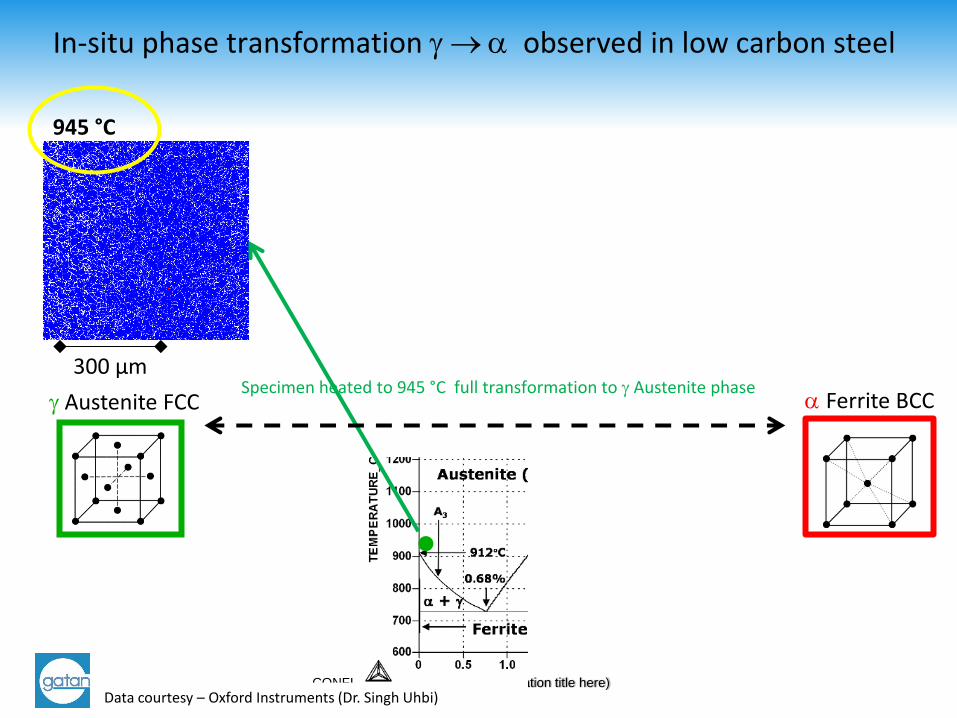
In-situ phase transformation observed in low carbon steel
945 °C
Specimen heated to 945 °C full transformation to Austenite phase Austenite FCC Ferrite BCC
Data courtesy – Oxford Instruments (Dr. Singh Uhbi)
CONFIDENTIAL (presentation title here)
Ferrite BCC
300 µm
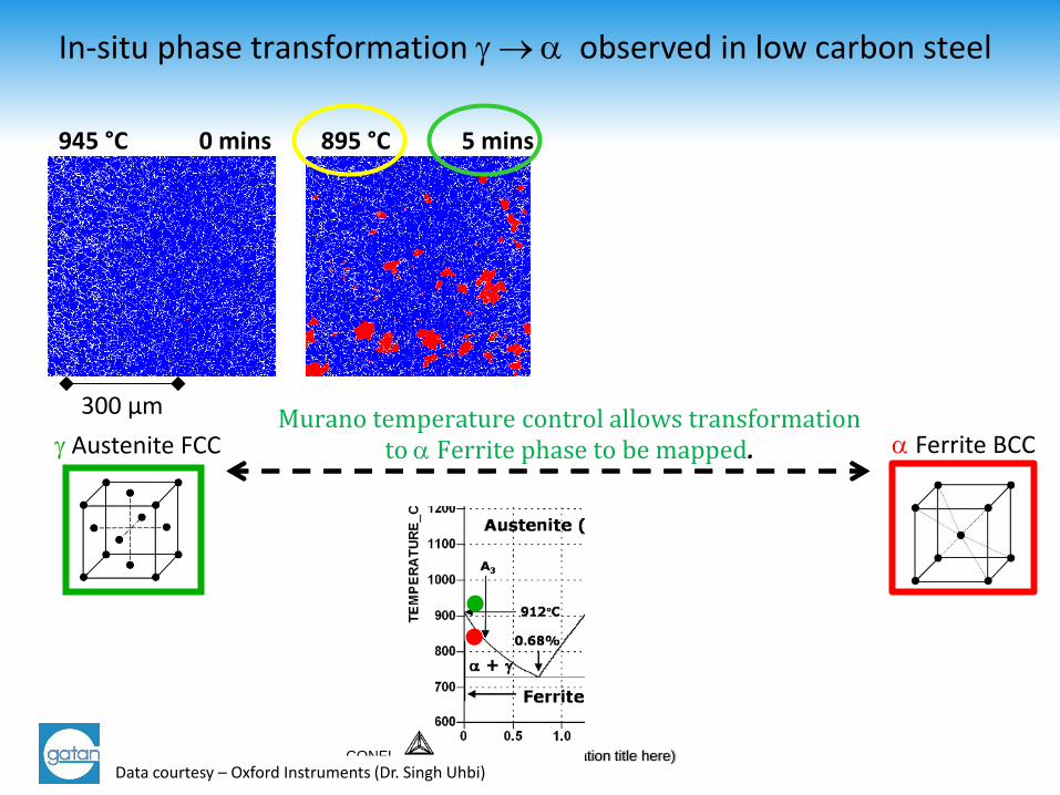
In-situ phase transformation observed in low carbon steel
945 °C 0 mins 895 °C 5 mins
Murano temperature control allows transformation to Ferrite phase to be mapped.
Austenite FCC
Data courtesy – Oxford Instruments (Dr. Singh Uhbi)
CONFIDENTIAL (presentation title here)
Austenite FCC Ferrite BCC
300 µm
In-situ phase transformation observed in low carbon steel
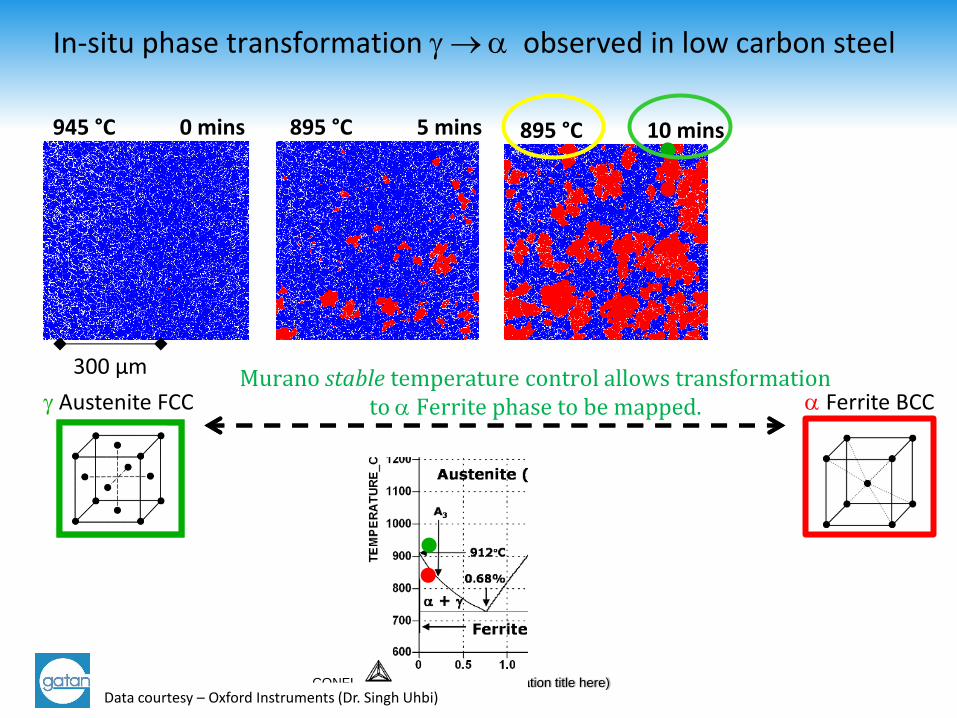
945 °C 0 mins 895 °C 5 mins 895 °C 10 mins
Murano stable temperature control allows transformation to Ferrite phase to be mapped.
Data courtesy – Oxford Instruments (Dr. Singh Uhbi)
CONFIDENTIAL (presentation title here)
Austenite FCC
300 µm
In-situ phase transformation observed in low carbon steel
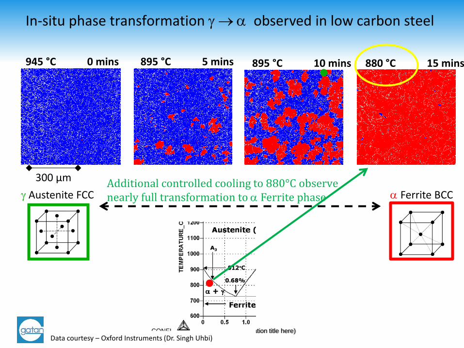
945 °C 0 mins 895 °C 5 mins 895 °C 10 mins 880 °C 15 mins
Additional controlled cooling to 880°C observe nearly full transformation to Ferrite phase Ferrite BCC
Data courtesy – Oxford Instruments (Dr. Singh Uhbi)
CONFIDENTIAL (presentation title here)
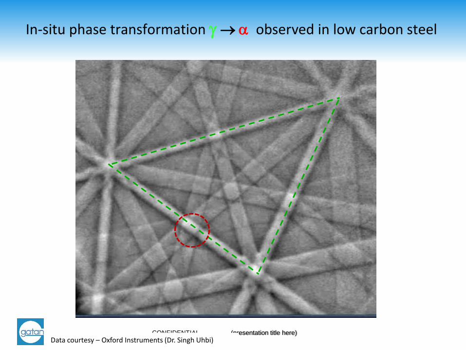
In-situ phase transformation observed in low carbon steel
Data courtesy – Oxford Instruments (Dr. Singh Uhbi)
CONFIDENTIAL (presentation title here)
LED’s Broad Argon Ion Beam + Cathodoluminescence
CONFIDENTIAL (presentation title here)
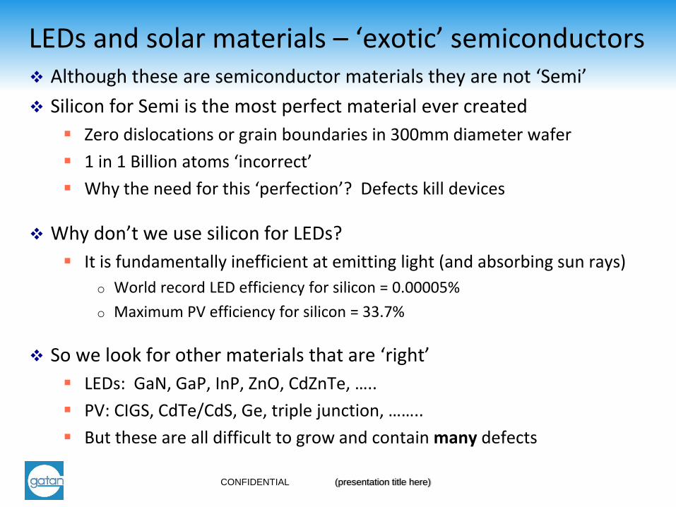
LEDs and solar materials – ‘exotic’ semiconductors Although these are semiconductor materials they are not ‘Semi’
Silicon for Semi is the most perfect material ever created
Zero dislocations or grain boundaries in 300mm diameter wafer
1 in 1 Billion atoms ‘incorrect’
Why the need for this ‘perfection’? Defects kill devices
Why don’t we use silicon for LEDs?
It is fundamentally inefficient at emitting light (and absorbing sun rays)
o World record LED efficiency for silicon = 0.00005%
o Maximum PV efficiency for silicon = 33.7%
So we look for other materials that are ‘right’
LEDs: GaN, GaP, InP, ZnO, CdZnTe, …..
PV: CIGS, CdTe/CdS, Ge, triple junction, ……..
But these are all difficult to grow and contain many defects
CONFIDENTIAL (presentation title here)
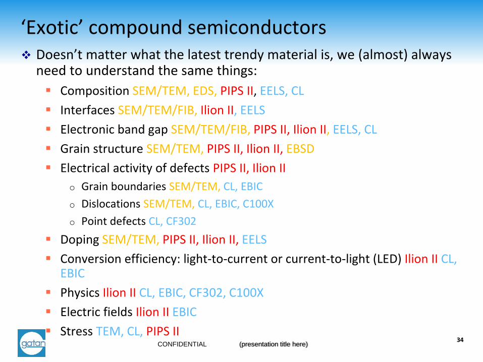
‘Exotic’ compound semiconductors Doesn’t matter what the latest trendy material is, we (almost) always
need to understand the same things:
Composition SEM/TEM, EDS, PIPS II, EELS, CL
Interfaces SEM/TEM/FIB, Ilion II, EELS
Electronic band gap SEM/TEM/FIB, PIPS II, Ilion II, EELS, CL
Grain structure SEM/TEM, PIPS II, Ilion II, EBSD
Electrical activity of defects PIPS II, Ilion II
o Grain boundaries SEM/TEM, CL, EBIC
o Dislocations SEM/TEM, CL, EBIC, C100X
o Point defects CL, CF302
Doping SEM/TEM, PIPS II, Ilion II, EELS
Conversion efficiency: light-to-current or current-to-light (LED) Ilion II CL, EBIC
Physics Ilion II CL, EBIC, CF302, C100X
Electric fields Ilion II EBIC
Stress TEM, CL, PIPS II 34
CONFIDENTIAL (presentation title here)
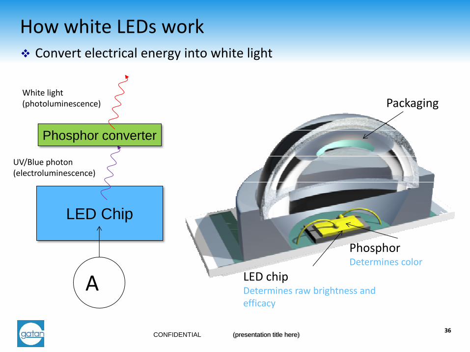
How white LEDs work Convert electrical energy into white light
36
LED Chip
A
Phosphor converter
UV/Blue photon (electroluminescence)
White light (photoluminescence)
LED chip Determines raw brightness and efficacy
Phosphor Determines color
Packaging
CONFIDENTIAL (presentation title here)
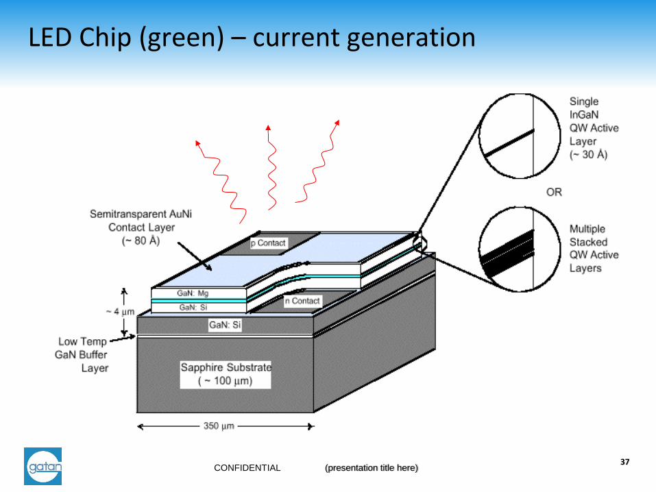
LED Chip (green) – current generation
37
CONFIDENTIAL (presentation title here)
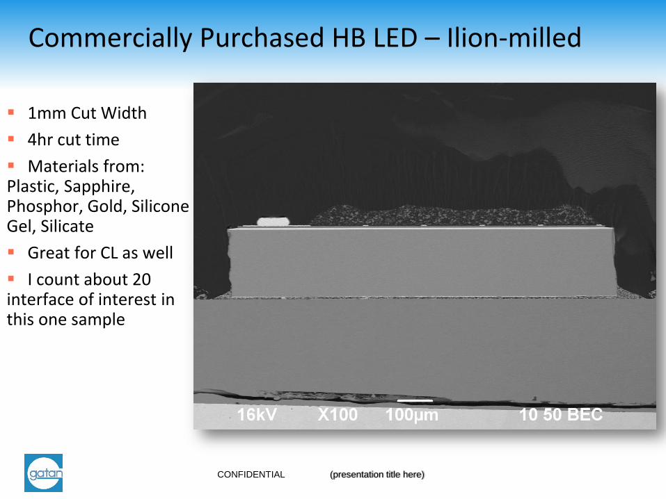
Commercially Purchased HB LED – Ilion-milled
1mm Cut Width
4hr cut time
Materials from: Plastic, Sapphire, Phosphor, Gold, Silicone Gel, Silicate
Great for CL as well
I count about 20 interface of interest in this one sample
CONFIDENTIAL (presentation title here)
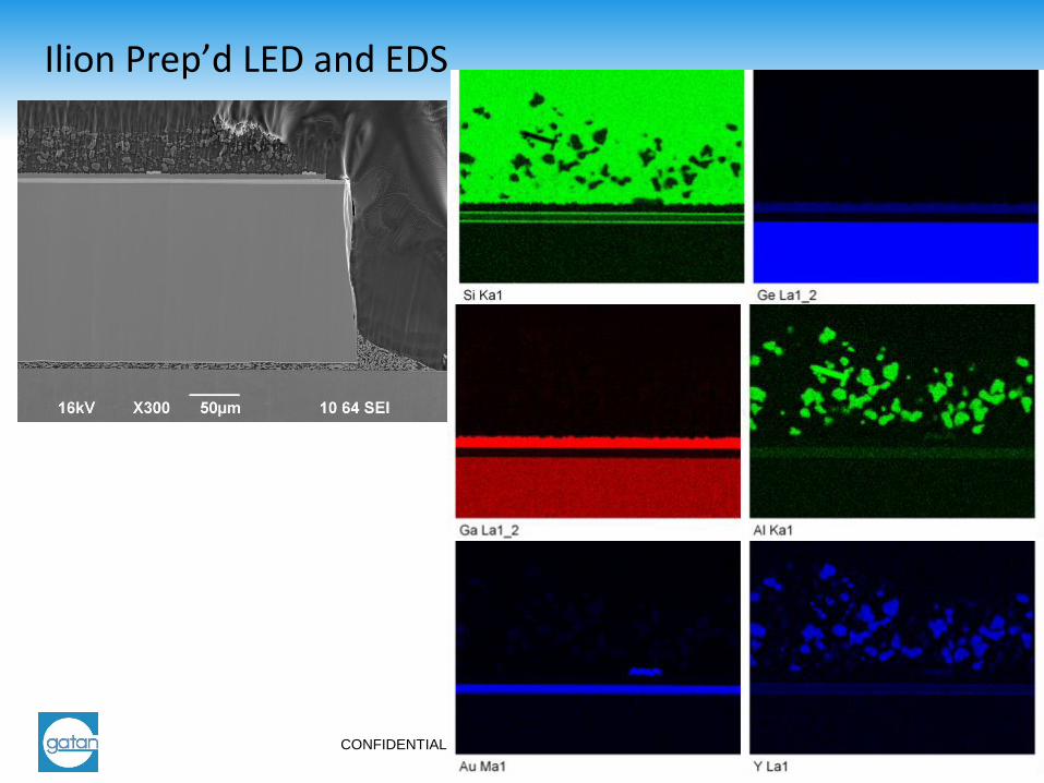
Ilion Prep’d LED and EDS
CONFIDENTIAL (presentation title here)
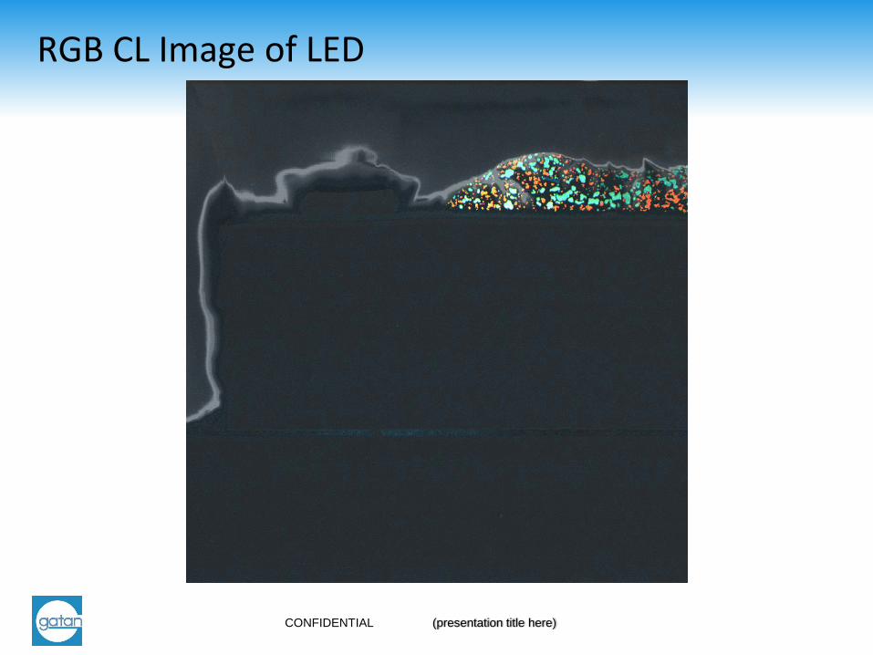
RGB CL Image of LED
CONFIDENTIAL (presentation title here)
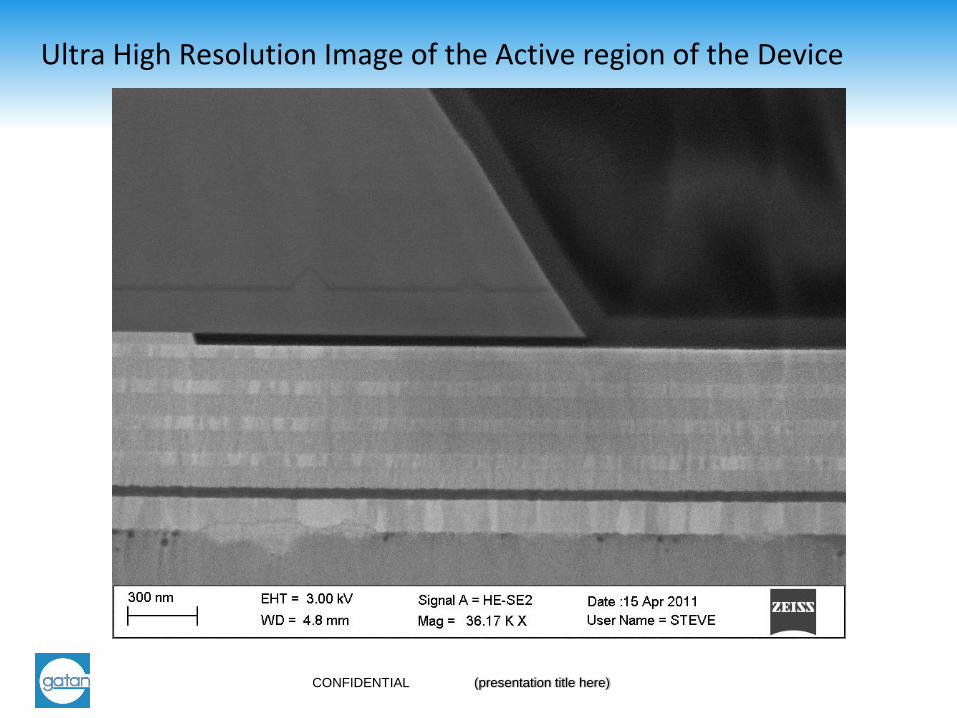
Ultra High Resolution Image of the Active region of the Device
CONFIDENTIAL (presentation title here)
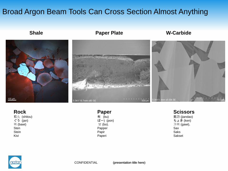
Rock 石头 (shitou)
ぐう (jan)
위 (bawi)
Sten
Stein
Kivi
Paper 布 (bu)
ぱー) (pon)
보 (bo).
Papper
Papir
Paperi
Scissors 剪刀 (jiandao)
ちょき (ken)
가위 (gawi),
Sax
Saks
Sakset
Broad Argon Beam Tools Can Cross Section Almost Anything
Shale Paper Plate W-Carbide
CONFIDENTIAL (presentation title here)
Thank You