1 DC ELECTRICAL CIRCUITS ELECTRONIC TRAINER AND BREADBOARDING.

Breadboarding guide The Board: This guide is intended to provide some general guidance in the use of a solderless breadboard to develop circuits. For this document we will be using the 3M Solderless breadboard Model 309. A diagram can be seen below in figure 1.
ABCDE
FGHIJ
ABCDE
FGHIJ
Y
Z
W
X
Y
Z
W
X
1 5 10 15 20 25 30 35 40 45 50 55 60
Power Binding Posts
ComponentMounting
Board Lead connection hole
Figure 1 - Solderless Breadboard
This type of board consistes of several parts.
• The first of these parts is a metal baseplate. This plate is connected to the black (ground) binding post. This allows for some noise dampening if the circuit is built fairly close to the board.
• The second portion of the board is the binding pose area. This part of the board is typically used to bring power supply leads onto the board. The black is typically ground and the two red posts can be used for other power (i.e. +/- 15VDC). Unscrewing the top of the post reveals a hole used for connecting a discrete wire. Pushing the stripped end of the wire in this hole and tightening down the cap will make a good electrical connection. The top of the post is hollow to accept a banana connector from a power supply.
• The third and most important part is the breadboard itself. This white plastic board contains a series of holes with metal connector strips underneath. This

allows component leads to be pushed into the holes to make contact with other leads and wires. This breadboard area is broken up into two areas
o Power buss strips: rows W,X,Y and X. These are used to supply power to circuit at various points. These strips are usually jumpered to the binding posts by the user. These are joined together internally to form busses. For example Row W columns 3 thru 31 are joined together and Row W column 34 thru 62 are joined to form another buss.
o Component area: rows A-J. These holes are grouped in sets of 5 (column 1 rows A-E, column 1 rows F-J, etc) for placing components and making connections. The layout of the connections can be seen in figure 2. The lines connecting the holes represent the connections made by the metal strips under the plastic.
ABCDE
FGHIJ
ABCDE
FGHIJ
Y
Z
W
X
Y
Z
W
X
1 5 10 15 20 25 30 35 40 45 50 55 60
Figure 2 - Interconnections inside board
Planning a Circuit: The breadboard can be used to develop and test a circuit with a minimum amount of time and effort. There are several basic steps involved in the process successfully building a circuit. These are:
1. Draw a complete schematic before starting, including pin numbers of all devices being used and pin outs of devices such as transistors.
2. Lay out the devices that will be on the board. Be sure to leave plenty of room around the devices for connections and other components, such as capacitors and resistors
3. Connect the needed power busses to the binding posts. Remember to jumper column 31 to 34 if you want the whole buss length available.

4. Keep all components and lead wires as close to the board as possible. 5. Only put one lead in each hole. Multiple wires in a hole will ruin the spring
connection inside and give you an intermittent connection. This will be very hard to find when your circuit doesn’t work.
The circuit for a simple non-inverting operational amplifier (op-amp) circuit can be seen in figure 3. The amplifier selected for this circuit is the National Semiconductor LM741CN plastic dip op-amp. A complete specification sheet can be found in the appendix. This amplifier has the normal inverting (-) input, non-inverting (+) input, output, +V and –V supply lines and also two offset null lines. For this first circuit we will build just a simple un-compensated non-inverting amplifier circuit.
RfR1
-
+ VoutVin
3
2 6
+V power pin 7-V power pin 4
LM741
Figure 3 non-inverting amplifier
The LM741 amplifier shown here resides in a plastic dual inline plastic package as seen in figure 4. Note how the pins on the physical package relate to the functional connections in the schematic. In particular note that the power supply pins do not actually appear in the schematic, but are just a note. If you look in a typical textbook or application note, these pins are assumed and not included in the schematic. Don’t forget to account for them in your design, or your circuit wont work at all. Also note that the plastic dip package will have a notch on one end or a small dimple on the upper left hand corner of the package. This is there to denote the location of pin 1.
Figure 4 Pin layout for LM741CN

The circuit in figure 3 describes a standard non-inverting amplifier circuit. The gain of this amplifier is set by the two resistor values based on the equation
f
ol
ol
in
out
RRRA
AVV
++
=
1
11
where Aol is the open loop gain of the amplifier. For the LM741C the data sheet shows this value to be typically 200. Working this equation out for a nominal value of 10K for R1 and a voltage gain of 20 results in a value of 190K for Rf. Building the Circuit: The first step in building the circuit is to prepare the power supply busses and position the main components. In this case it we will be placing the op-amp in the board and setting up power supplys for +15V, -15V and ground (GND). In this case we will set up row W as +15 volts, Row Y as –15 volts and Rows X and Z as ground. Don’t forget to place the jumpers in at row 30. We have also placed the op-amp in its location at column 40.
ABCDE
FGHIJ
ABCDE
FGHIJ
Y
Z
W
X
Y
Z
W
X
1 5 10 15 20 25 30 35 40 45 50 55 60
+15 -15 GND
Figure 5 Power supply busses and op amp placed on board
Once the main components are in place you can start setting up the connections to the power buss and putting down the smaller components. In this case we need to connect pin 7 to the +15 volt buss and pin 4 to the –15 volt buss. We can also place the resistors R1 (10K ohm) and Rf (190K) in place on the board. Once these two are done then the only remaining step is to bring the input and output points to an easy place to connect to.
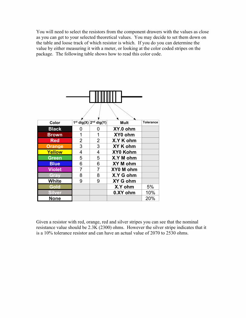
You will need to select the resistors from the component drawers with the values as close as you can get to your selected theoretical values. You may decide to set them down on the table and loose track of which resistor is which. If you do you can determine the value by either measuring it with a meter, or looking at the color coded stripes on the package. The following table shows how to read this color code.
BlackBrown
RedOrangeYellowGreenBlue
VioletGray
GoldSilverNone
White
0123456789
0123456789
XY.0 ohmXY0 ohm
X.Y K ohmXY K ohmXY0 KohmX.Y M ohmXY M ohm
XY0 M ohmX.Y G ohmXY G ohm
1st dig(X) 2nd dig(Y) MultColor Tolerance
5%10%20%
X.Y ohm0.XY ohm
Given a resistor with red, orange, red and silver stripes you can see that the nominal resistance value should be 2.3K (2300) ohms. However the silver stripe indicates that it is a 10% tolerance resistor and can have an actual value of 2070 to 2530 ohms.

ABCDE
FGHIJ
ABCDE
FGHIJ
Y
Z
W
X
Y
Z
W
X
1 5 10 15 20 25 30 35 40 45 50 55 60
+15 -15 GND
Output signalColumn 52 & 54
Input signal29 & 30
R1
Rf
Figure 6 Minor components and wires in place
Figure 7 Actual circuit laid out for testing

The above photograph shows the completed circuit ready for testing. A 1 volt sign wave was fed into the circuit at the Vin point, and the input (pin3), output (pin 6) and feedback (pin 2) were monitored on an oscilloscope. The traces seen below show the signals at these three points.
V p-p 0.98DC Offset -0.012
V p-p 18.4DC Offset -0.2
V p-p 0.972DC Offset -0.036
output (pin 6)
-15-10-505
1015
-0.01 -0.005 0 0.005 0.01
feedback (pin 2)
-0.6-0.4-0.2
00.20.40.6
-0.01 -0.005 0 0.005 0.01
input (pin 3)
-0.6-0.4-0.2
00.20.40.6
-0.01 -0.005 0 0.005 0.01
We can experimentally determine the gain of the circuit by dividing the output peak to peak voltage by the input peak to peak voltage. In this case 18.4 / .98 = 18.8 gain. This

varies from the theoretical primarily due to the resistor tolerance. The actual value of the resistors used were 9.9K and 172.6K ohms, resulting in a theoretical gain of 18.43 based on the actual resistances. We can also se that there is some offset in the output that is undesirable. The LM741 allows for correcting this by adding a potentiometer to pins 1 and 5 as seen in the updated schematic.
RfR1
-
+ VoutVin
3
2 6LM741
Offset10K
-V
15
Figure 8 Offset adjustment
The 10K variable resistor will allow you to trim the output offset out of your circuit. To add this potentiometer we will have to make some minor changes to the circuit. The potentiometer that will be inserted into the circuit has pin relationships as shown in figure 9 and is a 10 turn type trim pot. This device requires 10 turns of the screw to move the wiper from one end of the resistor to the other. Unlike the resistors there is no color code for the resistance value of the potentiometer. The resistance value can be determined by the number on the top of the case. For this device the number is 103, indicating that it’s resistance value is 10, with 3 zeros following, ohms. A 5k would be a 502 and a 100K would read as 104.
Figure 9 Pin relationship for potentiometer
Placing the potentiometer into the board with the first pin in column 33, we have the wiper in column 35 and the second end of the resistance element in column 38. We canwire the wiper (column 35) to –V (row Y
) and the two ends of the resistance element to

pins 1 and 5 of the chip. Figure 10 illustrates the placement and wiring of the pot and associated wiring in the final circuit.
ABCDE
FG
AB
W
X
W
X
+15 -15 GND
Output signalColumn 52 & 54
R1
Rf
HIJ
E
FGHIJ
Y
Z
Y
Z
1 5 10 15 20 25 30 35 40 45 50 55 60
Input signal29 & 30
CD
Figure 10 Circuit layout with offset pot added
Additional Components: There are a number of additional components you may decide to place into your circuit. These include, but are not limited to capacitors, diodes, transistors and inductors. The most common are diodes and capacitors.
zes and styles. Different types have different pplications that they are best suited for. The most common are the “orange drop”,
tors.
anufacturers mark the positive leg while others mark the negative leg of the device. Also some types of capacitors are polarized while others are not. All of these things combine to make capacitors an interesting problem.
Capacitors come in a variety of types, siaceramic, electrolytic, and tantilum. Figure 11 shows exaples of these types of capaci Unlike resistors, there is no single marking system for size or polarity of capacitors. Some capacitors use code systems (104M) to indicate the size while others use spelled out sizes (1000µF), In addition some m

Figure 11 - various types of capacitors
The electrolytic capacitor is a polarized capacitor. These are usually in a can type
ackage with two leads out one end, or an axial package with one lead on each end. The re is a can type 1000µF 50 Volt dc unit. The
negative lead is marked with a dark band and a – sign. The ative lead should always be connected to the more negative al lead. This could be the negative power supply lead or
g
darker component is labeled with a H33. The manufacturer of this component uses this code to denote a 0.33uf 25Volt component. Both pieces also show the markings on the posative leg. The
ppackage shown he
negsignground, depending how it is inserted. Never put the negative lead to the more positive terminal. This can cause the capacitor to explode with a rather vile odor. Another polarized capacitor that you may use frequently is thetantalum capacitor. Like the electrolytic it requires that one lebe placed on a more positive lead. Looking at a closeup of two of these devices you can see that the markings are quite different from the electrolytic. The small size of the package does not
allow for the value to be printed all the way out. For this reason the value is coded in various ways. These two capacitors come from different manufacturers. The tan colored unit is marked witha .1-35 indicating a 35Volt 0.1uf capacitor. The

first part shows this with two plus signs. The manufacturer of the second unit marked it with a single plus sign and a heavy band. They also made the legs different lengths so these could be used with automated machinery. Ceramic and orange drop capacitors are non-polarized. In other words they don’t care which leg is more positive. The different manufacturers have also used different types of markings to show the values.
Both of these devices are 0.01uf capacitors from different manufacturers. One is a higher working voltage (3000V) than the other (25V), and are different physical sizes because of
as used a different type of marking to denote value.
the
band. The band indicateend as shown in the foll the arrow, and blocked in thsheets for the device. L y have a long leg and a fla
nc
p
11/
that. Note that each manufacturer h Diodes come in a multitude of package types sizes and styles. Most are labeled withindustry standard labeling system, that being the part number (such as 1n2002) and a
s the cathode end and relates to the schematic symbol banded owing figure. Note that the current flow is in the direction ofe reverse direction. The voltage drop is specified in the data ight Emitting Diodes (LED’s) are a special case. These usuallt side to indicate the positive leg.
tained in this document will allow you to better can not stress enough how a few extra minutes of ractices can save hours of troubleshooting time.
It is my hope that the information coreate a circuit for you class work. I
preparation and careful construction
Mitchell Cottrell 15/01

LM741Operational AmplifierGeneral DescriptionThe LM741 series are general purpose operational amplifi-ers which feature improved performance over industry stan-dards like the LM709. They are direct, plug-in replacementsfor the 709C, LM201, MC1439 and 748 in most applications.
The amplifiers offer many features which make their applica-tion nearly foolproof: overload protection on the input andoutput, no latch-up when the common mode range is ex-ceeded, as well as freedom from oscillations.
The LM741C is identical to the LM741/LM741A except thatthe LM741C has their performance guaranteed over a 0˚C to+70˚C temperature range, instead of −55˚C to +125˚C.
Connection Diagrams
Typical Application
Metal Can Package
DS009341-2
Note 1: LM741H is available per JM38510/10101
Order Number LM741H, LM741H/883 (Note 1),LM741AH/883 or LM741CH
See NS Package Number H08C
Dual-In-Line or S.O. Package
DS009341-3
Order Number LM741J, LM741J/883, LM741CNSee NS Package Number J08A, M08A or N08E
Ceramic Flatpak
DS009341-6
Order Number LM741W/883See NS Package Number W10A
Offset Nulling Circuit
DS009341-7
August 2000LM
741O
perationalAm
plifier
© 2000 National Semiconductor Corporation DS009341 www.national.com

Absolute Maximum Ratings (Note 2)
If Military/Aerospace specified devices are required, please contact the National Semiconductor Sales Office/Distributors for availability and specifications.
(Note 7)
LM741A LM741 LM741CSupply Voltage ±22V ±22V ±18VPower Dissipation (Note 3) 500 mW 500 mW 500 mWDifferential Input Voltage ±30V ±30V ±30VInput Voltage (Note 4) ±15V ±15V ±15VOutput Short Circuit Duration Continuous Continuous ContinuousOperating Temperature Range −55˚C to +125˚C −55˚C to +125˚C 0˚C to +70˚CStorage Temperature Range −65˚C to +150˚C −65˚C to +150˚C −65˚C to +150˚CJunction Temperature 150˚C 150˚C 100˚CSoldering Information
N-Package (10 seconds) 260˚C 260˚C 260˚CJ- or H-Package (10 seconds) 300˚C 300˚C 300˚CM-Package
Vapor Phase (60 seconds) 215˚C 215˚C 215˚CInfrared (15 seconds) 215˚C 215˚C 215˚C
See AN-450 “Surface Mounting Methods and Their Effect on Product Reliability” for other methods of solderingsurface mount devices.ESD Tolerance (Note 8) 400V 400V 400V
Electrical Characteristics (Note 5)
Parameter Conditions LM741A LM741 LM741C Units
Min Typ Max Min Typ Max Min Typ Max
Input Offset Voltage TA = 25˚C
RS ≤ 10 kΩ 1.0 5.0 2.0 6.0 mV
RS ≤ 50Ω 0.8 3.0 mV
TAMIN ≤ TA ≤ TAMAX
RS ≤ 50Ω 4.0 mV
RS ≤ 10 kΩ 6.0 7.5 mV
Average Input Offset 15 µV/˚C
Voltage Drift
Input Offset Voltage TA = 25˚C, VS = ±20V ±10 ±15 ±15 mV
Adjustment Range
Input Offset Current TA = 25˚C 3.0 30 20 200 20 200 nA
TAMIN ≤ TA ≤ TAMAX 70 85 500 300 nA
Average Input Offset 0.5 nA/˚C
Current Drift
Input Bias Current TA = 25˚C 30 80 80 500 80 500 nA
TAMIN ≤ TA ≤ TAMAX 0.210 1.5 0.8 µA
Input Resistance TA = 25˚C, VS = ±20V 1.0 6.0 0.3 2.0 0.3 2.0 MΩTAMIN ≤ TA ≤ TAMAX, 0.5 MΩVS = ±20V
Input Voltage Range TA = 25˚C ±12 ±13 V
TAMIN ≤ TA ≤ TAMAX ±12 ±13 V
LM74
1
www.national.com 2

Electrical Characteristics (Note 5) (Continued)
Parameter Conditions LM741A LM741 LM741C Units
Min Typ Max Min Typ Max Min Typ Max
Large Signal Voltage Gain TA = 25˚C, RL ≥ 2 kΩVS = ±20V, VO = ±15V 50 V/mV
VS = ±15V, VO = ±10V 50 200 20 200 V/mV
TAMIN ≤ TA ≤ TAMAX,
RL ≥ 2 kΩ,
VS = ±20V, VO = ±15V 32 V/mV
VS = ±15V, VO = ±10V 25 15 V/mV
VS = ±5V, VO = ±2V 10 V/mV
Output Voltage Swing VS = ±20V
RL ≥ 10 kΩ ±16 V
RL ≥ 2 kΩ ±15 V
VS = ±15V
RL ≥ 10 kΩ ±12 ±14 ±12 ±14 V
RL ≥ 2 kΩ ±10 ±13 ±10 ±13 V
Output Short Circuit TA = 25˚C 10 25 35 25 25 mA
Current TAMIN ≤ TA ≤ TAMAX 10 40 mA
Common-Mode TAMIN ≤ TA ≤ TAMAX
Rejection Ratio RS ≤ 10 kΩ, VCM = ±12V 70 90 70 90 dB
RS ≤ 50Ω, VCM = ±12V 80 95 dB
Supply Voltage Rejection TAMIN ≤ TA ≤ TAMAX,
Ratio VS = ±20V to VS = ±5V
RS ≤ 50Ω 86 96 dB
RS ≤ 10 kΩ 77 96 77 96 dB
Transient Response TA = 25˚C, Unity Gain
Rise Time 0.25 0.8 0.3 0.3 µs
Overshoot 6.0 20 5 5 %
Bandwidth (Note 6) TA = 25˚C 0.437 1.5 MHz
Slew Rate TA = 25˚C, Unity Gain 0.3 0.7 0.5 0.5 V/µs
Supply Current TA = 25˚C 1.7 2.8 1.7 2.8 mA
Power Consumption TA = 25˚C
VS = ±20V 80 150 mW
VS = ±15V 50 85 50 85 mW
LM741A VS = ±20V
TA = TAMIN 165 mW
TA = TAMAX 135 mW
LM741 VS = ±15V
TA = TAMIN 60 100 mW
TA = TAMAX 45 75 mW
Note 2: “Absolute Maximum Ratings” indicate limits beyond which damage to the device may occur. Operating Ratings indicate conditions for which the device isfunctional, but do not guarantee specific performance limits.
LM741
www.national.com3

Electrical Characteristics (Note 5) (Continued)
Note 3: For operation at elevated temperatures, these devices must be derated based on thermal resistance, and Tj max. (listed under “Absolute Maximum Rat-ings”). Tj = TA + (θjA PD).
Thermal Resistance Cerdip (J) DIP (N) HO8 (H) SO-8 (M)
θjA (Junction to Ambient) 100˚C/W 100˚C/W 170˚C/W 195˚C/W
θjC (Junction to Case) N/A N/A 25˚C/W N/A
Note 4: For supply voltages less than ±15V, the absolute maximum input voltage is equal to the supply voltage.
Note 5: Unless otherwise specified, these specifications apply for VS = ±15V, −55˚C ≤ TA ≤ +125˚C (LM741/LM741A). For the LM741C/LM741E, these specifica-tions are limited to 0˚C ≤ TA ≤ +70˚C.
Note 6: Calculated value from: BW (MHz) = 0.35/Rise Time(µs).
Note 7: For military specifications see RETS741X for LM741 and RETS741AX for LM741A.
Note 8: Human body model, 1.5 kΩ in series with 100 pF.
Schematic Diagram
DS009341-1
LM74
1
www.national.com 4

Physical Dimensions inches (millimeters) unless otherwise noted
Metal Can Package (H)Order Number LM741H, LM741H/883, LM741AH/883, LM741AH-MIL or LM741CH
NS Package Number H08C
Ceramic Dual-In-Line Package (J)Order Number LM741J/883NS Package Number J08A
LM741
www.national.com5

Physical Dimensions inches (millimeters) unless otherwise noted (Continued)
Dual-In-Line Package (N)Order Number LM741CN
NS Package Number N08E
10-Lead Ceramic Flatpak (W)Order Number LM741W/883, LM741WG-MPR or LM741WG/883
NS Package Number W10A
LM74
1
www.national.com 6

Notes
LIFE SUPPORT POLICY
NATIONAL’S PRODUCTS ARE NOT AUTHORIZED FOR USE AS CRITICAL COMPONENTS IN LIFE SUPPORTDEVICES OR SYSTEMS WITHOUT THE EXPRESS WRITTEN APPROVAL OF THE PRESIDENT AND GENERALCOUNSEL OF NATIONAL SEMICONDUCTOR CORPORATION. As used herein:
1. Life support devices or systems are devices orsystems which, (a) are intended for surgical implantinto the body, or (b) support or sustain life, andwhose failure to perform when properly used inaccordance with instructions for use provided in thelabeling, can be reasonably expected to result in asignificant injury to the user.
2. A critical component is any component of a lifesupport device or system whose failure to performcan be reasonably expected to cause the failure ofthe life support device or system, or to affect itssafety or effectiveness.
National SemiconductorCorporationAmericasTel: 1-800-272-9959Fax: 1-800-737-7018Email: [email protected]
National SemiconductorEurope
Fax: +49 (0) 180-530 85 86Email: [email protected]
Deutsch Tel: +49 (0) 69 9508 6208English Tel: +44 (0) 870 24 0 2171Français Tel: +33 (0) 1 41 91 8790
National SemiconductorAsia Pacific CustomerResponse GroupTel: 65-2544466Fax: 65-2504466Email: [email protected]
National SemiconductorJapan Ltd.Tel: 81-3-5639-7560Fax: 81-3-5639-7507
www.national.com
LM741
OperationalA
mplifier
National does not assume any responsibility for use of any circuitry described, no circuit patent licenses are implied and National reserves the right at any time without notice to change said circuitry and specifications.