Bias Choke - ETH Z
16
Transcript of Bias Choke - ETH Z

Bias Choke
Maryse Ernzer
Semesterthesis, Departement Physik, ETH Zürich
December 14, 2016
Abstract
The bias choke is mainly bulit up of a single layer toroid iron core
inductor used to add two dierent inputs, namely a DC bias and a
high frequency pulse. The essential feature of the nal design consists
in a low cuto frequency of the inductor, a at tranmission with low
attenuation above the cuto frequency, as well as a good temperature
stablility for the device to work at very low temperatures . All of
this properties are important to bias the high frequency pulse without
distorting it. The challenge consists in correctly modeling the behavior
of the inductor as a transmission line in order to remove all resonance
eects from the considered frequency range.
Contents
1 Introduction 2
2 Theory on inductors 2
3 Experimental setup 4
4 Measurements 5
4.1 Toroidal inductors . . . . . . . . . . . . . . . . . . . . . . . . 54.2 SMD inductors . . . . . . . . . . . . . . . . . . . . . . . . . . 13
5 Conclusion 16
6 Bibliography 16
1

1 Introduction
The design of the bias choke aims to apply a DC current to the ux linesinstead of using coils to tune the frequency of the qubits, because of thelimited space on the sample holder underneath the qubit chip. Figure 1shows the insertion of the bias choke into the nal experimental setup.
Figure 1: Circuit diagram of the place-ment of the bias choke in the nal ex-perimental setup
On the one hand the bias chokehas to be very stable and predictablein its transmission and show lit-tle attenuation to precisley tune thequbits. That's why the resonancefeatures, which would allow certainfrequencies to pass through the in-ductor, have to be removed from theconsidered frequency range. Alsothe cuto frequency has to be verylow in order for the inductor to func-tion as an ideal low pass lter and tomaintain the whole microwave pulseon the through line, preventing itfrom leaving through the dc line.
On the other hand the bias chokeneeds to show a steady performanceunder low temperartures as it will
be installed on a 20mK plate. Furthermore the heat production has to beminimzed, considering the limited cooling power available at these temper-atures.
2 Theory on inductors
Measuring the scattering parameters of an inductor one notices resonancepeaks, meaning above the self-resonance frequency one sees dips in the trans-mission which are due to variations in the inductance of the coil. Thesechanges are caused by the reactance of a coil looking like an inductancein parallel with a parasitic capacitance, which makes the inductor an eec-tive LC circuit shown in Figure 2 and generates a self-resonance at fr =1/2π
√LC (SRF). The parasitic capacitances are often explained by the ad-
jacent single windings which are parallel wires functioning as capacitors.This model suggests to use an inductor with a high permeability and as few
2

Figure 2: Schematic equivalent circuit of a real inductor, with L the eectiveinductance, C the parasitic capacitance and R the resistane of the windings[7]
windings as possible to minimize the resonance eects. In fact the lumpedelement predictions are in good agreement with what one sees up to the SRF,but gives no explanation for the additional resonances at higher frequenciesbesides the fundamental SRF. However for higher frequencies where one canno longer consider an electrical circuit as built from lumped elements, thewindings around the coil have to be regarded as a transmission line and theresonances in the inductance as standing waves due to the dierence in themagnetic environment leading to impedance discontinuities as the wire getsaround the coil.
The standing waves produce resonances at wavelengths which are evenmultiples of the path length so that the self-resoance frequency is givenby fr = c
2lpathõ Hz with lpath =
√(Nlp)2 + (αle)2, lp the length of the
periphery of the toroids cross-section, le the length of the magnetic path, αthe fraction of the toroid circumference covered by the winding. [5] Usingthis expression for the SRF which depends only on the dimensions of the coiland the number of windings we can compute the self-capacitance of the coil,as well as the apparent inductance,
Cself = − 1
(2πfr)2L0(1)
with L0 = ALN2 the inductance at low frequencies, (for further explanations
of the inductance factor AL see next section).
Lapp = − XLXC
ω(XL −XC)(2)
3
where XL = ωL0 and XC = 1ωCself
Additional to the parasitic inter-winding capacitance there is also a gapcapacitance, a true capacitance between the emerging wires. For the type ofcoils we use it is about the order of 0.5 pF. That's why the distance betweenthe in and out going wire as well as between the adjacent windings shouldbe maximized. This leads to an optimal opening angle between the in andout going wires of 30 an evenly spread windings.
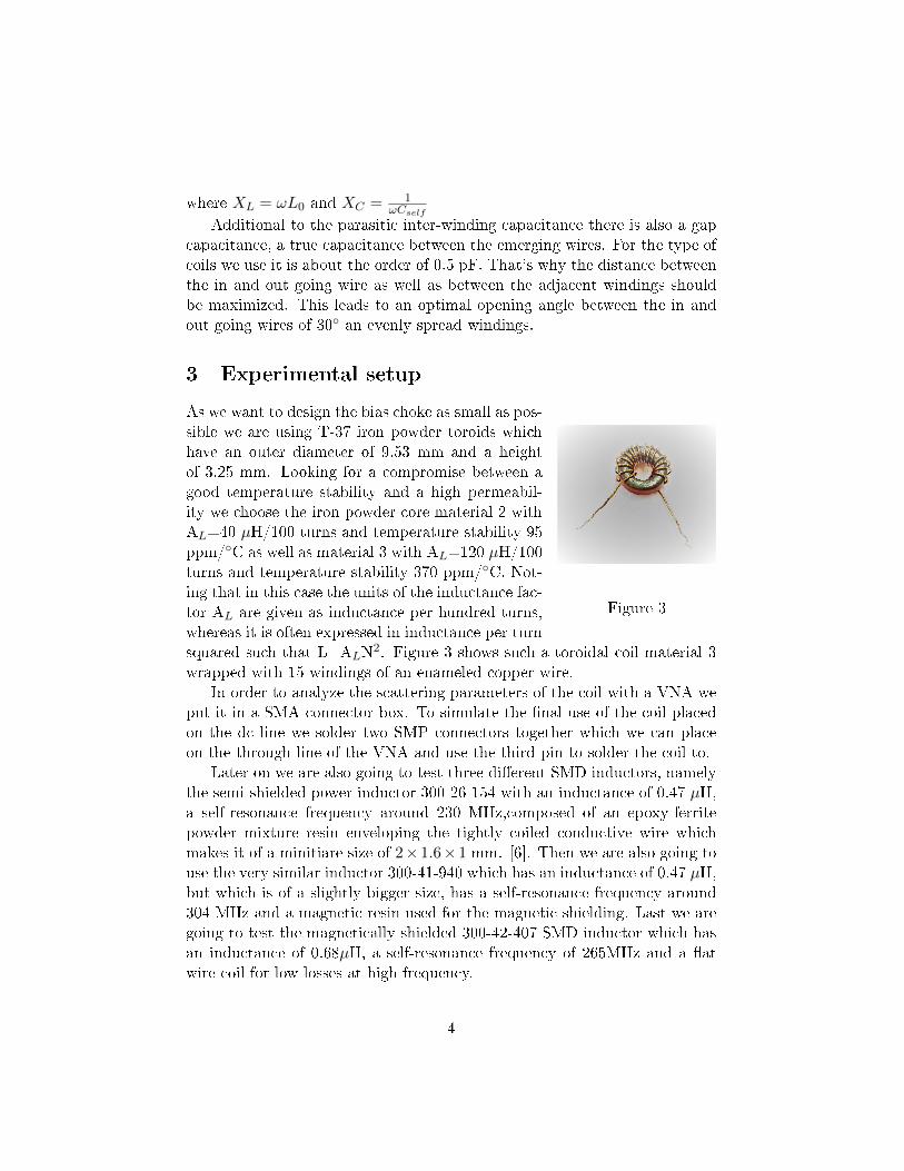
3 Experimental setup
Figure 3
As we want to design the bias choke as small as pos-sible we are using T-37 iron powder toroids whichhave an outer diameter of 9.53 mm and a heightof 3.25 mm. Looking for a compromise between agood temperature stability and a high permeabil-ity we choose the iron powder core material 2 withAL=40 µH/100 turns and temperature stability 95ppm/C as well as material 3 with AL=120 µH/100turns and temperature stability 370 ppm/C. Not-ing that in this case the units of the inductance fac-tor AL are given as inductance per hundred turns,whereas it is often expressed in inductance per turnsquared such that L=ALN2. Figure 3 shows such a toroidal coil material 3wrapped with 15 windings of an enameled copper wire.
In order to analyze the scattering parameters of the coil with a VNA weput it in a SMA connector box. To simulate the nal use of the coil placedon the dc line we solder two SMP connectors together which we can placeon the through line of the VNA and use the third pin to solder the coil to.
Later on we are also going to test three dierent SMD inductors, namelythe semi-shielded power inductor 300-26-154 with an inductance of 0.47 µH,a self-resonance frequency around 230 MHz,composed of an epoxy-ferritepowder mixture resin enveloping the tightly coiled conductive wire whichmakes it of a minitiare size of 2×1.6×1 mm. [6]. Then we are also going touse the very similar inductor 300-41-940 which has an inductance of 0.47 µH,but which is of a slightly bigger size, has a self-resonance frequency around304 MHz and a magnetic resin used for the magnetic shielding. Last we aregoing to test the magnetically shielded 300-42-407 SMD inductor which hasan inductance of 0.68µH, a self-resonance frequency of 265MHz and a atwire coil for low losses at high frequency.
4

4 Measurements
4.1 Toroidal inductors
Figure 4: Schematic quivalent circuit of VNA measurement with ZDUT thedevice under test [4]
First the two SMP connectors are soldered together, shown in Figure 5 us-ing a solder paste and put on the through line, meaning between points 2 and3 in Figure 4 of the VNA. Subsequently it is measured over frequency rangefrom 300 kHz to 1.0 GHz. One can see from Figure 6 that the transmissionshows nearly no attenuation so that it is suitable to join the coil to the highfrequency line in the following measurements.
Figure 5
To see the behavior of the coil 2 with 15 wind-ings separatley, we put it inside a SMA connectorbox, insert it between points 1 and 2 and take ameasurement over a frequency range from 0.03-1.0GHz. From Figure 7 we can see a dierence be-tween the case where the box is closed comparedto the open case, which is due to resonances withinthe box. However in both cases we can observe adip in the transmission around 0.3 GHz which cor-responds to the self-resonance frequency of the coil.The theoretical prediction has been computed usingformulas 3 and 2 and inverting to get an expressionfor S21.
In order to compare our measurement to the
5

Figure 6: Transmission of the two SMP connectors soldered together placedin the through line of the VNA (blue) compared to a standard throughconnector (orange)
Figure 7: Scattering parameter S21 of coil 2 with N=15 windings placedinside a SMA connector box which is once open (blue) and closed (orange),theoretical prediction (black)
6
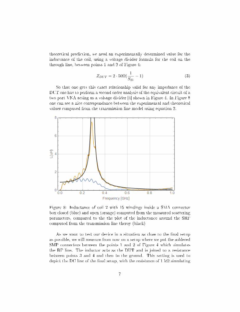
theoretical prediction, we need an experimentally determined value for theinductance of the coil, using a voltage divider formula for the coil on thethrough line, between points 1 and 2 of Figure 4:
ZDUT = 2 · 50Ω(1
S21− 1) (3)
So that one gets this exact relationship valid for any impedance of theDUT one has to perform a second order analysis of the equivalent circuit of atwo port VNA acting as a voltage divider [4] shown in Figure 4. In Figure 8one can see a nice correspondance between the experimental and theoreticalvalues computed from the transmission line model using equation 2.
Figure 8: Inductance of coil 2 with 15 windings inside a SMA connectorbox closed (blue) and open (orange) computed from the measured scatteringparameters, compared to the the plot of the inductance around the SRFcomputed from the transmission line theroy (black)
As we want to test our device in a situation as close to the nal setupas possible, we will measure from now on a setup where we put the solderedSMP connectors between the points 1 and 2 of Figure 4 which simulatesthe RF line. The inductor acts as the DUT and is joined to a resistancebetween points 3 and 4 and then to the ground. This setting is used todepict the DC line of the nal setup, with the resistance of 1 kΩ simulating
7
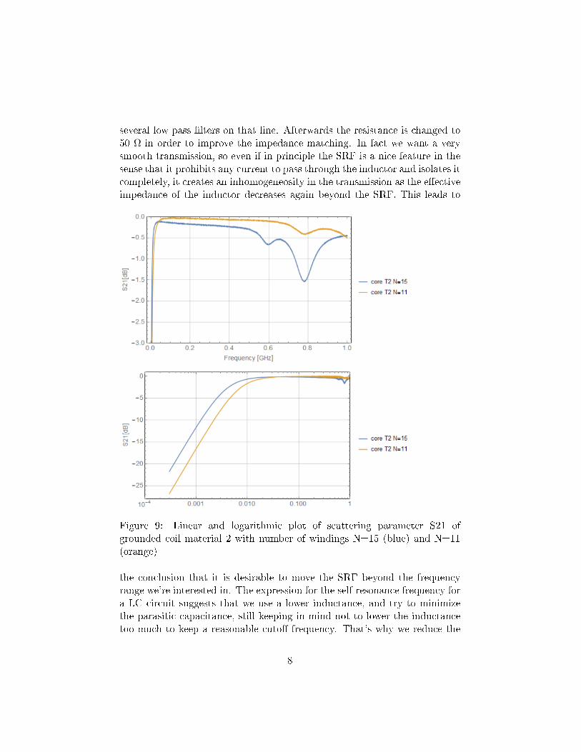
several low pass lters on that line. Afterwards the resistance is changed to50 Ω in order to improve the impedance matching. In fact we want a verysmooth transmission, so even if in principle the SRF is a nice feature in thesense that it prohibits any current to pass through the inductor and isolates itcompletely, it creates an inhomogeneosity in the transmission as the eectiveimpedance of the inductor decreases again beyond the SRF. This leads to
Figure 9: Linear and logarithmic plot of scattering parameter S21 ofgrounded coil material 2 with number of windings N=15 (blue) and N=11(orange)
the conclusion that it is desirable to move the SRF beyond the frequencyrange we're interested in. The expression for the self-resonance frequency fora LC circuit suggests that we use a lower inductance, and try to minimizethe parasitic capacitance, still keeping in mind not to lower the inductancetoo much to keep a reasonable cuto frequency. That's why we reduce the
8

number of windings from N=15 to N=11 and compare the measurementsin Figure 9 where the coil has been directly grounded. The approvementsin the transmission are clearly visible in the linear plot as well as a smalldegradation of the cuto frequency which one can see in the logarithmicplot. We use the standard denition for the cuto frequency consiting ofthe increase of the tranmission to -3dB, which gives us a frequency around3.7 MHz for N=15 and 6.8 MHz for N=11. This provides the motivation toproceed with a coil with higher permeability but fewer windings. To check
Figure 10: Scattering parameter S21 of grounded coil material 2 with numberof windings N=11 (blue) and connected to a 1m wire in between the coil and1 kΩ resistance to the ground (orange)
for the case where the distance between the coil and the resistance we insert asimple wire of 1m length between the coil, between point 3 of Figure 4 and the1kΩ resistance to ground at point 4. The scattering parameter S21 shownin Figure 10 illustrates the perturbations most likely caused by standingwaves on the wire in the transmission, especially for low frequencies. Forhigher frequencies, above the SRF the main feature around 0.8 GHz seemsunchanged, which then must be caused by the wound wire around the coiltogether with the coil itself which sem to oppress the appearance of thestanding waves. One also notices that the increase in Figure 10, arounda frequency of 0.3 GHz corresponds to what one would expect to be theself-resonance frequency of the inductor shown in Figure 8.
As the impedance of the DUT at low frequencies is determined by the
9
additional resistance, one can verify the sensitivity of the measurement byusing the value of the scattering parameter at 300 kHz, S21 = - 0.22 dBtogether with the general formula for the impedance of the device under test(DUT) as shown in Figure 4
ZDUT = 25ΩS21
1− S21(4)
we nd that ZDUT=999.5 Ω which is very close to the 1kΩ that we wouldexpect.
Temperature stability The measurement results of both materials with11 windings mounted on a dipstick in liquid N2 shown in Figure 11 indicatethat, especially for low freuqencies there is a more signicant dierence incomparison to the measurements at room temperature for material 3 thanfor material 2. For all the measurements the calibration of the dipstick hasbeen done at room temperature. The logarithmic plot in Figure 11 alsoillustrates the cuto frequencies. In this case where the coil is connected toa 50 Ω resistance before the ground, we dene the cuto as the frequencyat which the transmission is -1.25 dB because we dene it as half of whatwe expect for the DC case (-3.5 dB) from equation 4 with ZDUT=50Ω. Forcore 2 this leads to a frequency which increases from 22 MHz to 31 MHzwhen it is cooled down in liquid nitrogen. For core 3 with 11 windings thedecrease in temperature changes the frequency from 8 MHz to 16 MHz andfor 8 windings it is 17 MHz at room temperature. All together we can seethat the number of windings of coil 3 can be reduced to 8 in order to improvethe tansmission without changing the inductance too much.
In Figure 15 one can see the scattering parameters of coil 3 with the num-ber of windings reduced to 8 at room temperature, together with the samesetup mounted on a dipstick in liquid helium. The decrease in temperatureincreases the cuto frequency for core T2 from 22 MHz at room temperatureto 27 MHz at 4 K and for core T3 from 15MHz to 40 MHz. This gure alsoclearly shows that the temperature stability of the core T2 is far better thanthat of the core T3.
Additionally we notice the tendency of the S21 scattering parameter, es-pecially for Coil 3 to increase progressiveley with higher frequencies above 0dB. It seems sensible that this eect is due to an overcompensation of theimproved conductivity at low temperatures of the dipstick which we cali-brated at room temperature. This motivates the measurement of a dipstickwith a through connector only in liquid Helium which, shown in Figure 13conrms this assumption. From now on the scattering parameters at low
10

Figure 11: Linear and logarithmic plot of scattering parameter S21 of thecoils grounded to 50 Ω resistance with number of windings N=11 material 2(blue) in liquid nitrogen and at room temperature(dashed), material 3 N=11(orange) in liquid nitrogen and at room temperature (dashed) and material3 N=8 at room temperature (black)
temperatures will be rescaled accordingly and the dierence between theoriginal and the rescaled data is illustrated in Figure 14 which shows a smallbut distinguishable improvement.
11

Figure 12: Scattering parameter S11 of Core T2 (blue) with number ofwindings N=11, and Core T3 (orange) with N=8 both grounded to a 50 Ωresistance at room temperature and in liquid Helium (dahed blue, lighterorange)
Assuming that the temperature dependent variable is in fact the relativepermeability of the iron powder core, the change in inductance of the toroidcan be determined from the displacement of the SRF from room temperatureto 4 K visible in the S11 plot in Figure 12 using fr = 1/2π
√LC, and we
nd LCoil3,300K=0.77µH and LCoil3,4K=0.26µH. The inductance can also beestimated from the S21 parameter using the expression 4 with ZDUT = 50Ω+iwL. At a decline of -1.5dB from the maximal transmission one nds theinductances LCoil3,300K=0.84µH and LCoil3,4K=0.31µH which means thatboth methods provide similar results. If we repeat both this calculationswe nd from the displacmenet of the SRF that LCoil2,300K=0.629µH andLCoil2,4K=0.483µH which is a much smaller change than it was for Coil 3. Ifwe use the method of the attenuation of the S21 parameter we nd similarilyLCoil2,300K=0.55µH and LCoil2,4K=0.48µH which again is consistent withthe theoretical prediction for low frequencies, and with the result of the SRFdisplacement.
12

Figure 13: Scattering parameter S21 of the dipstick calibrated at room tem-perature, measured with a through connector at T=4K (blue) and at roomtemperature (orange)
Figure 14: Scattering parameter S21 of Core T2 with number of windingsN=11 (blue) and Core T3 with N=8 (red), both grounded to a 50 Ω resistancein liquid Helium rescaled and raw data (dashed)
4.2 SMD inductors
Measuring th scattering parameters of the SMD inductors in the same way asfor the coils, soldering them to a 50 Ω resistance and to the SMP connectors,
13
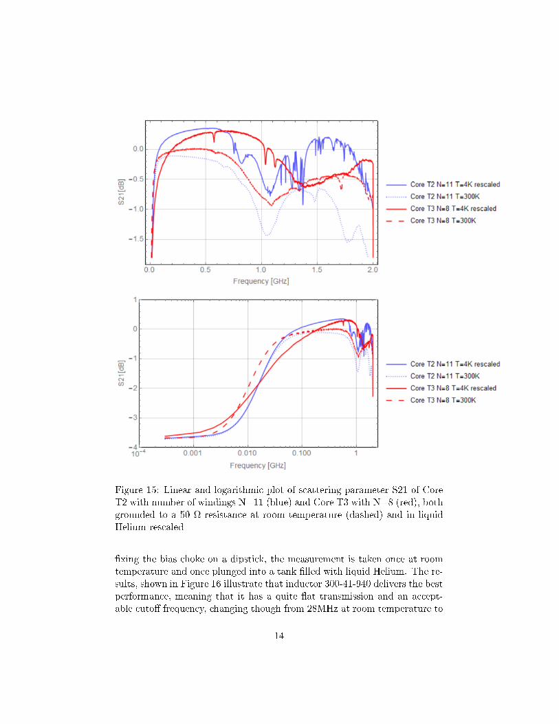
Figure 15: Linear and logarithmic plot of scattering parameter S21 of CoreT2 with number of windings N=11 (blue) and Core T3 with N=8 (red), bothgrounded to a 50 Ω resistance at room temperature (dashed) and in liquidHelium rescaled
xing the bias choke on a dipstick, the measurement is taken once at roomtemperature and once plunged into a tank lled with liquid Helium. The re-sults, shown in Figure 16 illustrate that inductor 300-41-940 delivers the bestperformance, meaning that it has a quite at transmission and an accept-able cuto frequency, changing though from 28MHz at room temperature to
14
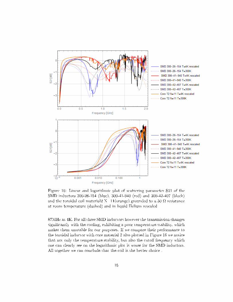
Figure 16: Linear and logarithmic plot of scattering parameter S21 of theSMD inductors 300-26-154 (blue), 300-41-940 (red) and 300-42-407 (black)and the toroidal coil material2 N=11(orange) grounded to a 50 Ω resistanceat room temperature (dashed) and in liquid Helium rescaled
87MHz at 4K. For all three SMD inductors however the transmission changessignicantly with the cooling, exhibiting a poor temperature stability, whichmakes them unusable for our purposes. If we compare their performance tothe toroidal inductor with core material 2 also plotted in Figure 16 we noticethat not only the temperature stability, but also the cuto frequency whichone can clearly see on the logarithmic plot is worse for the SMD inductors.All together we can conclude that the coil is the better choice .
15

5 Conclusion
Comparing all the measurements for both the coils and the SMD inductorstogether we can conclude that overall the toroidal inductors have a bettertemperature stability than the SMD inductors. Also it is advantageous touse as few windings as the cuto frequency allows in order to minimize theparasitic capictances which tamper the low pass lter performance of thecoil. Even if this criterium would favour us to choose T-37 iron powdertoroids with material 3, the crucial argument remains the temperature sta-bility which makes the T-37 iron powder toroids with material 2 preferable.
6 Bibliography
References
[1] Bias Tee 2.0 Daniel Staudigel
[2] The Self-Capacitance of Toroidal Inductors © D W Knight 2008, 2015,2016
[3] The self-resonance and self-capacitance of solenoid coils: applicable the-ory, models and calculation methods. By David W Knight
[4] Agilent Ultra-Low Impedance Measurements Using 2-Port MeasurementsApplication Note
[5] The self-capacitance of single layer toroidal inductors with ferrite cores© Alan Payne 2015
[6] www.distrelec.ch
[7] Eavluate Your 3D Inductor Design with COMSOL Multiphysics, ComsolBlog, Scott Smith, 19 April 2016
16