
BHASKAR POOJARI DESIGN OF A 2.4 GHZ ISM BAND POWER …
96
Transcript of BHASKAR POOJARI DESIGN OF A 2.4 GHZ ISM BAND POWER …
BHASKAR POOJARI
DESIGN OF A 2.4 GHZ ISM BAND POWER DIVIDER WITH
HIGHLY LINEAR SMALL-SIGNAL RF AMPLIFIER
Master of Science Thesis
Examiners: Dr.Jouko Heikkinen and
Adj. Prof. Riku Mäkinen
Examiners and topic approved by the
Faculty Council of the Faculty of Com-
puting and Electrical Engineering on 4
September 2013
II
ABSTRACT
TAMPERE UNIVERSITY OF TECHNOLOGY
Master's Degree Programme in Electrical Engineering
POOJARI, BHASKAR: Design of a 2.4 GHz ISM band Power Divider with
Highly Linear Small-Signal RF Amplier
Master of Science Thesis, 77 pages, 7 Appendix pages
October 2013
Major: Radio Frequency Electronics
Examiners: Dr. Jouko Heikkinen and Adj. Prof. Riku Mäkinen
Keywords: ISM, power divider, linearity, small-signal, RF amplier
This thesis report presents the design of a 2.4 GHz ISM band power divider with
highly linear small-signal RF amplier. The RF amplier is used for compensating
power loss caused as a result of a division operation. The prototyped power divider is
used for the re-design of small-signal board that is utilized in the solid state cooking
project with which required RF input signal is generated and supplied to the high
power amplier. With the re-designed small-signal board it is possible to congure
the system as a single channel system or multichannel master/slave system. The
prototyped power divider has two inputs (LO input and auxiliary input) and three
outputs (Out 1, Out 2, and auxiliary output) with an unequal gain between the input
and output ports. Although multiple power dividers are available in the market, we
aimed to design a low cost power divider by making use of inexpensive components
providing high performance. The prototyped power divider has the possibility for
the mass production.
The objective of the thesis is to fabricate 3-and 2-way power dividers and highly
linear small-signal RF ampliers as standalone devices and then to realize the nal
power divider by integration of the dividers and ampliers. The resistive power
divider topology was chosen for the 3-and 2-way power dividers fabrication because
of its advantages like, easy to implement, compact, and inexpensive. The specied
gain design procedure was followed in the design of the RF ampliers.
The prototyped 3-and 2-way power dividers have insertion loss of 9.88 dB and
6.26 dB respectively and minimum return loss of 21.7 dB is available in the operating
frequency band, 2.4 - 2.5 GHz. The fabricated ampliers are unconditionally stable
up to 18 GHz. The input and output return loss of 17 dB and 10 dB gain ampliers
are 12.5 dB, 21.5 dB and 12.5 dB, 30.5 dB respectively with the power consumption
of 66 mW. The gains are 17.2 dB and 11.2 dB, OIP3 of 29 dBm and 18 dBm
respectively. The prototyped power divider has maximum gain between the inputs
and Out 1 is 0.4 dB, Out 2 and auxiliary output is 1.24 dB. The return loss at all
the input and output ports are above 19 dB. The price of all components is 3.5 euro.
The prototyped power divider is good enough for the application.

III
PREFACE
This thesis report elaborates the work process of my nal step towards getting a
master's degree in Electrical Engineering from Tampere University of Technology,
Finland. This thesis work has been carried out in RF Power and Base Stations
department at NXP Semiconductors, Nijmegen, Netherlands as a part of the Solid
State Cooking project from February 2013 - July 2013. This work has been super-
vised by Klaus Werner and Robin Stenfert. I would like to thank Dr. Klaus Werner,
Program Manager, for giving me an opportunity to work on my thesis and for his
continuous guidance, attention, comments, and mentorship from the beginning to
the end
I would like to thank Mr. Robin Stenfert, Project Manager, Solid State Cooking
project. The work maintained its speed due to his support, for keeping track of my
progress, and providing good working environment (introducing to new people and
providing tools) during the entire period. I am thankful to Mr. Wilfried Schmidt,
RF technician for his support in printed circuit board (PCB) milling. Furthermore,
I would like to appreciate Mr. Joop de Sluis, Mr. Klaas de Waal, and the rest of my
colleagues for their advice, valuable insights, participating in discussions, helping
me in the measurements, and support during this memorable period.
I am grateful to my examiners Dr. Jouko Heikkinen and Adj. Prof. Riku Mäki-
nen at Tampere University of Technology for their valuable advice and comments. I
would like to appreciate the support provided by Riku Mäkinen in the registration
process and nalizing the thesis.
I would like to show my sincere gratitude to my parents and my brother for their
constant support, love, guidance, and motivation throughout my life. Last but not
least, special regards to all who helped me in any form to complete my work.
Tampere, September 2013
Bhaskar Poojari
224008
IV
TABLE OF CONTENTS
1. INTRODUCTION . . . . . . . . . . . . . . . . . . . . . . . . . . . . . . . . 1
1.1 Motivation . . . . . . . . . . . . . . . . . . . . . . . . . . . . . . . . . 3
1.2 Objectives and Scope of the Thesis . . . . . . . . . . . . . . . . . . . . 3
1.3 Thesis Outline . . . . . . . . . . . . . . . . . . . . . . . . . . . . . . . 4
2. BASICS OF RELATED RF CONCEPTS . . . . . . . . . . . . . . . . . . . 5
2.1 Scattering Parameters . . . . . . . . . . . . . . . . . . . . . . . . . . . 5
2.2 Stability . . . . . . . . . . . . . . . . . . . . . . . . . . . . . . . . . . . 8
2.2.1 General Concept . . . . . . . . . . . . . . . . . . . . . . . . . . . . 9
2.2.2 Stability Factors . . . . . . . . . . . . . . . . . . . . . . . . . . . . 10
2.2.3 Stability Circles . . . . . . . . . . . . . . . . . . . . . . . . . . . . 10
2.3 Power Gain Relations and Gain Circles . . . . . . . . . . . . . . . . . . 13
2.4 Impedance Matching Networks . . . . . . . . . . . . . . . . . . . . . . 14
2.5 DC Bias Circuits . . . . . . . . . . . . . . . . . . . . . . . . . . . . . . 16
2.6 Non-linearities in Ampliers . . . . . . . . . . . . . . . . . . . . . . . . 18
2.6.1 The 1-dB Compression Point . . . . . . . . . . . . . . . . . . . . . 19
2.6.2 Third Order Intercept Point . . . . . . . . . . . . . . . . . . . . . 20
3. THEORETICAL BACKGROUND AND DESIGN GOALS . . . . . . . . . 23
3.1 Power Dividers . . . . . . . . . . . . . . . . . . . . . . . . . . . . . . . 23
3.1.1 Resistive Power Dividers . . . . . . . . . . . . . . . . . . . . . . . 25
3.1.2 Reactive Power Dividers . . . . . . . . . . . . . . . . . . . . . . . 28
3.2 3-and 2-way Power Dividers Design Goals . . . . . . . . . . . . . . . . 28
3.3 Small-Signal RF Ampliers . . . . . . . . . . . . . . . . . . . . . . . . 29
3.3.1 Amplier Congurations . . . . . . . . . . . . . . . . . . . . . . . 31
3.3.2 RF Amplier Design Methods . . . . . . . . . . . . . . . . . . . . 31
3.3.3 RF Amplier Design for a Specied Gain . . . . . . . . . . . . . . 34
3.4 17 dB Gain Small-Signal RF Amplier Design Goals . . . . . . . . . . 35
3.5 10 dB Gain Small-Signal RF Amplier Design Goals . . . . . . . . . . 36
4. IMPLEMENTATION . . . . . . . . . . . . . . . . . . . . . . . . . . . . . . 38
4.1 3-way Power Divider . . . . . . . . . . . . . . . . . . . . . . . . . . . . 38
4.1.1 Design Process . . . . . . . . . . . . . . . . . . . . . . . . . . . . . 38
4.1.2 Simulation Results . . . . . . . . . . . . . . . . . . . . . . . . . . 39
4.1.3 Layout and Fabrication . . . . . . . . . . . . . . . . . . . . . . . . 40
4.1.4 Measurement Results . . . . . . . . . . . . . . . . . . . . . . . . . 41
4.2 2-way Power Divider . . . . . . . . . . . . . . . . . . . . . . . . . . . . 42
4.2.1 Design Process . . . . . . . . . . . . . . . . . . . . . . . . . . . . . 42
4.2.2 Simulation Results . . . . . . . . . . . . . . . . . . . . . . . . . . 43
4.2.3 Layout and Fabrication . . . . . . . . . . . . . . . . . . . . . . . . 44

V
4.2.4 Measurement Results . . . . . . . . . . . . . . . . . . . . . . . . . 44
4.3 17 dB Gain Small-Signal RF Amplier . . . . . . . . . . . . . . . . . . 45
4.3.1 Selection of Transistor . . . . . . . . . . . . . . . . . . . . . . . . 45
4.3.2 DC Bias . . . . . . . . . . . . . . . . . . . . . . . . . . . . . . . . 46
4.3.3 RF Design Process . . . . . . . . . . . . . . . . . . . . . . . . . . 47
4.3.4 Simulation Results . . . . . . . . . . . . . . . . . . . . . . . . . . 50
4.3.5 Layout and Fabrication . . . . . . . . . . . . . . . . . . . . . . . . 52
4.3.6 Measurement Results . . . . . . . . . . . . . . . . . . . . . . . . . 53
4.4 10 dB Gain Small-Signal RF Amplier . . . . . . . . . . . . . . . . . . 56
4.4.1 Selection of Transistor . . . . . . . . . . . . . . . . . . . . . . . . 56
4.4.2 RF Design Process . . . . . . . . . . . . . . . . . . . . . . . . . . 56
4.4.3 Simulation Results . . . . . . . . . . . . . . . . . . . . . . . . . . 58
4.4.4 Layout and Fabrication . . . . . . . . . . . . . . . . . . . . . . . . 60
4.4.5 Measurement Results . . . . . . . . . . . . . . . . . . . . . . . . . 61
5. PROTOTYPING . . . . . . . . . . . . . . . . . . . . . . . . . . . . . . . . 64
5.1 Design . . . . . . . . . . . . . . . . . . . . . . . . . . . . . . . . . . . . 64
5.2 Simulation Results . . . . . . . . . . . . . . . . . . . . . . . . . . . . . 66
5.3 Layout and Fabrication . . . . . . . . . . . . . . . . . . . . . . . . . . 67
5.4 Measurement Results . . . . . . . . . . . . . . . . . . . . . . . . . . . 68
6. DISCUSSION . . . . . . . . . . . . . . . . . . . . . . . . . . . . . . . . . . 70
6.1 Power Dividers . . . . . . . . . . . . . . . . . . . . . . . . . . . . . . . 70
6.1.1 3-way Resistive Power Divider . . . . . . . . . . . . . . . . . . . . 70
6.1.2 2-way Resistive Power Divider . . . . . . . . . . . . . . . . . . . . 70
6.2 17 dB Gain Small-Signal RF Amplier . . . . . . . . . . . . . . . . . . 71
6.3 10 dB Gain Small-Signal RF Amplier . . . . . . . . . . . . . . . . . . 72
6.4 ISM 2.4 GHz Power Divider with Highly Linear Small-Signal RF Am-
plier . . . . . . . . . . . . . . . . . . . . . . . . . . . . . . . . . . . . 72
7. CONCLUSION . . . . . . . . . . . . . . . . . . . . . . . . . . . . . . . . . . 73
REFERENCES . . . . . . . . . . . . . . . . . . . . . . . . . . . . . . . . . . . 75
A.APPENDIX: Detailed Data of Prototyped Resistive Power Dividers . . . . . 79
B.APPENDIX: Detailed Data of Prototyped 17 dB Gain RF Amplier . . . . 80
C.APPENDIX: Detailed Data of Prototyped 10 dB Gain RF Amplier . . . . 83
D.APPENDIX: Detailed Data of 2.4 GHz Power Divider with Highly Linear
Small-Signal RF Amplier . . . . . . . . . . . . . . . . . . . . . . . . . . . . 85
VI
LIST OF ABBREVIATIONS
AC Alternating Current
ADS Advanced Design System
BJT Bipolar Junction Transistor
CAD Computer Aided Design
CB Common Base
CC Common Collector
CE Common Emitter
CPWG Coplanar Waveguide with Lower Ground Plane
DC Direct Current
FET Field Eect Transistor
HB Harmonic Balance
IIP3 Input Third-Order Intercept Point
IMD Inter Modulation Distortion
IP3 Third-Order Intercept Point
ISM Industrial Scientic Medical
ITU-R International Telecommunication Radio Sector
LO Local Oscillator
MAG Maximum Available Gain
MCURVE Microstrip Curved Bend
MLIN Micro-strip Line
MSG Maximum Stable Gain
MTEE Microstrip Tee Component
MW Micro Wave
MWI Micro Wave Impedance
NXP Next eXPerience
OIP3 Output Third-Order Intercept Point
PCB Printed Circuit Board
RF Radio Frequency
RL Return Loss
SMA SubMiniature version A connector
SSB Small-Signal Board
SSC Solid State Cooking
TOIP Third-Order Intercept Point
VNA Vector Network Analyzer
VSG Vector Signal Generator
WLAN Wireless Local Area Network
WSN Wireless Sensor Networks

VII
LIST OF SYMBOLS
dB Decibel
dBm Decibel milliwatts
Eg generator voltage
GA available power gain
GP power gain
GT transducer power gain
hFE DC current gain
mm milli meter
mA milli ampere
nH nano henry
pF pico farad
Pavg available power from the generator
Pavn available power from the network
Pin input power to the network
PL power delivered to the load
Po(−1dB) output 1-dB compression point
Pi(−1dB) input 1-dB compression point
rL radius of load stability circle
rs radius of source stability circle
S11 reection coecient at the input port
S12 transmission coecient from the output port to input port
S21 transmission coecient from the input port to output port
S22 reection coecient at the output port
V voltage
V+ incident wave voltage
V− reected wave voltage
VCC collector common voltage
W watt
Z0 characteristic impedance
εr relative permittivity
Γs source reection coecient
ΓL load reection coecient
Γin input reection coecient
Γout output reection coecient
Ω Ohm
µ load stability factor
µ′
source stability factor

VIII
LIST OF FIGURES
1.1 SSB and high power amplier setup description. . . . . . . . . . . . . 2
2.1 Two-port network S -parameters representation. . . . . . . . . . . . . 6
2.2 Two-port network reection coecients representation at every port
along with source and load terminations. . . . . . . . . . . . . . . . . 9
2.3 Stability circles of a two-port network plotted on the Smith chart: (a)
Output stability circle on the ΓL plane center is at, CL, is a complex
number. With a radius of rL, where µ is the minimum distance
between the center of the Smith chart and the unstable region, (b)
Input stability circle on the Γs plane center is at, CS, is a complex
number. With a radius of rS, where µ′is the minimum distance
between the center of the Smith chart and the unstable region. . . . . 11
2.4 Representation of the stable and unstable regions on the Smith chart
with respect to the stability circles: (a) Output stability circle with
stable region outside the stability circle on ΓL plane, (b) Output
stability circle with stable region inside the circle on ΓL plane, (c)
Input stability circle with the stable region outside the stability circle
on Γs plane, (d) Input stability circle with the stable region inside
the circle on Γs plane. . . . . . . . . . . . . . . . . . . . . . . . . . . 12
2.5 Representation of powers at every port in a two-port network. . . . . 13
2.6 Two-port network with the input and output matching networks. . . 14
2.7 Non-stabilized passive BJT bias circuit. . . . . . . . . . . . . . . . . . 17
2.8 Passive BJT bias circuits [24]: (a) Voltage feedback, (b) Voltage feed-
back with a current source, (c) Voltage feedback with a voltage source,
(d) Emitter feedback. . . . . . . . . . . . . . . . . . . . . . . . . . . . 18
2.9 1-dB compression point representation in ampliers. . . . . . . . . . . 20
2.10 Representation of intermodulation products produced in ampliers
due to non-linearities [27]. . . . . . . . . . . . . . . . . . . . . . . . . 21
2.11 Third-order intermodulation products in ampliers. . . . . . . . . . . 21
2.12 Representation of OIP3 and IIP3 in ampliers. . . . . . . . . . . . . . 22
3.1 Power divider and power splitter [30]: (a) Three-resistor power di-
vider, (b) Two-resistor power splitter. . . . . . . . . . . . . . . . . . . 24
3.2 Power divider and power combiner [23]: (a) Power Divider, (b) Power
Combiner. . . . . . . . . . . . . . . . . . . . . . . . . . . . . . . . . . 24
3.3 T-junction loss less power divider. . . . . . . . . . . . . . . . . . . . . 24
3.4 Three-port equal split resistive power divider [23]. . . . . . . . . . . . 26

IX
3.5 Equal-split delta resistive power divider. . . . . . . . . . . . . . . . . 27
3.6 Three-port equal-split Wilkinson power divider [23]. . . . . . . . . . . 28
3.7 3-way power divider showing the input and output ports purpose. . . 29
3.8 2-way power divider showing the input and output ports purpose. . . 29
3.9 Common-emitter amplier conguration. . . . . . . . . . . . . . . . . 31
4.1 3-way resistive power divider layout diagram. . . . . . . . . . . . . . . 38
4.2 Simulated reection loss of the 3-way resistive power divider at four-
ports versus frequency. . . . . . . . . . . . . . . . . . . . . . . . . . . 39
4.3 Simulated transmission loss of the 3-way resistive power divider versus
frequency. . . . . . . . . . . . . . . . . . . . . . . . . . . . . . . . . . 40
4.4 3-way resistive power divider: (a) Top layer of the layout; Gray por-
tion: Ground plane, Dark portion: RF Signal path, (b) Photograph
of the prototyped power divider. . . . . . . . . . . . . . . . . . . . . . 41
4.5 Measured and simulated reection loss of the 3-way resistive power
divider versus frequency. . . . . . . . . . . . . . . . . . . . . . . . . . 41
4.6 Measured and simulated transmission loss of the 3-way resistive power
divider versus frequency. . . . . . . . . . . . . . . . . . . . . . . . . . 42
4.7 2-way resistive power divider layout diagram. . . . . . . . . . . . . . . 42
4.8 Simulated reection loss of the 2-way resistive power divider at three-
ports versus frequency. . . . . . . . . . . . . . . . . . . . . . . . . . . 43
4.9 Simulated transmission loss of the 2-way resistive power divider versus
frequency. . . . . . . . . . . . . . . . . . . . . . . . . . . . . . . . . . 43
4.10 2-way resistive power divider: (a) Top layer of the layout; Gray por-
tion: Ground plane, Dark portion: RF Signal path, (b) Photograph
of the prototyped power divider. . . . . . . . . . . . . . . . . . . . . . 44
4.11 Measured and simulated reection loss of the 2-way resistive power
divider versus frequency. . . . . . . . . . . . . . . . . . . . . . . . . . 44
4.12 Measured and simulated transmission loss of the 2-way resistive power
divider versus frequency. . . . . . . . . . . . . . . . . . . . . . . . . . 45
4.13 Simplied schematic of the 17 dB gain RF amplier, the description
of each component and its optimized values are given in Table 4.1. . . 46
4.14 Stability circles of the transistor BFU760F: (a) Source stability circle
showing the stable region outside the circle, (b) Load stability circle
showing the stable region outside the circle. . . . . . . . . . . . . . . 48
4.15 Simulated stability factors Mu, Mu-prime, and k before stabilization
showing potentially unstable up to 4.25 GHz. . . . . . . . . . . . . . 48
4.16 Simulated stability factors Mu, Mu-prime, and k showing transistor
is unconditionally stable through 10 GHz. . . . . . . . . . . . . . . . 49

X
4.17 Schematic used for the stabilization of the transistor. . . . . . . . . . 49
4.18 Load reection coecient plane of the Smith chart with the constant
gain circles of the transistor BFU760F at 2.45 GHz frequency with
an emitter grounding inductor and stabilization resistor. . . . . . . . 50
4.19 Simulated input and output reection loss of the 17 dB gain amplier
versus frequency. . . . . . . . . . . . . . . . . . . . . . . . . . . . . . 51
4.20 Simulated gain of the 17 dB gain amplier versus frequency. . . . . . 51
4.21 17 dB gain RF amplier: (a) Layout of the amplier (Top layer);
Gray area: Ground plane, Black area: Signal path, (b) Photograph
of the prototyped amplier along with the top of the twenty-euro cent
coin and a ruler. . . . . . . . . . . . . . . . . . . . . . . . . . . . . . . 53
4.22 Tuned amplier measured and actual simulated input and output
reection loss of the 17 dB gain amplier versus frequency. . . . . . . 54
4.23 Measured and simulated gain of the 17 dB gain amplier versus fre-
quency. . . . . . . . . . . . . . . . . . . . . . . . . . . . . . . . . . . . 54
4.24 Measured and simulated stability factor k of the 17 dB gain amplier
versus frequency. . . . . . . . . . . . . . . . . . . . . . . . . . . . . . 55
4.25 Simplied schematic of the 10 dB gain RF amplier, the component
values and its purpose are detailed in Table 4.3. . . . . . . . . . . . . 56
4.26 Simulated stability factors showing the unconditional stability of the
transistor versus frequency. . . . . . . . . . . . . . . . . . . . . . . . . 57
4.27 Schematic used for the stabilization of the transistor. . . . . . . . . . 57
4.28 Load reection coecient with the constant gain circles of the tran-
sistor BFU760F at 2.45 GHz frequency with an emitter grounding
inductor and stabilization resistors (Rss and Rps). . . . . . . . . . . . 58
4.29 Simulated input and output reection loss of the 10 dB gain amplier
versus frequency. . . . . . . . . . . . . . . . . . . . . . . . . . . . . . 59
4.30 Simulated gain of the 10 dB gain amplier versus frequency. . . . . . 59
4.31 10 dB gain RF amplier: (a) Layout of the amplier (Top layer);
Gray area: Ground plane, Black area: Signal path (b) Photograph of
the prototyped amplier along with the top of the twenty-euro cent
coin and a ruler. . . . . . . . . . . . . . . . . . . . . . . . . . . . . . . 60
4.32 Tuned amplier measured and actual simulated input and output
reection loss of the 10 dB gain amplier versus frequency. . . . . . . 61
4.33 Measured and simulated gain of the 10 dB gain amplier versus fre-
quency. . . . . . . . . . . . . . . . . . . . . . . . . . . . . . . . . . . . 62
4.34 Measured and simulated stability factor k of the 10 dB gain amplier
versus frequency. . . . . . . . . . . . . . . . . . . . . . . . . . . . . . 62

XI
5.1 Block diagram showing the interconnection of the power dividers and
ampliers. . . . . . . . . . . . . . . . . . . . . . . . . . . . . . . . . . 64
5.2 Single channel conguration. . . . . . . . . . . . . . . . . . . . . . . . 65
5.3 Two channel conguration. . . . . . . . . . . . . . . . . . . . . . . . . 65
5.4 Block diagram showing the interconnection of the power dividers and
ampliers and input and output ports are labeled as well. . . . . . . . 66
5.5 Simulated gain between the Aux in and outputs (Out 1, Out 2, and
Aux out) versus frequency. . . . . . . . . . . . . . . . . . . . . . . . . 67
5.6 Simulated gain between the LO in and outputs (Out 1, Out 2, and
Aux out) versus frequency. . . . . . . . . . . . . . . . . . . . . . . . . 67
5.7 Power Divider: (a) Top layer of the layout, (b) Photograph of the
prototyped power divider. . . . . . . . . . . . . . . . . . . . . . . . . 68
5.8 Measured gain between the Aux in and outputs (Out 1, Out 2, and
Aux out) versus frequency. . . . . . . . . . . . . . . . . . . . . . . . . 68
5.9 Measured gain between the LO in and outputs (Out 1, Out 2, and
Aux out) versus frequency. . . . . . . . . . . . . . . . . . . . . . . . . 69
5.10 Measured and simulated reection loss of the prototyped 2.4 GHz
power divider versus frequency. . . . . . . . . . . . . . . . . . . . . . 69
A.1 3-way resistive power divider simulations schematic with the ideal 24
Ω resistors at four ports along with the strip lines. . . . . . . . . . . . 79
A.2 2-way resistive power divider simulations schematic with the ideal 16
Ω resistors at three ports along with the strip lines. . . . . . . . . . . 79
B.1 Complete ADS schematic of the 17 dB gain RF Amplier used for
simulations presented in Section 4.3.4. . . . . . . . . . . . . . . . . . 81
C.1 Complete ADS schematic of the 10 dB gain RF Amplier used for
simulations presented in Section 4.4.3. . . . . . . . . . . . . . . . . . 83
D.1 ADS schematic of the complete integration of the power dividers and
ampliers used for simulations presented in Section 5.2. . . . . . . . . 85
XII
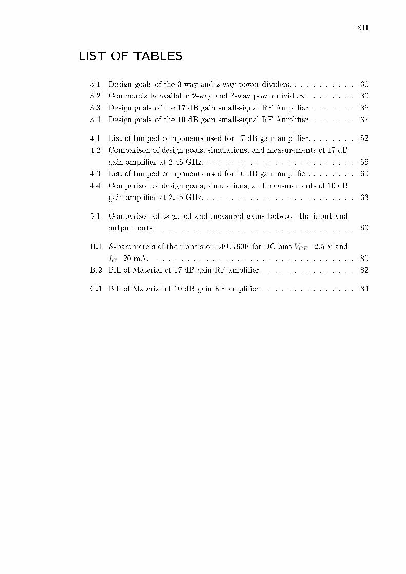
LIST OF TABLES
3.1 Design goals of the 3-way and 2-way power dividers. . . . . . . . . . . 30
3.2 Commercially available 2-way and 3-way power dividers. . . . . . . . 30
3.3 Design goals of the 17 dB gain small-signal RF Amplier. . . . . . . . 36
3.4 Design goals of the 10 dB gain small-signal RF Amplier. . . . . . . . 37
4.1 List of lumped components used for 17 dB gain amplier. . . . . . . . 52
4.2 Comparison of design goals, simulations, and measurements of 17 dB
gain amplier at 2.45 GHz. . . . . . . . . . . . . . . . . . . . . . . . . 55
4.3 List of lumped components used for 10 dB gain amplier. . . . . . . . 60
4.4 Comparison of design goals, simulations, and measurements of 10 dB
gain amplier at 2.45 GHz. . . . . . . . . . . . . . . . . . . . . . . . . 63
5.1 Comparison of targeted and measured gains between the input and
output ports. . . . . . . . . . . . . . . . . . . . . . . . . . . . . . . . 69
B.1 S -parameters of the transistor BFU760F for DC bias VCE=2.5 V and
IC=20 mA. . . . . . . . . . . . . . . . . . . . . . . . . . . . . . . . . 80
B.2 Bill of Material of 17 dB gain RF amplier. . . . . . . . . . . . . . . 82
C.1 Bill of Material of 10 dB gain RF amplier. . . . . . . . . . . . . . . 84
1
1. INTRODUCTION
Currently most of the engineering companies, for example, NXP Semiconductors,
Freescale Semiconductors, Inneon, are paying extra attention in developing new
devices or systems which are compatible with the industrial, scientic, and medical
(ISM) frequency band. This is due to fact that, the ISM band is an unlicensed
frequency band. Thus, it oers an attractive alternative over the high cost licensed
frequency spectrum. Today the most popular license free ISM band is 2.4 GHz band
and is available in many regions of the world. As a consequence the applications
at this frequency band are growing rapidly. The ISM 2.4 GHz frequency band
approximately ranges from 2.4 GHz to 2.5 GHz. In the electromagnetic frequency
spectrum the ISM frequency part is dened by the International Telecommunication
Radio Sector (ITU-R) on May, 1985. In addition to the microwave oven which
operates at 2.4 - 2.5 GHz frequency band approximately centered at 2.45 GHz, the
other communication devices those operating in this ISM band includes Wireless
Local Area Networks (WLANs) and Wireless Sensor Networks (WSNs), Bluetooth,
cordless phones, toys [1], [2], [3].
In the past the radio frequency (RF) energy (electromagnetic wave) was exten-
sively used for radio communication. In recent years, there has been a lot of inno-
vative research in RF energy which has brought tremendous advancements in the
application areas. The examples include, RF plasma lighting, automotive (RF spark
plugs), industrial, medical [4], [5]. One such exciting RF energy application and in-
spiration for this thesis work is the Solid State Cooking (SSC) technology. In this
technology the conventional magnetron tube in the microwave oven used for gener-
ating the microwave radiation is replaced with the high power solid state ampliers.
The operating frequency of the magnetron tube in most of the countries is 2.4 GHz
ISM band.
The conventional microwave oven uses the magnetron tube for generating mi-
crowave signals to cook/heat the food. These ovens are not capable of uniform
distribution of RF energy within the cavity. One reason for this is due to the fact
that the electromagnetic waves are not fully absorbed by the load (food) inside the
cavity, this is because of the properties of the load. The absorption of the elec-
tromagnetic waves depends on many factors for instance, quantity, placement, and
properties. The current microwave oven technology does not take into account the

1. INTRODUCTION 2
fact that the absorption of the RF energy depends on the load properties. The
second reason is the reection of the electromagnetic waves inside the cavity. When
the reected signals are combined with the incoming the electromagnetic signals,
then these signals have the property to either add or subtract with each other.
This results in either a very high or very low power at random places within the
cavity. This causes standing waves, which produces a non-uniform eld inside the
cavity. The current solution for this problem is the rotating plate. This exposes the
load to the maximums and minimums simultaneously also it protects the load from
overheating [6].
The SSC technology takes into to account the properties of the load and also
it takes advantages of these features. The properties of standing waves depend on
several factors. The three important factors of the incoming waves are amplitude,
frequency, and phase. By having more than one RF energy source (high power
amplier) and by varying their amplitudes, frequencies, and phases dierent wave
patterns can be generated within the cavity. With this solution the load absorbs the
RF energy from all sides. These high power ampliers are required to be provided
with an RF input signal at a required frequency and at a low power level for the
purpose of driving the high power ampliers. This is because the high power ampli-
ers can only amplify the RF input signal to a certain level. They are not capable
of generating the RF input signal on their own. This signal generation at low power
with a specic frequency is done by the Small-Signal Board (SSB). Figure 1.1 shows
the block diagram of the system.
Signal Generator
(Local Oscillator)
ApplicationØ
Phase Shifter Amplifier 1 Amplifier 2High Power
Amplifier
SSB
Figure 1.1. SSB and high power amplier setup description.
The signal generator is a local oscillator which generates the RF input signal
with a specic frequency. Then the signal goes through a phase change by the phase
shifter. The signal is then amplied by a couple of amplier stages before nally it
is fed to the high power amplier.
My role in this SSC project is to re-design the existing SSB. The re-designed
SSB should have the exibility to congure either in single channel or multi channel
master/slave conguration and simultaneously to achieve modularity. With this re-
designed SSB the application areas can be extended. In multichannel conguration
the SSB should have the possibility of using the RF input signal generated by on-
board local oscillator or RF input signal generated by the local oscillator on the other

1. INTRODUCTION 3
channel. In master conguration, the RF input signal generated by the on-board
local oscillator is distributed to the succeeding channels. On the other hand, in slave
conguration, the SSB gets the RF input signal from the preceding master/slave
channel; the on-board local oscillator is disabled with the software program in this
conguration. The re-designed SSB should also provide the local oscillator signal
as a reference signal for the control/monitoring purpose. This can be accomplished
with a power divider. The power divider should have two inputs and three outputs.
This thesis work presents the prototyping of this 2.4 GHz ISM band power divider.
The signal power loss during the division operation is made up with the small-signal
RF amplier. The power divider is realized by 3-and 2-way power dividers and two
small-signal RF ampliers. Both, power dividers and ampliers are designed and
developed as a standalone device and the prototyping of the ISM band power divider
is done by integration of all the fabricated devices on a single substrate.
1.1 Motivation
The aim of this thesis work is to prototype a low cost power divider which has two
inputs and three outputs which operate at ISM 2.4 GHz band. Numerous power
dividers are available in the market today but, less expensive, high performance,
reproducibility, and compact solution is the main motive. Furthermore, the pro-
totyped power divider is required to have the possibility of mass production with
minimum deviation in the performance parameters in the operating frequency band.
The small-signal ampliers has to be developed by the use of NXPs active devices
only. The more detailed design requirements are mentioned in Chapter 3.
1.2 Objectives and Scope of the Thesis
The objective behind this thesis work is to design and construct 3-and 2-way power
dividers and ampliers as a standalone devices and prototyping of ISM band power
divider by integration of dividers and ampliers. The scope of this thesis work is as
follows:
Literature review of the power dividers and small-signal RF ampliers.
Selection of suitable topology for the power divider realization.
Selection of suitable small-signal RF amplier design procedure.
Designing and simulations in Agilent Advanced Design System (ADS).
Fabrication and prototyping of both (dividers and ampliers) devices as a
standalone devices and performance measurements.
Prototyping of ISM 2.4 GHz power divider by integration of dividers and
ampliers on a single substrate.

1. INTRODUCTION 4
1.3 Thesis Outline
The whole thesis work is divided into 7 chapters. Chapter 1 is Introduction itself.
Besides the introduction, it also covers thesis objectives and outline.
Chapter 2 is Basics of Related RF Concepts. It provides the basics related to
elementary radio frequency design and performance parameters. These parameters
are proving important in RF design and characterization. The performance param-
eters of a two-port network such as scattering (S )-parameters and stability factors
are briefed. The impedance matching network design and selection of the DC bias
circuits are also described. Additionally, the power gain relations and gain circles
are also presented. Furthermore, linearity concepts are discussed at the end of this
chapter.
Chapter 3 is Theoretical Background and Design Goals. It elaborates the liter-
ature review of dierent power divider topologies and amplier design procedures.
The dierent power divider topologies are discussed along with their implementa-
tion, advantages, and disadvantages. Finally, the specications of the 3-and 2-way
power dividers are tabulated. Then it follows the RF amplier design procedures
from dierent authors. Next, it follows the specied gain amplier design proce-
dure. Finally, the design requirements of the ampliers which are used in realizing
the power divider along with its purpose are detailed.
Chapter 4 is Implementation all about the implementation of the power dividers
and small-signal RF ampliers. First, the 3-way power divider design process is
presented along with the simulation results, fabrication, and measurement results.
A photograph of the fabricated 3-way power divider is also presented. Next, the 2-
way power divider design ow is discussed in detail. Commercially available dividers
on the market are also presented. Next, the detailed design description of the small-
signal RF ampliers is described. It includes the selection of transistor and RF
design process. Along with this simulation results, layout and fabrication, and
measurement results are also presented.
Chapter 5 presents the Prototyping of the power divider by integration of 3-
and 2-way power dividers and two small-signal RF ampliers on a single PCB. The
simulation results of the power divider are given along with the layout. A photograph
of the prototyped power divider and its measurement results are presented.
Chapter 6 is Discussion about the simulations and measurement results. Both,
3-and 2-way power dividers and ampliers are discussed separately. Then, the pro-
totyped power divider results are discussed.
Finally, Chapter 7 is all about the Conclusion and also some recommendations
for the future work are suggested.

5
2. BASICS OF RELATED RF CONCEPTS
This chapter outlines the basics of RF concepts which are proving important in
RF amplier design. First, the Scattering parameters are presented with respect
to the two-port networks. The Scattering parameters are considered as important
parameters in the amplier design and characterization. After this the stability
issues and gain relations in the two-port networks are explained. Next, impedance
matching concepts and DC bias circuits will be discussed. Finally non-linearities in
ampliers are introduced in Section 2.6.
2.1 Scattering Parameters
Linear and non-linear networks are characterized by measuring the parameters at
the input and output terminals so called ports, by ignoring the actual contents
inside the network [7]. In this context the parameters are the voltages at nodes
and currents in branches. By applying simple open- and short-circuit conditions
at ports these parameters are measured practically. However, it is only possible
at low-frequencies [8]. This technique is not feasible at high frequencies. This is
because the voltages at nodes and currents in branches changes more rapidly at
higher frequencies. Therefore the measurement of voltages at nodes and currents in
branches at high frequencies are highly problematic. In addition, the magnitude of
the inductance of the wire can be signicantly high while implementing the short-
circuit condition. Also, the open-circuit condition can lead to capacitive loading.
Moreover, the open- and short-circuit conditions at high frequencies lead the active
device (transistor) to oscillate. In many cases these oscillations destroy the active
device [9].
In order to overcome these problems at microwave (MW) and radio frequencies
a new set of parameters called Scattering parameters or simply S -parameters are
introduced. With these parameters the networks are modeled in terms of incident,
reected, voltage or current waves [10]. S -parameters are specically used for small-
signal representation of the network [9]. And besides, these parameters are used in
modeling of passive and active components. The S -parameters are extensively used
in the microwave and radio frequency design and measurements. Furthermore, the
other parameters like, impedance (Z )-, admittance (Y )-, hybrid (H )-, and ABCD-
parameters can be derived from the S -parameters, the derivations are given in [8].

2. BASICS OF RELATED RF CONCEPTS 6
The S -parameter technique is a simple and yet most powerful tool used in RF
and microwave engineering stream. The advantages of S -parameters over the other
parameters are convenient to measure, easy to understand, and to work with at
high frequencies. Moreover, they are more accurately measured parameters at mi-
crowave frequencies. In addition, they provide in-depth understanding of a design
or measurement [7], [11]. The matrix representation of these parameters is called
S -matrix.
Let us consider an amplier as a two-port network, an input port, and an output
port, as depicted in Figure 2.1 and the S -parameters of this two-port network is
expressed in the following form [12] as
Active
Two-Port
Network
Port 1 Port 2
Input port Output port
V1+
V2
+
V1- V2
-
S11 S22
S21
S12
Figure 2.1. Two-port network S-parameters representation.
V −1 = S11V
+1 + S12V
+2 , (2.1)
V −2 = S21V
+1 + S22V
+2 , (2.2)
where V +1 , V −
1 are the incident wave and the reected wave voltages at port 1, V +2 ,
V −2 are the incident and reected wave voltages at port 2, and S11, S12, S21, and S22
are the S -parameters usually these are expressed in complex numbers. The S -matrix
is described as
S =
[S11 S12
S21 S22
]. (2.3)
It is important to note that the DC power supply port of the amplier is usually
ignored in this type of modeling. Meaning that, the S -parameters of an amplier
are given for a particular bias current. Besides that, the S -parameters are expressed
for a single frequency only. The matrix representation of equations (2.1) and (2.2)
are as follows [V −1
V −2
]=
[S11 S12
S21 S22
][V +1
V +2
]. (2.4)
Now, let us determine the S -parameters from equations (2.1) and (2.2). From
equation (2.1) the S11-parameter, the so called input reection coecient at port 1
2. BASICS OF RELATED RF CONCEPTS 7
is given by
S11 =V −1
V +1
∣∣∣∣V +2 =0
. (2.5)
The condition V +2 =0 in equation (2.5) means the wave entering at port 2 is zero.
In other words, the port 2 is terminated with a matched load; in this case it is 50 Ω.
Commonly, the majority of the radio frequency and microwave systems are designed
for 50 Ω impedance. From equation (2.2) the S21-parameter so called transmission
parameter or forward gain or simply the gain from port 1 to port 2 is given by
S21 =V −2
V +1
∣∣∣∣V +2 =0
. (2.6)
Next, the S22-parameter, the so called output reection coecient from the equa-
tion (2.2) is given by
S22 =V −2
V +2
∣∣∣∣V +1 =0
. (2.7)
The condition V +1 =0 in equation (2.7) means the wave entering at port 1 is zero.
Likewise, the S12-parameter, the so called reverse isolation or reverse gain from port
2 to port 1 from (2.1) is given by
S12 =V −1
V +2
∣∣∣∣V +1 =0
. (2.8)
In ampliers, the S21-parameter is usually expressed in decibels (dB), in logarith-
mic scale, commonly it is termed as gain. The Return Loss (RL) is a measure of how
close the input and output impedances of an amplier to the reference impedance,
in most cases 50 Ω. The input return loss of an amplier is expressed as
RLIN(dB) = 20 ∗ log10
∣∣∣∣ 1
S11
∣∣∣∣ , (2.9)
similarly, the output return loss as
RLOUT (dB) = 20 ∗ log10
∣∣∣∣ 1
S22
∣∣∣∣ . (2.10)
Return loss is dened as the ratio of the reected wave voltage to the incident
wave voltage expressed in dB. S -parameters are utilized in further sections while
dealing with the stability, power gains, and impedance matching networks.

2. BASICS OF RELATED RF CONCEPTS 8
2.2 Stability
Stability is an important parameter in the RF and MW amplier circuit design.
A typical amplier will not oscillate with any passive load or source terminations.
Stability is dened as the tendency of the amplier to not oscillate. In the majority
of the applications the stable performance of the amplier is necessary. Since, if the
amplier oscillates it consumes more current by changing the bias condition results
in an increase in power dissipation in the form of heat. Eventually it will damage
the active device in the circuit [13]. Furthermore, the amplitude of the oscillations
increases with time. When this signal level crosses the threshold level then the active
device forced into large signal operation. This can also cause damage to it or any
other connected device.
The presence of the feedback path in the circuits is one of the main reasons for the
oscillations. The feedback can be of two types: positive feedback and negative feed-
back. In a positive feedback system, the magnitude of the reected signal amplitude
level is higher than the forward signal amplitude level. This increase in amplitude
destroys the device by increasing the heat dissipation in the device itself. But, in
a negative feedback system the reected signal amplitude is lower than the forward
signal amplitude level. The reected signal will die out with the time. An amplier
may have the tendency to oscillate at any frequency ranging from the lower to higher
frequencies. In the majority of the applications the stable operation of the amplier
at all frequencies is preferred. In other words, in most applications stable operation
at the stop band frequencies is also important apart from the pass band frequencies.
This is because, the oscillations in the stop band frequencies may mix up with the
pass band frequencies and falls near to the pass band results in oscillations in the
frequency of interest.
Other reasons for oscillations in ampliers are due to uctuations in temperature,
bias currents, input signal level, the amplication of the device greater than unity,
external circuits connected to it and its parasitic, or device internal feedback. In
most cases, the last one is the main cause for any unwanted oscillations [14].
The stability of a two-port network can be described in two ways, unconditionally
stable or potentially unstable. If the two-port network is unconditionally stable then
it will not oscillate with any passive load or source terminations at all frequencies.
The potentially unstable two-port network is stable only for certain frequencies and
may have the tendency to oscillate for certain load or source terminations. In many
cases, the main goal of the designer is to achieve the unconditional stability. It may
be problematic for the designer to select the active device that is unconditionally
stable at all frequencies.Nevertheless, the unconditional stability can be achieved by
utilizing the stabilization techniques discussed in the following sections [15].

2. BASICS OF RELATED RF CONCEPTS 9
2.2.1 General Concept
Let us consider a two-port network that is connected to a generator at the one end
and termination at the other end as shown in Figure 2.2, along with the reection
coecients at the input and output ports.
Two-Port
Network
Zg
Eg ZL
+
-
ΓLΓs
Γin Γout
Figure 2.2. Two-port network reection coecients representation at every port alongwith source and load terminations.
Where ΓL and Γs are the load and source reection coecients, Γin and Γout
are the input and output reection coecients, Eg and Zg are the generator and
its impedance, and ZL is the load impedance with which the two-port network is
terminated.
If the absolute values of the input and output reection coecients are less than
one [15] then the two-port network is unconditionally stable. Meaning that, if |Γin|
<1, then the amplitude of the reected wave amplitude decreases (negative feedback)
eventually die out with the time. On the other hand, if |Γin|>1, then the amplitude of
the reected wave amplitude increases (positive feedback), which causes the active
device to oscillate. Therefore, the conditions for the unconditional stability are
identied as follows [8]
for
Γs < 1, (2.11)
and
ΓL < 1, (2.12)
|Γin| =∣∣∣∣S11 +
S12S21ΓL
1− S22ΓL
∣∣∣∣ < 1, (2.13)
|Γout| =∣∣∣∣S22 +
S12S21Γs
1− S11Γs
∣∣∣∣ < 1. (2.14)
From the equations (2.13) and (2.14) it can be observed that the two-port network
stability is dependent on ΓL, Γs, and S -parameters. Since the S -parameters are
dened for single frequency from Section 2.1), the parameters on which the stability
of the two-port network depends on are ΓL and Γs. Depending on the values of the
reection coecients (load and source) the stability of the two-port network can

2. BASICS OF RELATED RF CONCEPTS 10
be unconditionally stable or potentially unstable and is determined by the stability
factors as follows.
2.2.2 Stability Factors
The stability of the two-port network is determined by the following stability factors:
µ (Mu), µ′(Mu-prime), and Rollett stability factor k [15]. These are calculated with
the S -parameters. According to the Rollett stability criterion the two-port network
is unconditionally stable, if both
k =1− |S11|2 − |S22|2 + |∆|2
2|S12||S21|> 1, (2.15)
and
∆ = S11S22 − S12S21 < 1, (2.16)
are satised. In [14], [16] it is stated that, the other conditions which are used
to determine the stability are almost similar to the stability factors mentioned in
equations (2.15) and (2.16). The complete derivation of Rollett condition, k>1, is
given in [15].
The µ and µ′factors, the so called load stability factor and source stability factor
respectively are also used to determine the stability of the two-port network in
terms of the S -parameters. The conditions that are to be satised for unconditional
stability of the two-port network referred to µ is given by
µ =1− |S11|2
|S22 − S∗11(S11S22 − S12S21)|+ |S21S12|
> 1, (2.17)
and, regard to µ′is given by
µ′=
1− |S22|2
|S11 − S∗22(S11S22 − S12S21)|+ |S21S12|
> 1. (2.18)
Either of µ or µ′is enough to determine the stability of a two-port network.
Meaning that, a two-port network is unconditionally stable if µ>1 or µ′>1 [17]. If
µ and µ′are less than or equal to one (µ≤1 and µ
′≤1) then the two-port network
is potentially unstable.
2.2.3 Stability Circles
As mentioned in Section 2.2, if the two-port network is potentially unstable (µ≤1,µ
′≤1, |ΓL|>1, |Γs|>1) then it may oscillate for certain combinations of load and
source impedances. These impedances are determined with the help of the stability

2. BASICS OF RELATED RF CONCEPTS 11
circles by plotting on the Smith chart. The stability circle is the border line between
the source or load impedances for which they cause the two-port network to oscillate
and for which they do not [18].
From the equations (2.13) and (2.14) it can be observed that, Γin and Γout are
dependent on the load and source terminations that is, ΓL and Γs. First, let us
consider Γin. For certain load impedances ΓL can be greater than or less than unity.
Since, for unconditional stability at the source side, the chosen load impedances
should satisfy both Γin<1 and also ΓL<1 simultaneously. In the same way, Γout<1
and also Γs<1 for unconditional stability at the load side. The borderline between
the stable and unstable region at the load side can be interpreted by a circle called
the output stability circle (Figure 2.3 (a)) for all values of ΓL when |Γin|=1. The
center, CL, of the output stability circle is at
CL =(S22 − (S11S22 − S12S21)S
∗11)
∗
|S22|2 − |(S11S22 − S12S21)|2, (2.19)
and the radius, rL, of
rL =
∣∣∣∣ S12S21
|S22|2 − |(S11S22 − S12S21)|2
∣∣∣∣ . (2.20)
Similarly, at the input side the input stability circle (Figure 2.3 (b)) is used to
dierentiate the stable and unstable regions. The input stability circle is plotted for
Γs when |Γout|=1. The expressions for the center, CS, and radius, rS, of the input
stability circle are given in [15].
Furthermore, µ>1 and µ′>1 gives the minimum distance between the center of
the Smith chart and the unstable regions in ΓL and Γs plane.
CS
rS
µ'
Γs plane ΓL plane
|Γin|=1
|Γout|=1
CL
rL
µ
(a) (b)
Figure 2.3. Stability circles of a two-port network plotted on the Smith chart: (a) Outputstability circle on the ΓL plane center is at, CL, is a complex number. With a radius of rL,where µ is the minimum distance between the center of the Smith chart and the unstableregion, (b) Input stability circle on the Γs plane center is at, CS, is a complex number.With a radius of rS, where µ
′is the minimum distance between the center of the Smith
chart and the unstable region.

2. BASICS OF RELATED RF CONCEPTS 12
By considering the absolute values of the S11, S22, Γin, and Γout the stable and
unstable regions on the Smith chart can be predicted with respect to the stability
circles. If ΓL=0, Γs=0 and if |S11|<1, |S22|<1 then, |Γin|<1 and |Γout|<1 is true
therefore, the two-port network is stable. In this case, if the input and output
stability circles include the center of the Smith chart then the stable region is inside
the stability circle. If the center of the Smith is excluded then the outer region
of the stability circle is the stable region (Figure 2.4 (a) and (c)). Likewise, if
|S11|>1, |S22|>1 then, |Γin|>1 and |Γout|>1 is true therefore, the two-port network
is unstable. In this case, the region inside the stability circle is the unstable region
if it encloses the center of the Smith chart. If the stability circle excludes the center
of the Smith chart then the outer region of the stability circle is the unstable region
(Figure 2.4 (b) and (d)) [15].
CS
rS
µ'
Γs plane
|Γin|=1
|Γout|=1
CL
rL
µ
Stable region
Unstable region
|S11|<1
|Γin|<1
|Γin|=1
CL
rL
µ
|S11|>1
|Γin|>1
ΓL plane ΓL plane
|S22|<1
|Γout|<1
CS
rS
µ'
Γs plane
|Γout|=1
|S22|>1
|Γout|>1
(a) (b)
(d)(c)
Figure 2.4. Representation of the stable and unstable regions on the Smith chart withrespect to the stability circles: (a) Output stability circle with stable region outside thestability circle on ΓL plane, (b) Output stability circle with stable region inside the circleon ΓL plane, (c) Input stability circle with the stable region outside the stability circle onΓs plane, (d) Input stability circle with the stable region inside the circle on Γs plane.
A potentially unstable two-port network can be made unconditionally stable by
employing stabilization techniques. They are, inductive degeneration technique,
base and collector resistive (series or shunt) loading, or a feedback network. Usually
the resistive loading is implemented either in series, in shunt, or both at the output

2. BASICS OF RELATED RF CONCEPTS 13
with the cost of the degradation of the circuit performance, mainly gain. More
theoretical and mathematical information on stability is available in [13], [15], [17],
and [19].
2.3 Power Gain Relations and Gain Circles
Let us consider a two-port network connected to a generator and to a load termi-
nation as shown in Figure 2.5. Four powers which can be identied at every port
in that two-port network are: available power from the generator, Pavg, the input
power to the two-port network, Pin, available power from the two-port network,
Pavn, and power delivered to the load, PL [20].
Two-Port
Network
Zg
Eg ZL
+
-
PavgPavnPin
PL
Figure 2.5. Representation of powers at every port in a two-port network.
The power gains such as, available power gain, GA, transducer power gain, GT ,
and power gain, GP , are dened in terms of powers at every port and S -parameters as
follows. The transducer power gain, GT , is the actual gain of the two-port network
including the input and output matching networks (discussed in Section 2.4). In
terms of powers it is dened as the ratio of the power delivered to the load, PL, to
the available power from the generator, Pavg. This is expressed in the following form
as [21]
GT =PL
Pavg
=(1− |ΓL|2)|S21|2(1− |Γs|2)
|(1− S22ΓL)(1− S11Γs)− S12S21ΓLΓs|. (2.21)
GT is dependent on both Zg and ZL, and both are equal to the characteristic
impedance, Z0. The more simplied form of GT is obtained by substituting in
either of the equation (2.13) or equation (2.14) which also helps in deriving GA
and GP . For instance, by making the load reection coecient (ΓL) is equal to the
complex conjugate of the output reection coecient (Γ∗out), and by substituting it
in equation (2.21) yields available power gain GA. In powers, it is dened as the
ratio of available power from the network, Pavn, to the available power from the
generator, Pavg. The expression for GA is given as
GA =Pavn
Pavg
=1− |Γs|2
|1− S11Γs||S21|2
1
1− |Γout|2, (2.22)

2. BASICS OF RELATED RF CONCEPTS 14
GA depends only on Zg not on ZL.
Next, power gain GP is also known as operational power gain and is dened as
the ratio between the input power, Pin, and power delivered to the load, PL. It
depends only on ZL not on Zg. The expression for GP is given as [15]
GP =Pin
PL
=1
1− |Γin|2|S21|2
1− |ΓL|2
1− |S22ΓL|2. (2.23)
With the help of GA and GP the gain circles are described. The gain circles are
drawn on the Smith chart. In the amplier design, these gain circles are used to
locate the available gain and power gain. In addition to GA, GT , and GP , the other
gains such as, maximum available gain (MAG) and maximum stable gain (MSG)
are also commonly described. The MAG and MSG are generally used in the data
sheets to represent the maximum capabilities of the transistor [8]. The MAG is
dened as the maximum transducer gain. That is, it is the maximum gain possible
to achieve with the conjugate matching in a two-port network. The transistor should
be unconditionally stable (k>1) for calculating the MAG. The highest gain that is
possible to achieve from a potentially unstable two-port network after making it
stable is the MSG and is expressed in the following form:
MSG =|S21||S12|
. (2.24)
2.4 Impedance Matching Networks
In the high-frequency design, maximum transfer of power at every port is often an
important requirement with less possibility of reections and also with low signal
energy loss. This can be accomplished by a network called impedance matching
network which transforms the source impedance to the load impedance. A simple
two-port network with the impedance matching networks at the input and output
is shown in Figure 2.6. Generally, matching networks are deployed at the input and
output of an amplier.
Two-Port
Network ZL
Zg
Eg
+
-
Output
Matching
Network
Input
Matching
Network
Figure 2.6. Two-port network with the input and output matching networks.
The input impedance matching network transforms the two-port network input
impedance to the generator impedance, Zg. Thus, the maximum input signal power

2. BASICS OF RELATED RF CONCEPTS 15
is fed into the two-port network. Similarly, with the output matching network maxi-
mum power is delivered to the load from the two-port network output. Additionally,
it protects the two-port network from the reections caused by the impedance mis-
match resulting from the external circuits connected to it [18], [22].
The following attributes should be considered while designing the impedance
matching network [23]:
Complexity - It is always wise to choose a simple, with few possible components
as an impedance matching network with which the design specications can
be accomplished. The impedance matching network with fewer components
can be inexpensive, compact, and also will introduce less loss.
Bandwidth - There are numerous topologies are available to design a matching
network for the single frequency only. However, in many applications, a band of
frequencies needs to be matched to the load. In this situation, the complexity
of the matching network increases and also it can be less reliable.
Implementation - Based on the type of application, power level, frequency
of operation, and PCB area available, the matching networks are designed.
These matching networks can be composed of lumped components (resistors,
inductors, or capacitors), quarter-wave transformers, and stubs. In some cases,
their combinations are also preferred.
Adjustability - In some applications, an adjustable matching network needs
to be designed for various load impedances after the circuit is fabricated. In
these situations, inductors or capacitors can be used. Because, it is easier to
modify lumped components than stubs or quarter wave transformers, for that
matter.
Impedance matching can be accomplished either with stub (single stub or dou-
ble stub) or discrete components. The stub matching networks are more complex
compared to the other circuits. The discrete component impedance matching net-
works are more often preferred at radio frequencies. These are made up of resistive
elements, reactive elements or both. The rst mentioned one is not practically used
because it dissipates power and also introduces noise to the circuit. The reactive
elements (inductor or capacitor) impedance matching networks are the simplest and
most widely used matching networks. These are categorized into two types. The rst
type is a two element network, a so called L-network. The second type is a three-
element network. Eight possible combinations of L-network matching networks are
given in [8].

2. BASICS OF RELATED RF CONCEPTS 16
2.5 DC Bias Circuits
The main purpose of the DC bias circuit is to retain the DC operating point stable
against the temperature uctuations. The DC operating point is also known as
DC bias point or simply quiescent (Q) point. For instance, in bipolar junction
transistors (BJT) the DC current gain, hFE, and the base-to-emitter voltage, VBE,
are the parameters which are dependent on the variations in the temperature. A
raise in the temperature will result in decrease of a VBE at a rate of 2.5 mV/0C
and also increase of hFE at a rate of 0.5%/0C from its theoretical value at room
temperature [18]. Furthermore, hFE is also dependent on the process variations. It
is almost impossible to manufacture two identical devices with respect to hFE. Most
often this is the reason for wider specication of the DC current gain.
One solution to overcome these problems is by utilizing an active bias circuit.
More often it employs an IC or an extra active device (generally transistor), and
less resistors which keeps VBE and IC constant against variation in hFE and tem-
perature drifts. But, due to the cost considerations these circuits are generally not
preferred. However, the active bias circuits are widely used in applications where
higher temperature variations are expected. And also,in applications where cost is
not a big concern.
Unlike active bias circuits, the passive bias circuits are the most popular and most
widely preferred bias circuits even though these circuits oer stable DC bias point
operation over a moderate temperature variations. This is because, the passive bias
circuits are easy to implement and uses only a few resistors. Furthermore, these are
are easy to understand compared to the active bias circuits.
The simple non-stabilized BJT bias circuit which uses two resistors, base resistor,
RB, and collector resistor, RC , along with two DC supply voltages, VBB and VCC is
shown in Figure 2.7 [24]. The base current, IB, which ows into the transistor is set
by RB. The collector current, IC , is simply hFE times IB. The collector-to-emitter
voltage, VCE, is calculated by subtracting the collector voltage drop, VC , across RC
, from the supply voltage, VCC . If IC varies, VCE also varies depending on the
voltage drop across RC . The variation in IC due to process is directly proportional
to hFE for a xed VCC and VBE. Meaning that, for example, a 5% increase in hFE
will causes a 5% increase in IC . Hence, the non-stabilized BJT bias circuits do not
compensate the variations in hFE. However, VBB and VCC bias conditions can be
varied for compensating hFE variations.

2. BASICS OF RELATED RF CONCEPTS 17
VBB VCC
RCRB
Figure 2.7. Non-stabilized passive BJT bias circuit.
The voltage feedback BJT bias circuit (Figure 2.8 (a)) decreases the variations in
IC , which occurs due to variations in hFE. This is accomplished with the collector
to base feedback resistor, RB. The base current, IB, is derived from VCE which is
opposed by VCC . An increase in IC due to variations in hFE increases the voltage
drop across RC . This in turn decreases the collector-to-emitter voltage, VCE, which
causes the IB to decrease, then IC . In simple words, voltage feedback bias circuit
reduces the quantity that the collector current increased due to hFE. Meaning
that, the base resistor forms the negative feedback. In addition, it is the most
widely used inexpensive, simple DC bias circuit in radio frequencies. The emitter
terminal is directly connected to the ground. Thus very low emitter lead inductance
is possible. The voltage feedback with current source BJT bias circuit (Figure 2.8
(b)) is particularly used when VCC and VCE are greater than 15 V and 12 V. The bias
circuit shown in Figure 2.8 (c) is often employed in power ampliers. The emitter
feed BJT bias circuit (Figure 2.8 (d)) is usually used at low frequencies. Because,
at high frequencies the emitter resistor RE provides high AC gain loss [24].

2. BASICS OF RELATED RF CONCEPTS 18
VCC
RCRB1
RB
RB2
VCC
RCRB1
RB2
RC
VCC
RB1
RB2 RE
(a) (b)
(c) (d)
VCC
RCRB
Figure 2.8. Passive BJT bias circuits [24]: (a) Voltage feedback, (b) Voltage feedbackwith a current source, (c) Voltage feedback with a voltage source, (d) Emitter feedback.
2.6 Non-linearities in Ampliers
An amplier whose output response is a non-linear function of the input signal is
said to be a non-linear amplier. If the amplitude of the input signal exceeds a
certain limit then the output response may not be in linear relation to the input
signal. Since, the amplier is pushed into saturation. This results in dierent types
of distortions are as follows [13], [25]:
Frequency Distortion - is exhibited if the active components in an amplier
amplies certain frequency amplitudes dierently than the other frequencies.
This type of distortion is more often observed in situations where the amplier
is pushed to operate at its extreme limits.
Amplitude Distortion - is also known as non-linear distortion. If the amplier
is not properly biased then the transistor is pushed into either saturation or
cut-o region. This results in amplitude distortion.
Harmonic Distortion - by the application of the sinusoidal signal as an input
2. BASICS OF RELATED RF CONCEPTS 19
to a non-linear circuit, for instance amplier, the output spectrum can have
frequency components which are integer multiples of the input signal. This
type of distortion is known as harmonic distortion.
Gain Compression - means decreasing the gain of an amplier with an increase
in amplitude of the input signal. It is due to the operation of the transistor in
saturation.
Cross Modulation - this phenomenon occurs when a weak desired signal and
a strong interfering signal passes through a non-linear (amplier) circuit. The
modulation is shifted from the strong interfering signal to the weak desired
signal. Generally, this is noticed in ampliers when the amplier amplies
signals from dierent channels at the same time. For example, in television
transmitters.
Intermodulation Distortion - when the input signal consists of two or more
interference signals which are closely spaced with respect to the main signal
frequency then the non-linear system produces intermodulation components
which interfere with the desired signal. In this situation, the output spectrum
exhibit components that are not harmonics of the input signals. This is due
to the mixing (multiplication) of the two frequencies.
In this work, our main focus is only on gain compression and intermodulation
distortion.
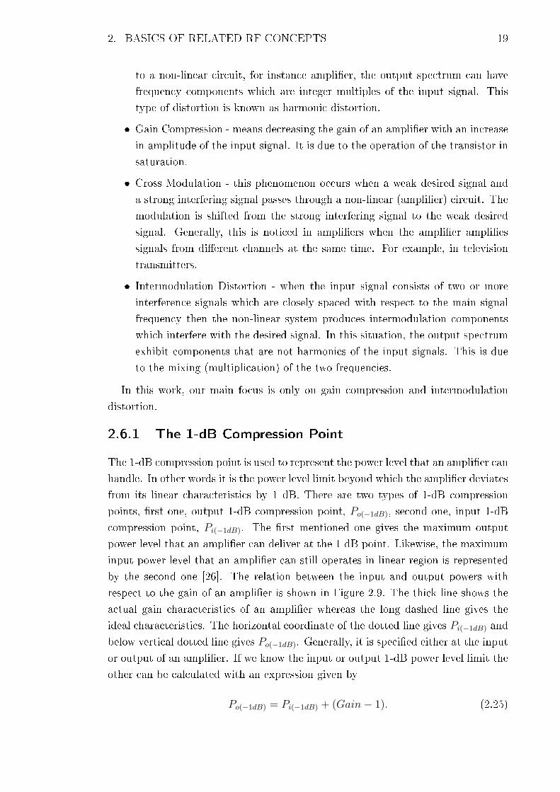
2.6.1 The 1-dB Compression Point
The 1-dB compression point is used to represent the power level that an amplier can
handle. In other words it is the power level limit beyond which the amplier deviates
from its linear characteristics by 1 dB. There are two types of 1-dB compression
points, rst one, output 1-dB compression point, Po(−1dB), second one, input 1-dB
compression point, Pi(−1dB). The rst mentioned one gives the maximum output
power level that an amplier can deliver at the 1 dB point. Likewise, the maximum
input power level that an amplier can still operates in linear region is represented
by the second one [26]. The relation between the input and output powers with
respect to the gain of an amplier is shown in Figure 2.9. The thick line shows the
actual gain characteristics of an amplier whereas the long dashed line gives the
ideal characteristics. The horizontal coordinate of the dotted line gives Pi(−1dB) and
below vertical dotted line gives Po(−1dB). Generally, it is specied either at the input
or output of an amplier. If we know the input or output 1-dB power level limit the
other can be calculated with an expression given by
Po(−1dB) = Pi(−1dB) + (Gain− 1). (2.25)
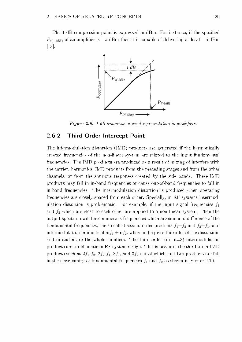
2. BASICS OF RELATED RF CONCEPTS 20
The 1-dB compression point is expressed in dBm. For instance, if the specied
Po(−1dB) of an amplier is +5 dBm then it is capable of delivering at least +5 dBm
[13].
PIN(dBm)
PO
UT
(dB
m)
Pi(-1dB)
Po(-1dB)
1 dB
Figure 2.9. 1-dB compression point representation in ampliers.
2.6.2 Third Order Intercept Point
The intermodulation distortion (IMD) products are generated if the harmonically
created frequencies of the non-linear system are related to the input fundamental
frequencies. The IMD products are produced as a result of mixing of interfere with
the carrier, harmonics, IMD products from the preceding stages and from the other
channels, or from the spurious responses created by the side bands. These IMD
products may fall in in-band frequencies or cause out-of-band frequencies to fall in
in-band frequencies. The intermodulation distortion is produced when operating
frequencies are closely spaced from each other. Specially, in RF systems intermod-
ulation distortion is problematic. For example, if the input signal frequencies f1
and f2 which are close to each other are applied to a non-linear system. Then the
output spectrum will have numerous frequencies which are sum and dierence of the
fundamental frequencies, the so called second order products f1+f2 and f2+f1, and
intermodulation products of mf1 ± nf2, where m+n gives the order of the distortion,
and m and n are the whole numbers. The third-order (m+n=3) intermodulation
products are problematic in RF system design. This is because, the third-order IMD
products such as 2f1-f2, 2f2-f1, 3f1, and 3f2 out of which rst two products are fall
in the close vanity of fundamental frequencies f1 and f2 as shown in Figure 2.10.

2. BASICS OF RELATED RF CONCEPTS 21
f1 f2
Frequency (Hz)
PIN
(dB
m)
f1 f2
Frequency (Hz)
PO
UT
(dB
m)
IMD
2nd order
products3rd order
products5th order
products
Fundamental
f2 -f1 2f1 -f2 2f2-f1 3f1 -2f2 3f2 -f1 f1+f2
Figure 2.10. Representation of intermodulation products produced in ampliers due tonon-linearities [27].
Filtering out of 2f1-f2 and 2f2-f1 products are considerably dicult since they
are very close to the pass band frequencies. The intermodulation distortion is the
dierence between the fundamental frequency power level and third-order intermod-
ulation products power (Figure 2.10).
The intermodulation products in an amplier are expressed in the gure of merit
and is called third-order intercept point (TOIP or IP3). The IP3 is measured with
a tow-tone test. In 2f1-f2, 2f2-f1, 3f1, and 3f2, the rst two products are two-tone
third-order intermodulation products. Since, they are generated by applying two-
tones at the input simultaneously. The two-tone output third-order intercept point,
OIP3, is calculated with the help of following expression
OIP3 = Pout +∆
2, (2.26)
where, Pout is the output power of the each tone in dBm, Pint is the intermodulation
power in dBm and ∆=Pout-Pint in dB as shown in Figure 2.11.
Frequency (Hz)
PO
UT
(dB
m)
f1 f2 2f1 -f2 2f2-f1
Pout
Pint
Figure 2.11. Third-order intermodulation products in ampliers.
Furthermore, two-tone input third-order intercept point, IIP3, is calculated from
the OIP3 and gain as
IIP3 = OIP3−Gain, (2.27)
The third-order intermodulation products power level increase/decrease by 3 dB
for every 1 dB increase/decrease in input fundamental signal power [27]. Meaning,

2. BASICS OF RELATED RF CONCEPTS 22
with increase in input signal level the intermodulation products increases rapidly
as shown in Figure 2.12. The thick line is the actual response of the amplier and
thick dashed line is third order intermodulation products. The intersection of these
lines is the IP3. Additionally, the horizontal coordinate of IP3 is denoted as IIP3
and vertical coordinate as OIP3. OIP3 is more commonly used in ampliers. More
detailed information on non-linearity in ampliers is reported in [13], [27], [28].
PIN(dBm)
PO
UT
(dB
m)
3
1 1
1
IP3OIP3
IIP3
Fundamental
3rd Order
Intermodulation
Products
Figure 2.12. Representation of OIP3 and IIP3 in ampliers.

23
3. THEORETICAL BACKGROUND AND
DESIGN GOALS
This chapter is mainly divided into two sections. The rst, section provides a brief
overview of power dividers. The various types of resistive power dividers along with
the schematics are presented. Then the design goals of the power dividers are listed.
The second section is all about the literature review of the RF ampliers, possible
amplier congurations, and amplier design procedures. It starts with the small-
signal RF ampliers introduction. Next, amplier congurations then the design
procedure of the RF ampliers from ve dierent authors are presented. Then the
specied gain amplier design procedure is also described. In Section 3.4 and 3.5
the design goals of the 17 dB and 10 dB gain small-signal RF ampliers are listed
respectively.
3.1 Power Dividers
In many radio frequency and microwave applications it is necessary to distribute the
power among various paths simultaneously. And also in some applications it is nec-
essary to provide the power to various lines from the same source. A simple possible
way this can be accomplished is with a device called power divider/splitter. The
resistor conguration used to separate the power is the basic dierence between the
power divider and power splitter [29]. Both, power dividers and power splitters, can
be realized either with transformers, lumped elements, quarter wave transformers,
micro-strip lines or strip lines.
A simple power divider which employs lumped component three-resistors and
power splitter with two-resistors are shown in Figure 3.1 [30]. It is important to note
that power dividers and power splitters are not interchangeable. Power dividers are
symmetrical and bidirectional devices. Meaning that, apart from the power division
power dividers can also be used in power combining applications. Like, in commu-
nication receivers where power from dierent sources are to be combined and also in
power ampliers to combine the power from dierent power ampliers. The other
applications of power dividers include, providing a sample signal for synchroniza-
tion or for monitoring purpose, in test systems to measure the frequency, power and
phase, for feedback, and in IMD measurements.

3. THEORETICAL BACKGROUND AND DESIGN GOALS 24
Z0/3
Port 2 (Output)
Port 3 (Output)
Port 1 (Input)
Z0/3
Z0/3
Port 2 (Output)
Port 3 (Output)
Port 1 (Input)
Z0
Z0
(a) (b)
Figure 3.1. Power divider and power splitter [30]: (a) Three-resistor power divider, (b)Two-resistor power splitter.
The block diagram of a three-port network, one input port and two output ports,
that is used as a power divider and a combiner is shown in Figure 3.2. As a power
divider, it takes input power, P1, and provides two output powers, P2 and P3, with
an attenuation of α dB. The power combiner performs the opposite action as that of
power divider. That is, it takes two powers as input powers, P1 and P2 and provides
its sum, P3, (P3=P1+P2) at the output port.
Power
Divider
Power
Combiner
P1
P2
P3=P1+P2
P3=αP1
P2=αP1 P1
(a) (b)
Figure 3.2. Power divider and power combiner [23]: (a) Power Divider, (b) PowerCombiner.
The power dividers are either three-port, or four-port, or more port devices. And,
also they can be either lossless or lossy. A basic three-port power divider provides
equal split (3 dB) of power among the two output ports. It is also possible to have
an unequal power divider. The typical specications of the power divider that are
to be achieved with the design based on the application are low insertion loss, good
return loss, high isolation, higher bandwidth, and small size [9].
If we consider a basic T-junction transmission line (three-port) lossless power
divider as shown in Figure 3.3 that has one input port and two output ports.
Port 1
Port 2
Port 3
Z0
Z 0
Z0
Figure 3.3. T-junction loss less power divider.
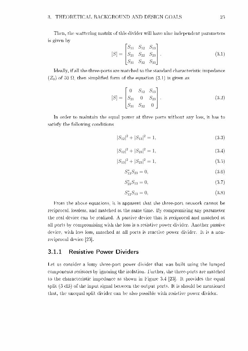
3. THEORETICAL BACKGROUND AND DESIGN GOALS 25
Then, the scattering matrix of this divider will have nine independent parameters
is given by
[S] =
S11 S12 S13
S21 S22 S23
S31 S32 S33
. (3.1)
Ideally, if all the three-ports are matched to the standard characteristic impedance
(Z0) of 50 Ω, then simplied form of the equation (3.1) is given as
[S] =
0 S12 S13
S21 0 S23
S31 S32 0
. (3.2)
In order to maintain the equal power at three ports without any loss, it has to
satisfy the following conditions
|S12|2 + |S13|2 = 1, (3.3)
|S12|2 + |S23|2 = 1, (3.4)
|S13|2 + |S23|2 = 1, (3.5)
S∗13S23 = 0, (3.6)
S∗23S13 = 0, (3.7)
S∗12S13 = 0, (3.8)
From the above equations, it is apparent that the three-port network cannot be
reciprocal, lossless, and matched at the same time. By compromising any parameter
the real device can be realized. A passive device that is reciprocal and matched at
all ports by compromising with the loss is a resistive power divider. Another passive
device, with less loss, matched at all ports is reactive power divider. It is a non-
reciprocal device [23].
3.1.1 Resistive Power Dividers
Let us consider a lossy three-port power divider that was built using the lumped
components resistors by ignoring the isolation. Further, the three-ports are matched
to the characteristic impedance as shown in Figure 3.4 [23]. It provides the equal
split (3 dB) of the input signal between the output ports. It is should be mentioned
that, the unequal split divider can be also possible with resistive power divider.

3. THEORETICAL BACKGROUND AND DESIGN GOALS 26
+-
+-
+ -
+-
V1
V 2
V
Z0
Z0
Z 0
Z
V3
Z0/3
Z 0/3
Z0 /3
A B
C
D
P1
P 2
P3
Zin
Port 1
Port 2
Port 3
Figure 3.4. Three-port equal split resistive power divider [23].
If we assume that all the three ports are terminated with Z0, then the impedance,
Z, seen by looking at P2 and P3 through Z0/3 resistor is given by
Z =
(Z0
3
) ∣∣∣∣∣∣∣∣ (Z0
3+ Z0 =
2Z0
3
). (3.9)
Then, the input impedance, Zin, seen at the input of the power divider is given
by
Zin =Z0
3+ Z. (3.10)
By substituting equation (3.9) in equation (3.10) results in
Zin =Z0
3+
2Z0
3= Z0. (3.11)
Thus, the input port is matched to Z0. It is due to the reason that, all the
three-ports are symmetrical and also matched. Means, S11=S22=S33=0.
The voltage, V , at node B is given by
V = V1 ×2Z0/3
Z0/3 + 2Z0/3=
2
3V1. (3.12)
Then, the voltages at nodes C and D are equal and is given by
V2 = V3 = V × Z0
Z0 + Z0/3=
3
4V. (3.13)

3. THEORETICAL BACKGROUND AND DESIGN GOALS 27
By substituting equation (3.12) in equation (3.13) results in the following expres-
sion
V2 = V3 =1
2V1. (3.14)
Thus, S21=S31=S23= -6 dB, meaning that the output power level at port 2 and
port 3 is 6 dB below the input power level at port 1.
Two possible topologies of the resistive power dividers are as follows [31], [32]:
Delta resistive power divider - in this topology the resistors are arranged in a
delta (∆) fashion as shown in Figure 3.5 a three port equal-split delta resistive
power divider. The drawback of this type of power dividers is that if the
number of output ports increases then the complexity of the divider increases.
Additionally, the calculation of resistor value becomes complex.
Z0
Z0
Z0
Port 3 (Output)
Port 2 (Output)
Port 1 (Input)
Figure 3.5. Equal-split delta resistive power divider.
T-junction resistive power divider - the conguration of the resistors in this
topology resembles the letter T. It is also called a Y resistive power divider.
It is the most preferred topology for the resistive power dividers. Because of
its advantages which includes, less complex, simple to understand, easier to
calculate resistor values, and the resistor values are lower than that of delta
topology (Figure 3.1 (a)).
The calculation of the resistor values in an arbitrary output port T-junction
resistive power divider are as follows:
All the resistor values in the resistive power divider are same. The resistor value
of an N-way T-junction resistive power divider is calculated with the help of the
following formula
R = Z0 ×(N − 1
N + 1
), (3.15)
where, Z0 is the characteristic impedance, R is the resistor, and N is the number of
output ports.
The insertion loss in dB is calculated with the formula as given below,
InsertionLoss = 10 ∗ log10((1/N)2)dB. (3.16)
For instance, a four-port power divider is termed as 3-way (three output ports)
power divider. It is a four-port device out of which one is the input port and the

3. THEORETICAL BACKGROUND AND DESIGN GOALS 28
remaining three ports are output ports.
3.1.2 Reactive Power Dividers
Reactive power dividers are the dividers those have isolation between the ports and
all the port are matched simultaneously. An example of a reactive power divider is
the Wilkinson power divider, which is realized with the micro-strip lines as shown
in Figure 3.6.
Z0
Z0
Z0
Z0√2
λ/4
Z 0√2
λ/4
2Z0Port 1
Port 2
Port 3
Figure 3.6. Three-port equal-split Wilkinson power divider [23].
In this work we will continue with the resistive power dividers only because of its
advantages such as, they are compact, realized with lumped components, extremely
broad band of operation, and are the only power dividers that can operate from DC
onwards, and more importantly suitable for mass production. More detailed infor-
mation on reactive power dividers can be found in [25] and [33]. A brief evaluation
of power dividers is presented in [34].
3.2 3-and 2-way Power Dividers Design Goals
The 3-way power divider port 1 is connected to the output of the signal generator
(local oscillator). The second port (port 2) is an auxiliary input. Port 3 is an
auxiliary output and port 4 is directly connected to the phase shifter input (Figure
3.7). When the system is congured as a single channel system the auxiliary input
and auxiliary output are terminated and the RF input signal from the local oscillator
is selected as source for the phase shifter. In a multi channel master conguration
the auxiliary input is terminated and the RF input signal is divided over the phase
shifter and the auxiliary output port.
In multichannel slave conguration, the on-board local oscillator is turned o and
acts as a 50 Ω termination. The RF input signal from the auxiliary input (connected
to the auxiliary output of the previous channel which provides the RF input signal)
will be divided among the phase shifter and auxiliary output. In a multi channel
conguration the auxiliary input will be connected to the auxiliary output of either
the master or the preceding slave small-signal board in a daisy chain system.

3. THEORETICAL BACKGROUND AND DESIGN GOALS 29
Port 1
Port 2
Port 3
Port 4
Auxiliary input
Auxiliary output
To phase
shifter inputSignal generator (local
oscillator) outputR1
R3
R4
R2
Figure 3.7. 3-way power divider showing the input and output ports purpose.
For monitoring purposes we require a second output of the selected source. In a
single channel or master conguration this would be the RF input signal from the
local oscillator. In a slave conguration the selected source would be the auxiliary
input of the 3-way power divider. This can be implemented with a 2-way power
divider, where the input port is connected to the auxiliary output of the 3-way
power divider. Port 2 of the 2-way power divider will then provide an output for
the monitoring purposes and port 3 will be the RF input signal for the following
channels (Figure 3.8).
Port 1
Port 3
Output for
monitoring purposeInput
Port 2
To next channel
auxiliary input
R1 R2
R3
Figure 3.8. 2-way power divider showing the input and output ports purpose.
The frequency of operation is ISM band, from 2.4 - 2.5 GHz centered at 2.45
GHz. The power dividers which are to be prototyped will be part of this thesis
work. The design goals of 3-way and 2-way power dividers are shown in Table 3.1.
Commercially available 2-way and 3-way resistive power dividers specications are
presented in Table 3.2. The insertion loss of 2-way resistive power divider presented
in [35] is 6.5 dB and 3-way divider in [37] is 9.5 dB.
3.3 Small-Signal RF Ampliers
An amplier is an active device that is designed to performs the amplication of the
voltage, current or both. Based on the frequency of the operation, the ampliers are
categorized. They are DC ampliers which operate at zero frequency, low frequency
ampliers (audio), and high frequency (RF) ampliers. Low frequency and high

3. THEORETICAL BACKGROUND AND DESIGN GOALS 30
Table 3.1. Design goals of the 3-way and 2-way power dividers.
Parameter3-way 2-way
UnitMin. Typ. Max. Min. Typ. Max.
Frequency 2.45 2.45 GHzReturn Loss 15 15 dBInsertion Loss 9.5 6.0 dB
Table 3.2. Commercially available 2-way and 3-way power dividers.
Source Parameter Range Unit
[35]Frequency DC-4 GHz
Insertion Loss 6.5 dB
[36]Frequency DC-18 GHz
Insertion Loss 6 dB
[37]Frequency DC-4 GHz
Insertion Loss 9.5 dB
frequency ampliers are also termed as AC ampliers. In AC ampliers, the small
amplitude input signal controls the large DC bias current. The typical performance
parameters which describe the amplier's performance are: power gain, input and
output return loss, gain compression, bandwidth of operation, power consumption,
and linearity [13].
RF ampliers are roughly classied into two categories: linear and non-linear
ampliers. If there is a xed ratio between the input and output at any time then
the amplier is said to be linear amplier. If the ratio is not xed, the amplier
is considered as non-linear amplier. In other words, the amplier, which preserve
the shape of the input signal at the output is called linear amplier. The ampliers
which can be modeled with linear S -parameters when the input signal amplitude is
small and the output signal amplitude varies in proportion to the input are small-
signal ampliers [38]. The linear ampliers operates with small-signals. The factors
which could possibly alter the ratio are the input signal power, frequency, biasing
conditions. Depending on the conguration, linearity, and eciency small-signal RF
ampliers are subdivided into dierent classes of ampliers, for example, class A,
class B, and class AB. Out of which class A ampliers are the more linear ampliers,
disadvantages of these are, that they are on contrast these are that they are the least
ecient amplier class.
3.3.1 Amplier Congurations
There are multiple amplier congurations where each one has its own advantages
and disadvantages. Depending on whether the base, emitter or collector terminal is
connected to the ground of an amplier three congurations are possible. They are

3. THEORETICAL BACKGROUND AND DESIGN GOALS 31
common-base (CB), common-collector (CC), and common-emitter (CE) congura-
tions. In the rst one, the input signal is injected between the emitter and ground
and amplied version of the input signal is provided between the collector and base
terminals. It is widely preferred conguration in realizing the high power and volt-
age ampliers. In the CC conguration, the input signal that is to be amplied is
applied between the base and collector terminal and the output is provided between
the emitter and collector terminals. The CC conguration has high input and low
output impedance. It is commonly used for current amplication applications and
least preferred for voltage amplications. More often it is used as buer amplier
or as an active impedance transformation circuit.
Finally, CE conguration (Figure 3.9) employs the input signal is fed into the
base, and the output connected at the collector. It is the most frequently used
conguration in almost all electronic circuits. Unlike, the other two congurations,
the CE conguration provides both current and voltage amplication and this makes
it the rst choice in power amplication applications. It is commonly used at radio
frequencies [13].
VCC
RC
RB
C
E
B
C1
C2
Output
Input
Figure 3.9. Common-emitter amplier conguration.
3.3.2 RF Amplier Design Methods
Design and development of an RF amplier for a particular application requires the
designer to follow certain steps or procedures. The basic steps that are followed in
almost all design processes are selection of a particular transistor, DC bias point
selection, stabilization, and the input and output matching networks. Still, the
designer has the choice to assign the priority to the steps. There are numerous
textbooks and publications are available today those describes the detailed step-by-
step design procedure of the RF amplier. The design procedures described in ve
dierent books are summarized below.
3. THEORETICAL BACKGROUND AND DESIGN GOALS 32
In [15] the author Gonzalez describes that a microwave amplier design is a pro-
cedure that is dependent on certain design goals and S -parameters of the transistor.
In the author's perspective, the design starts with a set of specications and the se-
lection of the transistor. Then it follows the unconditional stabilization of the tran-
sistor by utilizing the mathematical calculations and graphical techniques. Further,
it follows nding the suitable matching networks according to design requirements.
And, also the author claims that the DC bias circuit is the least considered one in
microwave amplier design. Nevertheless, the author expresses that the designer
should not compromise the amplier's performance by selecting a poor DC bias
circuit. The theoretical concepts required during development of radio frequency
ampliers are outlined in detail in [15] along with example designs.
A step-by-step design procedure of a class A amplier is presented in [13] by the
author Syre. The vital steps are described as follows:
Selection of suitable transistor based on performance parameters such as, fre-
quency, gain, and availability of the S -parameters les for DC bias currents,
and cost.
Selection of the right bias point by studying the transistor data sheet with
which the performance characteristics can be achieved.
Transistor stability check by inserting the S -parameters model from low to
high frequencies from the S -parameter le.
Making the amplier unconditionally stable with the necessary steps by check-
ing the stability factor k.
Designing of the input and output matching networks according to the design
requirements.
Adding the lumped and distributed component models and the substrate prop-
erties.
A three step procedure of an amplier design described by Vendelin [32] is as
follows:
1. DC Design.
2. RF Design.
3. Schematic and Layout design.
The author's prime focus is on the selection of the proper DC bias point and
bias circuit design. Furthermore, the author describes the relationship between the
DC bias current and the RF design. In addition, the author recommends using a
curve tracer in the DC bias circuit design. Three dierent biasing networks, such as,
3. THEORETICAL BACKGROUND AND DESIGN GOALS 33
four resistors, active bias, and active bias with diode are explained in [32]. Further,
the author compares the performance of these three bias circuits with respect to
the temperature and also performance enhancements. The design of a single stage
amplier for dierent requirements like, high-gain, maximum available gain, and
unilateral gain design is also presented.
Chang presented the step-by-step design procedure of a small-signal amplier. It
is given in [39]. Out of which, the essential steps are described below:
Tabulate the list of performance requirements. For instance, frequency band
of operation, power gain, return loss, OIP3.
Selection of an active device that suit best for the application.
Obtain the S -parameters from the vendor or by performing measurements.
Analyze the minimums and maximums of the active device performance pa-
rameters.
Perform the stability check and make it stable with the necessary steps if it is
unstable.
Examine constant gain circles on the Smith chart.
Compute maximum or desired power gain of the amplier.
Design the input and output matching networks to meet the performance
requirements.
The last author Bowick [18] claims that the DC bias circuit should be given
the highest priority. Dierent possible passive DC bias circuits are explained in
this book along with the examples. The design of a RF small signal ampliers with
both S - and Y -parameters are also presented. Further, the design of an amplier for
dierent goals such as, maximum gain or specied gain is also described. The design
method of a simultaneous conjugate match and a specied gain is also described.
All the procedures are presented with suitable design examples. This could serve as
a good reference for the RF amplier design.
Almost all of the above authors follow the similar procedure in stabilization and
power gain estimations, but, with dierent priorities with respect to the bias cir-
cuits, lumped components, and layout constraints. For instance, in [13] the author's
emphasizes on the inclusion of the resistive lumped components and the substrate
properties in order to achieve the real performance parameters. Further, in [32] the
author, Vendelin pays attention to the layout design as a part of the design proce-
dure. Vendelin and Bowick in contrast to Gonzalez give higher priority to the DC
bias circuit.

3. THEORETICAL BACKGROUND AND DESIGN GOALS 34
In this thesis work our goal is to design a small-signal RF amplier for a specied
gain. Therefore we discuss in more detail the specied gain design procedure in the
following section.
3.3.3 RF Amplier Design for a Specied Gain
In some applications the gain of the amplier should be less than the maximum
possible gain for that particular transistor in order to have a wide band of operation
and/or to provide an exact required specied gain without distortion. This can be
achieved with the input and output matching network design. Meaning that, by
introducing mismatch on purpose the gain is reduced to the desired gain. This is
termed as selective-mismatching [18], [23].
It is accomplished by plotting the constant-gain circles on the Smith chart to
represent Γs and ΓL which gives a constant source gain, GS, and load gain, GL.
For simplicity let us consider a unilateral device which means |S12|=0. Detailed
description for bilateral case is in [23], [32]. Then the expression for GS and GL can
be described as
GS =1− |Γs|2
|1− S11Γs|2, (3.17)
GL =1− |ΓL|2
|1− S22ΓL|2. (3.18)
If, Γs=S∗11 and ΓL=S
∗22 then maximum values of equations (3.17) and (3.18) are
given by
GSmax =1
1− |S11|2, (3.19)
GLmax =1
1− |S22|2. (3.20)
With the simplication procedure given in [22], the center and radius of the source
or input constant gain circle is given by
Cs =gsS
∗11
1− (1− gs)|S11|2, (3.21)
Rs =
√1− gs(1− |S11|2)
1− (1− gs)|S11|2. (3.22)
Similarly, the center and radius of the output is given by
CL =gLS
∗22
1− (1− gL)|S22|2, (3.23)
RL =
√1− gL(1− |S22|2)
1− (1− gL)|S22|2, (3.24)

3. THEORETICAL BACKGROUND AND DESIGN GOALS 35
where, gs and gL are the normalized source and load factor given in [23].
The center of the each circle (input and output) lies on the line given by the angle
of S∗11 and S
∗22. The values of Γs and ΓL are selected along these circles. There can
be many possible values for Γs and ΓL. With values selected closer to the Smith
chart center, the mismatch can be reduced and also the bandwidth can be improved
(see Section 2.2).
3.4 17 dB Gain Small-Signal RF Amplier Design Goals
The small-signal RF amplier developed in this thesis work is used for the re-design
of the SSB. This small-signal RF amplier is used to compensate the loss introduced
by both the 3-and 2-way power dividers, and the cable loss in case of a multi chan-
nel conguration (about 1 dB). The minimum loss introduced by the 3-way power
divider is roughly 9.5 dB and for the 2-way power divider is 6 dB. The total loss
would be 15.5 dB. By taking the cable and connector loss of approximately 1 dB (in
a multi channel conguration) into consideration, the total loss would be roughly
17 dB. So, in order to recover the signal loss of 17 dB, the gain of the amplier is
targeted to be 17 dB.
In this application, the required power at the output of the 2-way power divider
is 5 dBm [6]. Instead of compensating loss at every output port we decided to make
up the loss before the power is even inserted into the 2-way power divider. This way
we can compensate the loss of the two ports with only one amplier. Therefore the
desired input signal which is specied at 5 dBm should be already amplied by the
same amount as the loss the 2-way power divider introduces, which is 6 dB. This
would mean that the amplier should be capable of driving a signal with a power
level of 11.5 dBm. To have more spare headroom the targeted output power is 12
dBm. It should be noted that one goal also is to keep the power dissipation as low
as possible to make sure the amplier does not heat up the other components in
the SSB. Also, the operating voltage of the amplier should be 3.3 V because of the
available power supply in the SSB.
The other important design goals of small-signal RF amplier are listed in Table
3.3. The overall cost of the amplier is described by the cost of components that are
necessary for its reliable operation. The inductors and transistors are more expensive
components in ampliers than resistors and capacitors [40]. Thus by using the least
possible number of transistors and inductors the cost of the design can be kept
low. To design an RF amplier with the design goals in Table 3.3 with only one
transistor, is proved to be a challenging task. The design and development of this
17 dB small-signal RF amplier is one part of this thesis work. The design process
is presented in Chapter 4.

3. THEORETICAL BACKGROUND AND DESIGN GOALS 36
Table 3.3. Design goals of the 17 dB gain small-signal RF Amplier.
Parameter Min. Typ. Max. Unit Notes
Center Frequency 2.45 GHzBandwidth 100 MHz 2.4 - 2.5 GHzGain 17 dBGain Flatness ±0.5 dBInput Return Loss 10 dBOutput Return Loss 15 dBOutput 1-dB Gain Compres-sion Point
12 dBm
Voltage 3.3 VStability Unconditionally
Stable
3.5 10 dB Gain Small-Signal RF Amplier Design Goals
The primary purpose of this amplier is to compensate the loss introduced by the
3-way power divider. Hence, the gain of the amplier is targeted to be 10 dB.
The design goals of the 10 dB gain RF amplier are shown in tabulated 3.4. To
make up the power loss of the 3-way divider the output power of the amplier is
specied as 6 dBm, also allowing some headroom. This will give more exibility in
selecting RF input signal power levels. With 6 dBm output power, the amplier
can operate in the linear region even when pushing the local oscillator power levels
to its maximum limits. To prototype an RF amplier with the design targets as
specied in Table 3.4 is quite a challenging task. The design approach is presented
in Chapter 4. The designed and development of this RF amplier is a part of this
thesis work.
Table 3.4. Design goals of the 10 dB gain small-signal RF Amplier.
Parameter Min. Typ. Max. Unit Notes
Center Frequency 2.45 GHzBandwidth 100 MHz 2.4 - 2.5 GHzGain 10 dBGain Flatness ±0.5 dBInput Return Loss 10 dBOutput Return Loss 15 dBOutput 1-dB Gain Compres-sion Point
6 dBm
Voltage 3.3 VStability Unconditionally
Stable

37
4. IMPLEMENTATION
This chapter describes the design and fabrication of power dividers and ampliers.
This chapter is organized as follows, the rst section gives the detailed description
of the design process of 3-way resistive power divider followed by 2-way resistive
power divider in the second section. The third section presents the design process
of the 17 dB gain RF amplier which includes, selection of transistor, DC bias
circuit design, stabilization, and matching network design. The simulation and
measurement results are also covered. In Section 4.4 the 10 dB gain RF amplier
design process, simulation, and measurement results are presented.
4.1 3-way Power Divider
4.1.1 Design Process
The T-junction resistive power divider topology was chosen for the design. The
3-way resistive power divider is a four-port device; one input port and three output
(N=3) ports. The divider will have four resistors at four ports of the same value.
The calculated resistor value from the equation (3.15) by substituting N=3 and
characteristic impedance, Z0, of 50 Ω is 25 Ω. The calculated 25 Ω resistors are not
available in the lab instead we have selected 24 Ω resistor which is the only available
closest value. The layout of the 3-way resistive power divider with 24 Ω resistors at
each port is shown in Figure 4.1. The impedance seen at P1 by looking at P2, P3,
and P4 with matched terminations is 48.67 Ω which is close to 50 Ω. The insertion
loss of the 3-way resistive power divider calculated from the equation (3.16) is 9.5
dB.
RR2R=24 Ohm
RR1R=24 Ohm
RR3R=24 OhmR
R4R=24 Ohm
P1Num=1
P2Num=2
P3Num=3
P4Num=4
Figure 4.1. 3-way resistive power divider layout diagram.

4. IMPLEMENTATION 38
4.1.2 Simulation Results
The simulations of the 3-way resistive power divider were carried out within Agilent
Technologies ADS 2011.10 with the schematic shown in Figure A.1 in Appendix A.
ADS is a Computer Aided Design (CAD) tool used for RF and microwave simula-
tions [41]. S -parameter simulations were performed with the ideal components to
determine the performance of the divider from 2.3 GHz through 2.6 GHz. The real
component models were not available in ADS library.
Figure 4.2 shows the simulations reection loss results at four-ports. It is clear
from the gure that, a minimum return loss of 24.9 dB is available in the operating
frequency band 2.4 - 2.5 GHz at all four-ports. The 3-way power divider was designed
for the source and load impedance of 50 Ω. For perfect matching conditions the
source and load impedance should have real part of 50 Ω and imaginary part of 0
Ω. However, values closer to them are sucient.
2.3 2.35 2.4 2.45 2.5 2.55 2.6
x 109
−26
−25.8
−25.6
−25.4
−25.2
−25
−24.8
−24.6Reflection Loss vs. Frequency
Frequency [Hz]
Ref
lect
ion
Loss
[dB
]
Figure 4.2. Simulated reection loss of the 3-way resistive power divider at four-portsversus frequency.
The simulations transmission loss results are shown in Figure 4.3. Simulations
shows that the insertion loss of the 3-way resistive power divider is approximately
9.55 dB which is close to the calculated value of 9.5 dB. The frequency of interest
is highlighted with dark vertical lines.

4. IMPLEMENTATION 39
2.3 2.35 2.4 2.45 2.5 2.55 2.6
x 109
−9.57
−9.56
−9.55
−9.54
−9.53
−9.52
−9.51Transmission Loss vs. Frequency
Frequency [Hz]
Tra
nsm
issi
on L
oss
[dB
]
Port 1 to Port 3Port 1 to Port 2, Port 1 to Port 4, Port 2 to Port 3, Port 3 to Port 4
Figure 4.3. Simulated transmission loss of the 3-way resistive power divider versus fre-quency.
4.1.3 Layout and Fabrication
The layout of the 3-way resistive power divider (Figure 4.4 (a)) was created in
ADS from the nal schematic shown in Figure A.1 in Appendix A.1. The Rogers
Corporation's double sided RO4350 LoPro, 30 mil [42] substrate was used. The
substrate permittivity of εr=3.66, thickness of the copper is 33 µm, and height of
the substrate is 0.762 mm. The milling machine, ProtoMat S63 advanced circuit
board plotter [43] was used for milling the PCB. The divider is fabricated and
prototyped in RF Laboratory at NXP Semiconductors. The Rogers Corporation
MWI-2010 calculator [44] was used for calculating the strip line (MCROSO and
CPW) dimensions for realizing 50 Ω impedance. The top and bottom layer ground
planes are connected through the via holes of 0.25 mm diameter. The board has
dimension of 20.45×20.45 mm. The resistors used are of size 0402, E24 series from
Yageo vendor. Figure 4.4 (b) shows a photograph of the assembled 3-way resistive
power divider with SMA-female connectors at four-ports for the input and output
of the RF signals.

4. IMPLEMENTATION 40
(a) (b)
Figure 4.4. 3-way resistive power divider: (a) Top layer of the layout; Gray portion:Ground plane, Dark portion: RF Signal path, (b) Photograph of the prototyped power di-vider.
4.1.4 Measurement Results
The measurements and simulations reection loss at four-ports of the 3-way resistive
power divider are shown in Figure 4.5. Both results are presented in the same graph
to ease the comparison. The measured and simulated return loss at center frequency
of 2.45 GHz is approximately 23 dB and 25.2 dB respectively. The transmission loss
between the ports of the divider is shown in Figure 4.6. The measured insertion loss
at center frequency of 2.45 GHz is approximately 9.88 dB.
2.3 2.35 2.4 2.45 2.5 2.55 2.6
x 109
−26
−25.5
−25
−24.5
−24
−23.5
−23
−22.5
−22
−21.5
−21
Frequency [Hz]
Ref
lect
ion
Loss
[dB
]
Reflection Loss vs. Frequency
Simulated Port 1, Port 2, Port 3, Port 4Measured Port 1Measured Port 3Measured Port 2Measured Port 4
Figure 4.5. Measured and simulated reection loss of the 3-way resistive power dividerversus frequency.

4. IMPLEMENTATION 41
2.3 2.35 2.4 2.45 2.5 2.55 2.6
x 109
−9.95
−9.9
−9.85
−9.8
−9.75
−9.7
−9.65
−9.6
−9.55
−9.5
Frequency [Hz]
Tra
nsm
issi
on L
oss
[dB
]
Transmission Loss vs. Frequency
Measured Port 1 to Port 2
Measured Port 3 to Port 4
Measured Port 1 to Port 4
Measured Port 2 to Port 3
Measured Port 1 to Port 3
Simulated Port 1 to Port 3
Simulated Port 1 to Port 2, Port 1 to Port 4, Port 2 to Port 3, Port 3 to Port 4
Figure 4.6. Measured and simulated transmission loss of the 3-way resistive power dividerversus frequency.
4.2 2-way Power Divider
4.2.1 Design Process
Like for 3-way resistive power divider, the T-junction power divider topology chosen
for this design also. The 2-way resistive power divider is a three-port device, one
is input port and two are output (N=2) ports. This will have three resistors of
the same value of 16.6 Ω calculated from the equation (3.15). The calculated 16.6
Ω value resistors are not available in E24 series. The 16 Ω resistor is the closest
value to 16.6 Ω that exists are used in the fabrication. The insertion loss calculated
from the equation (3.16) is 6.0 dB. With 16 Ω resistor the impedance seen at P1 by
looking at P2 and P3 with matched terminations is 49 Ω. The layout of the 2-way
resistive power divider is shown in Figure 4.7 with 16 Ω resistors at each port.
RR1R=16 Ohm
RR2R=16 OhmR
R3R=16 Ohm
P1Num=1
P2Num=2
P3Num=3
Figure 4.7. 2-way resistive power divider layout diagram.

4. IMPLEMENTATION 42
4.2.2 Simulation Results
The S -parameter simulations of the 2-way resistive power divider are performed in
ADS with the schematic shown in Figure A.2 in Appendix A. Simulations reection
loss results at three-ports are shown in Figure 4.8 and it is clear from the gure
that return loss of 24.8 dB is available in 2.4 - 2.5 GHz frequency band. Like 3-way
power divider, the 2-way power divider was also designed for the source and load
impedance of 50 Ω.
2.3 2.35 2.4 2.45 2.5 2.55 2.6
x 109
−27.5
−27
−26.5
−26
−25.5
−25
−24.5
−24
Frequency [Hz]
Ref
lect
ion
Loss
[dB
]
Reflection Loss vs. Frequency
Port 1, Port 2Port 3
Figure 4.8. Simulated reection loss of the 2-way resistive power divider at three-portsversus frequency.
The simulated transmission loss of the 2-way resistive power divider is shown in
Figure 4.9. Simulated insertion loss is 6.07 dB at 2.45 GHz and is almost same as
calculated value of 6.0 dB.
2.3 2.35 2.4 2.45 2.5 2.55 2.6
x 109
−6.1
−6.09
−6.08
−6.07
−6.06
−6.05
−6.04
−6.03
−6.02
Frequency [Hz]
Tra
nsm
issi
on L
oss
[dB
]
Transmission Loss vs. Frequency
Port 1 to Port 3Port 1 to Port 2, Port 2 to Port 3
Figure 4.9. Simulated transmission loss of the 2-way resistive power divider versus fre-quency.

4. IMPLEMENTATION 43
4.2.3 Layout and Fabrication
The layout shown in Figure 4.10 (a) was generated in ADS with the schematic shown
in Figure A.2 in Appendix A. The same PCB material that is used for 3-way power
divider is also used for this 2-way power divider. A similar procedure as in 3-way
power divider was followed in calculating the dimensions, milling, and fabrication.
The PCB board has dimension of 20.45×16.860 mm. The prototyped 2-way power
divider with SMA-female connectors at three-ports is shown in Figure 4.10 (b).
(a) (b)
Figure 4.10. 2-way resistive power divider: (a) Top layer of the layout; Gray portion:Ground plane, Dark portion: RF Signal path, (b) Photograph of the prototyped power di-vider.
4.2.4 Measurement Results
The measurements and simulations reection loss at three-ports of the 2-way power
divider are shown in Figure 4.11. The measured return loss at port 1 and port 2 is
24 dB and 24.2 dB, and at port 3 is 25.6 dB at center frequency. The measured and
simulated transmission loss are shown Figure 4.12. The measured insertion loss is
close to 6.26 dB at 2.45 GHz.
2.3 2.35 2.4 2.45 2.5 2.55 2.6
x 109
−27.5
−27
−26.5
−26
−25.5
−25
−24.5
−24
−23.5
−23
Frequency [Hz]
Ref
lect
ion
Loss
[dB
]
Reflection Loss vs. Frequency
Simulate Port 1, Port 2Simulated Port 3Measured Port 1Measured Port 2Measured Port 3
Figure 4.11. Measured and simulated reection loss of the 2-way resistive power dividerversus frequency.

4. IMPLEMENTATION 44
2.3 2.35 2.4 2.45 2.5 2.55 2.6
x 109
−6.3
−6.25
−6.2
−6.15
−6.1
−6.05
−6Transmission Loss vs. Frequency
Frequency [Hz]
Tra
nsm
issi
on L
oss
[dB
]
Simulated Port 1 to Port 3Simulated Port 1 to Port 2, Port 2 to Port 3Measured Port 1 to Port 2Measured Port 2 to Port 3Measured Port 1 to Port 3
Figure 4.12. Measured and simulated transmission loss of the 2-way resistive powerdivider versus frequency.
4.3 17 dB Gain Small-Signal RF Amplier
4.3.1 Selection of Transistor
The most widely used transistor technologies in RF ampliers is BJTs and eld
eect transistors (FET) [45]. The performance of the transistor is dependent on
the manufacturing process as well as on its internal structure. The BJT and FET
technology devices are available with aordable pricing and decent performance
parameters with respect to the gain and power consumption. The BJT technology
transistors performs well up to 4 GHz [15]. For frequencies higher than 4 GHz the
FET technology transistors performs better than the BJT technology. The FETs
are more expensive than BJTs [38], [40]. Furthermore, the FETs exhibit higher
input and output impedances than BJTs. This brings diculties in designing of the
input and output matching networks [46]. The BJTs are preferred where the cost
of the design is an important criterion over the performance at higher frequencies.
Because of the above mentioned advantages the BJT technology was chosen for the
design.
According to the data sheets, the available RF transistors from the NXP with
almost similar performance at the frequency of operation are BFU660F [47], BFU690
[48], and BFU760F [49]. All these three transistors are evaluated in detail in order to
select the right transistor with which all the design goals can be achieved. First, these
three transistors are made unconditionally stable with a simple stabilization network
connected to the models of the transistors at the output and next, are matched
with a simple possible matching network. With this arrangement we observed that,

4. IMPLEMENTATION 45
the gain of the transistor BFU760F is close to our desired gain. Moreover, the
output impedance is close to 50 Ω at the frequency of interest. Thus, the transistor
BFU760F was selected for the design. Stabilization and matching are performed for
a DC operating current of 20 mA and the collector to emitter voltage of 2.5 V.
4.3.2 DC Bias
The two resistor voltage feedback bias circuit was (as discussed in Section 2.5)
employed to set the bias current in the transistor BFU760F. Because, it utilizes
only two resistors and single power supply. The DC current gain, hFE, of the
transistor BFU760F is specied in the range from 155 to 505 [48]. From this wide
range it is dicult to dene the correct value for a specic DC bias current. The hFE
of BFU760F is a function of collector current, IC , and collector-to-emitter voltage,
VCE, and also variations in the manufacturing process (Section 2.5). The acceptable
value of hFE was determined with the BJT curve tracer in ADS. From the data
sheet it was observed that, with VCE=2.5 V, IC=20 mA it is possible to achieve the
gain of 17 dB and output 1-dB compression point of 12 dBm.
The obtained value of hFE from the curve tracer is equal to 315 for VCE=2.5
V and IC=20 mA. The voltage feedback bias circuit resistor values are calculated
with the Ohm's law and with VCE, hFE, and IC . The calculated bias circuit resistor
values are of base resistor Rb= 40 kΩ and collector resistor Rc=40 Ω are shown in
Figure 4.13. It is important to mention that, variations in manufacturing process
causes variations in hFE from one production to another and it is not possible to
estimate in the simulations. Hence, the exact bias current can be tuned with the
fabricated prototype if it is necessary.
L
Vcc
Output
Input
R
R
L
CC
C C
CC
RBJT_NPN
Num=3
Num=2
Num=1
Rc
Rb
Cdcs1Cdcs2
Cin Cinm
Linm
CoutCoutm
Rps
Loutm
BJT1
A-PDF Black/White DEMO : Purchase from www.A-PDF.com to remove the watermark
Figure 4.13. Simplied schematic of the 17 dB gain RF amplier, the description of eachcomponent and its optimized values are given in Table 4.1.

4. IMPLEMENTATION 46
In order to keep the component count down the collector current is fed into the
transistor through the inductor (Loutm) which is a part of the output matching
network as well as DC feed (see Section 4.3.3). This inductor allows the DC current
to pass through it to reach the collector terminal of the transistor while preventing
the RF signal to reach the power supply.
4.3.3 RF Design Process
Once the transistor and DC bias current are selected for the design there are dif-
ferent procedures described in Section 3.3.2 from dierent authors how to proceed
further in the design. The next step in the design is to make the transistor uncon-
ditionally stable and achieving the required gain of 17 dB and good return loss with
the matching and stability networks. First, we proceed with the stability analysis
and then designing of a stability network. Next, the input and output matching
networks are designed for achieving the gain and return loss. The design approach
followed in this design is similar to the procedure described by Syre [13] and Nikne-
jad [50]. However, we do not strictly follow these procedures and we use our own
intuition. In the following subsections, the RF design processes such as, stability,
output matching, and input matching are discussed.
Stability
The potential instabilities that are caused by the parasitic eects of the emitter
grounding and the transistor itself has to be eliminated for achieving the uncon-
ditional stability of the amplier. For this, the stabilization network was designed
according to the procedure given in [15]. This procedure uses resistors connected
either to the input or output of the transistor. The values of the resistors were
determined with the help of the stability circles plotting on the Smith chart of the
reection coecient plane. The parasitic eect of emitter grounding was simulated
with a small emitter inductor, Le, of 0.2 nH [20](Appendix B, Figure B.1).
The S-parameter model of the transistor BFU760F (Appendix A, Table A.1) was
used to investigate the stability of the transistor. The simulated source and load
stability circles of the transistor BFU760F are shown in Figure 4.14. The region
outside the stability circle is a stable region (see Section 2.2.3).

4. IMPLEMENTATION 47
(a) (b)
Figure 4.14. Stability circles of the transistor BFU760F: (a) Source stability circle show-ing the stable region outside the circle, (b) Load stability circle showing the stable regionoutside the circle.
Figure 4.15 graphically shows the transistor is potentially unstable (Mu, Mu-
prime, and k are less than unity) up to 4.25 GHz. The transistor is potentially
unstable in the operating frequency range. The stability circles in Figure 4.14 facil-
itates to determine the stabilization resistor value and position.
0 1 2 3 4 5 6 7 8 9 10
x 109
0.1
0.2
0.3
0.4
0.5
0.6
0.7
0.8
0.9
1
1.1
Frequency [Hz]
Stab
ility
Stability vs. Frequency
Mu primekMu
(4.25, 0.999)
Figure 4.15. Simulated stability factors Mu, Mu-prime, and k before stabilization showingpotentially unstable up to 4.25 GHz.
The unconditional stability of the transistor can be achieved by connecting a high
value resistor either in series to the input or parallel to the output. The rst possible
(series) method is avoided in this design in order to have 50 Ω impedance in the
RF signal path and also to avoid the decrease in gain. So, with a parallel resistor
Rps=390 Ω, determined from the stability circle, connected to the collector of the

4. IMPLEMENTATION 48
transistor the unconditional stability (Mu or Mu-prime >1, k>1) was accomplished
from DC to 10 GHz as shown in Figure 4.16.
0 1 2 3 4 5 6 7 8 9 10
x 109
0.5
1
1.5
2
2.5
3
Frequency [Hz]
Stab
ility
Stability vs. Frequency
MuMu primek
Figure 4.16. Simulated stability factors Mu, Mu-prime, and k showing transistor isunconditionally stable through 10 GHz.
The schematic diagram used for stabilization is shown in Figure 4.17 along with
the parallel stabilization resistor, Rps, at the collector of the transistor and emitter
grounding inductor, Le.
Ref
1 2
R
L
TermTerm
S2P
Rps
Le
Term2Term1
SNP1
L=0.2 nH
R=390 Ohm Z=50 OhmNum=2
Z=50 OhmNum=1
File="/home/nxp62207/ADS/Spar_BFU760F_2p5V20mA.s2p"
A-PDF Black/White DEMO : Purchase from www.A-PDF.com to remove the watermarkA-PDF Black/White DEMO : Purchase from www.A-PDF.com to remove the watermark
Figure 4.17. Schematic used for the stabilization of the transistor.
Output Matching
Figure 4.18 shows the Smith chart representing the load reection coecient plane
with the constant gain circles at 2.45 GHz frequency. As it can be observed, matching
the 17.5 dB gain circle with the output matching network the desired gain of 17 dB
can be achieved. The chosen impedance on the 17.5 dB gain circle which is close
to the center of the Smith chart is Zout=(34.54+j23.48) Ω. The output matching
network matched the 50 Ω impedance to Zout at the operating frequency of 2.45

4. IMPLEMENTATION 49
GHz. The output matching network composed of the parallel inductor Loutm=4.7
nH and the series capacitor Coutm=11 pF. The parallel inductor is connected to the
ground through a decoupling capacitor, Cdcs1, which bypasses the uctuations in the
DC supply voltage. The output matching inductor, Loutm, performs the two tasks,
as a matching inductor and short for the DC current. The placement of Loutm,
Coutm, and Cdcs1 are shown in Figure 4.13.
17.5 dB
16.5 dB
14.5 dB
15.5 dB
Constant Gain Circles
Figure 4.18. Load reection coecient plane of the Smith chart with the constant gaincircles of the transistor BFU760F at 2.45 GHz frequency with an emitter grounding inductorand stabilization resistor.
Input Matching
The input matching network matched the input impedance Zin=(17.83-j18.23) Ω
to 50 Ω source impedance with the parallel inductor Linm=2.8 nH and the series
capacitor Cinm=3 pF at 2.45 GHz frequency. The shunt capacitor, Cdcs2, acts as
an open for the DC current and short for the operating frequency signals. The
placement of the components can be noticed in Figure 4.13.
4.3.4 Simulation Results
The simulations were performed in ADS with the schematic shown in Figure B.1
in Appendix B. Figure 4.19 shows the simulations input and output reection loss
in the frequency range from 1 GHz through 4 GHz which covers the operating
frequency band. The operating frequency band, 2.4 - 2.5 GHz, is highlighted with
dark vertical lines. The input return loss at 2.4 GHz and 2.5 GHz is 14.9 dB and
14 dB respectively. The output return loss is 20 dB and 17 dB. If we consider 10
dB return loss is enough for the operation, it is clear from the gure that, the input
and output return loss are good enough for the operation in the operating frequency
band. The output return loss is better than the input return loss. The Matlab
processing software from Mathworks [51] is used for post-processing of the results.

4. IMPLEMENTATION 50
1 1.5 2 2.5 3 3.5 4
x 109
−25
−20
−15
−10
−5
0
Frequency [Hz]
Ref
lect
ion
Loss
[dB
]
Reflection Loss vs. Frequency
Input Reflection LossOutput Reflection Loss
Figure 4.19. Simulated input and output reection loss of the 17 dB gain amplier versusfrequency.
The simulated gain of the amplier is shown in Figure 4.20. The wider frequency
range was selected for showing the peak in the operating frequency range. The
simulated gain is close to 17 dB which is our desired gain at our desired frequency
range and the gain atness is 0.4 dB which is in our specied range.
0 0.5 1 1.5 2 2.5 3 3.5 4 4.5 5
x 109
−20
−15
−10
−5
0
5
10
15
20
Frequency [Hz]
Gai
n [d
B]
Gain vs. Frequency
16.817.2
Figure 4.20. Simulated gain of the 17 dB gain amplier versus frequency.
Harmonic Balance (HB) simulations [52] were performed for computing the out-
put 1-dB gain compression point and OIP3. The simulations result of OIP3 is equal

4. IMPLEMENTATION 51
to 29 dBm with spacing of 1 MHz and output 1-dB gain compression point is equal
to 12 dBm at 2.45 GHz frequency.
Table 4.1. List of lumped components used for 17 dB gain amplier.
Component Simulated Optimized Package Purpose
Rc 40 Ω 24 Ω 0402 DC biasRb 40 kΩ 36 kΩ 0402 DC biasRps 390 Ω 390 Ω 0402 StabilityLinm 2.8 nH 2.4 nH 0402 Input MatchingLoutm 4.7 nH 4.7 nH 0402 Output Matching and
DC feedCin 100 pF 100 pF 0402 DC blockCinm 3 pF 1.5 pF 0402 Input MatchingCout 100 pF 100 pF 0402 DC blockCoutm 11 pF 12 pF 0402 Output MatchingCdcs1 180 pF 180 pF 0402 High Frequency decou-
plingCdcs2 10 nF 10 nF 0402 Decoupling
4.3.5 Layout and Fabrication
The layout of the RF amplier was created in ADS shown in Figure 4.21(a). Rogers
RO4350B LoPro, 30 mil [53] substrate of permittivity εr=3.55, thickness of 33 µm,
and height of 0.779 mm was used for the fabrication of the amplier. The amplier
is fabricated in the RF Laboratory at NXP Semiconductors. Similarly like in power
dividers, the milling machine, ProtoMat S63 advanced circuit board plotter was used
for milling the PCB. The dimensions of the strip lines (MTEE, MLIN, MCURVE,
and CPWG) were calculated with MWI-2010 calculator at 2.45 GHz. The grounding
on both sides of the PCB was realized with 0.24 mm via holes. The board has
dimension of 24.416×18.759 mm. The Murata lumped components (inductors and
capacitors) are used of size 0402. The resistors used are from Yageo vendor of size
0402. The transistor package is SOT343F. A photograph of the fabricated amplier
is shown in Figure 4.21(b) with SMA-female connectors at the input and output of
the amplier for the RF signals. The two emitter terminals of the transistor were
grounded. The amplier circuit consists of 11 passive components and one active
component.

4. IMPLEMENTATION 52
(a) (b)
Figure 4.21. 17 dB gain RF amplier: (a) Layout of the amplier (Top layer); Grayarea: Ground plane, Black area: Signal path, (b) Photograph of the prototyped amplieralong with the top of the twenty-euro cent coin and a ruler.
4.3.6 Measurement Results
The measurements were performed with the fabricated RF amplier as shown in
Figure 4.21(b) in RF Laboratory in RF Small Signal Group at NXP Semiconductors.
The transistor bias current was slightly dierent than that of simulated due to
the variations in transistor manufacturing process. First, the bias resistors, Rc and
Rb, were tuned to 24 Ω and 36 kΩ respectively to achieve exactly 20 mA of collector
current. The list of lumped components used and their functionalities are detailed
in Table 4.1.
A Rohde & Schwarz ZVA21 vector network analyzer (VNA) was used for S-
parameters and 1-dB compression point measurements of the amplier. The VNA
was calibrated with the calibration unit beforehand. The measured S -parameters
describe gain, return loss, and stability. A FSQ26 signal analyzer and two SMU200A
vector signal generators were used for OIP3 measurements.
Figure 4.22 shows the the tuned amplier measured and actual simulated input
and output reection loss of the amplier. It should be mentioned that, the input
and output matching networks were tuned on the assembled board, the component
values can be noticed from Table 4.1. The simulated results are also plotted on
the same graph to ease the comparison. Before tuning, the dierence between the
simulation and measured results of the simulated circuit was 4.6 dB. The deviation
of approximately 1.5 dB can be observed between the simulated and tuned amplier
measured results (Figure 4.22) in the operating frequency band. The reasons for
this deviation are discussed in Section 6.2. The measured and simulated gain of
the amplier are shown in Figure 4.23. As it can be seen from the gure that,
the simulated and measured gains are almost same. The simulated and measured
stability (from VNA) of the amplier from 0 to 10 GHz is shown in Figure 4.24.
The comparison of design goals, simulations, and measurements results are shown

4. IMPLEMENTATION 53
in Table 4.2.
1 1.5 2 2.5 3 3.5 4
x 109
−25
−20
−15
−10
−5
0
Frequency [Hz]
Ref
lect
ion
Loss
[dB
]
Reflection Loss vs. Frequency
Simulated Input Reflection LossMeasured Input Reflection LossSimulated Output Reflection LossMeasured Output Reflection Loss
Figure 4.22. Tuned amplier measured and actual simulated input and output reectionloss of the 17 dB gain amplier versus frequency.
0 0.5 1 1.5 2 2.5 3 3.5 4 4.5 5
x 109
−20
−15
−10
−5
0
5
10
15
20Gain vs. Frequency
Frequency [Hz]
Gai
n [d
B]
Simulated GainMeasured Gain
17.41 17.03
Figure 4.23. Measured and simulated gain of the 17 dB gain amplier versus frequency.

4. IMPLEMENTATION 54
0 1 2 3 4 5 6 7 8 9 10
x 109
0.5
1
1.5
2
2.5
3Stability vs. Frequency
Frequency [Hz]
Stab
ility
Simulated kMeasured k
Figure 4.24. Measured and simulated stability factor k of the 17 dB gain amplier versusfrequency.
Table 4.2. Comparison of design goals, simulations, and measurements of 17 dB gainamplier at 2.45 GHz.
Parameter Design
goals
Simulations Measurements Unit Notes
Supply Voltage 3.3 3.3 3.3 VSupply Current - 20 20 mACenter Fre-quency
2.45 2.45 2.45 GHz
Bandwidth 100 320 310 MHz 2.4-2.5 GHz,RL>10 dB
Gain 17 17.1 17.2 dBGain Flatness ±0.5 ±0.4 ±0.3 dBInput ReturnLoss
10 14.5 12.5 dB
Output ReturnLoss
15 19.5 21.5 dB
Reverse Isola-tion
- 23.5 23.5 dB
Output 1-dBGain Compres-sion Point
12 12 11.4 dBm
OIP3 - 29 29 dBmStability Unconditional
StabilityPrice - - 1.5 e

4. IMPLEMENTATION 55
4.4 10 dB Gain Small-Signal RF Amplier
4.4.1 Selection of Transistor
For this design we have followed the similar procedure like in 17 dB amplier in the
selection of transistor for the design. The transistor BFU760F was further evaluated
in selecting the suitable bias current at which the design goals are possible to achieve.
We noticed that, at 20 mA bias current, collector to emitter voltage of 2.5 V with
series and parallel resistor stabilization network the gain was close to the desired
gain of 10 dB with a acceptable return loss. The other bias currents resulted in
gain lower or higher than the desired gain which makes the matching network more
complicated.
Hence, we decided to use transistor BFU760F for this design as well. The other
signicant advantages of using the same transistor are that the previous bias circuit
can be re-used and also the total time spent on designing the bias circuit and whole
design can be brought down considerably. Moreover, the same layout can be re-used
with necessary modications. The DC bias design procedure was same as described
in Section 4.3.2. The simplied schematic of the amplier is shown in Figure 4.25.
R
L
Vcc
Output
Input
R
R
L
CC
C C
CC
RBJT_NPN
Rss
Num=3
Num=2
Num=1
Rc
Rb
Cdcs1Cdcs2
Cin Cinm
Linm
CoutCoutm
Rps
Loutm
BJT1
A-PDF Black/White DEMO : Purchase from www.A-PDF.com to remove the watermark
Figure 4.25. Simplied schematic of the 10 dB gain RF amplier, the component valuesand its purpose are detailed in Table 4.3.
4.4.2 RF Design Process
The design approach followed in this design is similar to the procedure followed in
Section 4.3.3. In the following subsections the stabilization of the transistor, the
input and matching network design ow are described.

4. IMPLEMENTATION 56
Stability
The transistor was potentially unstable until 4.25 GHz as shown in Figure 4.15.
With the series resistor Rss=14 Ω and parallel resistor Rps=75 Ω the transistor was
made unconditionally stable (k>1) in the frequency range from 0 to 10 GHz (Figure
4.26). The schematic used for stabilization is shown in Figure 4.27.
0 1 2 3 4 5 6 7 8 9 10
x 109
0.5
1
1.5
2
2.5
3
Frequency [Hz]
Stab
ility
Stability vs. Frequency
MuMu primek
Figure 4.26. Simulated stability factors showing the unconditional stability of the tran-sistor versus frequency.
Ref
1 2
R
R
L
TermTerm
S2P
Rss
Rps
Le
Term2Term1
SNP1
R=14 Ohm
L=0.2 nH
R=75 Ohm Z=50 OhmNum=2
Z=50 OhmNum=1
File="/home/nxp62207/ADS/Spar_BFU760F_2p5V20mA.s2p"
A-PDF Black/White DEMO : Purchase from www.A-PDF.com to remove the watermark
Figure 4.27. Schematic used for the stabilization of the transistor.
Output Matching
The Smith chart describing the load reection coecient plane with the constant
gain circles at the center frequency of 2.45 GHz is shown in Figure 4.28. The
chosen impedance on the 10.5 dB constant circle was Zout=(40.12+j21.46) Ω. The

4. IMPLEMENTATION 57
output matching network matched 50 Ω impedance to Zout with the parallel inductor,
Loutm=4.7 nH, and the series capacitor, Coutm=7 pF, at the operating frequency
band. The parallel inductor is ground connected through Cdcs1. The arrangement
of components is shown in Figure 4.25.
11.5 dB
10.5 dB
9.5 dB
Constant Gain Circles
Figure 4.28. Load reection coecient with the constant gain circles of the transistorBFU760F at 2.45 GHz frequency with an emitter grounding inductor and stabilizationresistors (Rss and Rps).
Input Matching
The input matching network was designed to match the input impedance Zin=(13.96-
j4.73) Ω to 50 Ω source impedance with the parallel inductor Linm=2.4 nH and the
series capacitor Cinm=1.3 pF at the operating frequency. The shunt capacitor, Cdcs2,
and matching components can be noticed in Figure 4.25.
4.4.3 Simulation Results
The nal schematic of the amplier with which simulations were performed within
ADS shown in Figure C.1 in Appendix C. The simulated input and output reection
loss of the amplier are shown in Figure 4.29 from 1 GHz to 4 GHz which covers the
operating frequency band. For better visibility the operating frequency band was
emphasized with the thick vertical lines at 2.4 GHz and 2.5 GHz.

4. IMPLEMENTATION 58
1 1.5 2 2.5 3 3.5 4
x 109
−30
−25
−20
−15
−10
−5
0Reflection Loss vs. Frequency
Frequency [Hz]
Ref
lect
ion
Loss
[dB
]
Input Reflection LossOutput Reflection Loss
Figure 4.29. Simulated input and output reection loss of the 10 dB gain amplier versusfrequency.
The simulated gain of the amplier at 2.4 GHz is 10.25 dB and at 2.5 GHz is
10.15 dB (Figure 4.30). The simulated gain is close to the desired gain. The gain
atness is ±0.1 dB and is within the design requirement.
0 0.5 1 1.5 2 2.5 3 3.5 4 4.5 5
x 109
−20
−15
−10
−5
0
5
10
15
Frequency [Hz]
Gai
n [d
B]
Gain vs. Frequency
10.25 10.15
Figure 4.30. Simulated gain of the 10 dB gain amplier versus frequency.
With the harmonic balance simulations computed OIP3 is 19.3 dBm with spacing
of 1 MHz at 2.45 GHz frequency. The output 1-dB gain compression point is 6.5
dBm.

4. IMPLEMENTATION 59
Table 4.3. List of lumped components used for 10 dB gain amplier.
Component Simulated Optimized Package Purpose
Rc 40 Ω 24 Ω 0402 DC biasRb 40 kΩ 36 kΩ 0402 DC biasRps 75 Ω 75 Ω 0402 StabilityRss 14 Ω 14 Ω 0402 StabilityLinm 2.4 nH 2 nH 0402 Input MatchingLoutm 4.7 nH 4.7 nH 0402 Output Matching and
DC feedCin 100 pF 100 pF 0402 DC blockCinm 1.3 pF 1.3 pF 0402 Input MatchingCout 100 pF 100 pF 0402 DC blockCoutm 7 pF 10 pF 0402 Output MatchingCdcs1 180 pF 180 pF 0402 High Frequency decou-
plingCdcs2 10 nF 10 nF 0402 Decoupling
4.4.4 Layout and Fabrication
The layout was created in ADS is shown in Figure 4.31 (a). It can be observed
from the layout that the components are placed freely still the size of the board
is 25.87×18.76 mm. With the necessary modications in the layout of the 17 dB
gain amplier was used in this amplier. The only change in the layout made was
the inclusion of slot for the series stability resistor at the output of the amplier.
A similar procedure as in the 17 dB gain amplier was followed in milling and
fabrication of the amplier. A photograph of the prototyped amplier is shown in
Figure 4.31 (b).
(a) (b)
Figure 4.31. 10 dB gain RF amplier: (a) Layout of the amplier (Top layer); Grayarea: Ground plane, Black area: Signal path (b) Photograph of the prototyped amplieralong with the top of the twenty-euro cent coin and a ruler.

4. IMPLEMENTATION 60
4.4.5 Measurement Results
The measurements were carried out in RF Laboratory in RF Small Signal group at
NXP Semiconductors. Both, tuned amplier measured and actual simulated input
and output reection loss of the amplier are shown in Figure 4.32. The input and
output return loss of the amplier are 12.5 dB and 30.5 dB respectively at center
frequency of 2.45 GHz. The matching network component values were optimized
for the best results and the values are presented in Table 4.3. In order to ease the
comparison, the measured and simulated gains of the amplier are shown in same
Figure 4.33. It can be observed from the gure that a dierence of 1 dB between
the measured and simulated results. The measured and simulated stability factor
k shows the unconditional stability of the amplier from 0 to 10 GHz as shown in
Figure 4.34. The comparison of design goals, simulations, and measurements results
of the 10 dB amplier are given in Table 4.4.
1 1.5 2 2.5 3 3.5 4
x 109
−35
−30
−25
−20
−15
−10
−5
0Reflection Loss vs. Frequency
Frequency [Hz]
Ref
lect
ion
Loss
[dB
]
Simulated Input Reflection LossSimulated Output Reflection LossTuned amplifier measured Input Reflection LossTuned amplifier easured Output Reflection Loss
Figure 4.32. Tuned amplier measured and actual simulated input and output reectionloss of the 10 dB gain amplier versus frequency.

4. IMPLEMENTATION 61
0 0.5 1 1.5 2 2.5 3 3.5 4 4.5 5
x 109
−20
−15
−10
−5
0
5
10
15Gain vs. Frequency
Frequency [Hz]
Gai
n [d
B]
Measured GainSimulated Gain
11.3 11.1
10.25 10.15
Figure 4.33. Measured and simulated gain of the 10 dB gain amplier versus frequency.
0 1 2 3 4 5 6 7 8 9 10
x 109
1
1.5
2
2.5
3
3.5
4
4.5
5
5.5
6Stability vs. Frequency
Frequeuncy [Hz]
Stab
ility
Measured kSimulated k
Figure 4.34. Measured and simulated stability factor k of the 10 dB gain amplier versusfrequency.
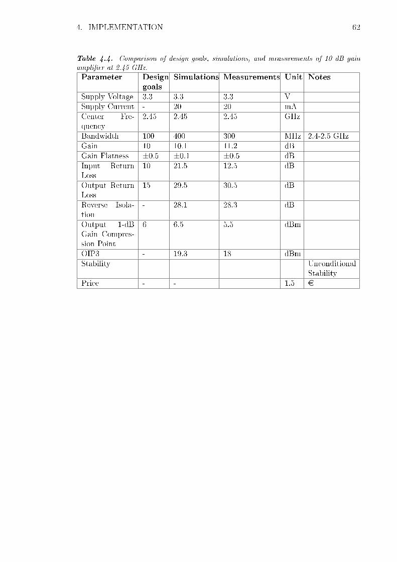
4. IMPLEMENTATION 62
Table 4.4. Comparison of design goals, simulations, and measurements of 10 dB gainamplier at 2.45 GHz.
Parameter Design
goals
Simulations Measurements Unit Notes
Supply Voltage 3.3 3.3 3.3 VSupply Current - 20 20 mACenter Fre-quency
2.45 2.45 2.45 GHz
Bandwidth 100 400 300 MHz 2.4-2.5 GHzGain 10 10.1 11.2 dBGain Flatness ±0.5 ±0.1 ±0.5 dBInput ReturnLoss
10 21.5 12.5 dB
Output ReturnLoss
15 29.5 30.5 dB
Reverse Isola-tion
- 28.1 28.3 dB
Output 1-dBGain Compres-sion Point
6 6.5 5.5 dBm
OIP3 - 19.3 18 dBmStability Unconditional
StabilityPrice - - 1.5 e

63
5. PROTOTYPING
The prototyping of the power divider is described in this chapter. This chapter
starts with the design process, which includes the connection of the 3-and 2-way
power dividers, 17 dB and 10 dB gain ampliers together. Next, the simulations
and measurements results are presented in Section 5.2 and Section 5.4 respectively.
A photograph of the prototyped power divider also presented along with the layout
generated in ADS in Section 5.3.
5.1 Design
In the previous chapter (implementation) the 3- and 2-way power dividers, 17 dB
and 10 dB gain ampliers are prototyped as a standalone devices. With this the nal
design of the power divider can be prototyped with minimum eort and also will
take less time in assembling and characterization. Moreover, the trouble shooting
becomes much easier. The block diagram showing the interconnection of the dividers
and ampliers are shown in Figure 5.1.
Signal
Generator
input
17 dB gain
amplifier
10 dB gain
amplifier
3- way Power
Divider
Auxiliary output
Auxiliary input
To Phase
shifter
input
Output for
monitoring
purpose
2- way Power Divider
Figure 5.1. Block diagram showing the interconnection of the power dividers and ampli-ers.
The topology shown in Figure 5.1 gives the exibility in conguring the SSB either
as a single channel, multi channel master or multi channel slave conguration. In the
single channel conguration (Figure 5.2), the auxiliary input and auxiliary output

5. PROTOTYPING 64
are terminated with the matched termination i.e. 50 Ω. In this conguration the
on-board signal generator (LO) provides the required RF input signal.
To Phase
shifter input
Output for
monitoring
purpose
Matched termination
Matched termination
Signal
Generator
Figure 5.2. Single channel conguration.
In multi channel master conguration, the RF input signal provided by the on-
board signal generator and is supplied to the succeeding channels. In the slave
conguration, the on-board signal generator is disabled and it gets the RF input
signal from the preceding channel. In other words, the second channel receives the
RF input signal from the rst channel, third channel from the second channel, and
so on.
A two channel conguration is shown in Figure 5.3 as an example. The channel
1 is the master which provides the RF input signal to channel 2, which is a slave
channel. The signal generator in channel 2 is disabled. The signal generator enabling
and disabling is done with the software routine. The auxiliary output of the channel
1 is connected to the auxiliary input of the channel 2. It should be mentioned that,
the disabled on-board signal generator acts as a matched termination.
To Phase
shifter input
Output for
monitoring
purpose
Matched termination
Signal
Generator
Signal
Generator
Matched termination
To Phase
shifter input
Output for
monitoring
purpose
Channel 1:
Master
Channel 2:
Slave
Auxiliary outputAuxiliary input
Figure 5.3. Two channel conguration.

5. PROTOTYPING 65
5.2 Simulation Results
The schematic that is used for simulations in ADS shown in Figure D.1 in Appendix
D. All the schematics which are used previously in developing dividers and ampliers
as standalone devices are connected together through a 50 Ω strip line. Let us label
signal generator input as LO in, auxiliary input as Aux in, to phase shifter input as
Out 1, output for monitoring purposes as Out 2, and auxiliary output as Aux out
(Figure 5.4).
LO in
17 dB gain
amplifier
10 dB gain
amplifier
3- way Power
Divider
Aux out
Aux in
Out 1
Out 2
2- way Power Divider
Figure 5.4. Block diagram showing the interconnection of the power dividers and ampli-ers and input and output ports are labeled as well.
The gain from the inputs, LO in and Aux in, to the outputs, Out 2 and Aux out,
should be 1 dB higher than to Out 1. This is desired to compensate the cable and
connector loss of approximately 1 dB (see Section 3.4). The simulated gain between
the Aux in and Out 1, Out 2, and Aux out are shown in Figure 5.5 up to 10 GHz
frequency. It is clear from the gure that the simulated gain between Aux in and
Out 1 is approximately 0 dB and between Aux in and Out 2, Aux out is around 1
dB in the operating frequency band, shown with the dark vertical lines. Similarly,
the simulated gain between the LO in and Out 1 is 0.15 dB and between LO in
and Out 2, Aux out is 0.92 dB at the center frequency of 2.45 GHz (Figure 5.6).
From these results we can conclude that the design has met all the requirements
mentioned above.

5. PROTOTYPING 66
1 1.5 2 2.5 3 3.5 4 4.5 5
x 109
−20
−15
−10
−5
0
5
Frequency [Hz]
Gai
n [d
B]
Gain vs. Frequency
Gain from Aux in to Out 1Gain from Aux in to Aux outGain from Aux in to Out 2
0.12 dB0.22 dB
1.2 dB1.1 dB
Figure 5.5. Simulated gain between the Aux in and outputs (Out 1, Out 2, and Aux out)versus frequency.
1 1.5 2 2.5 3 3.5 4 4.5 5
x 109
−25
−20
−15
−10
−5
0
5
Frequency [Hz]
Gai
n [d
B]
Gain vs. Frequency
Gain from LO in to Out 1Gain from LO in to Aux outGain from LO in to Out 2
0.2 dB
0.08 dB
0.93dB0.95 dB
Figure 5.6. Simulated gain between the LO in and outputs (Out 1, Out 2, and Aux out)versus frequency.
5.3 Layout and Fabrication
The layout was created from the schematic in ADS. The ampliers are congured in
such a way that both get the DC bias current from the single DC power supply. It
was accomplished by ipping the DC bias path of the 10 dB amplier to the other
side. The dierence can be seen in the layout shown in Figure 4.31 (a) and Figure
5.7 (a). The same substrate material that is used for ampliers was used. Similar
procedure like in ampliers was followed in milling and fabrication. The size of the
board is 39.040×34.696 mm. A photograph of the assembled power divider is shown
in Figure 5.7 (b). For debugging purposes the DC supply is given to the ampliers
through the 0 Ω resistors. These resistors are not included in the simulations.

5. PROTOTYPING 67
(a) (b)
LO in
Au
x i
n
Ou
t 1
Au
x o
ut
Out 2
VCC
Figure 5.7. Power Divider: (a) Top layer of the layout, (b) Photograph of the prototypedpower divider.
5.4 Measurement Results
The measurements are carried out with the assembled power divider as shown in
Figure 5.7 (b) in RF Laboratory. The series stability resistor Rss=14 Ω in 10 dB
gain amplier is changed to 46 Ω in order to bring down the gain to the required
value. This is the only change made to the assembled power divider. Figure 5.8
shows the measurements results of the gain from Aux in to Out 1, Out 2, and Aux
out is 0.35 dB, 1.12 dB, and 0.95 dB respectively at the center frequency of 2.45
GHz. Similarly, the measured gain from LO in to Out 1, Out 2, and Aux out
is 0.4 dB, 1.24 dB, and 1.23 dB respectively shown in Figure 5.9. The measured
and simulated reection loss at all input and output ports of the prototyped power
divider are shown in Figure 5.10 Table 5.1 shows the comparison of targeted and
measurements results at the center frequency of 2.45 GHz.
1 1.5 2 2.5 3 3.5 4 4.5 5
x 109
−20
−15
−10
−5
0
5
Frequency [Hz]
Gai
n [d
B]
Gain vs. Frequency
Measured gain Auxip to Out 1Measured gain Auxip to AuxopMeasured gain Auxip to Out 2
0.3 dB 0.4 dB
1.1 dB0.8 dB
Figure 5.8. Measured gain between the Aux in and outputs (Out 1, Out 2, and Aux out)versus frequency.

5. PROTOTYPING 68
1 1.5 2 2.5 3 3.5 4 4.5 5
x 109
−25
−20
−15
−10
−5
0
5
Frequency [Hz]
Gai
n [d
B]
Gain vs. Frequency
Measured gain from LO in to Out 1Measured gain from LO in to Aux outMeasured gain from LO in to Out 2
1.2dB1.14 dB
0.5 dB0.07 dB
Figure 5.9. Measured gain between the LO in and outputs (Out 1, Out 2, and Aux out)versus frequency.
1 1.5 2 2.5 3 3.5 4
x 109
−45
−40
−35
−30
−25
−20
−15
−10
Frequency [Hz]
Ref
lect
ion
Loss
[dB
]
Reflection Loss vs. Frequency
Measured Reflection Loss at LO in portMeasured Reflection Loss at Aux in portMeasured Reflection Loss at Out 1 portMeasured Reflection Loss at Out 2 portMeasured Reflection Loss at Aux out port
Figure 5.10. Measured and simulated reection loss of the prototyped 2.4 GHz powerdivider versus frequency.
Table 5.1. Comparison of targeted and measured gains between the input and output ports.
Targeted Simulated Measured Unit
Gain from Aux in toOut 1 0 0.25 0.35 dBOut 2 1 1.2 1.12 dBAux out 1 1.22 0.95 dB
Gain from LO in toOut 1 0 0.21 0.4 dBOut 2 1 0.96 1.24 dBAux out 1 0.96 1.23 dB

69
6. DISCUSSION
This chapter is divided into four sections. In rst section, the performance of the
prototyped 3-and 2-way resistive power dividers are discussed. The second and third
sections covers the performance of the 17 dB and 10 dB gain ampliers. Finally, in
Section 6.4 the performance of the prototyped power divider is presented.
6.1 Power Dividers
6.1.1 3-way Resistive Power Divider
The fabricated 3-way resistive power divider is using 24 Ω, ±5% tolerance, E24
series resistors instead of calculated 25 Ω resistors. The simulations are carried out
with a 24 Ω ideal resistor. The real 24 Ω resistor model from the Yageo vendor
was not available in ADS library. With the use of 24 Ω real resistor in prototyping
possibility of deviation in the resistor value is about ±1.2 Ω from the required value.
This deviation along with the substrate and practical implementation loss causes
the drift in measurement results in comparison to the simulations results. From the
Figure 4.5 it can be seen that the deviation in measurements return loss is about 2.2
dB from the simulations results at the center frequency of 2.45 GHz. This is due to
the non inclusion of real resistor in simulations and also due to dierent other factors
for example, practical implementation, component tolerances, and substrate loss..
However, the important thing to consider is whether the measured results are within
our requirement or not. Similarly, the measured insertion loss is approximately 9.88
dB, 0.38 dB higher than the calculated value of 9.5 dB at 2.45 GHz (see Figure 4.6).
The calculated value does not take into account the practical implementation loss.
It is important to note that, it is still a prototype, in the nal design the calculated
value of 25 Ω with minimum possible tolerance components should be used.
6.1.2 2-way Resistive Power Divider
The prototyped 2-way power divider is using 16 Ω resistors from the Yageo ven-
dor in the place of calculated 16.6 Ω resistors. The substrate properties, practical
implementation loss, and tolerance of the resistors results in the deviation of mea-
surements results from the simulations results can be noticed in Figure 4.11 and
Figure 4.12. The minimum measured return loss is 24 dB and maximum insertion

6. DISCUSSION 70
loss is 6.26 dB in the operating frequency band. It is important to mention that, the
actual value of 16.6 Ω with a low tolerance value should be used in the nal design.
6.2 17 dB Gain Small-Signal RF Amplier
The 17 dB gain small-signal RF amplier is prototyped using the bipolar junction
transistor BFU760F from the NXP semiconductors. The gain of 17 dB was achieved
by designing the output matching network to 17.5 dB constant gain circle plotted on
the load reection coecient plane of the Smith chart at 2.45 GHz frequency. For
compensating the non-idealities of the strip line the matching network is designed
for the constant gain circle of 17.5 dB which is 0.5 dB higher than the desired
gain. The requirement for the mass production was kept in mind while designing
the matching networks. So, the input and output matching networks are designed
only with lumped components. The fabricated amplier was optimized to meet
the required goals. The simulations, measurements return loss and gain results are
shown in Figure 4.22 and Figure 4.23 respectively. At 2.45 GHz the measured input
return loss is 12.5 dB which is 2.5 dB higher than the targeted value and output
return loss is 21.5 dB which is 6.5 dB above the desired value. The measured gain
is 17.2 dB at 2.45 GHz and is 0.2 dB above the required gain of 17 dB which is not
a signicant value. Further optimization improves the input and output return loss.
As a consequence the gain also increases which is not desired. Therefore, further
optimization was not performed. The simulations results predicted the unconditional
stability of the amplier from 0 to 10 GHz, but the measurement results (Figure 4.24)
shows potential instability at lower frequencies (less than 100 MHz). This is due to
the calibration inaccuracy of the VNA. It was veried that without the power supply
to the amplier the S11 was greater than unity. With 20 mA current consumption
the achieved output 1-dB gain compression point is 11.4 dBm at 2.45 GHz, which is,
however, 0.6 dB less than the targeted value. It is known that highly linear ampliers
normally takes high DC power. High linearity (with respect to OIP3) of 29 dBm
was achieved with 66 mW of DC power consumption. The dierence in simulations
and measurements results is due to the usage of high tolerance lumped components
in fabrication instead of tight tolerance components used in the simulations. This
is because, unavailability of the tight tolerance components in the fabrication.
Normally, the simulations results do not match with the measured results due
to practical dierences. From the tuned measurements we can see that, the dier-
ence in deviation is not a big value. Still the return loss and gain are good enough
for the application. By selecting higher operating currents the output 1-dB gain
compression point can be increased but, with the complex matching networks. Fur-
thermore, the higher currents dissipates more heat which should be avoided in our
design. By performing electromagnetic co-simulations of the strip line portion of the

6. DISCUSSION 71
circuit the measurements results can be similar to the simulated results. This way,
the time required for optimization can be minimized. But, the software which is
used for running the electromagnetic co-simulations (momentum) is expensive and
it is a time consuming process. So, instead of co-simulation procedure optimization
procedure was followed in this design. The price of all components is 1.5 euro shown
in Appendix B Table B.2. Except output 1-dB gain compression point the amplier
meets all the design requirements shown in Table 4.2.
6.3 10 dB Gain Small-Signal RF Amplier
The transistor, BFU760F, that is used for the 17 dB gain amplier was used for
this 10 dB gain amplier also. Because of the time constraint and other reasons
mentioned in Section 4.4.1. From the Figure 4.32 it can be observed that the devia-
tion in the tuned amplier measured return loss is about 10 dB from the simulated
return loss. This is due to the high sensitivity of the input return loss to the com-
ponent values. A small deviation in component values due to tolerances causes big
dierence in results. The measured gain is 1.2 dB higher than the targeted gain of
10 dB (Figure 4.33). Further optimization results in decrease of return loss. There
is a trade-o between the gain and the input return loss. However, 1.2 dB is not a
signicant value. The linearity of the amplier is 18 dBm which is lower linear than
17 dB gain amplier. Besides DC power the linearity is also function of matching
networks. The linearity is also determined with 1-dB gain compression power level.
The measured output 1-dB gain compression power level is 5.5 dBm at 2.45 GHz
which is close (0.5 dB less) to the required criteria. The bill of material of the am-
plier is 1.5 euro (see Appendix C Table C.1). All the design goals (Table 4.4) are
met excluding the output 1-dB gain compression power level.
6.4 ISM 2.4 GHz Power Divider with Highly Linear Small-
Signal RF Amplier
The gain and return loss measurements are performed on the prototyped power
divider. The deviation from the simulated gain to the measured gain between the
inputs and outputs is low. As it can be seen from the Table 5.1 a maximum of 0.28
dB deviation can be noticed between the simulated and measured results of the gain
between the LO in and outputs Out 1, Out 2, Aux out which is not a signicant
value. Similarly, 0.27 dB deviation in gain can be observed between the Aux in and
outputs Out 1, Out 2, Aux out. The measured return loss at the input and output
ports of the divider are greater than 19 dB at center frequency of 2.45 GHz (Figure
5.10). Except the change of series stability resistor Rss value of 14 Ω to 46 Ω all the
other component values are unchanged.

72
7. CONCLUSION
This thesis report presented the design of a 2.4 GHz ISM band power divider with
highly linear small-signal RF amplier. In order to realize it, 3-and 2-way power
dividers, 17 dB and 10 dB gain ampliers are prototyped as standalone devices and
integrated on a single PCB.
The 3-and 2-way resistive power dividers are constructed using resistive power di-
vider topology. The resistive topology has the advantages like, simple to implement,
broad band of operation, and compact size. Another major reason for choosing this
topology was the requirement for the mass production. It employs only lumped
components this makes it easy in mass production with less sensitivity between the
constructed dividers. The resistive power dividers are easy to reproduce and are ro-
bust. Unless otherwise specied all the presented results are measured at 2.45 GHz
in this section. It is recommend to use tight tolerance, 25 Ω and 16.6 Ω resistors
in the nal design of 3-and 2-way dividers instead of 24 Ω and 16 Ω resistors used
in prototyping. The reactive power divider topology can be evaluated as a future
work.
Important RF concepts and dierent amplier design procedures from dierent
authors are presented and are considered while prototyping the 17 dB and 10 dB
small-signal RF ampliers. The fabricated 17 dB gain amplier comprises of eleven
lumped components and one transistor. The designed and prototyped 17 dB gain
amplier has a gain of 17.2 dB, power consumption of 66 mW, and OIP3 of 29 dBm.
Furthermore, the amplier is unconditionally stable from 0 to 18 GHz. The price of
all components is 1.5 euro. The 10 dB gain amplier was designed such a way that
it is possible to re-use the layout of the 17 dB gain amplier with minor changes in
the layout. This way the total time required for designing the layout for the 10 dB
gain amplier was lowered. The only change made in the layout of the 17 dB gain
amplier was the inclusion of extra slot for the series stabilization resistor at the
collector of the transistor. The constructed 10 dB amplier has 11.2 dB gain which is
1.2 dB higher than the desired gain, power consumption of 60 mW, 5.5 dBm of output
1-dB gain compression point, and OIP3 of 18 dBm. The amplier is unconditionally
stable upto 20 GHz. Keeping in mind the requirement of reproducibility with less
sensitivity, usage of distributed components for the design of matching networks
were avoided in this design. Rogers Corporation's RO4350B LoPro, 30 mil material

7. CONCLUSION 73
used as a substrate. The simple optimization procedure was followed to meet the
design goals instead of electromagnetic co-simulations procedure.
A 2.4 GHz ISM band power divider with highly linear small-signal amplier was
realized by integrating all the power dividers and ampliers on a single substrate.
The prototyped power divider has a gain of 0.35 dB between the auxiliary input
and Out 1. And, 1.12 dB and 0.95 dB gain between the auxiliary input and Out
2, auxiliary output. Furthermore, the gain between the LO input and Out 1 is 0.4
dB. And, 1.24 dB and 1.23 dB between LO input and Out 2, auxiliary output. By
fabricating each device as a standalone device the nal prototype was built with
minimum eort and in less time. Furthermore, the cost of the power divider is
3.5 euro. The prototyped power divider is ready to be used for the needs of the
small-signal board that is used in the solid state cooking project.
It is interesting to perform electromagnetic co-simulations of the strip line portion
of the circuit as a future work. Furthermore, the 10 dB amplier can be designed
and constructed with dierent DC bias current as a further work and also with
dierent transistor. Minimum tolerance lumped components from the other vendor
can be evaluated as a further work. The Monte Carlo analysis should be performed
for the analysis of the volume manufacturability by including variability of the PCB
material and lumped components tolerances. The power divider can be evaluated
for other ISM frequency bands.
74
REFERENCES
[1] ISM Radio Bands: Will the Concept Work In the Future? [WWW]. [Ac-
cessed on: 4.7.2013]. Available: http://www.highfrequencyelectronics.com/
Archives/Dec11/1112_HFE_ism.pdf.
[2] M. Loy, R. Karingattil, and L. Williams, ISM-Band and Short Range De-
vice Regulatory Compliance Overview, Texas Instruments, Application Report,
SWRA048-May 2005.
[3] M. J. Ho, M. S. Rawles, M. Vrijkorte, and L. Fei, RF Challenges for 2.4 GHz
and 5 GHz WLAN Deployment and Design, IEEE Wireless Communications
and Networking Conference, vol. 2, pp. 783-788, Atlanta, GA, USA, March
2002.
[4] HPRF TechZone [WWW]. [Accessed on: 2.7.2013]. Available:
http://www.nxp.com/techzones/hprf-techzone/overview.html.
[5] Is Solid-State RF the Next Energy Source? [WWW]. [Accessed on: 2.7.2013].
Available: http://www.nxp.com/news/press-releases/2013/06/is-solid-state-rf-
the-next-energy-source.html.
[6] Solid State Cooking project les. Available in NXP project internal archives.
[7] Hewlett Packard, S-parameters Techniques for Faster, More Accurate Net-
work Design, Test & Measurement Application Note 95-1, Copyright Hewlett-
Packard Company, 1997.
[8] R. Ludwig and P.Bretchko, RF Circuit Design: Theory and Applications.
Prentice-Hall, Inc., 2000.
[9] P. Vizmuller, RF Design Guide: Systems, Circuits, and Equations. Artech
House, Boston, London, 1995.
[10] K. Kurokawa, Power Waves and the Scattering Matrix, IEEE Transactions
on Microwave Theory and Techniques, vol. 13, no. 2, pp. 194-202, 1965.
[11] Hewlett Packard, High-Frequency Transistor Primer: Part II, Hewlett-Packard
Co., 1993.
[12] O. P. Lunden, Active RF Circuits: Course Material, Tampere University of
Technology, 2011.
[13] C. W. Sayre, Complete Wireless Design, Second Edition. The McGraw-Hill
Companies, 2001.

REFERENCES 75
[14] W. Alan Davis and K. Agarwal, Radio Frequency Circuit Design. John Wiley
& Sons, Inc., 2001.
[15] G. Gonzalez, Microwave Transistor Ampliers: Analysis and Design, Second
Edition. Prentice-Hall, Inc., 1997.
[16] D. Woods, Reappraisal of the Unconditional Stability Criteria for Active 2-
Port Networks in Terms of S Parameters, IEEE Transactions on Circuits and
Systems, vol. 23, no. 2, pp. 73-81, February 1976.
[17] M. Lee Edwards, A New Criterion for Linear 2-Port Stability Using a Single
Geometrically Derived Parameter, IEEE Transactions on Microwave Theory
and Techniques, vol. 40, no. 12, December 1992.
[18] C. Bowick, J. Blyler, and C. Ajluni, RF Circuit Design, Second Edition. New-
ness, October 2007.
[19] G. Lombardi, Criteria for the Evaluation of Unconditional Stability of Mi-
crowave Linear Two-Ports: A Critical Review and New Proof, IEEE Transac-
tions on Microwave Theory and Technique, vol. 47, no. 6, June 1999.
[20] O. P. Lunden, Basics of RF Engineering: Course Material, Tampere University
of Technology, 2011.
[21] R. Gilmore and L. Besser, Practical RF Circuit Design for Modern Wireless
Systems: Active Circuits and Systems, Volume II, Artech House, 2003.
[22] D. K. Misra, Radio-Frequency and Microwave Communication Circuits: Anal-
ysis and Design, John Wiley & Sons, Inc., 2001.
[23] D. M. Pozar, Microwave Engineering, Fourth Edition, John Wiley & Sons, Inc.,
2011.
[24] Agilent Technologies, A Comparison of Various Bipolar Biasing Circuits, Ap-
plication Note 1293.
[25] B. Razavi, RF Microelectronics, Second Edition, Prentice Hall, 2011.
[26] P. B. Kenington, High-Linearity RF Amplier Design, Artech House, 2000.
[27] D. Cerovecki and K. Malaric, Microwave Amplier Figure of Merit Measure-
ments, Measurement Science Review, vol. 8, no. 4, 2008.
[28] R. E. Watson, Receiver Dynamic Range: Part 1, wj Tech-note, Watkins-
Johnson Company, vol. 14, no. 1, January/February 1987.

REFERENCES 76
[29] Agilent Technologies, Dierences in Application Between Power Dividers and
Power Splitters, Application Note, Agilent Technologies Inc., 2007.
[30] R. A. Johnson, Understanding Microwave Power Splitters, Microwave Jour-
nal, Santa Rosa, CA, December 1975.
[31] Wye and delta equal-split resistive splitters
[WWW]. [Accessed on: 18.3.2013]. Available:
http://www.microwaves101.com/encyclopedia/Resistive_splitters.cfm.
[32] G. D. Vendelin, A. M. Pavio, and U. L. Rohde, Microwave Circuit Design Using
Linear and Nonlinear Techniques, Second Edition, A John Wiley & Sons, Inc.,
2005.
[33] A. Grebennikov, Power Combiners, Impedance Transformers and Directional
Couplers: Part II, High Frequency Electronics, Summit Technical Media, LLC,
2008.
[34] M. Jalalifar and M. J. Uddin, Power Splitter Architectures and Applications,
Progress In Electromagnetic Research C, vol. 18, pp. 231-244, 2011.
[35] Resistive Power Dividers [WWW]. [Accessed on: 29.3.2013]. Available:
http://www.pulsarmicrowave.com/products/power_dividers/resistive.html.
[36] Power Dividers, Resistive [WWW]. [Accessed on: 5.4.2013]. Available:
http://www.aeroex.com/AMS/INMET/PDFILES/6014F.PDF.
[37] 3 way Resistive Power Divider [WWW]. [Accessed on: 10.4.2013]. Available:
http://www.jfwindustries.com/documents/50PD-292_specsheet.pdf.
[38] H. L. Krauss, C. W. Bostian, and F. H. Raab, Solid State Radio Engineering,
John Wiley & Sons, 1980.
[39] K. Chang, I. Bahl, V. Nair, S. Murarka, T. Chow, E. Allen, and R. Thallon,
RF and Microwave Circuit and Component Design for Wireless Systems, John
Wiley & Sons, Inc., December, 2011.
[40] Mouser Electronics, Electronic Components distributor [WWW]. Available:
http://www.mouser.com.
[41] Agilent Advanced Design System [WWW]. Avail-
able: http://www.home.agilent.com/products& ser-
vices/software/agilentEEsofEDAsoftware/advanceddesignsystem(ADS).

REFERENCES 77
[42] Rogers Corporation [WWW]. Available: http://www.rogerscorp.com/
acm/products/53/RO4000-LoPro-Laminates.aspx.
[43] The New LPKF ProtMat Circuit Board Plotters [WWW]. Available:
http://www.lpkf.com/_mediales/1327-next-generation-in-house-pcb-
prototyping.pdf.
[44] MWI calculator [WWW]. Available: http://www.rogerscorp.com/
acm/technology/index.aspx.
[45] N. Dye and H. Granberg, Radio Frequency Transistors: Principles and Practical
Applications, Second Edition, 2001.
[46] Advantages of modern BJTs (bipolar junction transistor) over GaAs-FETs
for low noise preamplier applications on 3.4 GHz [WWW]. [Accessed on:
8.5.2013]. Available: http://www.dl5neg.de/whitepapers/whitepapers.html.
[47] NPN wideband silicon RF transistor [WWW]. [Accessed on: 30.5.2013]. Avail-
able: http://www.nxp.com/documents/data_sheet/BFU660F.pdf.
[48] NPN wideband silicon RF transistor [WWW]. [Accessed on: 30.5.2013]. Avail-
able: http://www.nxp.com/documents/data_sheet/BFU690F.pdf.
[49] NPN wideband silicon germanium RF transis-
tor [WWW]. [Accessed on: 30.5.2013]. Available:
http://www.nxp.com/documents/data_sheet/BFU760F.pdf.
[50] A. M. Niknejad, Amplier Design Examples, University of California, Berke-
ley, 2009.
[51] Math Works [WWW]. Available: http://www.mathworks.com.
[52] Agilent Technologies, ADS 2008, Harmonic Balance Simulation, Documenta-
tion.
[53] Rogers Corporation [WWW]. Available: http://www.rogerscorp.com/ docu-
ments/726/ acm/RO4000-Laminates-Data sheet.pdf.

78
A. APPENDIX: DETAILED DATA OF
PROTOTYPED RESISTIVE POWER DIVIDERS
CPWSub MSub
S-PARAMETERS
CPW
CPW
CPW
CPW
MCROSO
Term
Term
TermTerm
S_Param
R
R
RR
MSUBCPWSUB
CPW4
CPW3
CPW2
CPW1
Cros1
Term2
Term4
Term3Term1
SP1
R2
R4
R3R1
MSub1CPWSub1
Subst="CPWSub1"W=1.5 mmG=0.8 mmL=9 mm
Subst="CPWSub1"W=1.5 mmG=0.8 mmL=9 mm
L=9 mmG=0.8 mmW=1.5 mmSubst="CPWSub1"
Subst="CPWSub1"W=1.5 mmG=0.8 mmL=9 mm
W2=1.5 mmW1=1.5 mmSubst="MSub1"
W4=1.5 mmW3=1.5 mm
Z=50 OhmNum=2
Z=50 OhmNum=4
Z=50 OhmNum=3
Z=50 OhmNum=1
Step=0.01 GHzStop=2.6 GHzStart=2.3 GHz
R=25 Ohm
R=25 Ohm
R=25 OhmR=25 Ohm
Dpeaks=Bbase=Rough=0.0006 mmTanD=0T=0.033 mmHu=1.0e+33 mmCond=5.813E+7Mur=1Er=3.66H=0.762 mm
Dpeaks=Bbase=Rough=0.0006 mmTanD=0T=0.033 mmCond=5.813E+7Mur=1Er=3.66H=0.762 mm
Figure A.1. 3-way resistive power divider simulations schematic with the ideal 24 Ωresistors at four ports along with the strip lines.
MSub
CPWSubS-PARAMETERS
S_ParamCPWSUB
MTEE_ADSCPW CPW
CPW
Term
Term
Term
R
RR
MSUB
SP2CPWSub2
Tee1CPW1 CPW2
CPW3
Term3
Term2
Term1
R3
R2R1
MSub1
Step=0.01 GHzStop=2.6 GHzStart=2.3 GHz
Dpeaks=Bbase=Rough=0.0006 mmTanD=0T=0.033 mmCond=5.813E+7Mur=1Er=3.66H=0.762 mm
W3=1.5 mmW2=1.5 mmW1=1.5 mmSubst="MSub1"
L=9 mmG=0.8 mmW=1.5 mmSubst="CPWSub1"
L=9 mmG=0.8 mmW=1.5 mmSubst="CPWSub1"
L=9 mmG=0.8 mmW=1.5 mmSubst="CPWSub1"
Z=50 OhmNum=3
Z=50 OhmNum=2
Z=50 OhmNum=1
R=16.6 Ohm
R=16.6 OhmR=16.6 Ohm
Rough=0.0006 mmBbase=Dpeaks=
Cond=5.813E+7Hu=1.0e+33 mmT=0.033 mmTanD=0
H=0.762 mmEr=3.66Mur=1
Figure A.2. 2-way resistive power divider simulations schematic with the ideal 16 Ωresistors at three ports along with the strip lines.

79
B. APPENDIX: DETAILED DATA OF
PROTOTYPED 17 DB GAIN RF AMPLIFIER
Table B.1. S-parameters of the transistor BFU760F for DC bias VCE=2.5 V and IC=20mA.
Freq-MHz
S11-mag
S11-arg
S21-mag
S21-arg
S12-mag
S12-arg
S22-mag
S22-arg
2400 0.678 179 8.02 75.07 0.05 36.27 0.273 -152.32450 0.678 178 7.86 74.47 0.05 36.43 0.272 -153.32500 0.679 177 7.7 73.86 0.051 36.54 0.271 -154.5

B. APPENDIX: Detailed Data of Prototyped 17 dB Gain RF Amplier 80
CP
WS
ubM
Sub
Sta
bFac
t
MuP
rim
eM
u
S-P
AR
AM
ET
ER
S
NE
TLI
ST
IN
CLU
DE
DC
GaC
ircl
e
GRM
15
GaC
ircle
DC
MU
RATA
Incl
ude
S_Pa
ram
Mu
MuP
rime
Stab
Fact
MSU
BCP
WSU
B
MTA
PER
MTA
PER
CPW
G
CPW
G
CPW
GCP
WG
CPW
G
CPW
G
MCU
RVE
MCU
RVE
MTE
E_A
DS
MTE
E_A
DS
MTE
E_A
DS
MLI
N
MLI
N
MLI
N
MLI
N
MLI
N
MLI
N
MLI
N
LLQ
P15
LQW
15
V_D
C
Term
Term
R
R
R
GRM
15G
RM15
GRM
15
GRM
15
GRM
15
rfss
_v2_
2_lib
_bfu
760f
_spi
ce_s
chem
atic
Cout
GaC
ircle
1
DC1
muR
ata
SP1
Mu1
MuP
rime1
Stab
Fact
1
MSu
b1CP
WSu
b1
Tape
r2
Tape
r1
CPW
6
CPW
5
CPW
3CP
W2
CPW
1
CPW
4
Curv
e2Cu
rve1
Tee3
Tee2
Tee1
TL1
TL4
TL3
TL5
TL2
TL7
TL6
LeLi
nm
Lout
m
Vcc
Term
2
Term
1Rp
s
Rb
Rc
Cinm
Cin
Cout
m
Cdcs
2
Cdcs
1
BJT
PartN
umbe
r=G
RM15
55C1
H10
0JZ0
1
GaC
ircle
1=ga
_circ
le(S
,2,5
1)
Step
=0.0
1 G
Hz
Stop
=10.
0 G
Hz
Star
t=10
.0 M
Hz
Mu1
=mu(
S)M
uPrim
e1=m
u_pr
ime(
S)
Stab
Fact
1=sta
b_fa
ct(S
)
Dpe
aks=
Bbas
e=Ro
ugh=
0.00
06 m
mTa
nD=0
T=0.
033
mm
Hu=
1.0e
+33
mm
Cond
=5.8
13E+
7M
ur=1
Er=3
.55
H=0
.779
mm
Dpe
aks=
Bbas
e=Ro
ugh=
0.00
06 m
mTa
nD=0
T=0.
033
mm
Cond
=5.8
13E+
7M
ur=1
Er=3
.55
H=0
.779
mm
L=1.
5 m
mW
2=0.
6 m
mW
1=1.
705
mm
Subs
t="M
Sub1
"
L=1.
5 m
mW
2=0.
6 m
mW
1=1.
705
mm
Subs
t="M
Sub1
"L=
5 m
mG
=1.2
mm
W=1
.705
mm
Subs
t="C
PWSu
b1"
L=0.
9 m
mG
=1.2
mm
W=1
.705
mm
Subs
t="C
PWSu
b1"
L=0.
9 m
mG
=1.2
mm
W=1
.705
mm
Subs
t="C
PWSu
b1"
L=1.
8 m
mG
=1.2
mm
W=1
.705
mm
Subs
t="C
PWSu
b1"
L=5
mm
G=1
.2 m
mW
=1.7
05 m
mSu
bst=
"CPW
Sub1
"
L=1.
8 m
mG
=1.2
mm
W=1
.705
mm
Subs
t="C
PWSu
b1"
Radi
us=1
.0 m
mA
ngle
=90
W=0
.808
1 m
mSu
bst=
"MSu
b1"
Radi
us=1
.0 m
mA
ngle
=90
W=0
.808
1 m
mSu
bst=
"MSu
b1"
W3=
0.80
81 m
mW
2=1.
705
mm
W1=
1.70
5 m
mSu
bst=
"MSu
b1"
W3=
0.80
81 m
mW
2=0.
8081
mm
W1=
0.80
81 m
mSu
bst=
"MSu
b1"
W3=
0.80
81 m
mW
2=1.
705
mm
W1=
1.70
5 m
mSu
bst=
"MSu
b1"
L=1.
0 m
mW
=1.7
05 m
mSu
bst=
"MSu
b1"
L=4
mm
W=0
.808
1 m
mSu
bst=
"MSu
b1"
L=1.
0000
000
mm
W=0
.808
1 m
mSu
bst=
"MSu
b1"
L=1.
0000
000
mm
W=0
.808
1 m
mSu
bst=
"MSu
b1"
L=3.
45 m
mW
=0.8
081
mm
Subs
t="M
Sub1
"
L=1
mm
W=1
.705
mm
Subs
t="M
Sub1
"
L=1.
4 m
mW
=0.8
081
mm
Subs
t="M
Sub1
"
L=0.
2 nH
PartN
umbe
r=LQ
P15M
N2N
8W02
PartN
umbe
r=LQ
W15
AN
4N7C
00
Vdc
=3.3
V
Z=50
Ohm
Num
=2
Z=50
Ohm
Num
=1R=
390
Ohm
R=40
kO
hm
R=40
Ohm
PartN
umbe
r=G
RM15
55C1
H3R
0WA
01Pa
rtNum
ber=
GRM
1555
C1H
100J
Z01
PartN
umbe
r=G
RM15
55C1
H11
0JA
01
PartN
umbe
r=G
RM15
5C71
H10
4KE1
9
PartN
umbe
r=G
RM15
55C1
H18
1GA
01
Figure B.1. Complete ADS schematic of the 17 dB gain RF Amplier used for simulationspresented in Section 4.3.4.

B. APPENDIX: Detailed Data of Prototyped 17 dB Gain RF Amplier 81
Please note that the prices of the components are in the order of minimum number
of fty components. The prices are from Mouser electronics [38] on the date 7 July,
2013.
Table B.2. Bill of Material of 17 dB gain RF amplier.
Component Package Price in eBJT SOT343F 0.273Rc 0402 0.0001Rb 0402 0.0001Rps 0402 0.0001Linm 0402 0.1Loutm 0402 0.218Cin 0402 0.018Cinm 0402 0.018Cout 0402 0.018Coutm 0402 0.018Cdcs1 0402 0.018Cdcs2 0402 0.018PCB - 0.5

82
C. APPENDIX: DETAILED DATA OF
PROTOTYPED 10 DB GAIN RF AMPLIFIER
DC
MuP
rim
eM
u
S-P
AR
AM
ET
ER
S
NE
TLI
ST
IN
CLU
DE
CP
WS
ubM
Sub
Sta
bFac
t
Stab
Fact
MSU
BCP
WSU
B
GRM
15G
RM15
GRM
15
GRM
15
MU
RATA
Incl
ude
S_Pa
ram
Mu
MuP
rime
LQP1
5
MLI
N
MLI
N
MLI
N
R
V_D
C
MLI
N
MLI
NM
TEE_
AD
S
MLI
N
MTE
E_A
DS
R
GRM
15
GRM
15
CPW
GCP
WG
CPW
G
CPW
G
CPW
GCP
WG
DC
LQW
15
MLI
N
rfss
_v2_
2_lib
_bfu
760f
_spi
ce_s
chem
atic
Term
Term
MLI
N
RR
MTA
PER
MTA
PER
L
MCU
RVE
MCU
RVE
MTE
E_A
DS
Sim
ulat
ed
MSu
b1CP
WSu
b1
C1C2
C5
C6
muR
ata
SP1
Mu1
MuP
rime1
L1
TL3
TL6
TL7
R1
SRC1
TL1
TL8
Tee1
3
C3TL
5
Tee1
R2
C4
CPW
4CP
W5
CPW
2
CPW
6
CPW
1CP
W3
DC1
L2
TL2
BJT
Term
1
Term
2
TL4
R4R3
Tape
r2
Tape
r1
Le
Curv
e2Cu
rve1
Tee2
Sim
ulat
ed=s
tab_
fact
(S)
Dpe
aks=
Bbas
e=Ro
ugh=
0.00
06 m
mTa
nD=0
T=0.
033
mm
Hu=
1.0e
+33
mm
Cond
=5.8
13E+
7M
ur=1
Er=3
.55
H=0
.779
mm
Dpe
aks=
Bbas
e=Ro
ugh=
0.00
06 m
mTa
nD=0
T=0.
033
mm
Cond
=5.8
13E+
7M
ur=1
Er=3
.55
H=0
.779
mm
PartN
umbe
r=G
RM15
55C1
H10
1GA
01Pa
rtNum
ber=
GRM
1555
C1H
1R3W
A01
PartN
umbe
r=G
RM15
55C1
H10
0GA
01
PartN
umbe
r=G
RM15
55C1
H10
1GA
01
Step
=0.0
1 G
Hz
Stop
=10.
0 G
Hz
Star
t=10
.0 M
Hz
Mu1
=mu(
S)M
uPrim
e1=m
u_pr
ime(
S)
PartN
umbe
r=LQ
P15M
N2N
0W02
L=1.
0 m
mW
=0.8
081
mm
Subs
t="M
Sub1
"
L=0.
3000
000
mm
W=0
.808
1 m
mSu
bst=
"MSu
b1"
L=1
mm
W=1
.705
mm
Subs
t="M
Sub1
"
R=36
kO
hm
L=1.
0 m
mW
=1.7
05 m
mSu
bst=
"MSu
b1"
L=1
mm
W=1
.705
mm
Subs
t="M
Sub1
"Su
bst=
"MSu
b1"
W1=
1.70
5 m
mW
2=1.
705
mm
W3=
0.80
81 m
m
PartN
umbe
r=G
RM15
5C81
E104
KA
12Su
bst=
"MSu
b1"
Subs
t="M
Sub1
"W
1=1.
705
mm
W2=
1.70
5 m
mW
3=0.
8081
mm
R=24
Ohm
PartN
umbe
r=G
RM15
55C1
H18
1GA
01
Vdc
=3.3
V
L=1.
8 m
mG
=1.2
mm
W=1
.705
mm
Subs
t="C
PWSu
b1"
L=0.
9 m
mG
=1.2
mm
W=1
.705
mm
Subs
t="C
PWSu
b1"
L=1.
8 m
mG
=1.2
mm
W=1
.705
mm
Subs
t="C
PWSu
b1"
L=5
mm
G=1
.2 m
mW
=1.7
05 m
mSu
bst=
"CPW
Sub1
"
L=5
mm
G=1
.2 m
mW
=1.7
05 m
mSu
bst=
"CPW
Sub1
"
L=0.
9 m
mG
=1.2
mm
W=1
.705
mm
Subs
t="C
PWSu
b1"
PartN
umbe
r=LQ
W15
AN
4N7C
00
W=0
.808
1 m
mSu
bst=
"MSu
b1"
W=0
.808
1 m
mL=
0.30
0000
0 m
m
Z=50
Ohm
Num
=1
Z=50
Ohm
Num
=2
Subs
t="M
Sub1
"
L=4
mm
W=0
.808
1 m
m
L=1.
6 m
m
R=75
Ohm
R=14
Ohm
L=1.
5 m
mW
2=0.
6 m
mW
1=1.
705
mm
Subs
t="M
Sub1
"
L=1.
5 m
mW
2=0.
6 m
mW
1=1.
705
mm
Subs
t="M
Sub1
"
L=0.
2 nH
Subs
t="M
Sub1
"
W3=
0.80
81 m
mW
2=0.
8081
mm
Subs
t="M
Sub1
"
W=0
.808
1 m
mSu
bst=
"MSu
b1"
Ang
le=9
0Ra
dius
=1.5
mm
W1=
0.80
81 m
m
Radi
us=1
.5 m
mA
ngle
=90
W=0
.808
1 m
m
Figure C.1. Complete ADS schematic of the 10 dB gain RF Amplier used for simulationspresented in Section 4.4.3.

C. APPENDIX: Detailed Data of Prototyped 10 dB Gain RF Amplier 83
Please note that the prices of the components are in the order of minimum number
of fty components. The prices are from Mouser electronics [38] on the date 7 July,
2013.
Table C.1. Bill of Material of 10 dB gain RF amplier.
Component Package Price in eBJT SOT343F 0.273Rc 0402 0.0001Rb 0402 0.0001Rps 0402 0.0001Rss 0402 0.0001Linm 0402 0.1Loutm 0402 0.218Cin 0402 0.018Cinm 0402 0.018Cout 0402 0.018Coutm 0402 0.018Cdcs1 0402 0.018Cdcs2 0402 0.018PCB - 0.5

84
D. APPENDIX: DETAILED DATA OF 2.4 GHZ
POWER DIVIDER WITH HIGHLY LINEAR
SMALL-SIGNAL RF AMPLIFIER
DC
MuP
rim
eM
u
S-P
AR
AM
ET
ER
S
NE
TLI
ST
IN
CLU
DE
CP
WS
ubM
Sub
Sta
bFac
t
Sta
bFac
t
MS
UB
CP
WS
UB
MU
RAT
AIn
clud
e
S_P
aram
Mu
MuP
rim
e
LQP
15
V_D
C
MT
EE
_AD
S
MT
EE
_AD
S
MT
EE
_AD
S
LQW
15
MLI
N
MLI
N
MLI
N
MLI
N
MLI
N
MLI
N
MLI
N
MLI
N
CP
WG
CP
WG
CP
WG
CP
WG
CP
WG
CP
WG
DC
GR
M15
GR
M15
GR
M15
GR
M15
GR
M15
GR
M15
rfss
_v2_
2_lib
_bfu
760f
_spi
ce_s
chem
atic
Term
MC
UR
VE
MC
UR
VE
R
R
R
MT
EE
_AD
S
CP
W
CP
W
L
MTA
PE
R
Term
Term
MTA
PE
R
R
RR
MTA
PE
R
MTA
PE
RC
PW
G
CP
WG
CP
WG
CP
WG
CP
WG
CP
WG
MC
UR
VE
MC
UR
VE
MT
EE
_AD
S
MT
EE
_AD
S
MT
EE
_AD
S
MLI
N
MLI
N
MLI
N
MLI
N
MLI
N
MLI
N
MLI
N
LLQ
P15
LQW
15
V_D
C
R
R
R
R
GR
M15
GR
M15
GR
M15
GR
M15
GR
M15
GR
M15
rfss
_v2_
2_lib
_bfu
760f
_spi
ce_s
chem
atic
CP
W
CP
W
MC
RO
SO
Term
Term
RR
RR
Sim
ulat
ed
MS
ub1
CP
WS
ub1
muR
ata1
SP
1
Mu2
MuP
rim
e2
L4
SR
C1
Tee1
4
Tee1
3
Tee5
L3
TL1
5
TL1
4
TL1
3
TL1
2
TL1
1
TL1
0
TL9
TL8
CP
W19
CP
W18
CP
W17
CP
W16
CP
W15
CP
W14
DC
2
C12
C11
C10
C9
C8
C7
BJT
1
Term
2
Cur
ve4
Cur
ve3
R14
R13
R12
R11
Tee4
CP
W12
CP
W11
Le1
Tape
r3
Term
3
Term
4
R10
R9
R8
Tape
r1
Tape
r2C
PW
10
CP
W9
CP
W8
CP
W7
CP
W5
CP
W6
Cur
ve1
Cur
ve2
Tee1
Tee2
Tee3
TL6
TL7
TL2
TL5
TL3
TL4
TL1
LeL1
L2
Vcc
R7
R6
R5
C4
C3
C6
C5
C1
C2
BJT
CP
W4
CP
W2
Cro
s1
Term
1
Term
5
R1
R3
R4
R2
Tape
r4
Sim
ulat
ed=s
tab_
fact
(S)
Dpe
aks=
Bba
se=
Rou
gh=0
.000
6 m
mTa
nD=0
T=0
.033
mm
Hu=
1.0e
+33
mm
Con
d=5.
813E
+7M
ur=1
Er=
3.55
H=0
.779
mm
Dpe
aks=
Bba
se=
Rou
gh=0
.000
6 m
mTa
nD=0
T=0
.033
mm
Con
d=5.
813E
+7M
ur=1
Er=
3.55
H=0
.779
mm
Ste
p=0.
01 G
Hz
Sto
p=10
.0 G
Hz
Sta
rt=1
0.0
MH
z
Mu1
=mu(
S)
MuP
rim
e1=m
u_pr
ime(
S)
Par
tNum
ber=
LQP
15M
N2N
0W02
Vdc
=3.3
V W3=
0.80
81 m
mW
2=0.
8081
mm
W1=
0.80
81 m
mS
ubst
="M
Sub
1"
W3=
0.80
81 m
mW
2=1.
705
mm
W1=
1.70
5 m
mS
ubst
="M
Sub
1"
W3=
0.80
81 m
mW
2=1.
705
mm
W1=
1.70
5 m
mS
ubst
="M
Sub
1"
Par
tNum
ber=
LQW
15A
N4N
7C00
L=0.
3000
000
mm
W=0
.808
1 m
mS
ubst
="M
Sub
1"
L=1
mm
W=1
.705
mm
Sub
st="
MS
ub1"
L=1.
0 m
mW
=1.7
05 m
mS
ubst
="M
Sub
1"
L=1
mm
W=1
.705
mm
Sub
st="
MS
ub1"
L=0.
3000
000
mm
W=0
.808
1 m
mS
ubst
="M
Sub
1"
L=1.
0 m
mW
=0.8
081
mm
Sub
st="
MS
ub1"
L=1.
6 m
mW
=0.8
081
mm
Sub
st="
MS
ub1"
L=4
mm
W=0
.808
1 m
mS
ubst
="M
Sub
1"
L=1.
8 m
mG
=1.2
mm
W=1
.705
mm
Sub
st="
CP
WS
ub1"
L=0.
9 m
mG
=1.2
mm
W=1
.705
mm
Sub
st="
CP
WS
ub1"
L=1.
8 m
mG
=1.2
mm
W=1
.705
mm
Sub
st="
CP
WS
ub1"
L=5
mm
G=1
.2 m
mW
=1.7
05 m
mS
ubst
="C
PW
Sub
1"
L=2
mm
G=1
.2 m
mW
=1.7
05 m
mS
ubst
="C
PW
Sub
1"
L=0.
9 m
mG
=1.2
mm
W=1
.705
mm
Sub
st="
CP
WS
ub1"
Par
tNum
ber=
GR
M15
55C
1H10
1GA
01
Par
tNum
ber=
GR
M15
55C
1H1R
3WA
01
Par
tNum
ber=
GR
M15
55C
1H10
1GA
01
Par
tNum
ber=
GR
M15
55C
1H10
1GA
01
Par
tNum
ber=
GR
M15
5C81
E10
4KA
12
Par
tNum
ber=
GR
M15
55C
1H18
1GA
01
Z=5
0 O
hmN
um=2
Rad
ius=
1.5
mm
Ang
le=9
0W
=0.8
081
mm
Sub
st="
MS
ub1"
Rad
ius=
1.5
mm
Ang
le=9
0W
=0.8
081
mm
Sub
st="
MS
ub1"
R=3
6 kO
hm
R=2
4 O
hm
R=7
5 O
hmR
=46
Ohm
W3=
1.70
5 m
mW
2=1.
705
mm
W1=
1.70
5 m
mS
ubst
="M
Sub
1"L=
6 m
mG
=1.2
mm
W=1
.705
mm
Sub
st="
CP
WS
ub1"
L=7.
5 m
mG
=1.2
mm
W=1
.705
mm
Sub
st="
CP
WS
ub1"
L=0.
2 nH
Num
=3Z
=50
Ohm
Num
=4Z
=50
Ohm
W1=
1.70
5 m
mW
2=0.
6 m
mL=
1.5
mm
R=1
6.6
Ohm
R=1
6.6
Ohm
R=1
6.6
Ohm
L=1.
5 m
mW
2=0.
6 m
mW
1=1.
705
mm
Sub
st="
MS
ub1"
L=1.
5 m
mW
2=0.
6 m
mW
1=1.
705
mm
Sub
st="
MS
ub1"
L=1.
8 m
mG
=1.2
mm
W=1
.705
mm
Sub
st="
CP
WS
ub1"
L=2
mm
G=1
.2 m
mW
=1.7
05 m
mS
ubst
="C
PW
Sub
1"
L=1.
8 m
mG
=1.2
mm
W=1
.705
mm
Sub
st="
CP
WS
ub1"
L=0.
9 m
mG
=1.2
mm
W=1
.705
mm
Sub
st="
CP
WS
ub1"
L=0.
9 m
mG
=1.2
mm
W=1
.705
mm
Sub
st="
CP
WS
ub1"
L=5
mm
G=1
.2 m
mW
=1.7
05 m
mS
ubst
="C
PW
Sub
1"
Rad
ius=
1.0
mm
Ang
le=9
0W
=0.8
081
mm
Sub
st="
MS
ub1"
Rad
ius=
1.0
mm
Ang
le=9
0W
=0.8
081
mm
Sub
st="
MS
ub1"
W3=
0.80
81 m
mW
2=1.
705
mm
W1=
1.70
5 m
mS
ubst
="M
Sub
1"
W3=
0.80
81 m
mW
2=0.
8081
mm
W1=
0.80
81 m
mS
ubst
="M
Sub
1"
W3=
0.80
81 m
mW
2=1.
705
mm
W1=
1.70
5 m
mS
ubst
="M
Sub
1"
L=1.
4 m
mW
=0.8
081
mm
Sub
st="
MS
ub1"
L=1
mm
W=1
.705
mm
Sub
st="
MS
ub1"
L=3.
45 m
mW
=0.8
081
mm
Sub
st="
MS
ub1"
L=1.
0000
000
mm
W=0
.808
1 m
mS
ubst
="M
Sub
1"
L=1.
0000
000
mm
W=0
.808
1 m
mS
ubst
="M
Sub
1"
L=4
mm
W=0
.808
1 m
mS
ubst
="M
Sub
1"
L=1.
0 m
mW
=1.7
05 m
mS
ubst
="M
Sub
1"
L=0.
2 nH
Par
tNum
ber=
LQP
15M
N2N
4W02
Par
tNum
ber=
LQW
15A
N4N
7C00
Vdc
=3.3
V
W1=
1.70
5 m
mW
2=0.
6 m
mL=
1.5
mm
R=2
4 O
hm
R=3
6 kO
hm
R=3
90 O
hm
Par
tNum
ber=
GR
M15
55C
1H18
1GA
01
Par
tNum
ber=
GR
M15
5C71
H10
4KE
19
Par
tNum
ber=
GR
M15
55C
1H12
0GA
01
Par
tNum
ber=
GR
M15
55C
1H10
0JZ
01
Par
tNum
ber=
GR
M15
55C
1H10
0JZ
01P
artN
umbe
r=G
RM
1555
C1H
1R5B
A01
Sub
st="
MS
ub1"
Sub
st="
MS
ub1"
L=8
mm
G=1
.2 m
mW
=1.7
05 m
mS
ubst
="C
PW
Sub
1"
L=6
mm
G=1
.2 m
mW
=1.7
05 m
mS
ubst
="C
PW
Sub
1"
W4=
1.70
5 m
mW
3=1.
705
mm
W2=
1.70
5 m
mW
1=1.
705
mm
Sub
st="
MS
ub1"
Z=5
0 O
hmN
um=1
Z=5
0 O
hmN
um=5
R=2
5 O
hmR
=25
Ohm
R=2
5 O
hm
R=2
5 O
hm
Figure D.1. ADS schematic of the complete integration of the power dividers and ampli-ers used for simulations presented in Section 5.2.