BD Cytometric Bead Array: Multiplexed Bead-Based Immunoassays
Agilent Medalist Bead Probe TechnologyCustomer Viewable
May 2007Page 1
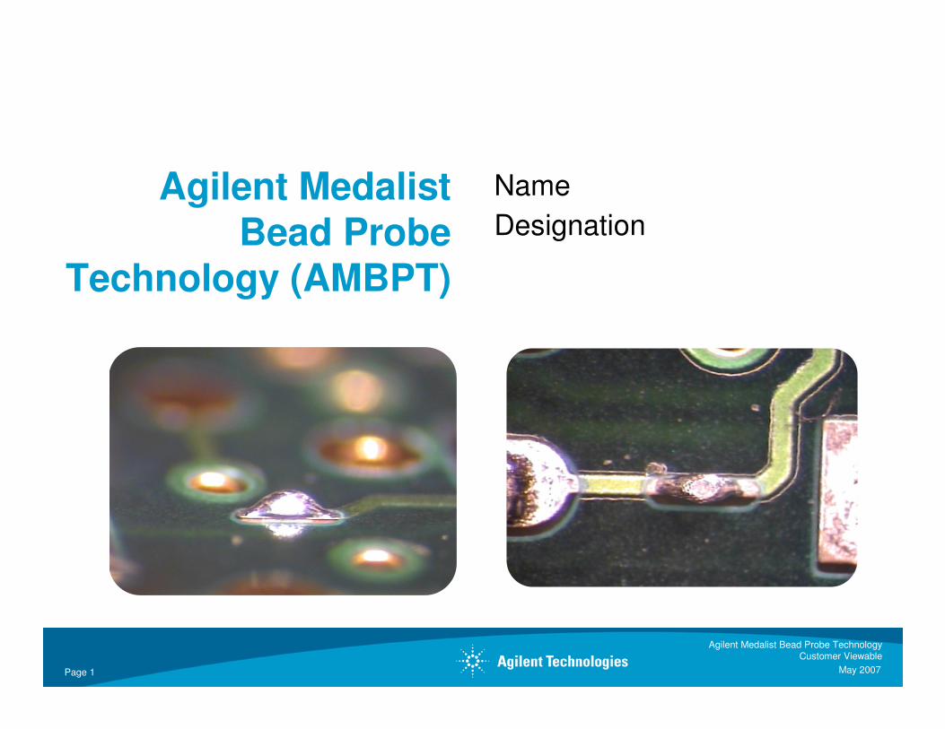
Agilent Medalist Bead Probe
Technology (AMBPT)
Name
Designation
Agilent Medalist Bead Probe TechnologyCustomer Viewable
May 2007Page 2
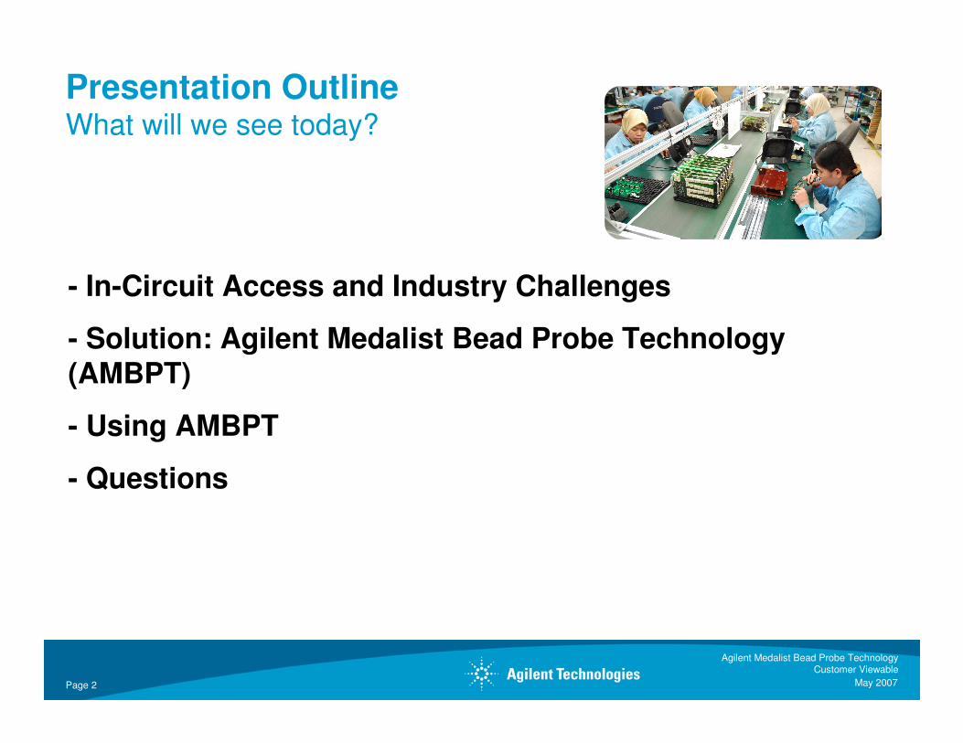
Presentation OutlineWhat will we see today?
- In-Circuit Access and Industry Challenges
- Solution: Agilent Medalist Bead Probe Technology (AMBPT)
- Using AMBPT
- Questions

Agilent Medalist Bead Probe TechnologyCustomer Viewable
May 2007Page 3
In-Circuit AccessWhat’s the Problem ?
No layout space for targets
– Board density increasing rapidly
• More devices, smaller devices, with more device pins – more densely packed
• Finer trace-space routing – tighter routing restrictions
Targets affect board performance at higher frequencies
– Targets are 3 to 6 times wider than traces (e.g., 30 mil target on 5 mil
trace)
• Big targets present a lumped capacitance to ground somewhere mid-trace
• Lumped capacitance creates an impedance mismatch – causes reflections

Agilent Medalist Bead Probe TechnologyCustomer Viewable
May 2007Page 4
In-Circuit AccessWhat’s the Problem ?
Board designer perceives unacceptable schedule and performance risks due to “non-value-added” test requirements
– Adding test points disturbs the “best” layout, may hurt performance
– Takes time and skill to do, yet can’t do all that are requested
– Causes friction between Design and Test Departments
No test points, ideal layout
IC 1 IC 2
Two added test points
IC 1 IC 2

Agilent Medalist Bead Probe TechnologyCustomer Viewable
May 2007Page 5
Solution: Agilent Medalist Bead Probe TechnologyA New Way of Looking at Access
New Way (Close Up):
• Place target in the Fixture
• Hit it with a pointed probe
on the Board
Old Way (Close Up):
• Place target on the Board
• Hit it with a pointed probe
in the Fixture
Fixture
TargetProbe
Board
Fixture
Target Probe
Board

Agilent Medalist Bead Probe TechnologyCustomer Viewable
May 2007Page 6
Solution: Agilent Medalist Bead Probe Technology

Agilent Medalist Bead Probe TechnologyCustomer Viewable
May 2007Page 7
Solution: Agilent Medalist Bead Probe TechnologySectional views
Bead
FR4
Trace MaskSolder
EndSection
Bead
FR4
SideSection
Trace
Agilent Medalist Bead Probe TechnologyCustomer Viewable
May 2007Page 8
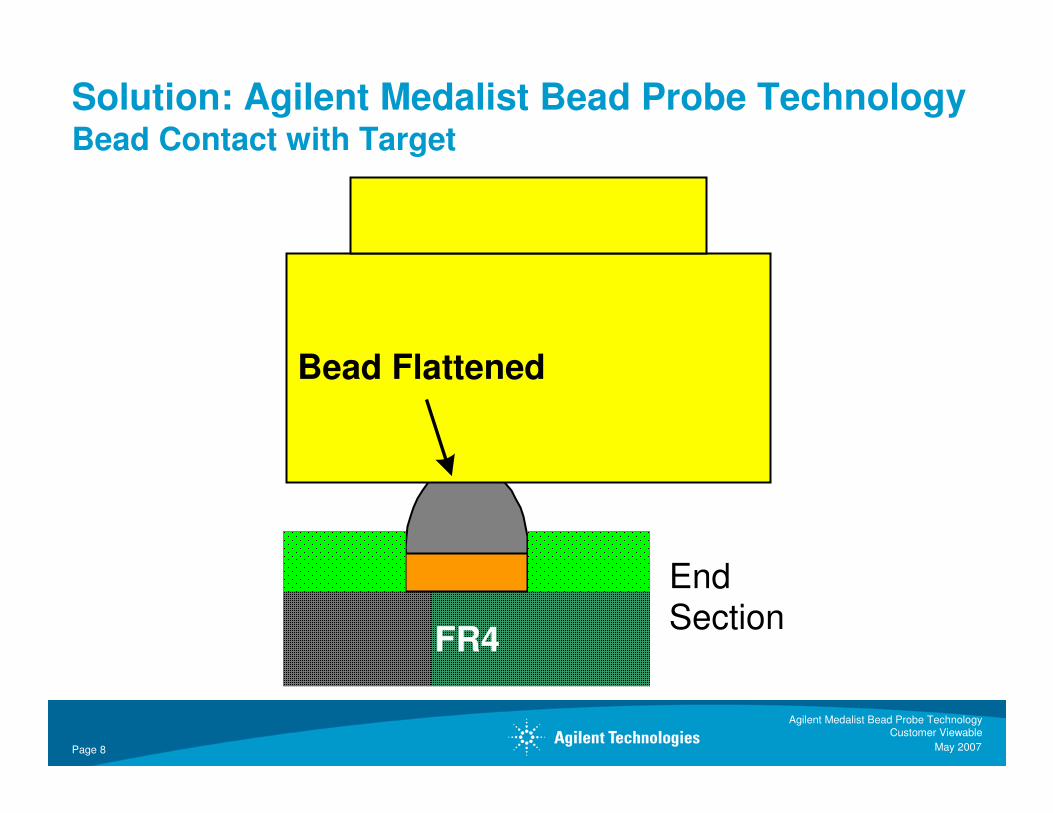
Solution: Agilent Medalist Bead Probe TechnologyBead Contact with Target
FR4
EndSection
Bead Flattened

Agilent Medalist Bead Probe TechnologyCustomer Viewable
May 2007Page 9
Wiping Action of Test Probes
- Pointing error inherent to test probes
- As the plunger draws back to the barrel, the tip of probe swings back and forth a few times.
- This creates “wiping action”
- Provide good contact after initial deformation

Agilent Medalist Bead Probe TechnologyCustomer Viewable
May 2007Page 10
Solution: Agilent Medalist Bead Probe TechnologyBead probes take on the width of the underlying trace and therefore provide “Layout Independent Test Points”.We don’t have to change the layout to get test access !

Agilent Medalist Bead Probe TechnologyCustomer Viewable
May 2007Page 11
Solution: Agilent Medalist Bead Probe TechnologyBead probes, compared to standard test pads have virtually no performance impact.
Source: “A New Probing Technique for High-Speed/High-Density Printed Circuit Boards”, K. P. Parker, International Test Conference, paper 13.1, Oct 2004, Charlotte NC, reprinted with permission.
30 80 130 180 230 280 330 380-20 420
0.0
0.4
0.8
1.2
1.6
2.0
2.4
-0.4
2.8
time, psec
p_
idea
l_5_
3_0
Voltag
e
30 80 130 180 230 280 330 380-20 420
0.0
0.4
0.8
1.2
1.6
2.0
2.4
-0.4
2.8
time, psecp_
ST
D_5_3_
0V
oltag
e
Ideal Trace Trace with 35 mil test target

Agilent Medalist Bead Probe TechnologyCustomer Viewable
May 2007Page 12
Solution: Agilent Medalist Bead Probe TechnologyBead probes, compared to standard test pads have virtually no performance impact.
Source: “A New Probing Technique for High-Speed/High-Density Printed Circuit Boards”, K. P. Parker, International Test Conference, paper 13.1, Oct 2004, Charlotte NC, reprinted with permission.
30 80 130 180 230 280 330 380-20 420
0.0
0.4
0.8
1.2
1.6
2.0
2.4
-0.4
2.8
time, psec
p_
idea
l_5_
3_0
Voltag
e
Ideal Trace Trace with 9 bead probes
30 80 130 180 230 280 330 380-20 420
0.0
0.4
0.8
1.2
1.6
2.0
2.4
-0.4
2.8
time, psecP
_B
EA
D_5_
3_9
Voltag
e
Agilent Medalist Bead Probe TechnologyCustomer Viewable
May 2007Page 13
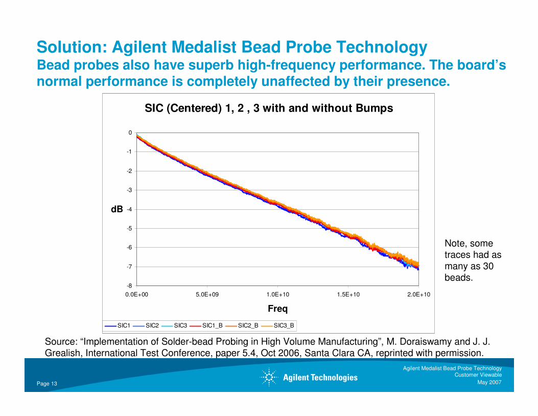
Solution: Agilent Medalist Bead Probe TechnologyBead probes also have superb high-frequency performance. The board’s normal performance is completely unaffected by their presence.
SIC (Centered) 1, 2 , 3 with and without Bumps
-8
-7
-6
-5
-4
-3
-2
-1
0
0.0E+00 5.0E+09 1.0E+10 1.5E+10 2.0E+10
Freq
dB
SIC1 SIC2 SIC3 SIC1_B SIC2_B SIC3_B
Source: “Implementation of Solder-bead Probing in High Volume Manufacturing”, M. Doraiswamy and J. J. Grealish, International Test Conference, paper 5.4, Oct 2006, Santa Clara CA, reprinted with permission.
Note, some traces had as many as 30 beads.

Agilent Medalist Bead Probe TechnologyCustomer Viewable
May 2007Page 14
Solution: Agilent Medalist Bead Probe TechnologyHow are bead probes made? (The short story)
Bead Probes are created using standard solder paste/reflow technology
– No new processing steps are required
– No unusual masking, stenciling or soldering parameters are required
There are two, similar types of Bead Probes
– Soldermask-defined Beads (on planar copper)
– Metal-defined Beads (on signal traces)
Manufactured the same way
– Open a hole in the soldermask over desired Bead location
– Apply paste with a stencil aperture (same step as all other paste applied)
– Reflow (same process as all other paste is reflowed)

Agilent Medalist Bead Probe TechnologyCustomer Viewable
May 2007Page 15
Solution: Agilent Medalist Bead Probe TechnologyHow are Bead Probes made? (The short story)
Cu Trace
Cu Trace
Stackup
Solder Mask Opening Solder Stencil Opening
Stackup
W
L
D

Agilent Medalist Bead Probe TechnologyCustomer Viewable
May 2007Page 16
Solution: Agilent Medalist Bead Probe TechnologyHow are bead probes made? (The short story)After stenciling, a paste brick remains that flows into a bead upon heating.

Agilent Medalist Bead Probe TechnologyCustomer Viewable
May 2007Page 17
Video Animation of Bead Probe Fabrication
Run video to show Bead Probe Fabrication

Agilent Medalist Bead Probe TechnologyCustomer Viewable
May 2007Page 18
THE
IMPLICATIONS
ItItItIt’’’’s proven. s proven. s proven. s proven. ItItItIt’’’’s been done ...s been done ...s been done ...s been done ...Just got to do it the right way.Just got to do it the right way.Just got to do it the right way.Just got to do it the right way.

Agilent Medalist Bead Probe TechnologyCustomer Viewable
May 2007Page 19
Fixture vendors
Headless probes
Spring force as per recommendation

Agilent Medalist Bead Probe TechnologyCustomer Viewable
May 2007Page 20
Contract Manufacturers
Solder paste mix
Stencil aperture sizing
Reflow
Rework steps

Agilent Medalist Bead Probe TechnologyCustomer Viewable
May 2007Page 21
Probe Makers
Flat-face headless probes

Agilent Medalist Bead Probe TechnologyCustomer Viewable
May 2007Page 22
CAD Engineers
Solder mask opening
Test attributes

Agilent Medalist Bead Probe TechnologyCustomer Viewable
May 2007Page 23
Expanding coverage opens doors
VTEP
iVTEP
NPM

Agilent Medalist Bead Probe TechnologyCustomer Viewable
May 2007Page 24
Agilent Intellectual Property
- 16 patents and patents-pending
- Filed in the USA and other countries

Agilent Medalist Bead Probe TechnologyCustomer Viewable
May 2007Page 25
Licensing
Types of licenses :
• Customer license
• Equipment license
(for test equipment vendors)

Agilent Medalist Bead Probe TechnologyCustomer Viewable
May 2007Page 26
Process for obtaining a Customer License
• Go to www.agilent.com/see/beadprobe
• Complete the licensing web-form
• A copy of the license agreement will be made
available to you
• You will be contacted by Agilent
• Return the signed agreement to Agilent
• Agilent counter-signs and returns the agreement
plus the Bead Probe Handbook

Agilent Medalist Bead Probe TechnologyCustomer Viewable
May 2007Page 27
AMBPT wins prestigious EDN Innovation Award of the Year (2007) EM Asia Innovation Award 2007
- Based on product released in 2006. (AMBPT was launched Nov 2006)
- Results and ceremony on 3rd April 07.
- Agilent Medalist Bead Probe announced as Innovation of the Year
- Dr Ken Parker named as one of the finalist for Innovator of the Year
- http://www.edn.com/index.asp?layout=InnovationAwardComp&year=2006&order=55

Agilent Medalist Bead Probe TechnologyCustomer Viewable
May 2007Page 28
Thank You !
Questions ?
See also:
www.agilent.com/see/beadprobe