Battery Switch 12V - System Demonstrator
33
User Guide Please read the Important Notice and Warnings at the end of this document Revision 1.2 www.infineon.com 2020-09-09 Battery Switch 12V - System Demonstrator User Guide About this document Scope and purpose This board user manual provides a short introduction to the Battery Switch 12V System Demonstrator and its application. Intended audience Electrical engineers who are qualified and familiar with the challenges of handling high current circuits as well as automotive relays or solid-state switches.
Transcript of Battery Switch 12V - System Demonstrator
User Guide Please read the Important Notice and Warnings at the end of this document Revision 1.2
www.infineon.com 2020-09-09
Battery Switch 12V - System Demonstrator
User Guide
About this document
Scope and purpose
This board user manual provides a short introduction to the Battery Switch 12V System Demonstrator and its application.
Intended audience
Electrical engineers who are qualified and familiar with the challenges of handling high current circuits as well as automotive relays or solid-state switches.
User Guide 2 Revision 1.2
2020-09-09
Battery Switch 12V - System Demonstrator User Guide
Important notice
Restricted
Important notice
The Evaluation Boards and Reference Boards as well as the information in this document are solely intended to support designers of applications in evaluating the use of products from Infineon Technologies for their
intended applications. Environmental conditions have been considered in the design of the Evaluation Boards, Reference Boards and the like provided by Infineon Technologies. The design of the Evaluation Boards and Reference Boards has
been tested by Infineon Technologies only as described in this document. The design is not qualified in terms of
safety requirements, manufacturing and operation over the entire operating temperature range or lifetime. The Evaluation Boards and Reference Boards provided by Infineon Technologies are subject to functional testing only under typical load conditions. Evaluation Boards and Reference Boards are not subject to the same
procedures as regular products regarding returned material analysis (RMA), process change notification (PCN) and product discontinuation (PD).
Evaluation Boards and Reference Boards are not commercialized products, and are solely intended for evaluation and testing purposes. In particular, they shall not be used for reliability testing or production. The
Evaluation Boards and Reference Boards may therefore not comply with CE or similar standards (including but not limited to the EMC Directive 2004/EC/108 and the EMC Act) and may not fulfill other requirements of the country in which they are operated by the customer. The customer shall ensure that all Evaluation Boards and
Reference Boards will be handled in a way which is compliant with the relevant requirements and standards of
the country in which they are operated.
The Evaluation Boards and Reference Boards as well as the information provided in this document are
addressed only to qualified and skilled technical staff, for laboratory usage, and shall be used and managed
according to the terms and conditions set forth in this document and in other related documentation supplied
with the respective Evaluation Board or Reference Board.
It is the responsibility of the customer’s technical departments to evaluate the suitability of the Evaluation Boards and Reference Boards for the intended application, and to evaluate the completeness and correctness
of the information provided in this document with respect to such application. The customer accepts that the Evaluation Boards and Reference Boards are not intended to be used in life-endangering applications such as medical, nuclear, military, life-critical or other applications, where failure
of the Evaluation Boards and Reference Boards, or any results from the use thereof, can reasonably be
expected to result in personal injury. The Evaluation Boards and Reference Boards and any information in this document is provided "as is" and
Infineon Technologies disclaims any warranties, express or implied, including but not limited to warranties of
non-infringement of third party rights and implied warranties of fitness for any purpose, or for merchantability.
Infineon Technologies shall not be responsible for any damages resulting from the use of the Evaluation Boards and Reference Boards and/or from any information provided in this document. The customer is obliged to defend, indemnify and hold Infineon Technologies harmless from and against any claims or damages arising
out of or resulting from any use thereof. Infineon Technologies reserves the right to modify this document and/or any information provided herein at any time without further notice.
User Guide 3 Revision 1.2
2020-09-09
Battery Switch 12V - System Demonstrator User Guide
Table of contents
Restricted
Table of contents
About this document ....................................................................................................................... 1
Important notice ............................................................................................................................ 2
Table of contents ............................................................................................................................ 3
1 Overview ...................................................................................................................... 4
2 Connecting the Switch ................................................................................................... 6 2.1 Pin Assignment ........................................................................................................................................ 7 2.2 Input Voltage Range of Control Pins X1 .................................................................................................. 8
3 Operating Conditions ..................................................................................................... 9
3.1 Voltage Rating and Current Consumption ............................................................................................. 9 3.2 Current Carrying Capability and Thermal behaviour ........................................................................... 11
4 Switching Behaviour ..................................................................................................... 14 4.1 Setup ...................................................................................................................................................... 14
4.2 Basic switching behaviour .................................................................................................................... 15 4.3 Approximation of avalanche losses ...................................................................................................... 17
4.3.1 Example calculation for the Battery Switch 12V System Demonstrator ........................................ 18 4.3.2 Simulated Safe Operating Areas at different Battery Configurations ............................................ 18
5 Mechanical Dimensions ................................................................................................. 20
6 Schematics .................................................................................................................. 21
7 PCB Description ............................................................................................................ 26 7.1 PCB Technology .................................................................................................................................... 26
7.2 PCB Layout ............................................................................................................................................ 27
8 Bill Of Materials ............................................................................................................ 30
9 References ................................................................................................................... 31
Revision History ............................................................................................................................ 32

User Guide 4 Revision 1.2
2020-09-09
Battery Switch 12V - System Demonstrator User Guide
Overview
Restricted
1 Overview
The Battery Switch 12V System Demonstrator shows a semiconductor-based solution of a unidirectional battery master switch for automotive electrical systems with active or passive freewheeling feature.
Note: This demonstrator does not cover all aspects of diagnostics. Its focus lies solely on the switching element and the demonstration of the current carrying and short circuit handling capabilities.
The demonstrator consists of six MOSFETs with very low on resistance (RDSON) connected in parallel. The switches are mounted on a structured 1 mm copper inlay board 2.0, manufactured by Schweizer Electronic AG. For more
information see section 7.1. A gate driver circuitry for controlling the ON and OFF states of the MOSFETs is also embedded in the demoboard circuitry. The top and bottom views of the PCB board are illustrated in Figure 1 and
Figure 2. Two additional MOSFETs are used to implement active freewheeling and reverse polarity protection features on the board.
Figure 1 Top View Figure 2 Bottom View.
The main components used for the Battery Switch 12V System Demonstrator are listed in Table 1.
Table 1 Main Components
Component Type Comment
MOSFETs (6x) IPLU300N04S4-R8 300 A, 40 V, 0.53 mOhm typ.
MOSFET IPLU300N04S4-R8 Active/Passive Freewheeling
MOSFET IPLU300N04S4-R8 Reverse Polarity Protection
Gate Driver AUIR3242S Input latched through Flip Flop,
initial state after power up is normally on
Thanks to the low ohmic MOSFETs, the typical on state resistance of the whole switch is less than 160 uΩ,
measuring from the positive battery terminal to output terminal at room temperature. The six parallel MOSFETs account for typically 88 uΩ at room temperature. At 120°C board temperature and 500 A current this value will increase to roughly 125 uΩ.
Please note that the 12 V Battery Switch Demonstrator is a unidirectional switch. This means that it will interrupt current flowing from the battery to the load but not current flowing into the battery. The reason for this is the intrinsic body diode of the power MOSFETs as shown in Figure 3. Therefore, charging through the MOSFETs
should be avoided or at least limited to currents below 20 A when the switch is deactivated (off).

User Guide 5 Revision 1.2
2020-09-09
Battery Switch 12V - System Demonstrator User Guide
Overview
Restricted
Figure 3 Block Diagram of Unidirectional Switch due to MOSFET Body Diode
In Figure 3 the block diagram of the battery switch is given. Ri and Li are lumped elements for resistance and
inductance connected to the input terminal of the battery switch. They are the result of the internal construction
of the battery and the cabeling to the switch. RLoad and LLoad are lumped elements which represent the load
connected to the output terminal of the battery switch.
The internal GND is protected against reverse polarity connection though a MOSFET added in the GND Path. The active freewheeling feature is implemented through a MOSFET between “GND Internal” and “Out+”. In Figure 27
in chapter 6 a detailed description of the circuitry responsible for reverse polarity protection and active
freewheeling is shown.

User Guide 6 Revision 1.2
2020-09-09
Battery Switch 12V - System Demonstrator User Guide
Connecting the Switch
Restricted
2 Connecting the Switch
In this chapter the control of the 12 V Battery Switch Demonstrator is discussed. There is only one assembly option for 12 V electric systems with active freewheeling feature available. The switch shall be connected
between battery and load as pictured in Figure 4.
Figure 4 Basic Connection Diagram
During a shut off event, the energy which is stored in the inductances of the circuitry need to be released via
avalanche and freewheeling.
The energy which is stored in LLoad behind the MOSFETs will decay by freewheeling through the active
freewheeling circuitry. Energy which is stored in Li and energy which is fed by the battery will be dissipated to
heat through an avalanche event in the MOSFETs [1]. Make the connection from battery poles to the Battery
Switch 12V System Demonstrator as short as possible. This will keep the total inductance Li and total resistance
Ri in front of the switching MOSFETs as small as possible.
In chapter 3, the operating conditions and the thermal behaviour of the Battery Switch 12V System Demonstrator are shown. A description to change from active freewheeling to passive freewheeling is given.
More information about the switching behaviour and switching constraints can be found in chapter 4.
Mechanical dimensions of the board and mounting holes can be found in chapter 5. Furthermore the schematic, PCB design and technology as well as the bill of materials are disussed in chapter 6, 7 and 8.

User Guide 7 Revision 1.2
2020-09-09
Battery Switch 12V - System Demonstrator User Guide
Connecting the Switch
Restricted
2.1 Pin Assignment
In Figure 5 the control logic of the Battery Switch 12V System Demonstrator is shown. The initial state of the battery switch is conducting, after connecting it to the voltage of the battery, it is normally on like a pyro-electric fuse. The switch is controlled by logic pulses on Header X1. It is a standard 2-pin single row 2.54 mm header (Samtec, TSM-102-01-T-SV).
Figure 5 Pin Assignment of Control Connector X1 and Optional Connector X2
Table 2 and Table 3 are showing the pin description and the truth table of the Battery Switch 12V System
Demonstrator respectivly. The corresponding states of the battery switch are latched through a D-type flip-flop.
Table 2 Description of X1 Connector
Pin Name Function
X1,P1 Open Positive Pulse disconnects the battery from the load(1)
X1,P2 Close Positive Pulse resets the switch and connects battery with the load(1) 1) Min. Pulsewidth = 100 us; Max. Frequency = 1 Hz, Continous high level on the inputs should be avoided.
Table 3 Logic Table of X1
Open Close 12 V Battery Switch Demonstrator
LOW LOW Unchanged
LOW HIGH ON
HIGH LOW OFF
HIGH HIGH OFF

User Guide 8 Revision 1.2
2020-09-09
Battery Switch 12V - System Demonstrator User Guide
Connecting the Switch
Restricted
There is a second connector placed on the board. Via this connector it is possible to measure additional signals on the Battery Switch 12V System Demonstrator (see Table 4). It is a standard 6-pin dual row 2.54 mm header (Samtec, TSM-103-01-T-DV).
Table 4 Descripiton of X2 Connector
Pin Name Function
X2,P1 Source Source potential of switching MOSFETs (Q3…Q8)
X2,P2 GND_Internal Reverse polarity protected GND, see Figure 3
X2,P3 V_Batt Drain potential of switching MOSFETs (Q3…Q8)
X2,P4 RS Analog Diagnostic Pin of AUIR3242S
X2,P5 Gate Gate output of AUIR3242S
X2,P6 GND_Internal Same Level as GND_Internal
2.2 Input Voltage Range of Control Pins X1
The input will accept a very wide input voltage range. Therefore, it is possible to drive the switch with 5 V logic as well as directly from the battery voltage.
Figure 6 Input Stage

User Guide 9 Revision 1.2
2020-09-09
Battery Switch 12V - System Demonstrator User Guide
Operating Conditions
Restricted
3 Operating Conditions
3.1 Voltage Rating and Current Consumption
Figure 7 shows the operating range of the 12 V Battery Switch Demonstrator. The nominal operating voltage for the Demonstrator is 7 V to 18 V. It is activated by connecting a voltage higher than 7V to its input terminals “Batt+” and “Batt-“. If the electric system is facing an undervoltage, the switch stays on until the voltage is falling below
3 V. During undervoltage condition, the 12 V Battery Switch Demonstrator can be deactivated at any time. It is not possible to activate the switch in the range of undervoltage, to do so, the voltage of the electric system needs
to be guided back to the operating range. The switch can handle small overvoltage events, no permanent operation in the overvoltage range is allowed.
SBSnGSwitch
ISO
1
67
50
-2
12V Offfull
Normal Operating
VoltageOvervoltage
Limited
OffUnder
voltage Operating Voltage Overvoltage
Undervoltage Capability
Reverse polarity
Reverse polarity
3 110 8 3616Voltage [V]: 18
Figure 7 Operating Voltage Range
The 12 V Battery Switch Demonstrator is delivered with active freewheeling feature assembled. It has a maximum
current consumption of 370 µA in on state and 490 µA in off-state. The current consumption of the 12 V Battery
Switch Demonstrator is caused mainly by the comparator circuit for active freewheeling detection. See Table 5 for more information about typical current consumption of each device in on state.
Table 5 Current consumption per device
Device Typ. current consumption in on state
AUIR3242S 35 µA
LT6015 315 µA
74LVC2G74 0.1 µA
The current consumption of the 12 V Battery Switch Demonstrator can be further reduced, if the active freewheeling circuitry is removed. To do so R1 … R6 and U1 needs to be removed and R27 needs to be placed on
the board, to short Gate and Source of the Freewheeling MOSFET Q1. Figure 8 is depicting which rework is needed
to change to passive freewheeling.

User Guide 10 Revision 1.2
2020-09-09
Battery Switch 12V - System Demonstrator User Guide
Operating Conditions
Restricted
Figure 8 Changes needed going from active to passive freewheeling
Figure 9 is showing the difference in current consumption for both freewheeling options. For passive
freewheeling the maximum current consumption in on state is about 54 µA and in off state 110 µA.
Note: Passive freewheeling is increasing the amount of energy which is decayed inside MOSFET Q1. If this
feature is assembled, the user needs to take special care about this amount of energy. Which means, inductance, switch off current or operating temperature needs to be limited. It is recommended to stay inside the SOA of the MOSFET, for more information consult the data sheet [2].
Figure 9 Current Consumption vs. Battery Voltage
0
50
100
150
200
250
300
350
400
450
500
6 8 10 12 14 16 18
Cu
rre
nt
in µ
A
Battery Voltage in V
Current Consumption vs. Battery Voltage and Freewheeling(FW) Option
Active FW - Switch ON Active FW - Switch OFF Passive FW - Switch ON Passive FW - Switch OFF

User Guide 11 Revision 1.2
2020-09-09
Battery Switch 12V - System Demonstrator User Guide
Operating Conditions
Restricted
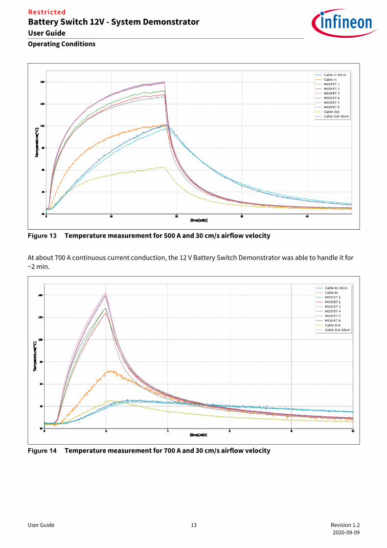
3.2 Current Carrying Capability and Thermal behaviour
The switch is designed to handle peak currents up to 1800 A. However, due to the on-state resistance of the battery switch (160 uΩ typ. at 120°C) high currents will lead to significant power dissipation and a temperature increase in the MOSFETs. The chip can handle a maximum junction temperature of 175°C. Therefore, the maximum allowable duration for high currents is limited depending on the cooling conditions. The values in
Table 6 are measured for the board exposed to a small air flow velocity of approximately 30 cm/s. and a start
temperature of 25°C.
Table 6 Current Carrying Capability Estimation @ 25°C Ambient Temperature, 70 mm² Cables
Current Power Dissipation Duration
300 A ~ 15 W Continuous
500 A ~ 40 W ~ 15 min.
700 A ~ 80 W ~ 2 min.
The thermal measurement setup can be found in Figure 10 and Figure 11. The package temperature of each switching MOSFET was measured with a thermocouple. Also, the input and output terminals, as well as the
temperatures of the cables, in distance of 40 cm were measured. This was done to estimate the rate of heat flow, which can be used as a starting point for thermal simulations.
Figure 10 Temperature measurement setup
Note: Values shown in this chapter are measured under lab conditions and will vary for different cooling setups.

User Guide 12 Revision 1.2
2020-09-09
Battery Switch 12V - System Demonstrator User Guide
Operating Conditions
Restricted
Figure 11 Temperature measurement setup
Results of the thermal measurments can be found in Figure 12 to Figure 14. For 300 A continuous current conduction MOSFET 3 to MOSFET 5 have around 58°C on top of the mold compound after 27 min of continuous conduction, see Figure 12 for detailed information.
Figure 12 Temperature measurement for 300 A and 30 cm/s airflow velocity
Figure 13 is showing the results for 500 A continuous current conduction. The inner MOSFETs are passing the 140°C after 17 min, at that time the current conduction was stopped to prevent the switch from overheating.
MOSFET 1 MOSFET 2 MOSFET 3 MOSFET 4 MOSFET 5 MOSFET 6
Cable In
Cable Out
Airflow
User Guide 13 Revision 1.2
2020-09-09
Battery Switch 12V - System Demonstrator User Guide
Operating Conditions
Restricted
Figure 13 Temperature measurement for 500 A and 30 cm/s airflow velocity
At about 700 A continuous current conduction, the 12 V Battery Switch Demonstrator was able to handle it for ~2 min.
Figure 14 Temperature measurement for 700 A and 30 cm/s airflow velocity

User Guide 14 Revision 1.2
2020-09-09
Battery Switch 12V - System Demonstrator User Guide
Switching Behaviour
Restricted
4 Switching Behaviour
4.1 Setup
In contrast to relays, MOSFETs are switching much faster and cleaner. There is no bouncing of contacts and no arcing. Switching just takes microseconds instead of several milliseconds. This is a big advantage because short circuits can be switched of before high currents are flowing through the electrical system.
For the test setup, a battery voltage of 12 V and a LLOAD of 6 µH was used. To create a short circuit, a separated MOSFET-Switch was used as RLOAD which got triggered by the output 1 of an arbitrary waveform generator (AWG), Output 1 AWG. The Signal Output 2 AWG triggers the 12 V Battery Switch Demonstrator and therefore breaks
the circuit. Both control signals where referenced to the star point of the ground connection of the system. With
the Delay between Output 1 AWG and Output 2 AWG the maximum switch off circuit current can be set.
Note: The Battery Switch 12V System Demonstrator has no overload, overcurrent or overtemperature detection implemented, a high switch off energy could destroy the MOSFETs. It is recommended to stay inside the SOA of the MOSFETs [2]. The switch off energy is dependent on the switch off current
and the intrinsic resistances and inductances of the power distribution network.
Figure 15 Measured Voltages and Currents
Figure 15 explains where the measurement probes are connected in the setup.The following waveforms in Figure
16 show the switching behaviour of the Battery Switch 12V System Demonstrator with the AUIR3242S driver. [3]
V switch
V out
V Bat
I switch out
I Bat out
I FW

User Guide 15 Revision 1.2
2020-09-09
Battery Switch 12V - System Demonstrator User Guide
Switching Behaviour
Restricted
Figure 16 Switch Timing – On and Off 4 ms horizontal timespan
4.2 Basic switching behaviour
Please note that V switch shows the drain source voltage across the MOSFETs, so a small voltage means the
switch is on (conducting) and a high voltage means the switch is off (blocking).
The delay between the occurrence of the short (Rise of Output 1 AWG) and the break of the circuit (Rise of Output
2 AWG) is responsible for the rise of the current going through the Switch. As soon as the short of the circuit
occurs, the rise of the current can be approximated by the step-response of a RL-Network.
𝑖𝐿(𝑡) =𝑈𝐵𝑎𝑡
𝑅𝑖+𝑅𝐿𝑜𝑎𝑑(1 − ⅇ−
𝑡
𝜏) with 𝜏 =𝐿𝑖+𝐿𝐿𝑜𝑎𝑑
𝑅𝑖+𝑅𝐿𝑜𝑎𝑑
Equation 1
As you can see in Figure 16 the Battery Switch 12V System Demonstrator was blocked at about 900 A. The
maximum current going through the switch is limited to 𝑖𝑚𝑎𝑥 =𝑈𝐵𝑎𝑡
𝑅𝑖+𝑅𝐿𝑜𝑎𝑑. For this specific system configuration
(RLOAD, LLOAD) it takes approximately 3.5 ms for the 900 A to reduce to zero.
The delay between the input signal Output 2 AWG and the 12 V Battery Switch Demonstrator actually breaking the circuit is caused by the input circuitry (~9 µs), see Figure 17.
When the 12 V Battery Switch Demonstrator switches off, the current delivered by the Battery (I Bat out) decreases rapidly. Therefore, the current going through the freewheeling diodes (I FW) increases, as LLOAD keeps pushing current through the electrical system. The rise of I FW is almost identical to the fall of I Bat out and only limited by the parasitic inductance and resistance between the “Batt-“terminal of the 12 V Battery Switch Demonstrator and the negativ terminal of the battery. As a result, I switch out decreases slightly faster during
the switching process as shown in Figure 17. Afterwards I switch out decreases the same way as I FW does.

User Guide 16 Revision 1.2
2020-09-09
Battery Switch 12V - System Demonstrator User Guide
Switching Behaviour
Restricted
Figure 17 Switch Timing – On and Off 200 µs timespan
Figure 17 shows that after triggering the switch V out reaches about -13 V due to the inductance of the load LLOAD. When the current flow through LLOAD is interrupted it induces a voltage that pulls V out below ground potential.
The same happens to V Bat with the induced voltage across Li pulling V Bat to about 30 V. As a result, the voltage
across the 12 V Battery Switch Demonstrator (V switch) rises to 43 V.
The energy stored in LLOAD is released by the MOSFET used as active free wheeling diode. Energy stored in Li gets released by the avalanche breakdown of the six MOSFETs. This happens when V switch reaches the avalanche
breakdown voltage of the MOSFETs, which is about (1.2 … 1.5) x VBRDSS. VBRDSS is the drain-source breakdown voltage of the MOSFET [1]. In this case the VBRDSS is between 48 V and 60 V respectively, which is higher than the
measured voltage of 43 V. An explanation for that can be found in Figure 18. V switch was measured between input terminal “Batt+” and output terminal “Out+”, during the switch off event the internal PCB Inductances are
working against the VBRDSS. If it is measured directly at the MOSFET Terminal VBRDSS of ~49 V can be seen.
Figure 18 Parasitic switch inductaces are lowering the measured V switch voltage.
I switch out decreases slightly
faster during switching process
During Avalanche and Freewheeling V out is becoming negative
Avalanche
~9µs delay
User Guide 17 Revision 1.2
2020-09-09
Battery Switch 12V - System Demonstrator User Guide
Switching Behaviour
Restricted
4.3 Approximation of avalanche losses
The avalanche of the MOSFETs occurs when the 12 V Battery Switch Demonstrator breaks the circuit and Li keeps pushing the current trought the switch and therefore the voltage across Li rises and exceeds the breakdown voltage VBRDSS. As V Switch stays almost constant during avalanche and the rise- and fall-time is negligible relative to the length of the pulse, V Switch can be described as a simple voltage pulse. Therefore, the circuitry during
the avalanche can be approximated as shown in Figure 19.
Figure 19 Approximated circuitry during avalanche breakdown
The clamping voltage of DAV is the avalanche breakdown voltage (VAV) of the switching MOSFETs. VAV can be
assumed as 1.3 x VBRDSS. However, for all the latest OptiMOSTM families VDS spikes during avalanche will not exceed 1.2 x VBRDSS [1]. As the diode clamps the voltage to VAV during avalanche we can, in first approximation, replace the
diode with a constant voltage source and get a linear differential system. By solving the differential equation, we
get the current as a function of time.
𝑖(𝑡) = ⅇ−
𝑡𝜏𝐵𝑎𝑡 (𝐼0 −
𝑉𝐵𝑎𝑡 − 𝑉𝐴𝑉
𝑅𝑖) +
𝑉𝐵𝑎𝑡 − 𝑉𝐴𝑉
𝑅𝑖
Equation 2
To obtain the avalanche breakdown losses we subtract the energy losses of the resistor from the total stored
energy (Equation 3).
𝐸𝐴𝑉 = 𝐸𝑇𝑜𝑡𝑎𝑙 − 𝐸𝑅 = 𝐿𝑖 ∙ 𝐼02 ∙ (
1
2∙
𝑉𝐴𝑉
𝑉𝐴𝑉 − 𝑉𝐵𝑎𝑡−
1
3∙ ln (1 −
𝑅𝑖 ∙ 𝐼0
𝑉𝐵𝑎𝑡 − 𝑉𝐴𝑉))
Equation 3
Note: The given equations above are only a rough approximation and should only be used for a first
estimation.
User Guide 18 Revision 1.2
2020-09-09
Battery Switch 12V - System Demonstrator User Guide
Switching Behaviour
Restricted
4.3.1 Example calculation for the Battery Switch 12V System Demonstrator
As example calculation the initial avalanche current I0= 900 A, the internal battery resistance Ri=5 mΩ and the internal inductance Li=100 nH can be used. VAV is approximately 1.2* VBRDSS, where VBRDSS = 40 V for the IPLU300N04S4-R8. By using Equation 3 we can estimate the avalanche energy.
𝐸𝐴𝑉 = 𝐸𝑇𝑜𝑡𝑎𝑙 − 𝐸𝑅 = 100𝑛𝐻 ∙ (900𝐴)2 ∙ (1
2∙
48𝑉
48𝑉 − 12𝑉−
1
3∙ ln (1 −
5𝑚Ω ∙ 900𝐴
12𝑉 − 48𝑉)) = 50,8𝑚𝐽
Equation 4
When assumed that the complete avalanche energy is absorbed by all six MOSFETs equally, the maximum
avalanche energy can be extrapolated from the avalanche energy graph of the datasheet [2] and multiplied by six, for six parallelized MOSFETs.
Note: Due to the production distribution of VBRDSS and temperature differences of the MOSFET dies the avalanche energy may not be spread equaly among all MOSFETs.
4.3.2 Simulated Safe Operating Areas at different Battery Configurations
Equation 3 shows that the avalanche energy is a function of the internal resistance, inductance of the battery, the battery voltage, the avalanche breakdownvoltage of the MOSFETs and the current going through the 12 V Battery Switch Demonstrator. As these parameters are different in every application, it is not possible to estimate
a single absolute maximum rating. Different battery configurations need to be considered. Additionally, the
limits for the maximum avalanche energy are strongly dependend on the junction temperature of the MOSFETs.
Therefore, multiple safe operating area plots based on simulation results are provided below. The simulations
are done for lab conditions, at 25°C junction temperature.
Note: The results below are restricted to lab conditions. It is recommended to stay inside the SOA of the MOSFET [2]. For additional information or help with your specific application, please get in contact
with Infineon Technologies AG.
Figure 20 SOA for 12 V, Current = 1500 A, Limit = 6*500mJ, Tj=25°C, limit extracted from Datasheet [2]
UNSAFE AREA
SAFETY MARGIN
SAFE AREA

User Guide 19 Revision 1.2
2020-09-09
Battery Switch 12V - System Demonstrator User Guide
Switching Behaviour
Restricted
Figure 21 SOA for 12 V, Current = 1800 A, Limit = 6*380mJ, Tj=25°C, limit extracted from Datasheet [2]
UNSAFE AREA
SAFETY MARGIN
SAFE AREA

User Guide 20 Revision 1.2
2020-09-09
Battery Switch 12V - System Demonstrator User Guide
Mechanical Dimensions
Restricted
5 Mechanical Dimensions
Figure 22 Board Dimensions [mm]
Figure 23 PCB Holder [mm]

User Guide 21 Revision 1.2
2020-09-09
Battery Switch 12V - System Demonstrator User Guide
Schematics
Restricted
6 Schematics
Figure 24 Top Level Schematics

User Guide 22 Revision 1.2
2020-09-09
Battery Switch 12V - System Demonstrator User Guide
Schematics
Restricted
Figure 25 MOSFET Driver Circuit

User Guide 23 Revision 1.2
2020-09-09
Battery Switch 12V - System Demonstrator User Guide
Schematics
Restricted
Figure 26 Input Circuitry

User Guide 24 Revision 1.2
2020-09-09
Battery Switch 12V - System Demonstrator User Guide
Schematics
Restricted
Figure 27 Active Freewheeling Circuitry
User Guide 25 Revision 1.2
2020-09-09
Battery Switch 12V - System Demonstrator User Guide
Schematics
Restricted
Figure 28 Power Stage

User Guide 26 Revision 1.2
2020-09-09
Battery Switch 12V - System Demonstrator User Guide
PCB Description
Restricted
7 PCB Description
7.1 PCB Technology
The Printed Circuit Board used for the shown Battery Switch 12V System Demonstrator is a product idea of Schweizer Electronic AG. The deployment of the Inlay Board 2.0 technology assures highest current carrying capability in conjunction with lowest thermal resistance. A superior thermal connection between the MOSFETs
and the integrated power rail of the PCB allows to conduct a permanent current of up to 300A and a short-circuit current of up to 1800A. The complete feature set is visible in Table 7.
Table 7 Feature Set of Metal Core Board (Non-Isolated Version)
Feature Value
Size 100.0 mm x 57.0 mm
Thickness 1.3 mm
Electrical resistance 60 µΩ
Thermal resistance (non-isolated version) 0.1 K/W
Thermal resistance (isolated version) ~ 0.2 K/W
No. of copper-filled laser vias per MOSFET 300
Figure 29 PCB Stackup
The PCB Stackup is shown in Figure 29. The core of the PCB is a copper plate of 1.0 mm thickness which represents the power rail for the 12 V Battery Switch Demonstrator. This copper plate is structured by an isolation
gap of 500 µm width. By means of a lamination process the isolation gap is filled with the resin from Prepreg
material. This represents a safe isolation space between battery and load potential. The outer layers are consisting of 35 µm copper foils, after plating 70 µm. To ensure both a low-ohmic electrical connection from the MOSFETs to the current rail and a good heat flow to a potentially used heatsink, the PCB is provided with
hundreds of copper-filled microvias in the soldering area of the MOSFET and on the back-side of the PCB. The high filling factor with dimple depths lower than 25 µm allows the designer to have the MOSFETs soldered on top of the via field without facing the risk of solder voids. During assembly it has to be made sure that solder profiles will be used which are appropriate for power PCBs with a large thermal mass. The MOSFETs are placed on the
PCB so that the MOSFETs, once they are turned on, connect the two isolated parts of the PCB, see cross section
in Figure 30.

User Guide 27 Revision 1.2
2020-09-09
Battery Switch 12V - System Demonstrator User Guide
PCB Description
Restricted
Figure 30 Cross Section
For higher logic content requirements, the Inlay Board 2.0 technology can optionally accommodate an area with four or more electrical layers next to the power rails as demonstrated with the 12 V Battery Switch Demonstrator.
7.2 PCB Layout
Figure 31 Top Layer

User Guide 28 Revision 1.2
2020-09-09
Battery Switch 12V - System Demonstrator User Guide
PCB Description
Restricted
Figure 32 Logic Ground Layer
Figure 33 Power Layer

User Guide 29 Revision 1.2
2020-09-09
Battery Switch 12V - System Demonstrator User Guide
PCB Description
Restricted
Figure 34 1mm Inlay-Design from Schweizer Electronic AG
Figure 35 Bottom Layer

User Guide 30 Revision 1.2
2020-09-09
Battery Switch 12V - System Demonstrator User Guide
Bill Of Materials
Restricted
8 Bill Of Materials
Table 8 12V Variant
Designator Value Description
C1, C5 220nF/50V Capacitor 0805 X7R 10%
C2 100nF/100V Capacitor 0805 X7R 10%
C3, C9, C13 1uF/25V Capacitor 0603 X7R 10%
C4, C8, C11 100nF/50V Capacitor 0603 X7R 10%
C6 1uF/50V Capacitor 1206 X7R 10%
C7 4.7uF/35V Capacitor 0805 X7S 10%
D1 1N4148W-13-F Standard Diode
D2, D8 GDZ18B-G3-08 Zener Diode, 18V, 200mW
D3 SZ1SMA5931BT3 Zener Diode, 18V, 1.5W
D5 BZX84C5V1LT1G Zener Diode, 5.1V, 250mW
D9, D10, D11, D12, D13, D14
MM5Z18VT1G Zener Diode, 18V, 200mW
G1 TLS810A1LD V50 Ultra Low Quiescent Linear Voltage Regulator, 5V
L1 LPS6235-474MR Shielded Power Inductor, 470uH
Q1, Q2, Q3, Q4, Q5, Q6, Q7, Q8
IPLU300N04S4-R8 OptiMOS T2 N-Channel Enhancement Power-Transistor, 40 V
Q9, Q14 NSV1C200LT1G 100V, 2.0 A, Low VCEsat PNP Transistor
Q10, Q15 BSS138N N-Channel Small Signal Transistor
R1 680R Resistor 0603 75V 1%
R2, R3, R4, R6 120k Resistor 0603 75V 1%
R5 100R Resistor 0603 75V 1%
R7, R25 1R Resistor 0805 150V 1%
R8 4.7k Resistor 0603 75V 1%
R9, R11, R28 10k Resistor 0603 75V 1%
R10, R23, R24, R29, R30, R33
2.2R Resistor 0603 75V 1%
R12 12R Resistor 0603 75V 1%
R13 100k Resistor 0603 75V 1%
R15, R16, R31, R32 3.3k Resistor 0603 75V 1%
R17, R18, R19, R20, R21, R22
8.2R Resistor 0603 75V 1%
R26 5.1k Resistor 0603 75V 1%
R35/D6 0R/Jumper Resistor 1206
U1 LT6015IS5 Low Power Op Amp
U2 AUIR3242S Low Quiescent Current Back to Back MOSFET Driver
U4 74LVC2G74 Positive Edge Triggered D-Type Flip Flop
X1 TSM-102-01-S-SV SMT .025'' SQ Post Header, 2.54mm Pitch, 2 Pin, Vertical, Single Row
X2 TSM-103-01-L-DV SMT .025'' SQ Post Header, 2.54mm Pitch, 6 Pins, Vertical, Double Row

User Guide 31 Revision 1.2
2020-09-09
Battery Switch 12V - System Demonstrator User Guide
References
Restricted
9 References
[1] Some key facts about avalanche - Infineon Technologies AG, Version 1.0, 2017-01-9
[2] IPLU300N04S4-R8 datasheet - Infineon Technologies AG, Rev. 1.0, 2015-10-06
[3] AUIR3242S datasheet - Infineon Technologies AG, Rev. 1.0, 2018-07-26

User Guide 32 Revision 1.2
2020-09-09
Battery Switch 12V - System Demonstrator User Guide
Revision History
Revision History
Major changes since revision 1.1
Page or Reference Description of change
Updated filename and demonstrator nomenclature
Major changes since revision 1.0
Page or Reference Description of change
Page 4 Added some more details to Figure 3
Page 6 Clarify descriptions of connector X1 and X2
Page 15 Added Figure 18 to explain the switching event in more detail

Trademarks of Infineon Technologies AG µHVIC™, µIPM™, µPFC™, AU-ConvertIR™, AURIX™, C166™, CanPAK™, CIPOS™, CIPURSE™, CoolDP™, CoolGaN™, COOLiR™, CoolMOS™, CoolSET™, CoolSiC™, DAVE™, DI-POL™, DirectFET™, DrBlade™, EasyPIM™, EconoBRIDGE™, EconoDUAL™, EconoPACK™, EconoPIM™, EiceDRIVER™, eupec™, FCOS™, GaNpowIR™, HEXFET™, HITFET™, HybridPACK™, iMOTION™, IRAM™, ISOFACE™, IsoPACK™, LEDrivIR™, LITIX™, MIPAQ™, ModSTACK™, my-d™, NovalithIC™, OPTIGA™, OptiMOS™, ORIGA™, PowIRaudio™, PowIRStage™, PrimePACK™, PrimeSTACK™, PROFET™, PRO-SIL™, RASIC™, REAL3™, SmartLEWIS™, SOLID FLASH™, SPOC™, StrongIRFET™, SupIRBuck™, TEMPFET™, TRENCHSTOP™, TriCore™, UHVIC™, XHP™, XMC™ Trademarks updated November 2015
Other Trademarks All referenced product or service names and trademarks are the property of their respective owners. ifx1owners.
Edition 2020-09-09
Published by
Infineon Technologies AG
81726 Munich, Germany
© 2020 Infineon Technologies AG.
All Rights Reserved.
IMPORTANT NOTICE The information contained in this application note is given as a hint for the implementation of the product only and shall in no event be regarded as a description or warranty of a certain functionality, condition or quality of the product. Before implementation of the product, the recipient of this application note must verify any function and other technical information given herein in the real application. Infineon Technologies hereby disclaims any and all warranties and liabilities of any kind (including without limitation warranties of non-infringement of intellectual property rights of any third party) with respect to any and all information given in this application note. The data contained in this document is exclusively intended for technically trained staff. It is the responsibility of customer’s technical departments to evaluate the suitability of the product for the intended application and the completeness of the product information given in this document with respect to such application.
For further information on the product, technology, delivery terms and conditions and prices please contact your nearest Infineon Technologies office (www.infineon.com).
WARNINGS Due to technical requirements products may contain dangerous substances. For information on the types in question please contact your nearest Infineon Technologies office. Except as otherwise explicitly approved by Infineon Technologies in a written document signed by authorized representatives of Infineon Technologies, Infineon Technologies’ products may not be used in any applications where a failure of the product or any consequences of the use thereof can reasonably be expected to result in personal injury.