Based on the gm=ID Ratio for Nanometerdigital.csic.es/bitstream/10261/83306/4/lc_vco.pdf1 LC-VCO...
25
1 LC-VCO Design Optimization Methodology Based on the g m /I D Ratio for Nanometer CMOS Technologies Rafaella Fiorelli, Eduardo Peral´ ıas and Fernando Silveira, Abstract In this paper, an LC-VCO design optimization methodology based on the g m /I D technique and on the exploration of all inversion regions of the MOS transistor is presented. An in-depth study of the compromises between phase noise and current consumption permits optimization of the design for given specifications. Semi-empirical models of MOS transistors and inductors, obtained by simulation, jointly with analytical phase noise models, allow to get a design space map where the design trade-offs are easily identified. Four LC-VCO designs in different inversion regions in a 90 nm CMOS process are obtained with the proposed methodology and verified with electrical simulations. Finally, the implementation and measurements are presented for a 2.4 GHz VCO operating in moderate inversion. The designed VCO draws 440 μA from a 1.2V power supply and presents a phase noise of -106.2 dBc/Hz at 400 kHz from the carrier. I. I NTRODUCTION The increasing demand of wireless applications with special emphasis on low power requirements forces radio-frequency designers to work at the limits of the technology. To achieve these challeng- ing specifications, best performance is mandatory in each block of the circuit, especially in terms of power consumption, noise and linearity. In addition, since a few years ago, the extended use of CMOS technologies enables RF designers to reduce costs as well as reaching good performance. Rafaella Fiorelli and Eduardo Peral´ ıas are with the Instituto de Microelectr´ onica de Sevilla, CNM-CSIC, Seville, 41092, Spain (e-mail:fi[email protected], [email protected]). Fernando Silveira is with the Instituto de Ingenier´ ıa Elctrica, Universidad de la Rep´ ublica, Montevideo, 11300, Uruguay (e-mail:silveira@fing.edu.uy). October 29, 2013 DRAFT
Transcript of Based on the gm=ID Ratio for Nanometerdigital.csic.es/bitstream/10261/83306/4/lc_vco.pdf1 LC-VCO...

1
LC-VCO Design Optimization Methodology
Based on the gm/ID Ratio for Nanometer
CMOS TechnologiesRafaella Fiorelli, Eduardo Peralıas and Fernando Silveira,
Abstract
In this paper, an LC-VCO design optimization methodology based on the gm/ID technique and on
the exploration of all inversion regions of the MOS transistor is presented. An in-depth study of the
compromises between phase noise and current consumption permits optimization of the design for given
specifications. Semi-empirical models of MOS transistors and inductors, obtained by simulation, jointly
with analytical phase noise models, allow to get a design space map where the design trade-offs are
easily identified.
Four LC-VCO designs in different inversion regions in a 90 nm CMOS process are obtained with
the proposed methodology and verified with electrical simulations. Finally, the implementation and
measurements are presented for a 2.4 GHz VCO operating in moderate inversion. The designed VCO
draws 440 µA from a 1.2V power supply and presents a phase noise of −106.2 dBc/Hz at 400 kHz
from the carrier.
I. INTRODUCTION
The increasing demand of wireless applications with special emphasis on low power requirements
forces radio-frequency designers to work at the limits of the technology. To achieve these challeng-
ing specifications, best performance is mandatory in each block of the circuit, especially in terms of
power consumption, noise and linearity. In addition, since a few years ago, the extended use of CMOS
technologies enables RF designers to reduce costs as well as reaching good performance.
Rafaella Fiorelli and Eduardo Peralıas are with the Instituto de Microelectronica de Sevilla, CNM-CSIC, Seville, 41092, Spain
(e-mail:[email protected], [email protected]).
Fernando Silveira is with the Instituto de Ingenierıa Elctrica, Universidad de la Republica, Montevideo, 11300, Uruguay
(e-mail:[email protected]).
October 29, 2013 DRAFT

2
Fig. 1. (a) gm/ID and (b) gds/ID vs. i = ID/(W/L) for four nMOS transistors and a VDS = 600 mV . Typical limits of
strong (SI), moderate (MI) and weak (WI) inversion regions are shown.
The requirements of an RF block, such as gain, noise or power consumption, strongly depend on the RF
application. For example, an application that is very demanding in terms of noise would need to accept
high power consumption, whereas a very low power design would cope with just enough non-very-low
noise values. As these two characteristics are directly related, their trade-off has to be achieved optimizing
the design of RF blocks. This work explores those compromises in order to optimize inductor-capacitor-
tank voltage controlled oscillators (LC-VCOs). This study is relevant as VCOs, due to their phase noise,
are responsible for most part of the error in the processed signal in an RF receiver [1], as well as for
a non-negligible percentage of the system current consumption. The mentioned optimization is done by
exploiting the consumption-spectral purity trade-off of the VCOs in order to use just the needed current
to fulfill the application requirements. This is achieved by using the ratio of transconductance to drain
current gm/ID methodology presented in [2], [3] and taking advantage of operation in all the inversion
regions (weak, moderate and strong) of the MOS transistor (MOST) [4].
The gm/ID ratio of a saturated MOST is directly related to its inversion level. The inversion level
is directly associated with the normalized current or current density, defined as i = ID/(W/L) and
dependent on the gate, source and drain voltages [5]–[7]. The relationship between gm/ID and i -and
hence ID for a certain MOST aspect ratio W/L- is biunivocal; a typical form of this curve can be
October 29, 2013 DRAFT

3
appreciated in Fig. 1(a). Several factors make the gm/ID ratio a very useful parameter for describing the
state of operation and performance of a MOST and exploring its design space. Firstly, the ease to write
circuit design expressions as a function of this parameter, since generally the transconductance or the
current are part of them. Secondly, its value gives a direct indication of the inversion region and of the
efficiency of the transistor in translating current consumption into transconductance. Finally, its variation
is constrained to a very small range, efficiently covered with a grid of some tens of values of gm/ID
(e.g. from 3 V −1 to 28 V −1 for a nanometer bulk nMOS). Utilizing this variable on the expressions of
the VCO characteristics and sweeping gm/ID allows to obtain a set of design space maps of phase noise,
gain, power consumption, among others, as it will be shown in Section V. This graphical representation
helps the designer to study the evolution and trade-offs of some of these characteristics when working
in any of the three inversion regions.
The MOST channel length reduction, as it is shown below, permits the design of RF blocks in weak and
moderate inversion (WI/MI) with less power consumption than when they are biased in the traditional way,
in the strong inversion (SI) region. Several RF blocks designed in CMOS technologies and working in MI
or WI have been reported in the last decade. Porret et al. [8] and Melly et al. [9] present, respectively, the
design of a receiver and a transmitter working at 433 MHz in MI. Ramos et al. [10] showed a 950 MHz
LNA in MI-WI. The authors have presented an RF amplifier for 900 MHz [11] and a 2.4 GHz VCO [12]
both designed in MI regions. Lee and Mohammadi [13] presented a 2.4 GHz VCO design in WI whereas
Hsieh and Lu [14] designed a 5 GHz receiver front-end in MI and WI. Finally, Perumana et al. [15]
designed a subthreshold 2.4 GHz receiver. Although the mentioned works successfully take advantage of
working in these MOS regions of operation, they do not present a systematic methodology for choosing
the operating point. This issue is covered in this paper for LC-VCOs.
The effect of moving from SI through WI implies a considerable current reduction, but as a counterpart,
parasitic capacitances are higher as the transistor dimensions increase. That is why, with sub-micrometer
technologies, high frequency design in MI is limited to around one gigahertz [11]. Nowadays, the advent
of nanometer CMOS technologies prepared for radio-frequency designs enable to design in MI with
working frequencies of several gigahertz. This idea considers the conservative limit where the MOS
transistor frequency is below the quasistatic-limit frequency of one tenth of fT [4], with fT the MOST
transition frequency. To visualize these facts, fT and gm/ID versus ID are depicted in Fig. 2 for a pMOS
transistor in 90 nm technology. These results show that increasing ID (i.e. moving to SI) leads to a rise
in fT and a reduction in the gm/ID ratio. It is also appreciated in Fig. 3, where the relation between fT
and gm/ID and the overdrive voltage VOD = VGS − VT , a parameter classically utilized in RF designs
October 29, 2013 DRAFT

4
Fig. 2. gm/ID and fT versus ID of a pMOS transistor with an aspect ratio of 360 µm/100 nm.
Fig. 3. fT versus gm/ID and versus the overdrive voltage VOD for nMOS transistors.
to indicate the bias point, are depicted. These plots also show that, in spite of the considerable fall in fT
when working in MI, the resulting value is enough to work in the RF range of some gigahertz.
The proposed optimization methodology follows four steps. First of all, the DC and low frequency,
small signal behaviour of the MOS transistor has to be reflected in suitable expressions or curves of
gm/ID, gds/ID and intrinsic capacitances versus i, as it will be discussed in Section II. In second place
comes the extraction of the models for passive components, presented in Section III. In third place is the
modeling of the LC-VCO, where the expressions of phase noise (L), output voltage Vout and VCO flicker
corner frequency fc,1/f3 are reordered to make them function of gm/ID and i. This step is presented
in Section IV. Finally, a design flow is provided; it organizes the necessary computations based on the
third step and the decisions constrained by the VCO specifications, while it uses the technological data
October 29, 2013 DRAFT
5
collected in the first two steps. This fourth phase is developed in Section V. Sections VI and VII validate
this design methodology, contrasting four VCO designs with their correspondent electrical simulations
as well as presents measurement results of a specific implementation. Section VIII summarizes the main
contributions of this work.
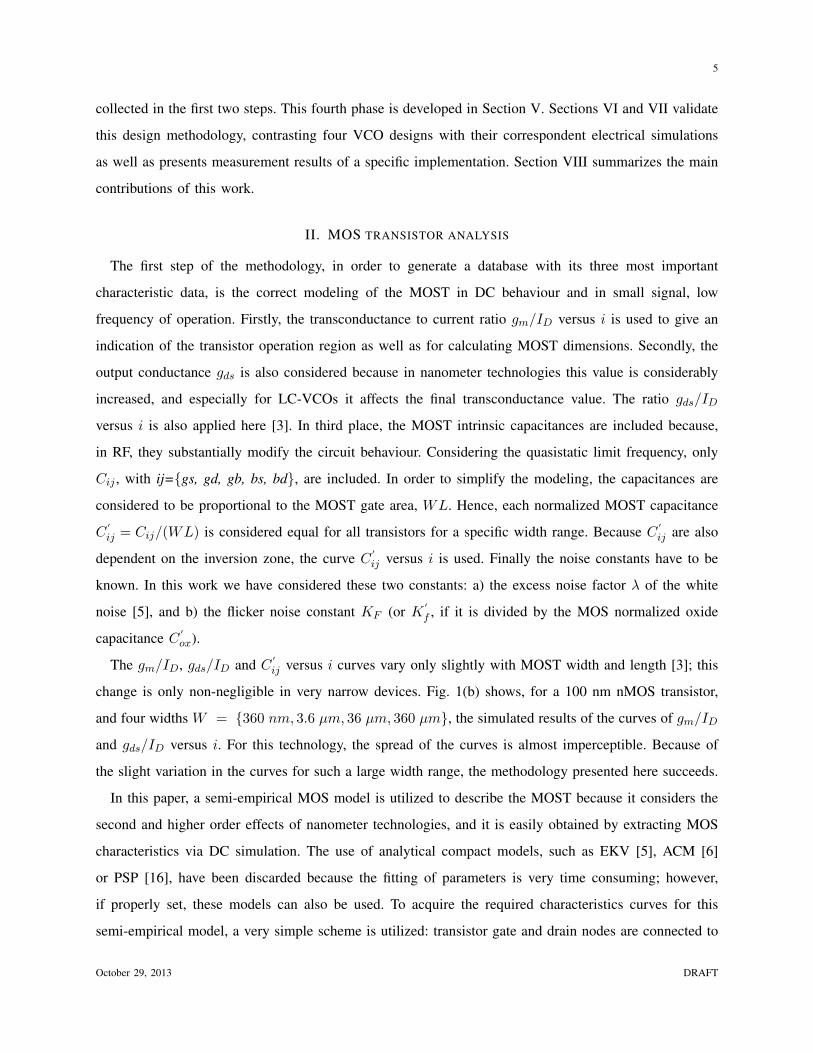
II. MOS TRANSISTOR ANALYSIS
The first step of the methodology, in order to generate a database with its three most important
characteristic data, is the correct modeling of the MOST in DC behaviour and in small signal, low
frequency of operation. Firstly, the transconductance to current ratio gm/ID versus i is used to give an
indication of the transistor operation region as well as for calculating MOST dimensions. Secondly, the
output conductance gds is also considered because in nanometer technologies this value is considerably
increased, and especially for LC-VCOs it affects the final transconductance value. The ratio gds/ID
versus i is also applied here [3]. In third place, the MOST intrinsic capacitances are included because,
in RF, they substantially modify the circuit behaviour. Considering the quasistatic limit frequency, only
Cij , with ij={gs, gd, gb, bs, bd}, are included. In order to simplify the modeling, the capacitances are
considered to be proportional to the MOST gate area, WL. Hence, each normalized MOST capacitance
C′
ij = Cij/(WL) is considered equal for all transistors for a specific width range. Because C′
ij are also
dependent on the inversion zone, the curve C′
ij versus i is used. Finally the noise constants have to be
known. In this work we have considered these two constants: a) the excess noise factor λ of the white
noise [5], and b) the flicker noise constant KF (or K′
f , if it is divided by the MOS normalized oxide
capacitance C′
ox).
The gm/ID, gds/ID and C′
ij versus i curves vary only slightly with MOST width and length [3]; this
change is only non-negligible in very narrow devices. Fig. 1(b) shows, for a 100 nm nMOS transistor,
and four widths W = {360 nm, 3.6 µm, 36 µm, 360 µm}, the simulated results of the curves of gm/ID
and gds/ID versus i. For this technology, the spread of the curves is almost imperceptible. Because of
the slight variation in the curves for such a large width range, the methodology presented here succeeds.
In this paper, a semi-empirical MOS model is utilized to describe the MOST because it considers the
second and higher order effects of nanometer technologies, and it is easily obtained by extracting MOS
characteristics via DC simulation. The use of analytical compact models, such as EKV [5], ACM [6]
or PSP [16], have been discarded because the fitting of parameters is very time consuming; however,
if properly set, these models can also be used. To acquire the required characteristics curves for this
semi-empirical model, a very simple scheme is utilized: transistor gate and drain nodes are connected to
October 29, 2013 DRAFT

6
a DC voltage source, while source and bulk nodes are connected either to ground (nMOS transistor) or to
the supply voltage (pMOS transistor). Then, the gate voltage VG is swept extracting ID, gm, gds and C′
ij .
The drain voltage is set around its expected DC value in the target circuit. To get a very complete dataset
the same simulation should be run for a set of widths (for example, the set chosen for Fig. 1), when a
fixed transistor length value is used. Otherwise, following the same idea, a small set of lengths should
be chosen. Finally, λ and KF values should be obtained from handling MOST noise data provided by
the foundry or estimated from simulations or measurements [17].
III. ANALYSIS OF PASSIVE COMPONENTS
The second step in the methodology is the characterization of passive components. LC-VCOs per-
formance is very much dependent on their non-idealities. Their characterization can be done either by
semi-empirical models of library cells provided by the foundry or by electromagnetic solvers such as
ASITIC [18] or ADSTMMomentum. Electromagnetic solver has major drawbacks: 1) the need to have the
technological data provided by the foundry to obtain accurate descriptions, and 2) the high computational
time spent to obtain the solutions.
In this paper, for the sake of efficiency, we utilize passive element cells supplied by the foundry. By
means of S-parameter analysis, we obtain their equivalent complex admittance at the working frequency,
f0.
A. Inductor modeling
In this work, the differential tank inductor is modeled at the oscillation frequency as a network of
an equivalent inductor Lind and a parallel parasitic resistor Rind. S-parameter analysis is applied to
extract the parameters of the model with the inductor in a differential configuration. In order to obtain
a complete database, the analysis has to be done for a large set of inductors. In this work, the best
inductor is considered the one with the highest parallel resistance, since it will lead to the lowest required
transconductance and hence consumption, as it will be shown in Section IV. Looking for biunivocal
relationships between Lind and Rind, computational routines are implemented to find, for a particular
inductance value, the nearest best inductor. Figure 4 displays the resulting Rind of sweeping coil conductor
width for our standard 90 nm CMOS process and highlights the inductors dataset with the maximum
resistances. The data in this plot show that the highest resistances come with the largest inductance values.
October 29, 2013 DRAFT

7
Fig. 4. Parallel resistance versus inductance value Lind for four inductor widths w with a common external diameter of
300 µm, at f0=2.4 GHz. The black line represents the inductors with the highest resistance.
B. Varactor modeling
Varactor parasitic resistance has been usually neglected, especially due to its high value compared with
inductor parasitic resistance. However, on-chip coils have improved and it is possible to have a varactor
conductance comparable with inductor conductance. Therefore, varactor parasitic resistance extraction by
simulations is now necessary, in order to check whether it must be considered in the design.
For the accumulation nMOS varactors used in the design presented in Section VI, the maximum value
of gvar over the varactor control voltage range is approximately 70 µS; so varactor conductance can be
ignored compared to the conductances of the other VCO components.
IV. VCO MODELING
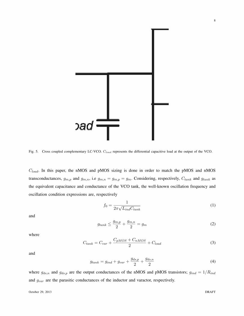
The LC-VCO topology used in this work is depicted in Fig. 5. It shows a cross-coupled complementary
VCO with its LC tank, biased with a pMOS current mirror, which drives the Ibias current to the LC-
VCO. This pMOS structure is used for its better flicker noise performance with respect to an nMOS one
with the same size. Cross-coupled transistors provide the needed negative feedback and a pMOS-nMOS
complementary structure increases VCO transconductance while consuming the same quiescent drain
current, ID, with Ibias = 2 · ID.
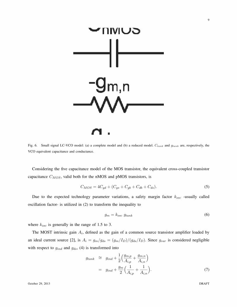
A small-signal model of the LC-VCO of Fig. 5 is displayed in Fig. 6(a) jointly with its simplified
model in Fig. 6(b). It comprises the equivalent inductance of the differential inductor Lind and the
equivalent capacitance of the varactors Cvar, both calculated at the oscillation frequency f0; the equivalent
parasitic capacitances of the nMOS and pMOS transistors CnMOS and CpMOS ; and the load capacitance
October 29, 2013 DRAFT
8
Fig. 5. Cross coupled complementary LC-VCO. Cload represents the differential capacitive load at the output of the VCO.
Cload. In this paper, the nMOS and pMOS sizing is done in order to match the pMOS and nMOS
transconductances, gm,p and gm,n, i.e gm,n = gm,p = gm. Considering, respectively, Ctank and gtank as
the equivalent capacitance and conductance of the VCO tank, the well-known oscillation frequency and
oscillation condition expressions are, respectively
f0 =1
2π√LindCtank
(1)
and
gtank ≤gm,p
2+gm,n
2= gm (2)
where
Ctank = Cvar +CpMOS + CnMOS
2+ Cload (3)
and
gtank = gind + gvar +gds,p
2+gds,n
2(4)
where gds,n and gds,p are the output conductances of the nMOS and pMOS transistors; gind = 1/Rind
and gvar are the parasitic conductances of the inductor and varactor, respectively.
October 29, 2013 DRAFT
9
Fig. 6. Small signal LC-VCO model: (a) a complete model and (b) a reduced model. Ctank and gtank are, respectively, the
VCO equivalent capacitance and conductance.
Considering the five capacitance model of the MOS transistor, the equivalent cross-coupled transistor
capacitance CMOS , valid both for the nMOS and pMOS transistors, is
CMOS = 4Cgd + (Cgs + Cgb + Cdb + Cds). (5)
Due to the expected technology parameter variations, a safety margin factor kosc -usually called
oscillation factor- is utilized in (2) to transform the inequality to
gm = kosc gtank (6)
where kosc is generally in the range of 1.5 to 3.
The MOST intrinsic gain Ai, defined as the gain of a common source transistor amplifier loaded by
an ideal current source [2], is Ai = gm/gds = (gm/ID)/(gds/ID). Since gvar is considered negligible
with respect to gind and gds, (4) is transformed into
gtank ∼= gind +12
(gm,pAi,p
+gm,nAi,n
)= gind +
gm2
( 1Ai,p
+1Ai,n
). (7)
October 29, 2013 DRAFT

10
Using (6)
gind = gm
( 1kosc− 1
2Ai,p− 1
2Ai,n
)=
gmk′osc
. (8)
Then, gm results finally in
gm = k′
osc gind. (9)
The differential output voltage of the tank Vout is estimated as in [19]
Vout = V0+ − V0− ∼=4π
2IDgtank
=8π
k′
osc
gm/ID. (10)
A. Phase noise model
Phase noise L is a fundamental characteristic of a VCO that describes its spectral purity around its
oscillation frequency f0 [20]. Considering a frequency offset ∆f around f0, three asymptotic zones can
be defined [21]. Very near f0, L decreases proportionally to 1/f3 and it is directly related to the flicker
noise of MOS transistors. Then, a spectrum zone inversely proportional to f2 appears, mainly caused
by the white noise of VCO elements. Finally, far from f0, there is a flat zone, the VCO floor noise,
where the external noise sources dominate. Generally it is the 1/f2 zone where the VCO phase noise is
specified. The asymptotic limits of the three regions can be found making equal the expressions for two
adjacent zones and solving for f . Particularly, the flicker corner frequency fc,1/f3 is the VCO parameter
that defines the lower limit of the 1/f2 zone.
To visualize and fully exploit the phase noise-current consumption trade-off, an analytical model for
phase noise valid for all the inversion regions is used in this work by means of expressing the phase
noise equations as functions of the gm/ID ratio. The initial expressions of this phase noise model were
presented by Hajimiri in [20]. This is a linear time variant model, with compact equations, very suitable
for our methodology. In the 1/f2 region of the spectrum (see Appendix A for derivation) the phase noise
expression is
L1/f2(∆f) = 10log(kBT
π2
641Q2
gmID
1ID
f20
∆f2λ)
(11)
where λ = γαeq
+ 1kosc
, γ is the excess noise factor, kB is the Boltzmann constant, T is the absolute
temperature, f0 is the oscillation frequency, ∆f is the frequency offset and αeq is defined as
αeq =(gd0,n
gm,n+gd0,p
gm,p
)−1(12)
with gd0,n and gd0,p the zero-bias (i.e VDS = 0) drain conductances gds, for nMOS and pMOS respectively.
Tank quality factor, Q, is calculated as
Q =1
2πf0Lindgtank. (13)
October 29, 2013 DRAFT
11
Similarly, we derive a phase noise expression for the 1/f3 zone (see Appendix B for derivation):
L1/f3(∆f) = 10 log
(Γ2av
8π2
64
(K
′
F,n
WnL+K
′
F,p
WpL
)1Q2
(gmID
)2 f20
∆f3
)(14)
where K′
F,n and K′
F,p are the nMOS and pMOS normalized flicker noise constants, and Γav is the average
value of the impulse sensitivity function Γ defined in [20].
The LC-VCO flicker corner frequency fc,1/f3 is expressed as a function of the transistor corner
frequency fc. It is approximately (see Appendix D):
fc,1/f3 = k0fc,eq ∼= k0KFαeq4kBTγ
gmIDi
1L2
(15)
where k0 and f1/c,eq are defined in Appendix D.
The data obtained from previously designed LC-VCO allow us to estimate the Γav coefficient on which
k0 depends. For these circuits, Γav ≤ 0.4 and k0 ≤ 0.16. It means that fc,1/f3 is generally much smaller
than fc. Γav is dramatically reduced if the VCO layout is highly symmetrical [20] and if the output signal
is a low distorted sinusoidal waveform.
The equations formulated before, particularly (11) and (14), help us to quantitatively visualize the
compromises between phase noise and current consumption. Considering a fixed gm, imposed by (9),
when gm/ID rises, i.e when moving towards weak inversion, ID decreases in the same proportion. Rising
gm/ID and reducing ID leads to a phase noise increment in the 1/f2 and 1/f3 spectrum regions. The
design methodology, presented in the following section, explores these trade-offs, making it possible to
optimize consumption while achieving the specified phase noise level.
V. PROPOSED DESIGN METHODOLOGY
The methodology proposed hereafter intends to give a simple way to size the LC-VCO components
and to visualize graphically the trade-offs inherent in the design. The flow diagram of the method is
represented in Fig. 7, and it is organized in the following steps:
Step 1: Start fixing a set of initial parameters and limits: minimum transistor channel length Lmin, safety
margin factor kosc, maximum equivalent inductance Lind,max, minimum varactor capacitance Cvar,min
and Cload. Next, set the VCO specifications: oscillation frequency f0, maximum current ID,max, maximum
phase noise in the white noise zone L1/f2,max at an offset ∆f and minimum output voltage Vout,min.
Step 2: Pick a pair of values of inductor Lind and gm/ID ratio, from the technological database of
inductors and transistors, which is assumed previously collected.
October 29, 2013 DRAFT
12
Fig. 7. Flow diagram of the proposed VCO design methodology.
Step 3: From the inductor database, derive the gind of that inductor. Obtain the normalized currents of
nMOS and pMOS, in and ip, as well as gds/ID, from the picked gm/ID and the characteristic curves
(gm/ID vs. i) and (gds/ID vs. i). Calculate the intrinsic gains Ai,n and Ai,p and then deduce k′
osc. Extract
the transistors equivalent capacitance from C′
nMOS vs. i and C′
pMOS vs. i tables.
Step 4: Deduce gm from (9). With gm and gm/ID calculate the drain current ID, and with (10) compute
Vout. Then, calculate the transistors widths Wn and Wp from ID and in and ip and compute CnMOS and
October 29, 2013 DRAFT
13
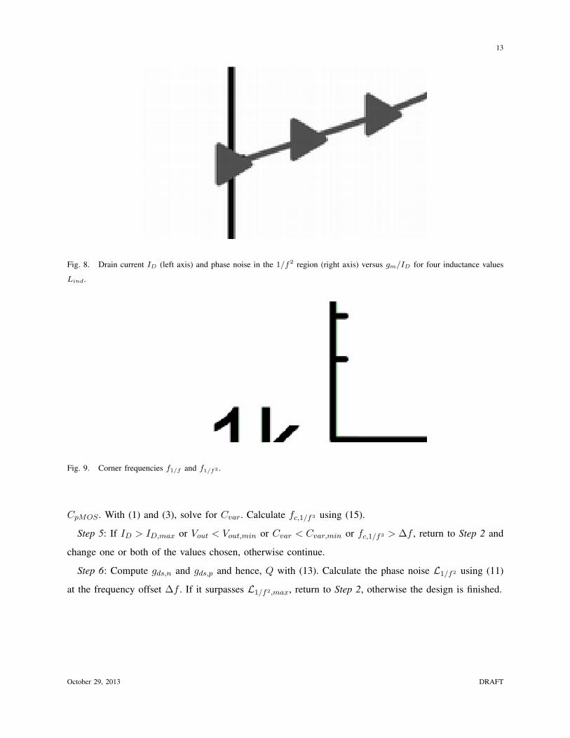
Fig. 8. Drain current ID (left axis) and phase noise in the 1/f2 region (right axis) versus gm/ID for four inductance values
Lind.
Fig. 9. Corner frequencies f1/f and f1/f3 .
CpMOS . With (1) and (3), solve for Cvar. Calculate fc,1/f3 using (15).
Step 5: If ID > ID,max or Vout < Vout,min or Cvar < Cvar,min or fc,1/f3 > ∆f , return to Step 2 and
change one or both of the values chosen, otherwise continue.
Step 6: Compute gds,n and gds,p and hence, Q with (13). Calculate the phase noise L1/f2 using (11)
at the frequency offset ∆f . If it surpasses L1/f2,max, return to Step 2, otherwise the design is finished.
October 29, 2013 DRAFT

14
TABLE I
CHARACTERISTICS OF THE CHOSEN DESIGNS IN SI, MI AND WI FOR f0=2.4 GHZ
ParameterP1 (SI) P2 (MI) P3 (WI) P4 (MI)
Computed SpectreRF Computed SpectreRF Computed SpectreRF Computed SpectreRF Fabricated
ID (µm) 315 315 215 215 130 130 155 155 165
Wn (µm) 8.8 8.8 37 37 76.2 76.2 45 45 10× 4.6
Wp (µm) 23.6 23.6 50.1 50.1 78.6 78.6 53 53 10× 5.4
Lind (nH) 8 8 5.5 5.5 10.7 10.7 10.1 10.1 10
Cvar (fF) 255 255 537 537 60.3 60.3 165 165 175
gm/ID(V −1) 11.2 9.9 16.1 14.5 19.6 19.3 17.7 17.4 17.6
Vout (V) 1.3 1.3 0.77 0.96 0.62 0.74 0.7 0.87 0.8
L (dBc/Hz@400kHz) -107.3 -110 -109.4 -110.2 -104 -103.2 -104.8 -104.6 -104.3
fT /10(GHz) 8.6 8.7 3 1.9 1.1 0.9 1.7 2 1.8
fc,1/f3(kHz) 179 210 87.3 58 38.2 65 63.2 67 72
A. Design maps
We implemented the design flow in a set of computational routines to graphically study the behavior of
the phase noise, the current consumption and the flicker corner frequency when gm/ID and Lind change.
The 90 nm CMOS technology of the example of Section VI is used.
The relation between ID and gm/ID, for various inductor values, is plotted in Fig. 8 (left axis). We see
that ID decreases if: (a) gm/ID rises (i.e. when moving towards weak inversion), and b) if the inductance
value increases. The point (a) is explained because gind is fixed for each Lind so, from (9), gm is fixed.
Thus, when gm/ID increases necessarily ID decreases. The point (b) is deduced from Fig. 4, where an
increment in the inductor value means an increment in its parallel resistance. This implies a reduction in
gind, and thus in gm, due to (9).
Phase noise in the white noise region versus gm/ID, considering again four inductor values, is also
depicted in Fig. 8 (right axis). Phase noise increases when working in moderate and weak inversion
because it is proportional to gm/ID as states (11). It also increases for low inductance values, because
they have lower Rind, which, due to (13), cause low tank quality factors Q; finally Q is inversely
proportional to L1/f2 .
Figure 9 plots the MOS corner frequency fc and the flicker corner frequency fc,1/f3 as functions of
gm/ID, from (30) and (15), with Γav = 0.2 (as a sinusoidal Vout is considered), K′
F,n = 3.2 · 10−23JHz
and K′
F,p = 1.3·10−22JHz [17]. Because MOST corner frequency decreases when moving towards weak
October 29, 2013 DRAFT

15
inversion, the flicker corner also decreases in weak inversion. The fc,1/f3 reduction is a good consequence
of working in WI and MI.
Finally, the design map of Fig. 10 shows the phase noise behaviour when jointly vary gm/ID and
Lind. Figures 8 to 10 show the potential of our methodology, as they easily highlight the trade-offs of
the VCO characteristics in the different MOST inversion regions.
VI. APPLICATION EXAMPLES
In this section four 2.4 GHz LC-VCOs designed in a 90 nm CMOS technology are presented. The
design flow of Section V was followed, performing previously the phase of extracting the technology
database. The data of four examples are picked from Fig. 10, where are referred as P1, P2, P3 and P4. A
drain current constraint of ID,max ≤ 400µA was set and it is shown in the shadowed area of the figure.
The phase noise of these design points is limited to L < −100dBc/Hz at 400kHz. For the computations,
Γav = 0.2 and k0 = 0.04, as the Vout is supposed very sinusoidal.
In order to verify the validity of the all-inversion-region methodology, each design belongs to a different
inversion region. P1 is in the limits of strong inversion, P3 is in the limits of weak inversion and, P2
and P4 are in moderate inversion. Table I compares the VCO parameters obtained by the design flow
formulas with the derived ones through SpectreRF analysis. Let us consider the design points P1 and
P2; although they are very similar in terms of phase noise, P2 consumes 30% less than P1 and has
also a smaller inductor. However P2 is in the quasistatic-limit frequency whereas P1 is far beyond it.
Analyzing designs P3 and P4, we observe that the first one consumes 16% less and has a phase noise
only 1dB higher than the second, but it is far below the quasistatic-limit frequency, therefore it is not
recommendable to choose P3 when f0 = 2.4 GHz. Figure 11 shows the phase noise of the four designs
versus the frequency offset ∆f , obtained from SpectreRF simulations.
Finally, design P4 is chosen to validate experimentally the methodology. This point allows us to play
with the bias current, to visualize its effect in the phase noise and to experimentally check the relationships
discussed in previous sections. Final VCO component sizes and simulated characteristics are listed in
the last column of Table I. As the output of the fabricated VCO has an on-chip differential-pair buffer
to fix Cload, minor components resizing were needed to tune the desired oscillation frequency, condition
frequency and phase noise.
The layout and the microphotograph of the fabricated chip is depicted in Fig. 12. The final design
occupies an area of 500µm× 350µm.
October 29, 2013 DRAFT

16
VII. EXPERIMENTAL RESULTS
The characteristics of the VCO were measured on die using a microprobe station. To measure its
spectrum and phase noise the Agilent Spectrum Analyzer E4440A was employed.
A set of phase noise measurements has been done to the fabricated chip. Unfortunately, the buffer does
not work properly and interferes with the VCO behaviour, so necessary the measurements were done
with the output buffer switched off. Figure 13 displays the variation of f0 with control voltage Vcontrol.
In the inset of Fig. 13, it is shown the VCO spectrum for a Vcontrol = 0V . The minimum bias current
where a clean spectrum without interferers is obtained was ID=220 µA. For this current, the phase noise
versus the offset frequency, with the carrier at 2.16 GHz (Vcontrol = 0V ) is shown in Fig. 14. The phase
noise at 400 kHz from the carrier is -106.2 dBc/Hz. The measured flicker corner frequency fc,1/f3 is
203 kHz, whereas the simulated flicker corner frequency, shown in Table I, is 72 kHz. This rise in fc,1/f3
respect to the simulated data of P4, happens because Vout is distorted when the buffer is turned off. Γav
rises to approximately 0.4, and the computed fc,1/f3 is 257 kHz, very near the measured data.
The current ID was also swept to 310 µA and a set of phase noise measurements at 400 kHz from
the carrier were performed (forty measurements of L were taken for each current value), as depicted
in Fig. 15, considering again a carrier frequency around 2.16 GHz. The theoretical curve of (11) is
superimposed with experimental data, considering α = 0.65, kosc = 3 and γ = 0.55. The fitted model
is extended up to the nominal ID current of 165 µA, obtaining an extrapolated phase noise value of
-104.6 dBc/Hz. Good agreement exists between model, simulations and measurements.
The minimum measured ID where the VCO works, for three samples’ average, is 62.5 µA; 13.5%
higher than the expected value of 52 µA obtained from the design flow. The output voltage when the
buffer is switched on, for Ibias=440 µA is 630 mV, a bit lower than expected.
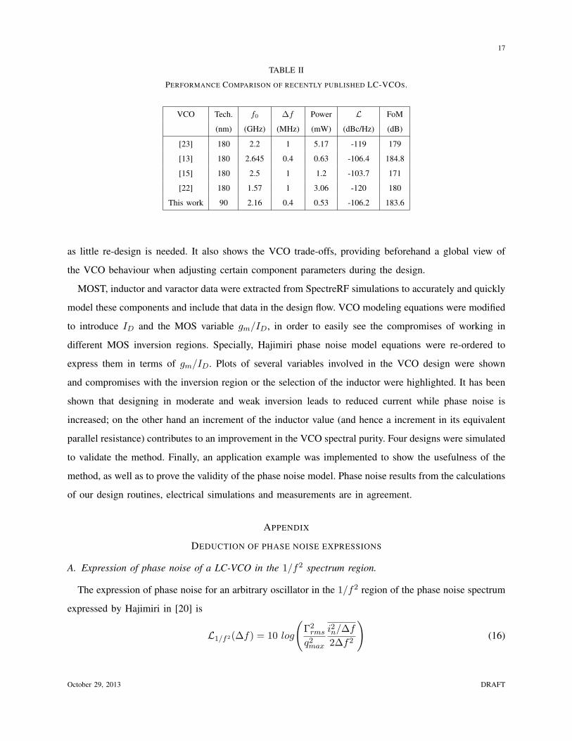
Table II compares the performance of the designed LC-VCO in moderate inversion with that of some
prior works, where the well known figure-of-merit (FoM) of the VCO defined in [22] is used. Our VCO
is well positioned considering other similar designs, as only the second one has a better FoM. However
the later occupies more area than our design because it uses two on-chip inductors, which increases the
tank quality factor and reduces the phase noise.
VIII. CONCLUSIONS
In this paper, an RF LC-VCO design methodology for nanometer technologies based on the gm/ID
technique has been presented. The methodology proposed enables a considerable design time reduction
October 29, 2013 DRAFT
17
TABLE II
PERFORMANCE COMPARISON OF RECENTLY PUBLISHED LC-VCOS.
VCO Tech. f0 ∆f Power L FoM
(nm) (GHz) (MHz) (mW) (dBc/Hz) (dB)
[23] 180 2.2 1 5.17 -119 179
[13] 180 2.645 0.4 0.63 -106.4 184.8
[15] 180 2.5 1 1.2 -103.7 171
[22] 180 1.57 1 3.06 -120 180
This work 90 2.16 0.4 0.53 -106.2 183.6
as little re-design is needed. It also shows the VCO trade-offs, providing beforehand a global view of
the VCO behaviour when adjusting certain component parameters during the design.
MOST, inductor and varactor data were extracted from SpectreRF simulations to accurately and quickly
model these components and include that data in the design flow. VCO modeling equations were modified
to introduce ID and the MOS variable gm/ID, in order to easily see the compromises of working in
different MOS inversion regions. Specially, Hajimiri phase noise model equations were re-ordered to
express them in terms of gm/ID. Plots of several variables involved in the VCO design were shown
and compromises with the inversion region or the selection of the inductor were highlighted. It has been
shown that designing in moderate and weak inversion leads to reduced current while phase noise is
increased; on the other hand an increment of the inductor value (and hence a increment in its equivalent
parallel resistance) contributes to an improvement in the VCO spectral purity. Four designs were simulated
to validate the method. Finally, an application example was implemented to show the usefulness of the
method, as well as to prove the validity of the phase noise model. Phase noise results from the calculations
of our design routines, electrical simulations and measurements are in agreement.
APPENDIX
DEDUCTION OF PHASE NOISE EXPRESSIONS
A. Expression of phase noise of a LC-VCO in the 1/f2 spectrum region.
The expression of phase noise for an arbitrary oscillator in the 1/f2 region of the phase noise spectrum
expressed by Hajimiri in [20] is
L1/f2(∆f) = 10 log
(Γ2rms
q2max
i2n/∆f2∆f2
)(16)
October 29, 2013 DRAFT

18
where Γrms is the rms value of the impulse sensitivity function ISF defined in [20], qmax is the maximum
charge displacement across the capacitor in the output nodes, ∆f is the frequency offset respect to the
oscillation frequency f0, and i2n/∆f is the power spectral density of the noise source considered at the
output nodes.
To evaluate the phase noise expression for our LC-VCO, let’s obtain the expressions of each term in
(16). Firstly we calculate the most important VCO white noise sources. For simplicity we will consider
that no correlation exists between them. Superposition will be applied when substituting their expressions
in (16).
The general expression of MOS white noise is [4]
i2w,MOS
∆f= 4kBTγgdo = 4kBT
γ
αgm. (17)
The equivalent power spectral density of the two nMOS and two pMOS is [24]
i2w,MOSeq
∆f=
12
(i2w,n∆f
+i2w,p∆f
) (18)
Substituting (17) in (18)
i2w,MOSeq
∆f∼= 4kBTγgm
12
( 1αn
+1αp
)= 4kBT
γ
αeq. (19)
The white noise of each cross-coupled transistor block due to its equivalent drain-source conductance
is [4] [25]:i2w,gds
∆f= 4kBT
gds2
= 4kBTgm2Ai
. (20)
Considering both nMOS and pMOS equivalent conductances,
i2w,geqds
∆f= 4kBT
gm2
( 1Ai,n
+1Ai,p
). (21)
The white noise of the inductor parallel resistance Rind = 1/gind is, applying (9),
i2w,Lind
∆f= 4kBTgind = 4kBT
gmk′osc
. (22)
The white noise power spectral density of the varactor has been neglected for this deduction as generally
gvar � gind.
October 29, 2013 DRAFT

19
The equivalent white noise power spectral density of the LC-VCO is, from equations, (8), (19), (21)
and (22):
i2w,V CO∆f
= 4kBTgm( γ
αeq+
1k′osc
+1
2Ai,n+
12Ai,p
)= 4kBTgm
( γ
αeq+
1kosc
)= 4kBTgmλ. (23)
Besides, qmax = CtankVout, where Ctank is the equivalent capacitance at the output nodes, expressed
as:
Ctank =1
4π2f20Lind
=Q
2πf0Rtank(24)
Then, from (10) and (24), qmax is
qmax =8π
IDQ
(2πf0)=
2IDRtank(π3)f2
0Lind. (25)
Finally, substituting (23) and (25) in (16), considering Γrms ≈ 0.5 due to the symmetry characteristics
of this VCO, and reordering the terms, we obtain
L1/f2(∆f) = 10 log
(kBT
π2
82λ
1Q2
gmID
1ID
f20
∆f2
)(26)
B. Expression of phase noise of a LC-VCO in the 1/f3 spectrum region.
From [20], the following is the general expression of the phase nose in the 1/f3 portion of the phase
noise spectrum
L(∆f)1/f3 = 10 log
(Γ2av
8q2max
i21/f/∆f∆f2
)(27)
Considering that only the MOS transistors injects flicker noise, the total power spectral density of the
flicker noise sources is
i21/f
∆f=
12
(i21/f,n
∆f+i21/f,p
∆f
)
=12
(K ′
F,ng2m
WnL+K
′
F,pg2m
WpL
) 1f
(28)
Equations (27) together with (25) and (28) results in the following expression for phase noise in the 1/f3
zone in terms of gm/ID:
L1/f3(∆f) = 10 log
(Γ2av
8π2
82
1L
(K
′
F,n
Wn+K
′
F,p
Wp
)
1Q2
(gmID
)2f2
0
∆f3
)(29)
October 29, 2013 DRAFT

20
C. Corner frequency of MOST expressed as a function of gm/ID and i.
The corner frequency of a MOST fc is obtained equaling the expressions of white noise and flicker
noise, resulting in:
fc =K
′
F
4kBTα
γ
gmID
IDW/L
1L2
=K
′
F
4kBTα
γ
gmIDi
1L2
(30)
D. Flicker corner frequency of the VCO phase noise expressed as a function of gm/ID and i.
The flicker corner frequency of the VCO phase noise, obtained when making equal the phase noise
expressions at white noise and flicker zones -(26) and (29), respectively-, results
fc,1/f3 = k0
( i2w,n fc,n + i2w,p fc,p
i2w,n + i2w,p
)= k0 fc,eq. (31)
where k0 =(
Γav
2Γrms
)2.
REFERENCES
[1] D. Leenaerts, J. van der Tang, and C. S. Vaucher, Circuit Design for RF Transceivers, 1st ed. Springer, 2001.
[2] F. Silveira, D. Flandre, and P. G. A. Jespers, “A gm/ID based methodology for the design of CMOS analog circuits and
its applications to the synthesis of a silicon-on-insulator micropower OTA,” IEEE Journal of Solid-State Circuits, vol. 31,
no. 9, pp. 1314–1319, Sep. 1996.
[3] P. G. Jespers, The gm/ID Methodology, a sizing tool for low-voltage analog CMOS Circuits. Springer, 2010.
[4] Y. Tsividis, Operation and Modelling of the MOS Transistor, 2nd ed. Oxford University Press, 2000.
[5] C. Enz and E. Vittoz, Charge-based MOS transistor modeling. John Wiley and Sons, 2006.
[6] A.Cunha, M. C. Schneider, and C. Galup-Montoro, “An MOS transistor model for analog circuit design,” IEEE Journal
of Solid-State Circuits, vol. 33, no. 10, pp. 1510–1519, Oct. 1998.
[7] C. Galup-Montoro, M. C. Schneider, and A. A. Cunha, “A current-based MOSFET model for integrated circuit design,”
in Low Voltage/Low Power Integrated Circuits and Systems, E. Snchez-Sinencio and A. Andreou, Eds. Piscataway, NJ:
IEEE Press, 1999, ch. 2, pp. 7–55.
[8] A.-S. Porret, T. Melly, D. Python, C. C. Enz, and E. A. Vittoz, “An ultralow -power UHF transceiver integrated in a standard
digital CMOS process: Architecture and receiver,” IEEE Journal of Solid-State Circuits, vol. 36, no. 3, pp. 452–464, Mar.
2001.
[9] T. Melly, A.-S. Porret, C. C. Enz, and E. A. Vittoz, “An ultralow -power UHF transceiver integrated in a standard digital
CMOS process: Transmitter,” IEEE Journal of Solid-State Circuits, vol. 36, no. 3, pp. 467–472, Mar. 2001.
[10] J. Ramos and et al, “90nm RF CMOS technology for low-power 900MHz applications,” Proceeding of the 34th European
Solid-State Device Research conference ESSDERC 2004, pp. 329–332, Sep. 2004.
[11] L. Barboni, R. Fiorelli, and F. Silveira, “A tool for design exploration and power optimization of CMOS RF circuit blocks,”
IEEE International Symposium on Circuits and Systems ISCAS’06, May 2006.
[12] R. Fiorelli, E. Peralıas, and F. Silveira, “Phase noise - consumption trade-off in low power RF-LC-VCO design in micro
and nanometric technologies,” in Proceedings of the 22th Symposium on Integrated Circuits and Systems Design (SBCCI).
Natal, Brazil: ACM, Set 2009.
October 29, 2013 DRAFT
21
[13] H. Lee and S. Mohammadi, “A subthreshold low phase noise CMOS LC VCO for ultra low power applications,” IEEE
Microwave and Wireless Component Letters, vol. 17, no. 11, pp. 796–799, Nov. 2007.
[14] H.-H. Hsieh and L.-H. Lu, “Design of ultra-low-voltage RF frontends with complementary current-reused architectures,”
IEEE Transactions on Microwave Theory and Techniques, vol. 55, no. 7, pp. 1445–1458, Jul. 2007.
[15] B. Perumana, S. Chakraborty, C.-H. Lee, and J. Laskar, “A low-power fully monolithic subthreshold CMOS receiver with
integrated LO generation for 2.4 GHz wireless PAN applications,” IEEE Journal of Solid-State Circuits, vol. 43, no. 10,
pp. 2229–2238, Oct 2008.
[16] G. Gildenblat, X. Li, W.Wu, H. Wang, A. Jha, R. van Langevelde, G. Smit, A. Scholten, and D. Klaassen, “PSP: An
advanced surface-potential-based MOSFET model for circuit simulation,” IEEE Transactions on Electron Devices, vol. 53,
no. 9, pp. 1979–1993, Sep. 2006.
[17] M. Manghisoni, L. Ratti, V. Re, V. Speziali, and G. Traversi, “Noise characterization of 130 nm and 90 nm CMOS
technologies for analog front-end electronics,” in 2006 IEEE Nuclear Science Symposium Conference Record., 2006, pp.
214–218.
[18] A. M. Niknejad, “Analysis of Si inductors and transformers for IC’s (ASITIC),” 2000, http://rfic.eecs.berkeley.edu/ nikne-
jad/asitic.html.
[19] A. Hajimiri and T. H. Lee, “Design issues in CMOS differential LC oscillators,” IEEE Journal of Solid-State Circuits,
vol. 34, no. 5, pp. 717–724, 1999.
[20] A. Hajimiri and T. Lee, “A general theory of phase noise in electrical oscillators,” IEEE Journal of Solid-State Circuits,
vol. 33, no. 2, pp. 179–194, Feb. 1998.
[21] D. Leeson, “A simple model of feedback oscillator noise spectrum,” Proceedings of the IEEE, vol. 54, pp. 329–330, Feb.
1966.
[22] K.-G. Park, C.-Y. Jeong, J.-W. Park, J.-W. Lee, J.-G. Jo, , and C. Yoo, “Current reusing VCO and divide-by-two frequency
divider for quadrature LO generation,” IEEE Microwave and Wireless Components Letters, vol. 18, no. 6, pp. 413–415,
Jun. 2008.
[23] L. L. K. Leung and H. C. Luong, “A 1 V 9.7 mW CMOS frequency synthesizer for IEEE 802.11a transceivers,” IEEE
Transactions on Microwave Theory and Techniques, vol. 56, no. 1, pp. 39–48, Jan. 2008.
[24] A. Hajimiri, Trade-offs in Analog Circuit Design. Kluwer Academic Publishers, 2002, ch. Trade offs in oscillator phase
noise, pp. 551–585.
[25] BSIM Research Group, “BSIM3v3 and BSIM4 MOS Model,” 2008, www-device.eecs.berkeley.edu/ bsim3/bsim4.html.
Rafaella Fiorelli Rafaella Fiorelli (S’05) was born in Montevideo, Uruguay in 1978. She received her
B.Sc. and M.Sc. degrees in Electrical Engineering from the Universidad de la Republica, Montevideo,
Uruguay, in 2002 and 2005 respectively. She is currently working towards the doctoral degree in electrical
engineering. In 2003 she joined the Electrical Engineering Institute of the Universidad de la Republica,
Uruguay. From 2009 she is working in the IMSE-CNM of Seville, Spain, with a MAE-AECIC Spanish
government grant. Her current research includes the implementation of design methodologies of low power
RF blocks and BIST test in RF.
October 29, 2013 DRAFT
22
Eduardo Peralas Eduardo J. Peralıas received the Ph.D. degree from the University of Seville, (Spain)
in 1999. Since 2001, he has been with the Instituto de Microelectronica de Sevilla (IMSE-CNM-CSIC),
where he is currently a Tenured Scientist. His main research interests have been in the areas of Mixed
Design with emphasis on Analog-to-Digital converters, Test and Design for Testability of Analog and
Mixed-Signal Circuits, and Statistical Behavioral Modeling.
Fernando Silveira Fernando Silveira (S’89- M’90- SM’03) received the Electrical Engineering degree
from Universidad de la Republica, Uruguay in 1990 and the MSc. and PhD degree in Microelectronics
from Universite catholique de Louvain, Belgium in, respectively, 1995 and 2002. He is currently Professor
at the Electrical Engineering Department of the School of Engineering of Universidad de la Republica,
Uruguay. His research interests are in design of ultra low-power analog and RF integrated circuits and
systems, in particular with biomedical application. In this field, he is co-author of one book and many
technical articles. He has had multiple industrial activities with CCC Medical Devices and NanoWattICs, including leading
the design of an ASIC for implantable pacemakers and designing analog circuit modules for implantable devices for various
companies worldwide.
October 29, 2013 DRAFT

23
Fig. 10. L1/f2 in dBc/Hz mapped versus gm/ID and Lind. The text-box displays the characteristics and parameters of the
LC-VCO associated with the picked point (P4 in this example).
Fig. 11. Phase noise SpectreRF simulations for designs P1, P2, P3 and P4.
October 29, 2013 DRAFT

24
Fig. 12. Layout and microphotograph of the fabricated VCO.
Fig. 13. Carrier frequency f0 versus Vcontrol and output spectrum (inset) at Vcontrol = 0 with the buffer switched off.
October 29, 2013 DRAFT

25
Fig. 14. L with the VCO biased with Ibias = 2 · ID = 440µA and f0 = 2.1639GHz (buffer switched off). 1/f2 and 1/f3
slopes are shown as well as the estimated flicker corner fc,1/f3 .
Fig. 15. Phase noise measured and estimated by (11) sweeping only ID .
October 29, 2013 DRAFT