Bahram Sanadgol - Kontaktangabenhft.uni-duisburg-essen.de/arbeiten/Vortrag_Sanadgol_Bahram.pdf ·...
30
11.06.2007 Bahram Sanadgol 1 Master Thesis Control and Prediction of Scan Blindness Effects in Printed Planar Antenna Systems Bahram Sanadgol Universität Duisburg-Essen: Prof. Dr.-Ing. K. Solbach Dipl.-Ing. Oliver Litschke, IMST GmbH
-
Upload
duongtuong -
Category
Documents
-
view
225 -
download
1
Transcript of Bahram Sanadgol - Kontaktangabenhft.uni-duisburg-essen.de/arbeiten/Vortrag_Sanadgol_Bahram.pdf ·...
11.06.2007 Bahram Sanadgol 1
Master Thesis
Control and Prediction of Scan Blindness Effects in Printed Planar Antenna Systems
Bahram Sanadgol
Universität Duisburg-Essen: Prof. Dr.-Ing. K. Solbach
Dipl.-Ing. Oliver Litschke, IMST GmbH
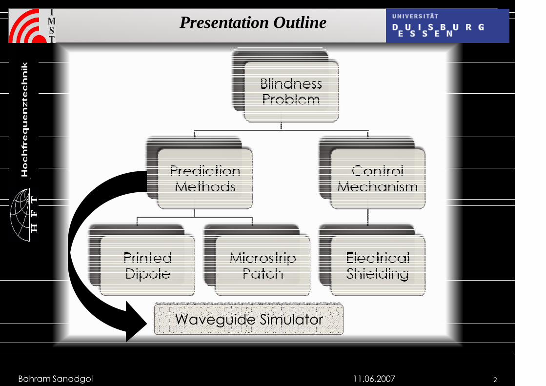
Presentation Outline
11.06.2007 Bahram Sanadgol 2
Waveguide Simulator

Blindness Concept
11.06.2007 Bahram Sanadgol 3
TM TE
•Null in Pattern •Scan Coverage •Big Mismatch in Input Impedance •No Feeding Possible
E E
Substrate u=sin θ cos Ф

Surface Wave Circle Diagram
11.06.2007 Bahram Sanadgol 4
Scanning Part
Blind
Spot
Blindness in Visible Space
TM (TE) mode excitation
X→0.55λ
y→ 0.5 λ and β=1.3

Scan Impedance Method and SEP
11.06.2007 Bahram Sanadgol 5

Effective Propagation Constant
11.06.2007 Bahram Sanadgol 6

TM Mode β Calculation
11.06.2007 Bahram Sanadgol 7
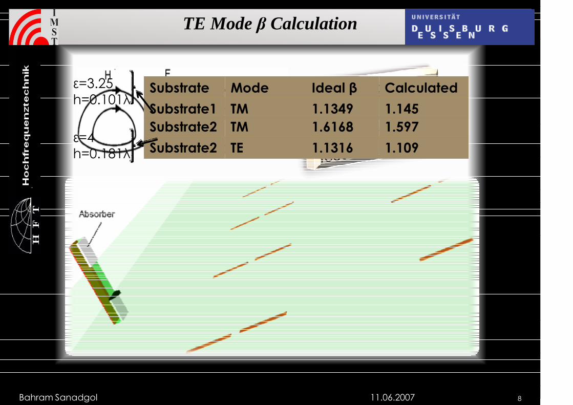
TE Mode β Calculation
11.06.2007 Bahram Sanadgol 8
Substrate Mode Ideal β Calculated
β Substrate1 TM 1.1349 1.145
Substrate2
2
TM 1.6168 1.597
Substrate2 TE 1.1316 1.109
ε=3.25
h=0.101λ
ε=4
h=0.181λ

Substrate Mode β
effective
β
Theory
Substrate1 TM 1.124 1.1349
Substrate2 TM 1.4 1.6168
Substrate2
TE 1.177 1.1316
Printed Dipole
11.06.2007 Bahram Sanadgol 9

Method Comparison for Dipole
11.06.2007 Bahram Sanadgol 10
Spacing Spacing
Surface Wave
SEP Scan
Impedance
β effective
Surface Wave
SEP Scan
Impedance
β effective
(1.1349)
(1.6168)
Spacing Substrate Surface Wave SEP Scan Impedance β Effective

Patch Array
11.06.2007 Bahram Sanadgol 11

Arrays of Microstrip Patches
11.06.2007 Bahram Sanadgol 12
Scan Element Pattern
ε=3.48
h=0.121λ β=1.2383

Scan Resistance, E-plane
11.06.2007 Bahram Sanadgol 13

Scan Reactance, E-plane
11.06.2007 Bahram Sanadgol 14

Scan Resistance, H-plane
11.06.2007 Bahram Sanadgol 15

Scan Reactance, H-plane
11.06.2007 Bahram Sanadgol 16

E-plane Farfield and Comparison
11.06.2007 Bahram Sanadgol 17
Spacing Surface Wave SEP Scan Impedance β effective
Element Spacing= 0.55 λ

Blindness Control
11.06.2007 Bahram Sanadgol 18

Wall’s Functionality
11.06.2007 Bahram Sanadgol 19
18 GHz 24 GHz

Effect of Wall on Resonant Frequency
11.06.2007 Bahram Sanadgol 20
Near Field Interference
Frequency Up-shift
Match Improvement from Suppressed Surface Wave
Single Element Tuning
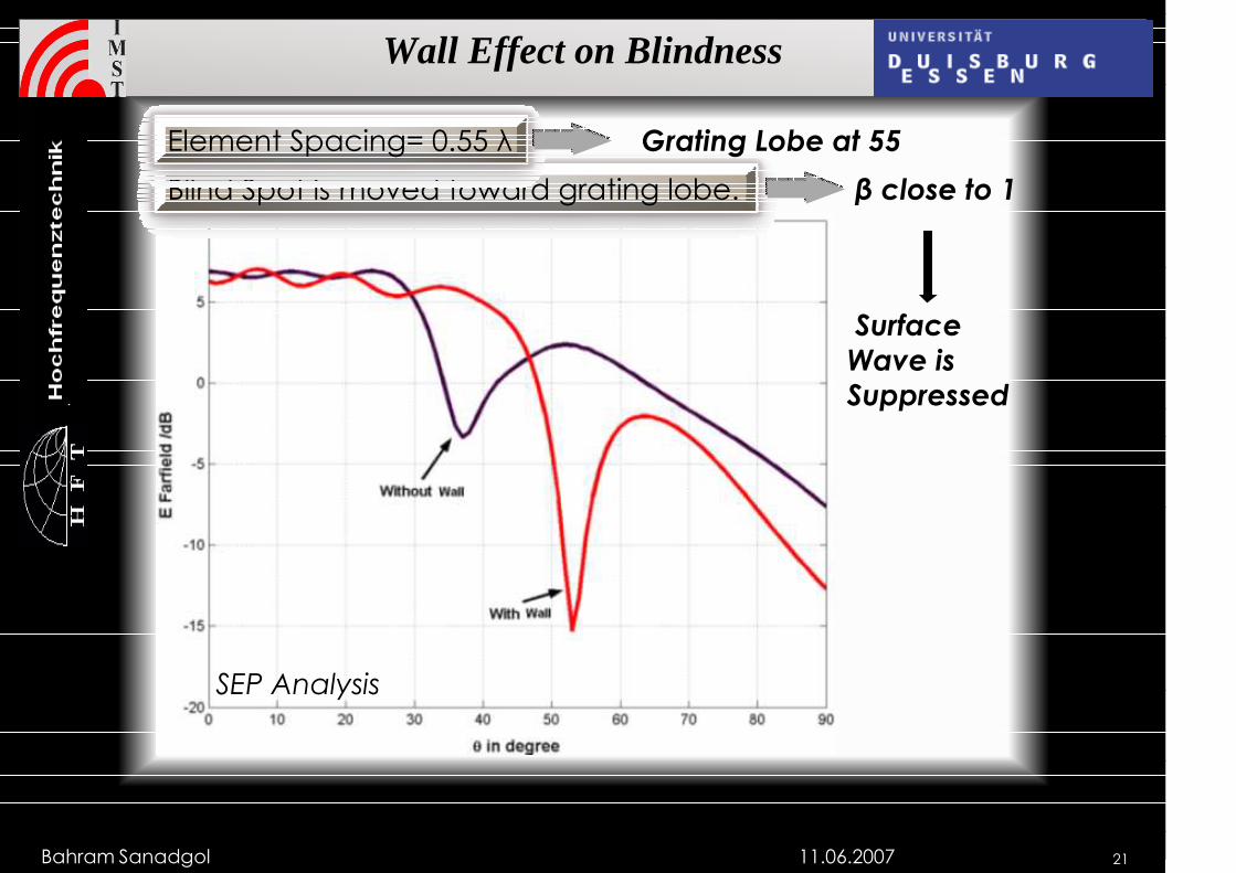
Wall Effect on Blindness
11.06.2007 Bahram Sanadgol 21
Blind Spot is moved toward grating lobe.
Element Spacing= 0.55 λ
Surface
Wave is
Suppressed
SEP Analysis
Grating Lobe at 55
β close to 1

Farfield Comparison
11.06.2007 Bahram Sanadgol 22
50
Element Spacing= 0.55 λ

Waveguide Simulator
11.06.2007 Bahram Sanadgol 23
Wav
egu
ide
Po
rt
Ele
men
t P
ort
Dipole Array, Spacing o.5λ
3*3 on a substrate with h=0.181λ
28°
24 GHz
E-plane

Farfield
11.06.2007 Bahram Sanadgol 24
Farfield pattern of a 1inear array of 17 dipoles on a
substrate with ε=4.2 from Scan Impedance Method

Conclusion and Future Work
11.06.2007 Bahram Sanadgol 25
•Blindness prediction for dipoles and patches
•New method based on β calculations
•Blindness control
•Waveguide simulation as comparison
•β calculations for other single elements
•Optimized feeding network
•Another suppressing structures

11.06.2007 Bahram Sanadgol 26

11.06.2007 Bahram Sanadgol 27

Patch Serial Feeding
11.06.2007 Bahram Sanadgol 28
Why? Simple Feeding Network
Easy to introduce phase shifters
Disadvantages
Pin’s Spurious Radiation
Amplitude Distribution

Amplitude Distribution and Layout
11.06.2007 Bahram Sanadgol 29
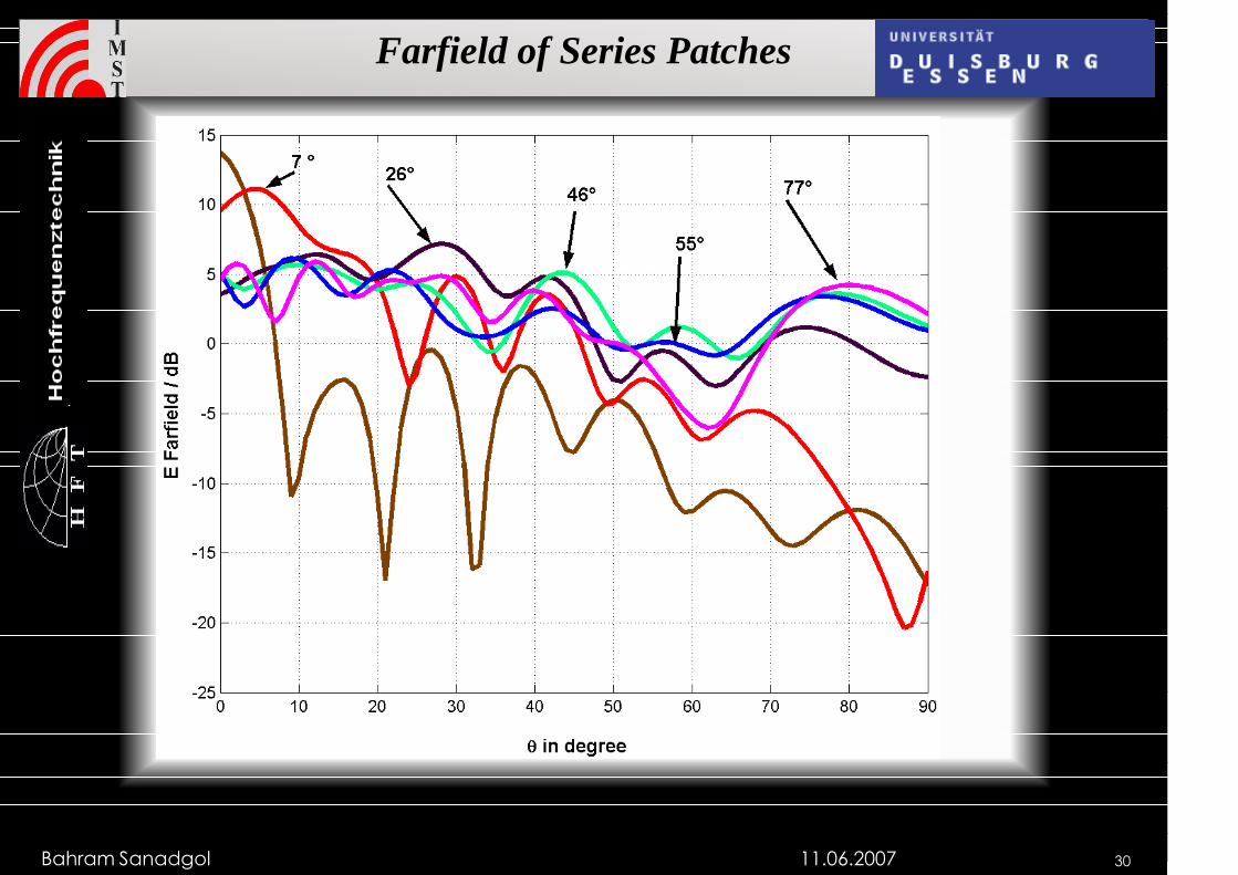
Farfield of Series Patches
11.06.2007 Bahram Sanadgol 30


![[Bahram Farahmand] Fracture Mechanics of Metals, C(BookFi.org)](https://static.fdocuments.us/doc/165x107/55cf9a81550346d033a21084/bahram-farahmand-fracture-mechanics-of-metals-cbookfiorg.jpg)