Background Statement for SEMI Draft Document 5744A Line Item...
22
Background Statement for SEMI Draft Document 5744A Line Item Revision to M49-1014, GUIDE FOR SPECIFYING GEOMETRY MEASUREMENT SYSTEMS FOR SILICON WAFERS FOR THE 130 nm TO 16 nm TECHNOLOGY GENERATIONS Notice: This background statement is not part of the balloted item. It is provided solely to assist the recipient in reaching an informed decision based on the rationale of the activity that preceded the creation of this Document. Notice: Recipients of this Document are invited to submit, with their comments, notification of any relevant patented technology or copyrighted items of which they are aware and to provide supporting documentation. In this context, “patented technology” is defined as technology for which a patent has issued or has been applied for. In the latter case, only publicly available information on the contents of the patent application is to be provided. Notice: Additions are indicated by underline and deletions are indicated by strikethrough. Background Along with advanced technology, wafer geometry values are being more critical. Recent edge exclusion reduction discussion may impact wafer geometry evaluation with laser marks, fiducial notch and/or wafer handling contacts whose measurement data is not acquired and/or is not used in the calculation of metrics. Therefore M49, Guide for specifying geometry measurement system, need to clarify this area of exclusion windows. Unfortunately current description of these area are not clear and to be revise version. LINE ITEM 1: Add 4.1.1 and Note 1. Add more specific description for exclusion windows at section 5.5.22, rewrite section 3.4 at table 3 and table 4, and maintain update in the table 2. Per SEMI Procedure Manual 3.4.3.3.1, a Line-item Ballot should include the purpose, scope, limitations (if present), and terminology (if present) sections, along with the full text of any section to which revisions are being balloted. Voter requests for access to the full Standard or Safety Guideline must be made at least three business days before the voting deadline. Late requests may not be honored. Review Information Task Force Review Committee Review Group: International Advanced Wafer Geometry TF Silicon Wafer NA TC Chapter Committee Date: Monday, July 11, 2016 Tuesday, July 12, 2016 Time & Time zone: 14:00-17:00 13:00-16:00 Location: San Francisco Marriott San Francisco Marriott City, State/Country: San Francisco, CA, USA San Francisco, CA, USA Leader(s): Jaydeep Sinha ( [email protected]) N Poduje SMS ([email protected]) N Poduje SMS ([email protected]) Denish Guputa ([email protected]) Standards Staff: [email protected] [email protected] This meeting’s details are subject to change, and additional review sessions may be scheduled if necessary. Contact the task force leaders or Standards staff for confirmation. If you would like to attend these meetings in person but would like to participate by telephone/web, please contact Standards staff. Check www.semi.org/standards on calendar of event for the latest meeting schedule.
Transcript of Background Statement for SEMI Draft Document 5744A Line Item...
Background Statement for SEMI Draft Document 5744A
Line Item Revision to M49-1014, GUIDE FOR SPECIFYING GEOMETRY MEASUREMENT SYSTEMS FOR SILICON WAFERS FOR THE 130 nm TO 16 nm TECHNOLOGY GENERATIONS Notice: This background statement is not part of the balloted item. It is provided solely to assist the recipient in reaching an informed decision based on the rationale of the activity that preceded the creation of this Document.
Notice: Recipients of this Document are invited to submit, with their comments, notification of any relevant patented technology or copyrighted items of which they are aware and to provide supporting documentation. In this context, “patented technology” is defined as technology for which a patent has issued or has been applied for. In the latter case, only publicly available information on the contents of the patent application is to be provided.
Notice: Additions are indicated by underline and deletions are indicated by strikethrough.
Background Along with advanced technology, wafer geometry values are being more critical. Recent edge exclusion reduction discussion may impact wafer geometry evaluation with laser marks, fiducial notch and/or wafer handling contacts whose measurement data is not acquired and/or is not used in the calculation of metrics. Therefore M49, Guide for specifying geometry measurement system, need to clarify this area of exclusion windows. Unfortunately current description of these area are not clear and to be revise version.
LINE ITEM 1: Add 4.1.1 and Note 1. Add more specific description for exclusion windows at section 5.5.22, rewrite section 3.4 at table 3 and table 4, and maintain update in the table 2.
Per SEMI Procedure Manual 3.4.3.3.1, a Line-item Ballot should include the purpose, scope, limitations (if present), and terminology (if present) sections, along with the full text of any section to which revisions are being balloted. Voter requests for access to the full Standard or Safety Guideline must be made at least three business days before the voting deadline. Late requests may not be honored.
Review Information
Task Force Review Committee Review
Group: International Advanced Wafer Geometry TF Silicon Wafer NA TC Chapter Committee
Date: Monday, July 11, 2016 Tuesday, July 12, 2016
Time & Time zone: 14:00-17:00 13:00-16:00
Location: San Francisco Marriott San Francisco Marriott
City, State/Country: San Francisco, CA, USA San Francisco, CA, USA
Leader(s): Jaydeep Sinha ( [email protected]) N Poduje SMS ([email protected])
N Poduje SMS ([email protected]) Denish Guputa ([email protected])
Standards Staff: [email protected] [email protected]
This meeting’s details are subject to change, and additional review sessions may be scheduled if necessary. Contact the task force leaders or Standards staff for confirmation.
If you would like to attend these meetings in person but would like to participate by telephone/web, please contact Standards staff.
Check www.semi.org/standards on calendar of event for the latest meeting schedule.
This is a Draft Document of the SEMI International Standards program. No material on this page is to be construed as an official or adopted Standard or Safety Guideline. Permission is granted to reproduce and/or distribute this document, in whole or in part, only within the scope of SEMI International Standards committee (document development) activity. All other reproduction and/or distribution without the prior written consent of SEMI is prohibited.
Page 1 Doc. 5744A SEMI
Semiconductor Equipment and Materials International 3081 Zanker Road San Jose, CA 95134-2127 Phone: 408.943.6900, Fax: 408.943.7943
LE
TT
ER
BA
LL
OT
DRAFTDocument Number: 5744A
Date: 3/11/2016
SEMI Draft Document 5744A
Line Item Revision to M49-1014, GUIDE FOR SPECIFYING GEOMETRY MEASUREMENT SYSTEMS FOR SILICON WAFERS FOR THE 130 nm TO 16 nm TECHNOLOGY GENERATIONS Notice: Additions are indicated by underline and deletions are indicated by strikethrough.
LINE ITEM 1: Add 4.1.1 and Note 1. Add more specific description for exclusion windows at section 5.5.22, rewrite section 3.4 at table 3 and table 4, and maintain update in the table 2.
1 Purpose
1.1 This Guide provides recommendations for specifying measurement systems for geometry and flatness of silicon wafers of the 130, 90, 65, 45, 32, 22, and 16 nm technology generation as anticipated by the International Technology Roadmap for Semiconductors (ITRS) and in the forecasts of the major manufacturers of semiconductor devices. Wafer parameters as defined by SEMI M1, SEMI M8, SEMI M11, SEMI M24, or SEMI M38 are specified by customers of silicon wafer suppliers and are usually part of Certificates of Compliance. Suppliers of silicon wafers and their customers might measure these parameters using equipment provided by different manufacturers of such equipment or using different generations of equipment of one supplier. Agreement on basic features and capability of such measurement systems improves data exchange and interpretation of data as well as procurement of appropriate measurement systems.
2 Scope
2.1 This Guide outlines and recommends basic specifications for systems for measuring geometry and flatness of silicon wafers of the 130, 90, 65, 45, 32, 22, and 16 nm technology generation.
2.2 This Guide applies to measurement systems used for verifying the quality parameters geometry and flatness in large scale production of bare polished or epitaxial silicon wafers the backside of which may be acid etched and/or covered by unpatterned, homogeneous layers of, for example, poly-Si or low temperature oxide (LTO). Artifacts (e.g., reference materials) for calibrating a measurement system might have different properties.
2.3 This Guide also applies to measurement systems that provide only a subset of the measurement features outlined in this Guide.
2.4 The Guide does not apply to measurement systems used to control intermediate process steps during Si wafer manufacturing. However, it may be completely or partly used for measurement systems for those applications provided corresponding constraints are appropriately identified.
2.5 The Guide also does not apply to measurement systems for SOI wafers or patterned wafers.
NOTICE: SEMI Standards and Safety Guidelines do not purport to address all safety issues associated with their use. It is the responsibility of the users of the Documents to establish appropriate safety and health practices, and determine the applicability of regulatory or other limitations prior to use.
3 Referenced Standards and Documents
3.1 SEMI Standards and Safety Guidelines
SEMI E1.9 — Mechanical Specification for Cassettes Used to Transport and Store 300 mm Wafers
SEMI E5 — SEMI Equipment Communications Standard 2 Message Content (SECS-II)
SEMI E10 — Specification for Definition and Measurement of Equipment Reliability, Availability, and Maintainability (RAM) and Utilization
SEMI E19 — Standard Mechanical Interface (SMIF)
SEMI E30 — Generic Model for Communications and Control of Manufacturing Equipment (GEM)

This is a Draft Document of the SEMI International Standards program. No material on this page is to be construed as an official or adopted Standard or Safety Guideline. Permission is granted to reproduce and/or distribute this document, in whole or in part, only within the scope of SEMI International Standards committee (document development) activity. All other reproduction and/or distribution without the prior written consent of SEMI is prohibited.
Page 2 Doc. 5744A SEMI
Semiconductor Equipment and Materials International 3081 Zanker Road San Jose, CA 95134-2127 Phone: 408.943.6900, Fax: 408.943.7943
LE
TT
ER
BA
LL
OT
DRAFTDocument Number: 5744A
Date: 3/11/2016
SEMI E37 — High Speed SECS Message Services (HSMS) Generic Services
SEMI E47 — Specification for 150 mm/200 mm Pod Handles
SEMI E47.1 — Mechanical Specification for FOUPS Used to Transport and Store 300 mm Wafers
SEMI E58 — Automated Reliability, Availability, and Maintainability Standard (ARAMS): Concepts, Behavior, and Services
SEMI E89 — Guide for Measurement System Analysis (MSA)
SEMI E158 — Mechanical Specification for Fab Wafer Carrier Used to Transport and Store 450 mm Wafers (450 FOUP) and Kinematic Coupling
SEMI E159 — Mechanical Specification for Multi Application Carrier (MAC) Used to Transport and Ship 450 mm Wafers
SEMI M1 — Specifications for Polished Single Crystal Silicon Wafers
SEMI M8 — Specification for Polished Monocrystalline Silicon Test Wafers
SEMI M12 — Specification for Serial Alphanumeric Marking of the Front Surface of Wafers
SEMI M13 — Specification for Alphanumeric Marking of Silicon Wafers
SEMI M24 — Specification for Polished Monocrystalline Silicon Premium Wafers
SEMI M31 — Mechanical Specification for Front-Opening Shipping Box Used to Transport and Ship 300 mm Wafers
SEMI M38 — Specification for Polished Reclaimed Silicon Wafers
SEMI M43 — Guide for Reporting Wafer Nanotopography
SEMI M59 — Terminology for Silicon Technology
SEMI M62 — Specifications for Silicon Epitaxial Wafers
SEMI M67 — Practice for Determining Wafer Near-Edge Geometry from a Measured Thickness Data Array Using the ESFQR, ESFQD and ESBIR Metrics
SEMI M68 — Practice for Determining Wafer Near-Edge Geometry from a Measured Height Data Array Using a Curvature Metric, ZDD
SEMI M73 — Test Methods for Extracting Relevant Characteristics from Measured Wafer Edge Profiles
SEMI M80 — Mechanical Specification for Front-Opening Shipping Box Used to Transport and Ship 450 mm Wafers
SEMI MF42 — Test Methods for Conductivity Type of Extrinsic Semiconducting Materials
SEMI MF84 — Test Method for Measuring Resistivity of Silicon Wafers with an In-Line Four-Point Probe
SEMI MF534 — Test Method for Bow of Silicon Wafers
SEMI MF657 — Test Method for Measuring Warp and Total Thickness Variation on Silicon Wafers by Noncontact Scanning
SEMI MF671 — Test Method for Measuring Flat Length on Wafers of Silicon and Other Electronic Materials
SEMI MF673 — Test Methods for Measuring Resistivity of Semiconductor Wafers or Sheet Resistance of Semiconductor Films with a Noncontact Eddy-Current Gauge
SEMI MF928 — Test Methods for Edge Contour of Circular Semiconductor Wafers and Rigid Disk Substrates
SEMI MF1152 — Test Method for Dimensions of Notches on Silicon Wafers
SEMI MF1390 — Test Method for Measuring Bow and Warp on Silicon Wafers by Automated Noncontact Scanning
This is a Draft Document of the SEMI International Standards program. No material on this page is to be construed as an official or adopted Standard or Safety Guideline. Permission is granted to reproduce and/or distribute this document, in whole or in part, only within the scope of SEMI International Standards committee (document development) activity. All other reproduction and/or distribution without the prior written consent of SEMI is prohibited.
Page 3 Doc. 5744A SEMI
Semiconductor Equipment and Materials International 3081 Zanker Road San Jose, CA 95134-2127 Phone: 408.943.6900, Fax: 408.943.7943
LE
TT
ER
BA
LL
OT
DRAFTDocument Number: 5744A
Date: 3/11/2016
SEMI MF1451 — Test Method for Measuring Sori on Silicon Wafers by Automated Noncontact Scanning
SEMI MF1530 — Test Method for Measuring Flatness, Thickness, and Thickness Variation on Silicon Wafers by Automated Noncontact Scanning
SEMI MF2074 — Guide for Measuring Diameter of Silicon and Other Semiconductor Wafers
SEMI T7 — Specification for Back Surface Marking of Double-Side Polished Wafers with a Two-Dimensional Matrix Code Symbol
3.2 DIN Standards1
DIN 50431 — Measurement of the Electrical Resistivity of Silicon or Germanium Single Crystals by Means of the Four-Point-Probe Direct Current Method with Collinear Probe Array
DIN 50432 — Determination of the Conductivity Type of Silicon or Germanium by Means of Rectification Test or Hot-Probe
DIN 50441-1 — Determination of the Geometric Dimensions of Semiconductor Slices; Measurement of Thickness
DIN 50441-2 — Determination of the Geometric Dimensions of Semiconductor Slices; Testing of Edge Rounding
DIN 50441-4 — Determination of the Geometric Dimensions of Semiconductor Slices; Diameter and Flat Depth of Slices
DIN 50441-5 — Determination of the Geometric Dimensions of Semiconductor Wafers; Terms of Shape and Flatness Deviation
DIN 50445 — Contactless Determination of the Electrical Resistivity of Semiconductor Wafers with the Eddy Current Method
3.3 IEEE Standards2
IEEE 754 — IEEE Standard for Binary Floating-Point Arithmetic
IEEE 802 — IEEE Standard for Local and Metropolitan Networks: Overview and Architecture
IEEE 854 — IEEE Standard Radix-Independent Floating-Point Arithmetic
3.4 ISO Standards3
ISO/IEC 8859 — Information Technology – 8-bit Single-Byte Coded Graphic Character Sets
ISO 8879 — Information Processing – Text and Office Systems – Standard Generalized Markup Language (SGML)
ISO 9000 — Quality Management Systems – Fundamentals and Vocabulary
ISO 9001 — Quality Management Systems – Requirements
ISO/IEC 10646-1 — Information Technology – Universal Multiple-Octet Character Set (UCS) – Part 1: Architecture and Basic Multilingual Plane
ISO/IEC 10918 — Information Technology – Digital Compression and Coding of Continuous-Tone Still Images
ISO 14644-1 — Cleanroom and Associated Controlled Environments – Part 1: Classification of Air Cleanliness
3.5 JEITA Standard4
JEITA EM-3401 (43) — Terminology of Silicon Wafer Flatness
1 Deutsches Institut für Normung e.V., Available from Beuth Verlag GmbH, Burggrafenstrasse 4-10, D-10787 Berlin, Germany; http://www.din.de 2 Institute of Electrical and Electronics Engineers, 3 Park Avenue, 17th Floor, New York, NY 10016-5997, USA; Telephone: 212.419.7900, Fax: 212.752.4929, http://www.ieee.org 3 International Organization for Standardization, ISO Central Secretariat, 1, ch. de la Voie-Creuse, CP 56, CH-1211 Geneva 20, Switzerland; Telephone: 41.22.749.01.11, Fax: 41.22.733.34.30, http://www.iso.org 4 Japan Electronics and Information Technology Industries Association, Ote Center Building, 1-1-3, Otemachi, Chiyoda-ku, Tokyo 100-0004, Japan; http://www.jeita.or.jp

This is a Draft Document of the SEMI International Standards program. No material on this page is to be construed as an official or adopted Standard or Safety Guideline. Permission is granted to reproduce and/or distribute this document, in whole or in part, only within the scope of SEMI International Standards committee (document development) activity. All other reproduction and/or distribution without the prior written consent of SEMI is prohibited.
Page 4 Doc. 5744A SEMI
Semiconductor Equipment and Materials International 3081 Zanker Road San Jose, CA 95134-2127 Phone: 408.943.6900, Fax: 408.943.7943
LE
TT
ER
BA
LL
OT
DRAFTDocument Number: 5744A
Date: 3/11/2016
NOTICE: Unless otherwise indicated, all documents cited shall be the latest published versions.
4 Terminology
4.1 General terms, acronyms, abbreviations and symbols associated with silicon technology and used in this Standard are listed and defined in SEMI M59.
4.1.1 exclusion window — an area on the wafer front or back surface that intersects the FQA from which acquired data, if any, are not used to calculate metrics.
NOTE 1 : Exclusion windows may be used when: a) wafer suppliers and buyers agree to exempt certain areas in the vicinity of mandated features, such as notches and laser scribes, that affect metrics; b) a given measurement system’s design precludes valid data acquisition, such as portions of the edge obscured by mechanical fixtures in the vicinity
5 Recommended Specification for Geometry Measurement Systems for Silicon Wafers
5.1 The recommended specifications are structured in three sections (Tables 1 through 5):
Generic Equipment Characteristics (Table 1)
Materials to be measured (Table 2)
Metrology Specific Equipment Characteristics (Tables 3, 4, and 5)
5.2 Tables 1 through 5 contain the specifications, referenced documents, test methods, and comments. Additional explanations and discussions are provided in this section.
5.3 Generic Equipment Characteristics (Table 1)
5.3.1 The section ‘Generic Equipment Characteristics’ consists of five subsections:
Wafer handling
Reliability
Procedural
Documentation
Computer/User Interface/Connectivity
5.3.2 Subsections covering ‘Facilities Requirements’ and ‘Safety/Legal/Regulatory’ are not included in the present document as these issues are highly user specific and dependent on national regulations.
5.4 Materials to be Measured (Table 2)
5.4.1 Table 2 specifies the parameters of silicon wafers that the measurement system must be capable to handle and to measure.
5.5 Metrology Specific Equipment Characteristics (Tables 3, 4, and 5)
5.5.1 This section specifies the dimensional parameters of silicon wafers to be measured and to be reported by systems for measuring the geometry and flatness of wafers as well as the required spatial resolution, precision and accuracy of the measurement system.
5.5.2 The ability of a measurement system to properly measure surface features of different spatial wavelengths is affected by the spatial bandwidth of the measurement system’s response function. Spatial bandwidth can be defined in many ways and is influenced by many factors beyond the scope of this Document. Some of these need to be standardized.
NOTE 1: Some of these factors may need to be standardized. Additional information related to this topic can be found in: Mathematical Principles of Signal Processing, Pierre Brémaud, Springer, New York, 2002.
This is a Draft Document of the SEMI International Standards program. No material on this page is to be construed as an official or adopted Standard or Safety Guideline. Permission is granted to reproduce and/or distribute this document, in whole or in part, only within the scope of SEMI International Standards committee (document development) activity. All other reproduction and/or distribution without the prior written consent of SEMI is prohibited.
Page 5 Doc. 5744A SEMI
Semiconductor Equipment and Materials International 3081 Zanker Road San Jose, CA 95134-2127 Phone: 408.943.6900, Fax: 408.943.7943
LE
TT
ER
BA
LL
OT
DRAFTDocument Number: 5744A
Date: 3/11/2016
5.5.3 Spatial resolution is defined by the high spatial frequency limit of the bandwidth of the measurement system’s response function.
5.5.4 Low and high cut-off frequency fmin and fmax define the bandwidth of the response function of measurement systems. The cut-off frequencies correspond to an attenuation of 0.5 for the amplitude of a sinusoidal surface feature with the exception of a low pass filter (fmin = 0) for which the attenuation remains 1 at fmin.
5.5.5 The rate of change of the attenuation approaching the cut-off frequencies has to be larger than the rate of a Gaussian filter with the corresponding cut-off frequency.
5.5.6 This Guide recommends values of fmax and fmin that the measurement system must be capable of measuring.
5.5.7 Any variations in filtering procedures applied near the FQA boundary must be described by the supplier of the measurement system.
5.5.8 The bandwidth as specified in Tables 3 and 4 is a nominal value.
5.5.9 This Guide uses a hierarchy of variability levels to describe the performance of a measurement system that is calibrated and adjusted/aligned according to the supplier’s procedures. The various terms are defined in SEMI M59.
5.5.9.1 Level 1 variability: standard deviation σ1
5.5.9.2 Level 2 variability: standard deviation σ2
5.5.9.3 Level 3 variability: standard deviation σ3
5.5.10 In addition two levels of systematic off-set between different measurement systems are defined:
5.5.10.1 Matching tolerance (difference of means Δm)
5.5.10.2 Correlation (regression curve)
5.5.11 Explicitly specified in the present document are only level 3 variability σ3 and matching tolerance Δm as they correspond to the utilization of measurement systems for wafer manufacturing most closely. The supplier of a specific measurement system may optionally provide specifications for level 1 and/or level 2 variability, respectively.
NOTE 2: In the absence of certified or standard reference materials matching may be tested by using appropriate wafers complying with 130, 90, 65, 45, 32, 22, or 16 nm technology node specifications, as appropriate. It is recommended to test for matching with a set of samples covering the parameter range of interest.
5.5.12 Level 3 variability σ3 and matching tolerance Δm are specified with respect to anticipated specifications for wafer geometry and flatness as given in Tables 3 and 4 for a reference wafer.
5.5.13 In the present document P/T-ratios (precision-to-tolerance ratios, see SEMI E89) are used for specifying level 3 variability σ3.
NOTE 3: P/T-ratio is a metric for assessing the capability of metrology equipment for verifying a specimen (e.g., Si wafer) specification.
5.5.13.1 A P/T-ratio of 30% or less is recommended in SEMI E89 for metrology equipment. Geometry characteristics of Si wafers typically display either an approximately symmetric distribution around a median (a two-sided distribution), or a strongly skewed distribution with the median approaching zero, the lower specification boundary (a one-sided distribution). Therefore the P/T ratio is calculated either based on a 3 σ criterion for one-sided distributions or a 6 σ criterion for two-sided distributions and two grades are recommended for flatness and geometry measurement systems (see also R1):
Grade A: P/T < 10%, 3 σ3 (one-sided distribution) or P/T < 10%, 6 3 (two-sided distribution)
Grade B: P/T < 20%, 3 σ3 (one-sided distribution) or P/T < 20%, 6 3 (two-sided distribution)
5.5.13.2 The individual measurement features a measurement system provides may be graded differently (e.g., SFQR might meet grade A, but SBIR only grade B). This has to be indicated appropriately in the measurement systems’ technical specifications.

This is a Draft Document of the SEMI International Standards program. No material on this page is to be construed as an official or adopted Standard or Safety Guideline. Permission is granted to reproduce and/or distribute this document, in whole or in part, only within the scope of SEMI International Standards committee (document development) activity. All other reproduction and/or distribution without the prior written consent of SEMI is prohibited.
Page 6 Doc. 5744A SEMI
Semiconductor Equipment and Materials International 3081 Zanker Road San Jose, CA 95134-2127 Phone: 408.943.6900, Fax: 408.943.7943
LE
TT
ER
BA
LL
OT
DRAFTDocument Number: 5744A
Date: 3/11/2016
5.5.14 Matching tolerance is specified to be less or equal to 1.5 times level 3 variability (1.5 3). This corresponds to a greater than 99% probability that the difference of any individual measurement results obtained with two different measurement systems is smaller or equal to 5 σ3.
5.5.15 The target for bias is a range of ±1.5 σ3 with respect to a certified value provided that appropriate reference materials are available. This corresponds to a greater than 99% probability that any individual measurement is in the range of ±4 σ3 around the certified value when a reference material is tested.
5.5.16 Reference material with a series of surface features with appropriate height and half width is required to verify the bandwidth of a measurement system. The height of the features corresponds to the wafer specification as outlined in Tables 3 and 4.
5.5.17 All reference wafers shall meet the requirements listed in Tables 3, 4, and 5. Different wafers may be used to meet the flatness, nanotopography and edge profile requirements.
5.5.18 The specifications of a measurement system are verified by using reference wafers the parameters of which are in a range specified as follows:
5.5.18.1 Thickness: nominal value ±20 µm.
5.5.18.2 Flatness, including near edge geometry, and shape: 0.5 to 1.5 times the nominal value. The nominal values are listed in Table 3 and Table 4 as Reference Wafer Specifications. For site related specifications not all sites must fall within the range, but the appropriate sites to be tested should be indicated. In all cases, at least three wafers in the range of values for each property shall be employed in the testing.
NOTE 4: These nominal values also define the upper limit of the tolerance range for the flatness or shape characteristics with a lower limit or target value of zero.
5.5.18.3 Edge Profile — The ranges of the nominal values as listed in Table 5. The ITRS does not provide guidance regarding the specifications for edge profiles, therefore the ranges according to SEMI M73 are used for edge width and shoulder radius. The ranges for bevel angle and apex angle are based on common wafer specifications in semiconductor industry for current 300 mm wafers.
NOTE 5: These ranges are also used as tolerances T for the edge profile characteristics, based on common practice in the semiconductor industry. The tolerances are also provided in Table 5 in the column ‘Comments and References’.
NOTE 6: The edge region of wafers represents the most challenging area for meeting the desired performance characteristics. This is because of the larger surface geometry variations in the region near the edge (e.g., from polishing roll-off).
5.5.19 Verification of bias, matching tolerance and the various levels of variability are performed with a measurement system that has been calibrated according to the supplier’s procedures and that is under statistical process control. Procedures for determining level 1, 2, and 3 variability are given in § Error! Reference source not found. and procedures for determining matching tolerance are given in § Error! Reference source not found..
5.5.20 Compatibility of two measurement systems is considered to be satisfactory when the specifications of the older measurement system are met with the newer measurement system operating in the emulation mode.
NOTE 7: Compatibility can be provided by a measurement mode in which filtering, spatial resolution, etc. of another, older, measurement system is imitated.
5.5.21 The quality of a correlation between different measurement systems is not specified in this Guide.
5.5.22 Geometry measurement system should be able to set exclusion windows in the vicinity of
- Wafer identification marks (Alphanumeric and/or T7)
- Inscribed fiducial marks for 450mm notchless wafers
- Fiducial notch
- Wafer handling contacts
- Other areas as may be agreed to by equipment suppliers, wafer suppliers, and customers
5.5.22.1 The location and the size of the exclusion windows for wafer identification marks, inscribed fiducial marks and fiducial notch are as specified in the relevant identification mark or wafer specification (T7, M1, M12, M13) (see lines 3.4 in Tables 3 and 4).

This is a Draft Document of the SEMI International Standards program. No material on this page is to be construed as an official or adopted Standard or Safety Guideline. Permission is granted to reproduce and/or distribute this document, in whole or in part, only within the scope of SEMI International Standards committee (document development) activity. All other reproduction and/or distribution without the prior written consent of SEMI is prohibited.
Page 7 Doc. 5744A SEMI
Semiconductor Equipment and Materials International 3081 Zanker Road San Jose, CA 95134-2127 Phone: 408.943.6900, Fax: 408.943.7943
LE
TT
ER
BA
LL
OT
DRAFTDocument Number: 5744A
Date: 3/11/2016
5.5.22.2 Exclusion windows for wafer handling contacts are to be agreed upon among wafer suppliers, equipment suppliers, and customers. Because wafer suppliers and users seek to limit the sum of exclusion window areas, typically < 0.1% of FQA area for ≥ 300 mm wafers or < 0.2% of the FQA area for 200 mm wafers, equipment suppliers should minimize a given geometry measurement system’s wafer contact areas.
8 Related Documents
8.1 ASTM Standards5
ASTM E177 — Standard Practice for Use of the Terms Precision and Bias in ASTM Test Methods
ASTM E456 — Standard Terminology for Relating to Quality and Statistics
8.2 Other Documents
8.2.1 Evaluating Automated Wafer Measurement Instruments, SEMATECH6, Technology Transfer 94112638A-XFR
8.2.2 Metrology Tool Gauge Study Procedure for the International 300 mm Initiative (I300I), International 300 mm Initiative6, Technology Transfer #97063295A-XFR
8.2.3 International Technology Roadmap for Semiconductors: most recent edition6,7
8.2.4 ISO 3274-1996 — Geometrical Product Specifications (GPS) – Surface Texture: Profile method – Nominal characteristic of contact (stylus) instruments
Table 1 Generic Equipment Characteristics
Item Recommended Specification Comment References
Table 2 Materials to be Measured
Item Recommended Specification Comments References
1 WAFERS
1.1 Kind of Wafers monocrystalline, unpatterned silicon wafers with layers as
specified in Table 2, Item 1.3.4
SEMI M1 (SEMI M8)
(SEMI M11)
1.2 Wafer Characteristics – dimensional
1.2.1 Wafer Diameter 200 or 300 or 450 or 200 and 300 and 450 mm nominal
SEMI M1 SEMI MF2074 DIN 50441-4
1.2.2 Wafer Thickness 200 mm wafers: 600–850 µm,300 mm wafers: 650–850 µm 450 mm wafers: 800–1000 µm
See note #1,#2 SEMI MF1530 DIN 50441-1
1.2.3 Edge Shape rounded SEMI M1 DIN 50441-2 SEMI MF928
1.2.4 Wafer Shape Range 200 mm wafers: warp ≤100 µm,300 mm wafers: warp ≤200 µm450 mm wafers: warp ≤150 µm
SEMI M1 SEMI MF1390 DIN 50441-5
5 ASTM International, 100 Barr Harbor Drive, West Conshohocken, PA 19428-2959, USA; Telephone: 610.832.9585, Fax: 610.832.9555, http://www.astm.org 6 SEMATECH, 257 Fuller Road, Suite 2200, Albany, NY 12203, USA; Telephone: 518.649.1000, http://www.sematech.org 7 Recent versions of the ITRS are available from the homepage of International Sematech or ITRS: http://www.sematech.org or http://www.itrs.net

This is a Draft Document of the SEMI International Standards program. No material on this page is to be construed as an official or adopted Standard or Safety Guideline. Permission is granted to reproduce and/or distribute this document, in whole or in part, only within the scope of SEMI International Standards committee (document development) activity. All other reproduction and/or distribution without the prior written consent of SEMI is prohibited.
Page 8 Doc. 5744A SEMI
Semiconductor Equipment and Materials International 3081 Zanker Road San Jose, CA 95134-2127 Phone: 408.943.6900, Fax: 408.943.7943
LE
TT
ER
BA
LL
OT
DRAFTDocument Number: 5744A
Date: 3/11/2016
Item Recommended Specification Comments References
1.2.5 Fiducial 200 mm wafers: notch or flat 300 and 450 mm wafers: notch
450 mm notchless wafer: backside inscribed fiducial mark
SEMI M1 SEMI MF671
SEMI MF1152 (DIN 50441-4)
1.2.6 ID Mark(s) 200 mm wafers: customer specific300 and 450 mm wafers:
according to SEMI Standards
content, type location of ID mark to be
specified
¶ 6.5.1 of SEMI M1
¶ 6.5.1.4 of SEMI M1
1.3 Wafer Characteristics – electrical, optical
1.3.1 Electrical Resistivity of Wafers, Conductivity Type
0.5 m Ω·cm – intrinsic, p-, n-type Res: SEMI MF673DIN 50445
SEMI MF84 DIN 50431
Type: SEMI MF42 or DIN 50432
1.3.2 Thermal Donors annealed and not annealed
1.3.3 Wafer Charge no effect with respect to measurement
1.3.4 Layers (LTO, poly-Si), Epi LTO: thickness: 150–900 nm uniformity: ≤10%
poly-Si: thickness: ≤2 µm uniformity: <20%
Epitaxial layer: customer specific
1.3.5 Wafer Surface Conditions front surface: polished, annealed, or epitaxial layer
back surface: polished, acid and/or caustic etched, layers
according to Item 1.3.4
optional conditions of both surfaces: etched,
lapped, as cut
#1 Note that the thickness and shape ranges specified in Table 2 are intended to specify the full operating range of the equipment. This range is significantly wider than that of normal prime wafers and first reclaim wafers. Wafer parameter values for performance verification are specified in ¶ 5.5.17 and Tables 3 and 4. Performance of the measurement system as outlined in Tables 3 and 4 might be reduced for wafers with other thickness and shape values. The shape range given for 300 mm wafers, 200 μm, was established for measurement systems (e.g., capacitance-based) suitable for the 130 nm to 65 nm technology nodes. Systems (e.g., interferometer-based) with performance capability suitable for more advanced technology nodes (i.e., 45 nm and smaller) may have a reduced shape range (e.g., 100 μm) for 300 mm wafers.
#2 Applications for other wafers (e.g., multiple reclaim, process development, special applications) may require other ranges which should be agreed upon between supplier and user.
Table 3 Metrology Specific Equipment Characteristics for 130, 90, and 65 nm Technology Generations
Property 130 nm Node 90 nm Node 65 nm Node
Nominal Nominal Nominal
1. REFERENCE WAFER PROPERTIES (These wafer specifications refer only to wafers to be used for verifying the performance of a measurement system or systems, see ¶¶ 5.5.17 and 5.5.18. They do not refer to product wafers.)
1.1 Wafer Thickness, µm
1.1.1 Thickness (200 mm wafers), µm 725 725 725
1.1.2 Thickness (300 mm wafers), µm 775 775 775
1.2 GBIR, nm 1000 1000 1000
1.3 Site Size local flatness, mm2 25 × 25 26 × 8 26 × 8
1.3.1 SBIR, including partial sites, nm 250 140 125
1.3.2 SFQR, including partial sites, nm 130 60 45
1.4 Warp, m 30 30 30
1.5 Nanotopography, 2 mm, P-V, nm, at 0.05% defective area
20 16 10

This is a Draft Document of the SEMI International Standards program. No material on this page is to be construed as an official or adopted Standard or Safety Guideline. Permission is granted to reproduce and/or distribute this document, in whole or in part, only within the scope of SEMI International Standards committee (document development) activity. All other reproduction and/or distribution without the prior written consent of SEMI is prohibited.
Page 9 Doc. 5744A SEMI
Semiconductor Equipment and Materials International 3081 Zanker Road San Jose, CA 95134-2127 Phone: 408.943.6900, Fax: 408.943.7943
LE
TT
ER
BA
LL
OT
DRAFTDocument Number: 5744A
Date: 3/11/2016
Property 130 nm Node 90 nm Node 65 nm Node
Nominal Nominal Nominal
1.6 Nanotopography, 10 mm, P-V, nm, at 0.05% defective area
70 50 35
Item Recommended Specification
Comments and ReferencesTechnology Generation 130 nm 90 nm#1 65 nm#1
Grade A B A B A B
2. MEASUREMENT FUNCTIONS
2.1 Thickness (Center Point Thickness) SEMI M1, SEMI MF1530
2.1.1 Level 3 Variability 3 (µm, 1 ) ≤0.5 ≤1 ≤0.5 ≤1 ≤0.5 ≤1
2.1.2 Matching Tolerance m (µm) ≤0.75 ≤1.5 ≤0.75 ≤1.5 ≤0.75 ≤1.5
2.1.3 Bias (µm) ≤0.75 ≤1.5 ≤0.75 ≤1.5 ≤0.75 ≤1.5 Target until certified reference materials are available
2.1.4 Spatial Bandwidth fmin (mm–1)
fmax (mm–1)
0 1
Nominal value ±5% tolerance
2.2 Global Flatness (GBIR) SEMI M1 Appendix 1; SEMI MF1530; JEITA EM-3401 (43)
2.2.1 Level 3 Variability 3 (nm, 1 ) ≤30 ≤65 ≤30 ≤65 ≤30 ≤65
2.2.2 Matching Tolerance m (nm) ≤50 ≤100 ≤50 ≤100 ≤50 ≤100
2.2.3 Bias (nm) ≤50 ≤100 ≤50 ≤100 ≤50 ≤100 Target until certified reference materials are available
2.2.4 Spatial Bandwidth fmin (mm–1)
fmax (mm–1)
0 1
Nominal value ±5% tolerance
2.3 Local Flatness (SBIR) SEMI M1 Appendix 1; SEMI MF1530; JEITA EM-3401 (43); DIN 50441-5
2.3.1 Level 3 Variability 3 (nm, 1 ) ≤8 ≤17 ≤4.7 ≤9.3 ≤4.2 ≤8.3
2.3.2 Matching Tolerance m (nm) ≤12 ≤26 ≤7 ≤14 ≤6.3 ≤12.5
2.3.3 Bias (nm) ≤12 ≤26 ≤7 ≤14 ≤6.3 ≤12.5 Target until certified reference materials are available
2.3.4 Spatial Bandwidth fmin (mm–1)
fmax (mm–1)
0 1
Nominal value ±5% tolerance
2.4 Local Flatness (SFQR) Specifications apply on a site-by-site basis; SEMI M1 Appendix 1; SEMI MF1530; JEITA EM-3401 (43); DIN 50441-5
2.4.1 Level 3 Variability 3 (nm, 1 ) ≤4.5 ≤9 ≤2 ≤4 ≤1.5 ≤3

This is a Draft Document of the SEMI International Standards program. No material on this page is to be construed as an official or adopted Standard or Safety Guideline. Permission is granted to reproduce and/or distribute this document, in whole or in part, only within the scope of SEMI International Standards committee (document development) activity. All other reproduction and/or distribution without the prior written consent of SEMI is prohibited.
Page 10 Doc. 5744A SEMI
Semiconductor Equipment and Materials International 3081 Zanker Road San Jose, CA 95134-2127 Phone: 408.943.6900, Fax: 408.943.7943
LE
TT
ER
BA
LL
OT
DRAFTDocument Number: 5744A
Date: 3/11/2016
Item Recommended Specification
Comments and ReferencesTechnology Generation 130 nm 90 nm#1 65 nm#1
Grade A B A B A B
2.4.2 Matching Tolerance m (nm) ≤7 ≤13 ≤3 ≤6 ≤2.3 ≤4.5
2.4.3 Bias (nm) ≤7 ≤13 ≤3 ≤6 ≤2.3 ≤4.5 Target until certified reference materials are available
2.4.4 Spatial Bandwidth fmin (mm–1)
fmax (mm–1)
0 1
Nominal value ±5% tolerance
2.5 Shape (Warp, GMLYMER) SEMI M1 Appendix 2; SEMI MF1390; JEITA EM-3401 (43); DIN 50441-5
2.5.1 Level 3 Variability 3 (µm, 1 ) ≤1 ≤2 ≤1 ≤2 ≤1 ≤2
2.5.2 Matching Tolerance m (µm) ≤1.5 ≤3 ≤1.5 ≤3 ≤1.5 ≤3
2.5.3 Bias (m) ≤1.5 ≤3 ≤1.5 ≤3 ≤1.5 ≤3
2.5.4 Spatial Bandwidth fmin (mm–1)
fmax (mm–1)
0 1
Nominal value ±5% tolerance
2.6 Other Global Flatness Parameters SEMI M1 Appendix 1; SEMI MF1530; JEITA EM-3401 (43); DIN 50441-5
2.6.1 GFLR, GFLD required
2.7 Other Local Flatness Parameters SEMI M1 Appendix 1; SEMI MF1530; JEITA EM-3401 (43); DIN 50441-5
2.7.1 SBID, SFLR, SFLD, SFQD, SFSR, SFSD
required
2.8 Other Shape Parameters SEMI M1 Appendix 2; SEMI MF1390; JEITA EM-3401 (43); DIN 50441-5
2.8.1 Sori (GFLYFER), Bow (GM3YMCD), Warp (GB3NMPR)
required
2.9 Nanotopography These parameters refer to flatness measurement of individual surfaces; see SEMI M43.
2.9.1 Analysis Area Size = 2 mm
2.9.1.1 Level 3 Variability 3 (nm, 1 ) ≤0.7 ≤1.3 ≤0.5 ≤1.1 ≤0.3 ≤0.7
2.9.1.2 Matching Tolerance m (nm) ≤1 ≤2 ≤0.8 ≤1.6 ≤0.5 ≤1
2.9.1.3 Bias (nm) ≤1 ≤2 ≤0.8 ≤1.6 ≤0.5 ≤1 Target until certified reference materials are available
2.9.1.4 Spatial Bandwidth fmin (mm–1)
fmax (mm–1)
0.05 2.5
Nominal value ±5% tolerance; optionally a range of fmin = 0.25 mm–1 to fmax = 2.5 mm–1

This is a Draft Document of the SEMI International Standards program. No material on this page is to be construed as an official or adopted Standard or Safety Guideline. Permission is granted to reproduce and/or distribute this document, in whole or in part, only within the scope of SEMI International Standards committee (document development) activity. All other reproduction and/or distribution without the prior written consent of SEMI is prohibited.
Page 11 Doc. 5744A SEMI
Semiconductor Equipment and Materials International 3081 Zanker Road San Jose, CA 95134-2127 Phone: 408.943.6900, Fax: 408.943.7943
LE
TT
ER
BA
LL
OT
DRAFTDocument Number: 5744A
Date: 3/11/2016
Item Recommended Specification
Comments and ReferencesTechnology Generation 130 nm 90 nm#1 65 nm#1
Grade A B A B A B
2.9.2 Analysis Area Size = 10 mm
2.9.2.1 Level 3 Variability 3 (nm, 1 ) ≤2.5 ≤5 ≤1.7 ≤3.3 ≤1.2 ≤2.3
2.9.2.2 Matching Tolerance m (nm) ≤3.8 ≤7.5 ≤2.5 ≤5 ≤1.8 ≤3.5
2.9.2.3 Bias (nm) ≤3.8 ≤7.5 ≤2.5 ≤5 ≤1.8 ≤3.5 Target until certified reference materials are available
2.9.2.4 Spatial Bandwidth fmin (mm–1)
fmax (mm–1)
0.05 2.5
Nominal value ±5% tolerance; optionally a range of fmin = 0.05 mm–1 to fmax = 0.5 mm–1
2.10 Other Parameters
2.10.1 Waviness customer specific
2.10.2 Height (individual wafer surfaces)
customer specific
2.10.3 Slope customer specific
2.10.4 Curvature customer specific
2.10.5 Line Scans customer specific
2.10.6 Contour Maps customer specific
2.10.7 Data Histogram 10 or more bins per channel, arbitrarily definable, cumulative differential
2.10.8 Edge Roll-off customer specific
2.10.9 Additional Parameters customer specific
3. SETUP PARAMETERS
3.1 Nominal Edge Exclusion defining FQA (mm)
≥2 ≥2 ≥1.5 Performance parameters are to be verified with nominal edge exclusion ≥2 mm. Instrument must be capable of reporting to nominal edge exclusion ≥1 mm. As a guide, the extended performance for nominal edge exclusion <2 mm should not exceed the performance (3, matching, bias) by more than 100% as compared to ≥2 mm edge exclusion given appropriate reference material.
3.2 Site Patterns For local flatness: use any site pattern compatible with SEMI M1; for nanotopography use floating sites
Recommended range for site size: 5–40 mm, arbitrary combination of length of rectangular sides; see SEMI M1, SEMI M43
3.3 Sorting Criteria Sorting is performed by using logical ‘AND/OR’ combinations of multiple parameters
This is a Draft Document of the SEMI International Standards program. No material on this page is to be construed as an official or adopted Standard or Safety Guideline. Permission is granted to reproduce and/or distribute this document, in whole or in part, only within the scope of SEMI International Standards committee (document development) activity. All other reproduction and/or distribution without the prior written consent of SEMI is prohibited.
Page 12 Doc. 5744A SEMI
Semiconductor Equipment and Materials International 3081 Zanker Road San Jose, CA 95134-2127 Phone: 408.943.6900, Fax: 408.943.7943
LE
TT
ER
BA
LL
OT
DRAFTDocument Number: 5744A
Date: 3/11/2016
Item Recommended Specification
Comments and ReferencesTechnology Generation 130 nm 90 nm#1 65 nm#1
Grade A B A B A B
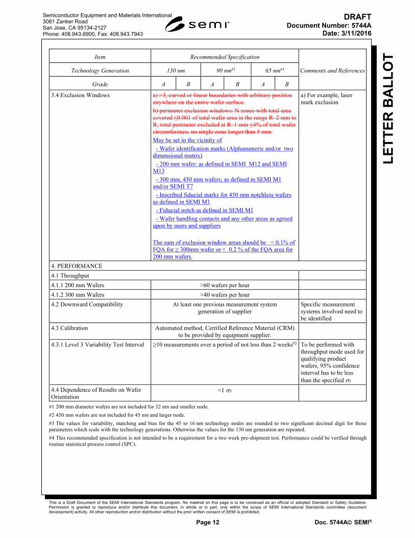
3.4 Exclusion Windows a) >3, curved or linear boundaries with arbitrary position anywhere on the entire wafer surface. b) perimeter exclusion windows: N zones with total area covered ≤0.001 of total wafer area in the range R–2 mm to R, total perimeter excluded at R–1 mm ≤4% of total wafer circumference, no single zone longer than 5 mm. May be set in the vicinity of - Wafer identification marks (Alphanumeric and/or two
dimensional matrix) - 200 mm wafer: as defined in SEMI M12 and SEMI
M13 - 300 mm, 450 mm wafers; as defined in SEMI M1
and/or SEMI T7 - Inscribed fiducial marks for 450 mm notchless wafers
as defined in SEMI M1 - Fiducial notch as defined in SEMI M1 - Wafer handling contacts and any other areas as agreed
upon by users and suppliers The sum of exclusion window areas should be < 0.1% of FQA for ≥ 300mm wafer or < 0.2 % of the FQA area for 200 mm wafers.
a) For example, laser mark exclusion
4. PERFORMANCE
4.1 Throughput
4.1.1 200 mm Wafers >60 wafers per hour
4.1.2 300 mm Wafers >40 wafers per hour
4.2 Downward Compatibility At least one previous measurement system generation of supplier
Specific measurement systems involved need to be identified
4.3 Calibration Automated method, Certified Reference Material (CRM) to be provided by equipment supplier.
4.3.1 Level 3 Variability Test Interval ≥10 measurements over a period of not less than 2 weeks#2 To be performed with throughput mode used for qualifying product wafers, 95% confidence interval has to be less than the specified 3
4.4 Dependence of Results on Wafer Orientation
<1 3
#1 200 mm diameter wafers are not included for 32 nm and smaller node.
#2 450 mm wafers are not included for 45 nm and larger node.
#3 The values for variability, matching and bias for the 45 to 16 nm technology nodes are rounded to two significant decimal digit for those parameters which scale with the technology generations. Otherwise the values for the 130 nm generation are repeated.
#4 This recommended specification is not intended to be a requirement for a two week pre-shipment test. Performance could be verified through routine statistical process control (SPC).
This is a Draft Document of the SEMI International Standards program. No material on this page is to be construed as an official or adopted Standard or Safety Guideline. Permission is granted to reproduce and/or distribute this document, in whole or in part, only within the scope of SEMI International Standards committee (document development) activity. All other reproduction and/or distribution without the prior written consent of SEMI is prohibited.
Page 13 Doc. 5744A SEMI
Semiconductor Equipment and Materials International 3081 Zanker Road San Jose, CA 95134-2127 Phone: 408.943.6900, Fax: 408.943.7943
LE
TT
ER
BA
LL
OT
DRAFTDocument Number: 5744A
Date: 3/11/2016
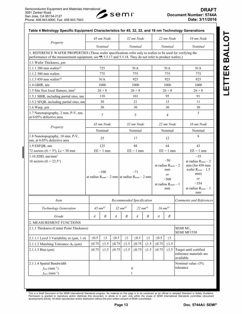
Table 4 Metrology Specific Equipment Characteristics for 45, 32, 22, and 16 nm Technology Generations
Property 45 nm Node 32 nm Node 22 nm Node 16 nm Node
Nominal Nominal Nominal Nominal
1. REFERENCE WAFER PROPERTIES (These wafer specifications refer only to wafers to be used for verifying the performance of the measurement equipment, see ¶¶ 5.5.17 and 5.5.18. They do not refer to product wafers.)
1.1 Wafer Thickness, µm
1.1.1 200 mm wafers#1 725 N/A N/A N/A
1.1.2 300 mm wafers 775 775 775 775
1.1.3 450 mm wafers#2 N/A 925 925 925
1.4 GBIR, nm 1000 1000 1000 1000
1.5 Site Size local flatness, mm2 26 × 8 26 × 8 26 × 8 26 × 8
1.5.1 SBIR, including partial sites, nm 110 101 95 91
1.5.2 SFQR, including partial sites, nm 30 21 15 11
1.6 Warp, µm 30 30 30 30
1.7 Nanotopography, 2 mm, P-V, nm, at 0.05% defective area
7 5 4 3
Property 45 nm Node 32 nm Node 22 nm Node 16 nm Node
Nominal Nominal Nominal Nominal
1.8 Nanotopography, 10 mm, P-V, nm, at 0.05% defective area
25 17 12 8
1.9 ESFQR, nm 72 sectors (θs = 5º), LR = 30 mm
125 EE = 1 mm
88 EE = 1 mm
64 EE = 1 mm
43 EE = 1 mm
1.10 ZDD, nm/mm2 16 sectors (θs = 22.5°)
−100 at radius Rnom – 2 mm
−71 at radius Rnom – 2 mm
−50 at radius Rnom – 2
mm or
−500 at radius Rnom – 1
mm
−35 at radius Rnom – 2 mm (for 450 mm wafer Rnom – 1.5
mm) or
−354 at radius Rnom – 1
mm
Item Recommended Specification Comments and References
Technology Generation 45 nm#3 32 nm#3 22 nm#3 16 nm#3
Grade A B A B A B A B
2. MEASUREMENT FUNCTIONS
2.1.1 Thickness (Center Point Thickness) SEMI M1, SEMI MF1530
2.1.1.1 Level 3 Variability 3 (µm, 1 ) ≤0.5 ≤1 ≤0.5 ≤1 ≤0.5 ≤1 ≤0.5 ≤1
2.1.1.2 Matching Tolerance m (µm) ≤0.75 ≤1.5 ≤0.75 ≤1.5 ≤0.75 ≤1.5 ≤0.75 ≤1.5
2.1.1.3 Bias (µm) ≤0.75 ≤1.5 ≤0.75 ≤1.5 ≤0.75 ≤1.5 ≤0.75 ≤1.5 Target until certified reference materials are available.
2.1.1.4 Spatial Bandwidth fmin (mm–1)
fmax (mm–1)
0 1
Nominal value ±5% tolerance
This is a Draft Document of the SEMI International Standards program. No material on this page is to be construed as an official or adopted Standard or Safety Guideline. Permission is granted to reproduce and/or distribute this document, in whole or in part, only within the scope of SEMI International Standards committee (document development) activity. All other reproduction and/or distribution without the prior written consent of SEMI is prohibited.
Page 14 Doc. 5744A SEMI
Semiconductor Equipment and Materials International 3081 Zanker Road San Jose, CA 95134-2127 Phone: 408.943.6900, Fax: 408.943.7943
LE
TT
ER
BA
LL
OT
DRAFTDocument Number: 5744A
Date: 3/11/2016
Item Recommended Specification Comments and References
Technology Generation 45 nm#3 32 nm#3 22 nm#3 16 nm#3
Grade A B A B A B A B
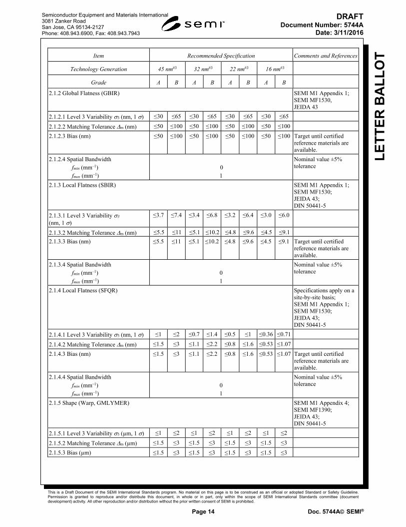
2.1.2 Global Flatness (GBIR) SEMI M1 Appendix 1; SEMI MF1530, JEIDA 43
2.1.2.1 Level 3 Variability 3 (nm, 1 ) ≤30 ≤65 ≤30 ≤65 ≤30 ≤65 ≤30 ≤65
2.1.2.2 Matching Tolerance m (nm) ≤50 ≤100 ≤50 ≤100 ≤50 ≤100 ≤50 ≤100
2.1.2.3 Bias (nm) ≤50 ≤100 ≤50 ≤100 ≤50 ≤100 ≤50 ≤100 Target until certified reference materials are available.
2.1.2.4 Spatial Bandwidth fmin (mm–1)
fmax (mm–1)
0 1
Nominal value ±5% tolerance
2.1.3 Local Flatness (SBIR) SEMI M1 Appendix 1; SEMI MF1530; JEIDA 43; DIN 50441-5
2.1.3.1 Level 3 Variability 3 (nm, 1 )
≤3.7 ≤7.4 ≤3.4 ≤6.8 ≤3.2 ≤6.4 ≤3.0 ≤6.0
2.1.3.2 Matching Tolerance m (nm) ≤5.5 ≤11 ≤5.1 ≤10.2 ≤4.8 ≤9.6 ≤4.5 ≤9.1
2.1.3.3 Bias (nm) ≤5.5 ≤11 ≤5.1 ≤10.2 ≤4.8 ≤9.6 ≤4.5 ≤9.1 Target until certified reference materials are available.
2.1.3.4 Spatial Bandwidth fmin (mm–1)
fmax (mm–1)
0 1
Nominal value ±5% tolerance
2.1.4 Local Flatness (SFQR) Specifications apply on a site-by-site basis; SEMI M1 Appendix 1; SEMI MF1530; JEIDA 43; DIN 50441-5
2.1.4.1 Level 3 Variability 3 (nm, 1 ) ≤1 ≤2 ≤0.7 ≤1.4 ≤0.5 ≤1 ≤0.36 ≤0.71
2.1.4.2 Matching Tolerance m (nm) ≤1.5 ≤3 ≤1.1 ≤2.2 ≤0.8 ≤1.6 ≤0.53 ≤1.07
2.1.4.3 Bias (nm) ≤1.5 ≤3 ≤1.1 ≤2.2 ≤0.8 ≤1.6 ≤0.53 ≤1.07 Target until certified reference materials are available.
2.1.4.4 Spatial Bandwidth fmin (mm–1)
fmax (mm–1)
0 1
Nominal value ±5% tolerance
2.1.5 Shape (Warp, GMLYMER) SEMI M1 Appendix 4; SEMI MF1390; JEIDA 43; DIN 50441-5
2.1.5.1 Level 3 Variability 3 (µm, 1 ) ≤1 ≤2 ≤1 ≤2 ≤1 ≤2 ≤1 ≤2
2.1.5.2 Matching Tolerance m (µm) ≤1.5 ≤3 ≤1.5 ≤3 ≤1.5 ≤3 ≤1.5 ≤3
2.1.5.3 Bias (µm) ≤1.5 ≤3 ≤1.5 ≤3 ≤1.5 ≤3 ≤1.5 ≤3
This is a Draft Document of the SEMI International Standards program. No material on this page is to be construed as an official or adopted Standard or Safety Guideline. Permission is granted to reproduce and/or distribute this document, in whole or in part, only within the scope of SEMI International Standards committee (document development) activity. All other reproduction and/or distribution without the prior written consent of SEMI is prohibited.
Page 15 Doc. 5744A SEMI
Semiconductor Equipment and Materials International 3081 Zanker Road San Jose, CA 95134-2127 Phone: 408.943.6900, Fax: 408.943.7943
LE
TT
ER
BA
LL
OT
DRAFTDocument Number: 5744A
Date: 3/11/2016
Item Recommended Specification Comments and References
Technology Generation 45 nm#3 32 nm#3 22 nm#3 16 nm#3
Grade A B A B A B A B
2.1.5.4 Spatial Bandwidth fmin (mm–1)
fmax (mm–1)
0 1
Nominal value ±5% tolerance
2.1.6 Other Global Flatness Parameters SEMI M1 Appendix 1; SEMI MF1530; JEIDA 43; DIN 50441-5
2.1.6.1 GFLR, GFLD required
2.1.7 Other Local Flatness Parameters SEMI M1 Appendix 1; SEMI MF1530; JEIDA 43; DIN 50441-5
2.1.7.1 SBID, SFLR, SFLD, SFQD, SFSR, SFSD
required
2.1.8 Other Shape Parameters SEMI M1 Appendix 4; SEMI MF1390; JEIDA 43; DIN 50441-5
2.1.8.1 Sori (GFLYFER), Bow (GM3YMCD), Warp (GB3NMPR)
required
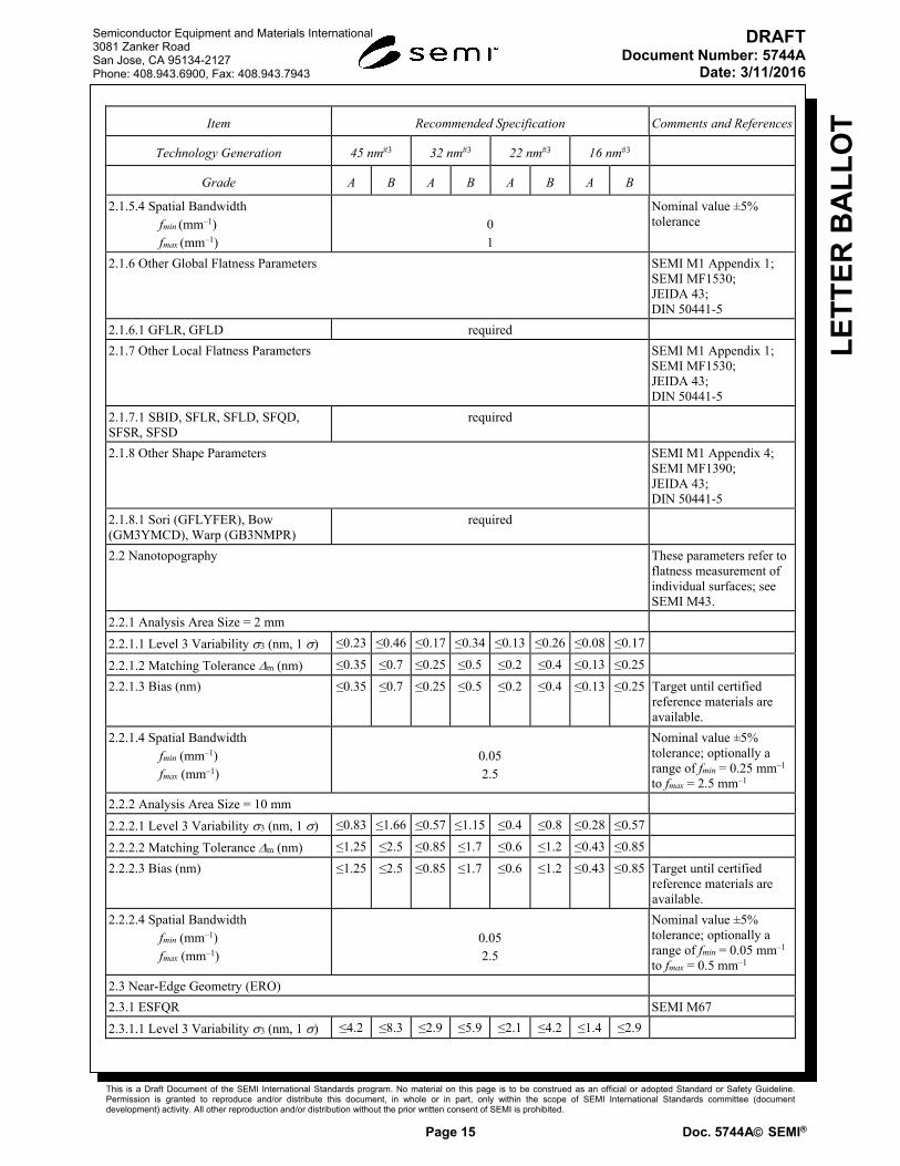
2.2 Nanotopography These parameters refer to flatness measurement of individual surfaces; see SEMI M43.
2.2.1 Analysis Area Size = 2 mm
2.2.1.1 Level 3 Variability 3 (nm, 1 ) ≤0.23 ≤0.46 ≤0.17 ≤0.34 ≤0.13 ≤0.26 ≤0.08 ≤0.17
2.2.1.2 Matching Tolerance m (nm) ≤0.35 ≤0.7 ≤0.25 ≤0.5 ≤0.2 ≤0.4 ≤0.13 ≤0.25
2.2.1.3 Bias (nm) ≤0.35 ≤0.7 ≤0.25 ≤0.5 ≤0.2 ≤0.4 ≤0.13 ≤0.25 Target until certified reference materials are available.
2.2.1.4 Spatial Bandwidth fmin (mm–1)
fmax (mm–1)
0.05 2.5
Nominal value ±5% tolerance; optionally a range of fmin = 0.25 mm–1 to fmax = 2.5 mm–1
2.2.2 Analysis Area Size = 10 mm
2.2.2.1 Level 3 Variability 3 (nm, 1 ) ≤0.83 ≤1.66 ≤0.57 ≤1.15 ≤0.4 ≤0.8 ≤0.28 ≤0.57
2.2.2.2 Matching Tolerance m (nm) ≤1.25 ≤2.5 ≤0.85 ≤1.7 ≤0.6 ≤1.2 ≤0.43 ≤0.85
2.2.2.3 Bias (nm) ≤1.25 ≤2.5 ≤0.85 ≤1.7 ≤0.6 ≤1.2 ≤0.43 ≤0.85 Target until certified reference materials are available.
2.2.2.4 Spatial Bandwidth fmin (mm–1)
fmax (mm–1)
0.05 2.5
Nominal value ±5% tolerance; optionally a range of fmin = 0.05 mm–1 to fmax = 0.5 mm–1
2.3 Near-Edge Geometry (ERO)
2.3.1 ESFQR SEMI M67
2.3.1.1 Level 3 Variability 3 (nm, 1 ) ≤4.2 ≤8.3 ≤2.9 ≤5.9 ≤2.1 ≤4.2 ≤1.4 ≤2.9
This is a Draft Document of the SEMI International Standards program. No material on this page is to be construed as an official or adopted Standard or Safety Guideline. Permission is granted to reproduce and/or distribute this document, in whole or in part, only within the scope of SEMI International Standards committee (document development) activity. All other reproduction and/or distribution without the prior written consent of SEMI is prohibited.
Page 16 Doc. 5744A SEMI
Semiconductor Equipment and Materials International 3081 Zanker Road San Jose, CA 95134-2127 Phone: 408.943.6900, Fax: 408.943.7943
LE
TT
ER
BA
LL
OT
DRAFTDocument Number: 5744A
Date: 3/11/2016
Item Recommended Specification Comments and References
Technology Generation 45 nm#3 32 nm#3 22 nm#3 16 nm#3
Grade A B A B A B A B
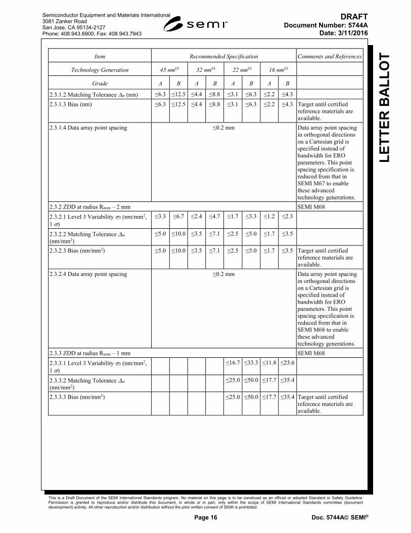
2.3.1.2 Matching Tolerance m (nm) ≤6.3 ≤12.5 ≤4.4 ≤8.8 ≤3.1 ≤6.3 ≤2.2 ≤4.3
2.3.1.3 Bias (nm) ≤6.3 ≤12.5 ≤4.4 ≤8.8 ≤3.1 ≤6.3 ≤2.2 ≤4.3 Target until certified reference materials are available.
2.3.1.4 Data array point spacing ≤0.2 mm Data array point spacing in orthogonal directions on a Cartesian grid is specified instead of bandwidth for ERO parameters. This point spacing specification is reduced from that in SEMI M67 to enable these advanced technology generations.
2.3.2 ZDD at radius Rnom – 2 mm SEMI M68
2.3.2.1 Level 3 Variability 3 (nm/mm2, 1 )
≤3.3 ≤6.7 ≤2.4 ≤4.7 ≤1.7 ≤3.3 ≤1.2 ≤2.3
2.3.2.2 Matching Tolerance m (nm/mm2)
≤5.0 ≤10.0 ≤3.5 ≤7.1 ≤2.5 ≤5.0 ≤1.7 ≤3.5
2.3.2.3 Bias (nm/mm2) ≤5.0 ≤10.0 ≤3.5 ≤7.1 ≤2.5 ≤5.0 ≤1.7 ≤3.5 Target until certified reference materials are available.
2.3.2.4 Data array point spacing ≤0.2 mm Data array point spacing in orthogonal directions on a Cartesian grid is specified instead of bandwidth for ERO parameters. This point spacing specification is reduced from that in SEMI M68 to enable these advanced technology generations.
2.3.3 ZDD at radius Rnom – 1 mm SEMI M68
2.3.3.1 Level 3 Variability 3 (nm/mm2, 1 )
≤16.7 ≤33.3 ≤11.8 ≤23.6
2.3.3.2 Matching Tolerance m (nm/mm2)
≤25.0 ≤50.0 ≤17.7 ≤35.4
2.3.3.3 Bias (nm/mm2) ≤25.0 ≤50.0 ≤17.7 ≤35.4 Target until certified reference materials are available.

This is a Draft Document of the SEMI International Standards program. No material on this page is to be construed as an official or adopted Standard or Safety Guideline. Permission is granted to reproduce and/or distribute this document, in whole or in part, only within the scope of SEMI International Standards committee (document development) activity. All other reproduction and/or distribution without the prior written consent of SEMI is prohibited.
Page 17 Doc. 5744A SEMI
Semiconductor Equipment and Materials International 3081 Zanker Road San Jose, CA 95134-2127 Phone: 408.943.6900, Fax: 408.943.7943
LE
TT
ER
BA
LL
OT
DRAFTDocument Number: 5744A
Date: 3/11/2016
Item Recommended Specification Comments and References
Technology Generation 45 nm#3 32 nm#3 22 nm#3 16 nm#3
Grade A B A B A B A B
2.3.3.4 Data array point spacing ≤0.2 mm Data array point spacing in orthogonal directions on a Cartesian grid is specified instead of bandwidth for ERO parameters. This point spacing specification is reduced from that in SEMI M68 to enable these advanced technology generations.
2.3.4 Other ERO Parameters user specific
2.4 Other Parameters
2.4.1 Waviness user specific
2.4.2 Height (individual wafer surfaces)
user specific
2.4.3 Slope user specific
2.4.4 Curvature user specific
2.4.5 Line Scans user specific
2.4.6 Contour Maps user specific
2.4.7 Data Histogram 10 or more bins per channel, arbitrarily definable, cumulative differential
2.4.8 Additional Parameters user specific
3. SETUP PARAMETERS
3.1 Nominal Edge Exclusion defining FQA (mm)
3.1.1 All Parameters except Near-Edge Geometry (ERO)
≥1.5 ≥1.5 ≥1.5 ≥1.5 Performance parameters are to be verified with nominal edge exclusion ≥2 mm or ≥1.5 mm for 450 mm wafers. Instrument must be capable of reporting to nominal edge exclusion ≥1 mm. As a guide, the extended performance for nominal edge exclusion <2 mm or <1.5 mm for 450 mm wafers should not exceed the performance (3, matching, bias) by more than 100% as compared to ≥2 mm or ≥1.5 mm for 450 mm wafers edge exclusion given appropriate reference material.
This is a Draft Document of the SEMI International Standards program. No material on this page is to be construed as an official or adopted Standard or Safety Guideline. Permission is granted to reproduce and/or distribute this document, in whole or in part, only within the scope of SEMI International Standards committee (document development) activity. All other reproduction and/or distribution without the prior written consent of SEMI is prohibited.
Page 18 Doc. 5744A SEMI
Semiconductor Equipment and Materials International 3081 Zanker Road San Jose, CA 95134-2127 Phone: 408.943.6900, Fax: 408.943.7943
LE
TT
ER
BA
LL
OT
DRAFTDocument Number: 5744A
Date: 3/11/2016
Item Recommended Specification Comments and References
Technology Generation 45 nm#3 32 nm#3 22 nm#3 16 nm#3
Grade A B A B A B A B
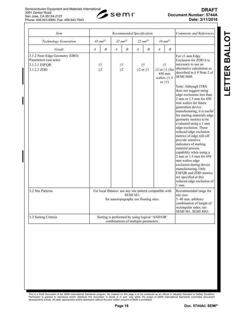
3.1.2 Near-Edge Geometry (ERO) Parameters (see note) 3.1.2.1 ESFQR 3.1.2.2 ZDD
≥1 ≥2
≥1 ≥2
≥1 ≥2 or ≥1
≥1 ≥2 or ≥1 (for
450 mm wafers ≥1.5
or ≥1)
For 1 mm Edge Exclusion for ZDD it is necessary to use an alternative calculation as described in § 9 Note 2 of SEMI M68. Note: Although ITRS does not suggest using edge exclusions less than 2 mm or 1.5 mm for 450 mm wafers for future generation device manufacturing, it is useful for starting materials edge geometry metrics to be evaluated using a 1 mm edge exclusion. These reduced edge exclusion metrics of edge roll-off provide sensitive indicators of starting material process capability when using a 2 mm or 1.5 mm for 450 mm wafers edge exclusion during device manufacturing. Only ESFQR and ZDD metrics are specified at this reduced edge exclusion of 1 mm.
3.2 Site Patterns For local flatness: use any site pattern compatible with SEMI M1;
for nanotopography use floating sites.
Recommended range for site size: 5–40 mm, arbitrary combination of length of rectangular sides; see SEMI M1, SEMI M43.
3.3 Sorting Criteria Sorting is performed by using logical ‘AND/OR’ combinations of multiple parameters.
This is a Draft Document of the SEMI International Standards program. No material on this page is to be construed as an official or adopted Standard or Safety Guideline. Permission is granted to reproduce and/or distribute this document, in whole or in part, only within the scope of SEMI International Standards committee (document development) activity. All other reproduction and/or distribution without the prior written consent of SEMI is prohibited.
Page 19 Doc. 5744A SEMI
Semiconductor Equipment and Materials International 3081 Zanker Road San Jose, CA 95134-2127 Phone: 408.943.6900, Fax: 408.943.7943
LE
TT
ER
BA
LL
OT
DRAFTDocument Number: 5744A
Date: 3/11/2016
Item Recommended Specification Comments and References
Technology Generation 45 nm#3 32 nm#3 22 nm#3 16 nm#3
Grade A B A B A B A B
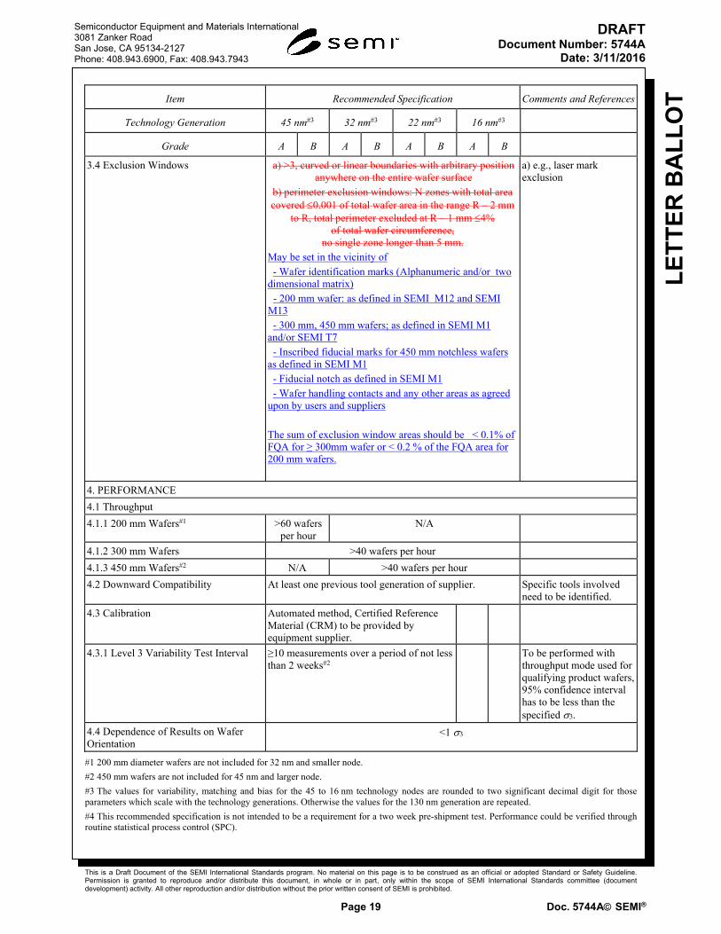
3.4 Exclusion Windows a) >3, curved or linear boundaries with arbitrary position anywhere on the entire wafer surface
b) perimeter exclusion windows: N zones with total area covered 0.001 of total wafer area in the range R – 2 mm
to R, total perimeter excluded at R – 1 mm 4% of total wafer circumference,
no single zone longer than 5 mm. May be set in the vicinity of - Wafer identification marks (Alphanumeric and/or two
dimensional matrix) - 200 mm wafer: as defined in SEMI M12 and SEMI
M13 - 300 mm, 450 mm wafers; as defined in SEMI M1
and/or SEMI T7 - Inscribed fiducial marks for 450 mm notchless wafers
as defined in SEMI M1 - Fiducial notch as defined in SEMI M1 - Wafer handling contacts and any other areas as agreed
upon by users and suppliers The sum of exclusion window areas should be < 0.1% of FQA for ≥ 300mm wafer or < 0.2 % of the FQA area for 200 mm wafers.
a) e.g., laser mark exclusion
4. PERFORMANCE
4.1 Throughput
4.1.1 200 mm Wafers#1 >60 wafers per hour
N/A
4.1.2 300 mm Wafers >40 wafers per hour
4.1.3 450 mm Wafers#2 N/A >40 wafers per hour
4.2 Downward Compatibility At least one previous tool generation of supplier. Specific tools involved need to be identified.
4.3 Calibration Automated method, Certified Reference Material (CRM) to be provided by equipment supplier.
4.3.1 Level 3 Variability Test Interval ≥10 measurements over a period of not less than 2 weeks#2
To be performed with throughput mode used for qualifying product wafers, 95% confidence interval has to be less than the specified 3.
4.4 Dependence of Results on Wafer Orientation
<1 3
#1 200 mm diameter wafers are not included for 32 nm and smaller node.
#2 450 mm wafers are not included for 45 nm and larger node.
#3 The values for variability, matching and bias for the 45 to 16 nm technology nodes are rounded to two significant decimal digit for those parameters which scale with the technology generations. Otherwise the values for the 130 nm generation are repeated.
#4 This recommended specification is not intended to be a requirement for a two week pre-shipment test. Performance could be verified through routine statistical process control (SPC).

This is a Draft Document of the SEMI International Standards program. No material on this page is to be construed as an official or adopted Standard or Safety Guideline. Permission is granted to reproduce and/or distribute this document, in whole or in part, only within the scope of SEMI International Standards committee (document development) activity. All other reproduction and/or distribution without the prior written consent of SEMI is prohibited.
Page 20 Doc. 5744A SEMI
Semiconductor Equipment and Materials International 3081 Zanker Road San Jose, CA 95134-2127 Phone: 408.943.6900, Fax: 408.943.7943
LE
TT
ER
BA
LL
OT
DRAFTDocument Number: 5744A
Date: 3/11/2016
Table 5 Metrology Specific Equipment Characteristics for Edge Profile Measurement#1
Property Nominal Range
This is a Draft Document of the SEMI International Standards program. No material on this page is to be construed as an official or adopted Standard or Safety Guideline. Permission is granted to reproduce and/or distribute this document, in whole or in part, only within the scope of SEMI International Standards committee (document development) activity. All other reproduction and/or distribution without the prior written consent of SEMI is prohibited.
Page 21 Doc. 5744A SEMI
Semiconductor Equipment and Materials International 3081 Zanker Road San Jose, CA 95134-2127 Phone: 408.943.6900, Fax: 408.943.7943
LE
TT
ER
BA
LL
OT
DRAFTDocument Number: 5744A
Date: 3/11/2016
APPENDIX 1 SCALING MODELS
NOTICE: The material in this Appendix is an official part of SEMI M49 and was approved by full letter ballot procedures on June 4, 2013.
SEMI makes no warranties or representations as to the suitability of the Standards and Safety Guidelines set forth herein for any particular application. The determination of the suitability of the Standard or Safety Guideline is solely the responsibility of the user. Users are cautioned to refer to manufacturer’s instructions, product labels, product data sheets, and other relevant literature, respecting any materials or equipment mentioned herein. Standards and Safety Guidelines are subject to change without notice.
The user’s attention is called to the possibility that compliance with this Standard or Safety Guideline may require use of copyrighted material or of an invention covered by patent rights. KLA-Tencor has filed a statement with SEMI asserting that licenses will be made available to applicants throughout the world for the purpose of implementing this Standard or Safety Guideline without unfair discrimination. Attention is also drawn to the possibility that some elements of this Standard or Safety Guideline may be subject to patented technology or copyrighted items other than those identified above. SEMI shall not be held responsible for identifying any or all such patented technology or copyrighted items. By publication of this Standard or Safety Guideline, SEMI takes no position respecting the validity of any patent rights or copyrights asserted in connection with any item mentioned in this Standard or Safety Guideline. Users of this Standard or Safety Guideline are expressly advised that determination of any such patent rights or copyrights and the risk of infringement of such rights are entirely their own responsibility.