Lagrangian dynamics of the Mistral during the HyMeX SOP2 ...
AZ 1512 RESIST PHOTOLITHOGRAPHY STANDARD OPERATIONAL PROCEDURES
Bonghoe Kim
EE527 SPRING 2011
SUPERVISOR: PROFESSOR DARLING, R BRUCE
MAY 9, 2011
Department of Electrical Engineering
University of Wahsington
BONGHOE KIM
EE527 SPRING 2011
SUPERVISOR: PROFESSOR DARLING, R BRUCE
MAY 9, 2011
AZ 1512 RESIST PHOTOLITHOGRAPHY 1
AZ 1512 RESIST PHOTOLITHOGRAPHY
STANDARD OPERATIONAL
PROCEDURES
Part I. Experiment Environment
Basic Information
-Laboratory Information: Microfabrication
Laboratory (Room# EEB B025, Electrical
Engineering Building, University of
Washington).
-Emergency Contact: Prof. R. Bruce Darling ([email protected], (206) 543-4707,
226 EEB)
Equipment and Personal Safety Protectors
[Equipment & Protectors]
# Process Step Equipment Use Limitation of Material
Protectors
(For Samples,
For personal)
1 Dehydration Baking Hot plate Fit 3 inch Glass plate Latex Gloves
2 Photoresist Coating Spin-coater Maximum 4 inch wafer Latex Gloves
3 Pre-Baking Hot plate Fit 3 inch Glass plate Latex Gloves
4 Alignment Oriel Aligner Maximum 3 inch wafer Latex Gloves
5 UV-Exposure Oriel Aligner Maximum 3 inch wafer Latex Gloves
6 Development Fume Hood System - Full-face Mask,
Apron, Gloves
7 Post-Baking Hot plate Fit 3 inch Glass plate Latex Gloves
AZ 1512 RESIST PHOTOLITHOGRAPHY 2
8 Inspection Microscope - Latex Gloves
-Limitations of Wafer size: Because of limitations of equipment’s capability, wafer size
should be specified for the each process step.
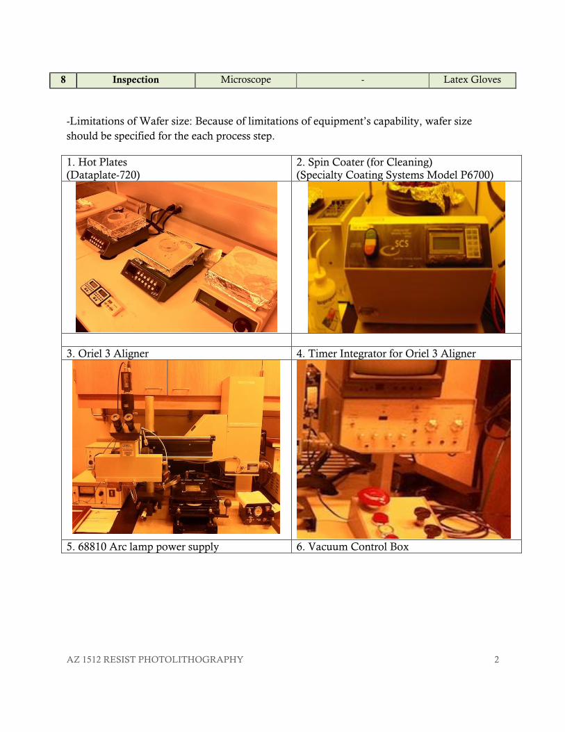
1. Hot Plates
(Dataplate-720)
2. Spin Coater (for Cleaning)
(Specialty Coating Systems Model P6700)
3. Oriel 3 Aligner 4. Timer Integrator for Oriel 3 Aligner
5. 68810 Arc lamp power supply 6. Vacuum Control Box
AZ 1512 RESIST PHOTOLITHOGRAPHY 3
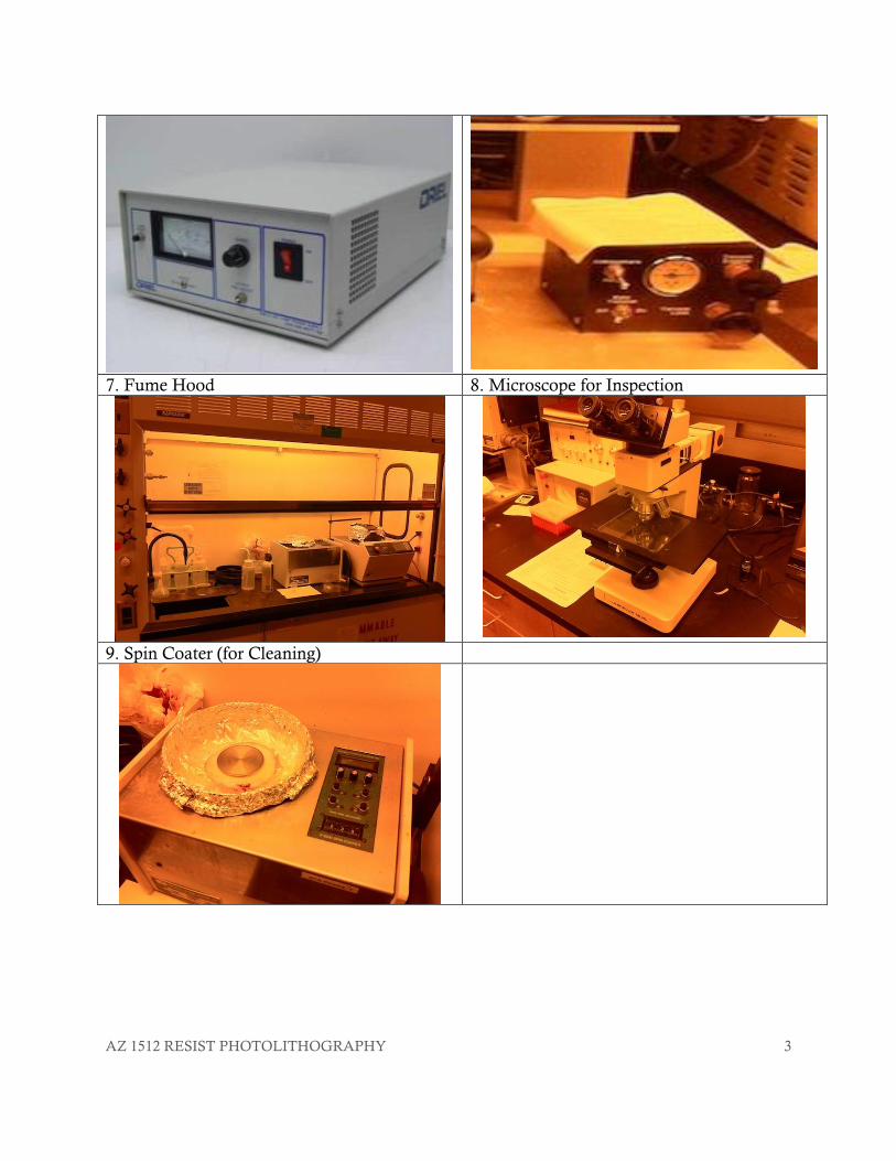
7. Fume Hood 8. Microscope for Inspection
9. Spin Coater (for Cleaning)
AZ 1512 RESIST PHOTOLITHOGRAPHY 4
Materials Preparation
[Materials]
-Chemical Materials:
# Materials Purpose Cautions for handling
1 AZ 1512
PHOTORESIST Coating material
Keep the PR bottle clean.
Waste an extra PR in the pipette.
2 AZ 300 MIF
DEVELOPER Removing PR exposed -
3 3 inch Glass Plate Keep Uniform temperature -
4 DI Water Cleaning Use the DI water with over ~17Mohm
to insure quality and electrical features.
5 Acetone Remove Photoresist
Flammable solvent, Keep away from
fire and high temp.
Use the Fume Hood System.
6 Isopropanol Remove remain Acetone -
Expected Hazards & Cautions (at each process step)
# Process Step Hazard
Cause Effect
1 Dehydration Baking High Temperature Burn of Skin
2 Photoresist Coating No vacuum holding Break wafer
Inhalation Carcinogen, blood poison
3 Pre-Baking High Temperature Burn of Skin
4 Alignment Drop mask mount hold cover Break Mask
5 UV-Exposure
UV Exposure
Wrong high voltage cable
connection
Burn of Eyes and Skin
Sparks and explosion
6 Development - -
7 Post-Baking High Temperature Burn of Skin
8 Inspection Let the Lenz hit the sample Scratch the surface of sample

AZ 1512 RESIST PHOTOLITHOGRAPHY 5
Part II. Operational Procedures (Photolithography)
Introduction
- Photolithography is one of processes used in micro-fabrication work to remove area that is
not needed on a thin film surface or the substrate bulk. It uses light, such as UV, to transfer
a geometric pattern from a photo mask to a light-sensitive chemical "photoresist". AZ 1512
series positive photoresists are established for i, h, and g-line; UV spectrum 310nm ~ 440nm
and broadband resists. AZ 1512 Photoresist can be developed in AZ 300 MIF developers.
The purpose of this Standard Operational Procedure (SOP) is to be directions for high-
efficient Lab process as well as a practical method of laboratory R&D documentation.
STEP 1. Dehydration Baking
- This step is to remove humidity on the surface of substrate. For this step, Hot Plates or
Convection oven can be employed. Equipment 1 as shown above, page 2, is used
dehydration step.
Dehydration Baking
# Process Stages Detailed Actions
1 Turn on the Hot Plate Switch 1. Turn on switch
2 Setting the Temperature of Hot Plate
1. Press ENT
2. Press Plate Temperature
3. Type Desired Temperature 95 deg. C.
4. Press ENT
** Desired Temperature: You should consider
temperature loss by 3-inch Glass Plate (grinded
both sides to get very smooth surface). Type 5
deg. C more temp.
5. Check temperature with Handy Surface
Thermometer.
6. Check the temperature at several points (see
picture below)
7. Q: Is Thermometer indicating the Exact
Temperature you want?
YES (go to next stage)
NO (go to number 2-1)
AZ 1512 RESIST PHOTOLITHOGRAPHY 6
3 Set up Timer 1. Type 6,0 (for 60 sec) or 1,0,0 (for 1min.)
4 Place the wafer and press start button
on Timer
1. Place the wafer very carefully. (Glass surface is
very smooth, so, the wafer is easy to slip.)
[Simultaneously]
1. Press Start Button on Timer
5 Timer is ringing! Turn off
6 Remove the wafer from the Hot Plate
1. Remove the wafer very carefully.
2. Place the wafer glass slide (for cooling)
3. Cover the wafer (To protect from particles)
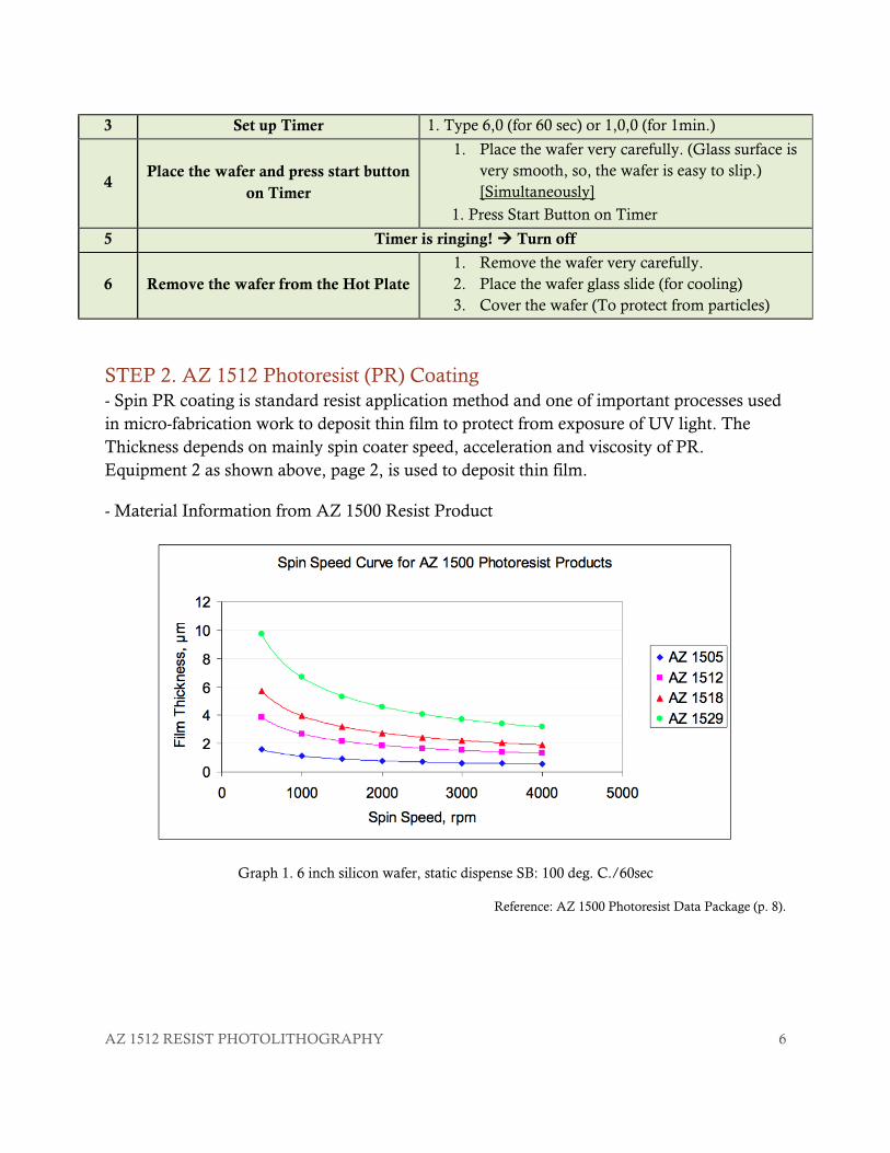
STEP 2. AZ 1512 Photoresist (PR) Coating
- Spin PR coating is standard resist application method and one of important processes used
in micro-fabrication work to deposit thin film to protect from exposure of UV light. The
Thickness depends on mainly spin coater speed, acceleration and viscosity of PR.
Equipment 2 as shown above, page 2, is used to deposit thin film.
- Material Information from AZ 1500 Resist Product
Graph 1. 6 inch silicon wafer, static dispense SB: 100 deg. C./60sec
Reference: AZ 1500 Photoresist Data Package (p. 8).
AZ 1512 RESIST PHOTOLITHOGRAPHY 7
AZ 1512 Photoresist (PR) Coating
# Process Stages Detailed Actions
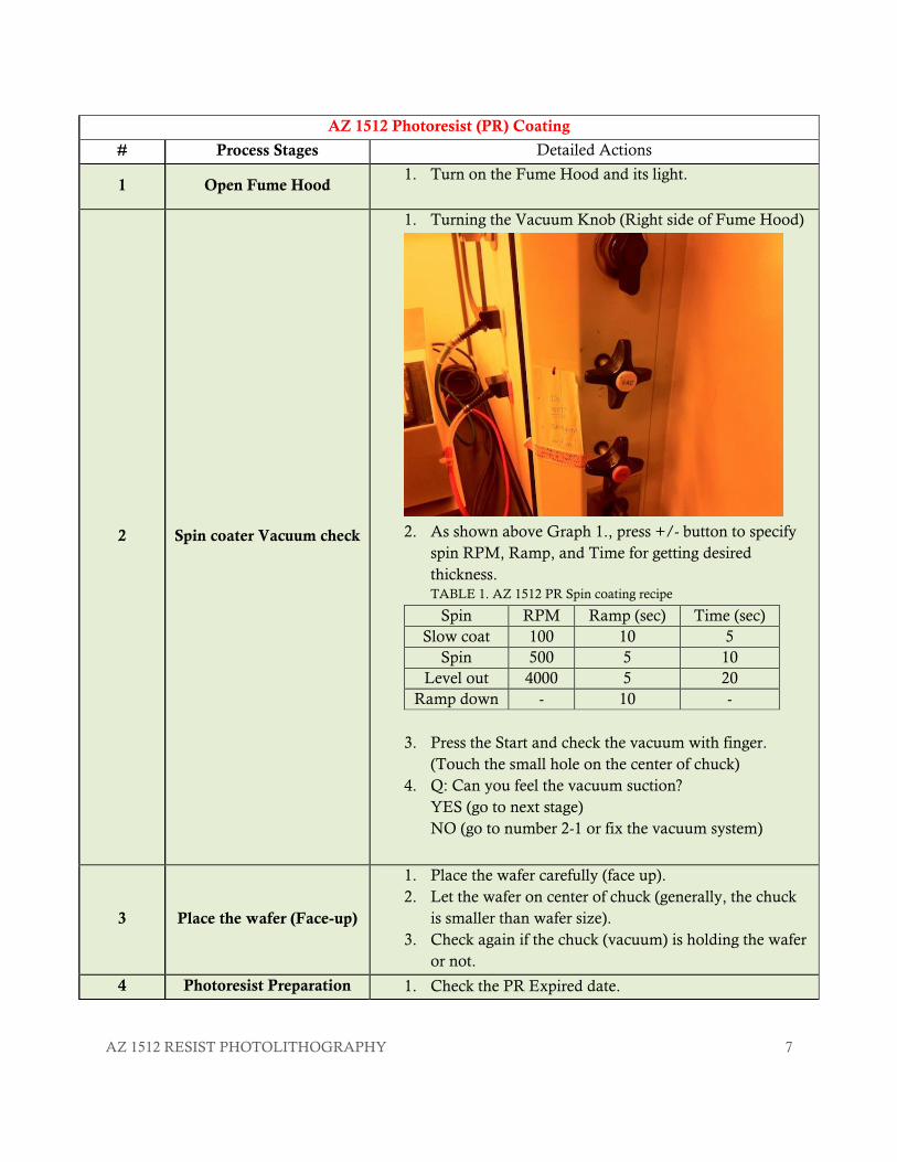
1 Open Fume Hood 1. Turn on the Fume Hood and its light.
2 Spin coater Vacuum check
1. Turning the Vacuum Knob (Right side of Fume Hood)
2. As shown above Graph 1., press +/- button to specify
spin RPM, Ramp, and Time for getting desired
thickness.
TABLE 1. AZ 1512 PR Spin coating recipe
Spin RPM Ramp (sec) Time (sec)
Slow coat 100 10 5
Spin 500 5 10
Level out 4000 5 20
Ramp down - 10 -
3. Press the Start and check the vacuum with finger.
(Touch the small hole on the center of chuck)
4. Q: Can you feel the vacuum suction?
YES (go to next stage)
NO (go to number 2-1 or fix the vacuum system)
3 Place the wafer (Face-up)
1. Place the wafer carefully (face up).
2. Let the wafer on center of chuck (generally, the chuck
is smaller than wafer size).
3. Check again if the chuck (vacuum) is holding the wafer
or not.
4 Photoresist Preparation 1. Check the PR Expired date.
AZ 1512 RESIST PHOTOLITHOGRAPHY 8
2. With using pipette, drop the PR material on the silicon
surface carefully to avoid PR bubbles. Also, PR should
be appropriate amount so that surplus PR does not
stain it.
3. Pipette must not be dipped.
4. [Remain PR] Remain PR should be wasted on
aluminum foil around the chuck of spin coater.
5. [PR Bubble] Get rid of PR bubbles from the center of
the wafer surface to the edge.
5 Start PR Spin coating 1. Press the start button to start spin coater.
6 Remove the wafer &
check
1. Turn off the vacuum (Stop button) to remove the wafer
from the chuck.
2. Check the deposited PR condition with Microscope.
3. Q: Is the PR coating acceptable?
YES (go to next stage)
NO (go to number 6-recover)
6-recover Strip deposited PR
1. Pour appropriate amount acetone in a Schale or a
beaker.
2. Soak the wafer (use Scooping motion) and then agitate
it (about 40 sec.).
3. Remove the acetone with the spin coater. (Isopropanol)
4. Clean water again with DI water (over ~17Mohm).
5. Dry the backside of wafer.
6. Inspection with Microscope.
7. Q: Is the PR removed appropriately?
YES (go to next stage)
NO (go to number 6-recover)
STEP 3. Pre-Baking
- The purpose of this step is to remove the solvent from photoresist. Also, this step make the
deposited photoresist adhere to the wafer surface well.
Pre-Baking
# Process Stages Detailed Actions

AZ 1512 RESIST PHOTOLITHOGRAPHY 9
1 Turn on the Hot Plate Switch 1. You do not need to change the setting
condition because the Hot Plate is already set
up in 1st step.
2 Setting the Temperature of Hot Plate
3 Set up Timer
4 Place the wafer and press start button
on Timer
5 Timer is ringing! Turn off
6 Remove the wafer from the Hot Plate
1. Remove the wafer very carefully.
2. Place the wafer glass slide (for cooling)
3. Cover the wafer (To protect from particles)
STEP 4. Alignment & Exposure (Oriel 3 Aligner)
- The purpose of this step is to change the molecular form of selected area of the PR-coated
substrate. Endurance and carefulness is highly required for this step in order to minimize
misaligns that have influence on electrical characteristics of device. UV-radiation will be
used as light source.
Alignment & Exposure (Oriel 3 Aligner)
# Process Stages Detailed Actions
1 Warm-up Alignment &
Exposure machine
1. Turn on the UV-light power supply and press start and
wait until the UV-light source is stabilized.
2 Mask Alignment
1. Turning the Vacuum Knob (Right side of Fume Hood)
5. Source Specifications:
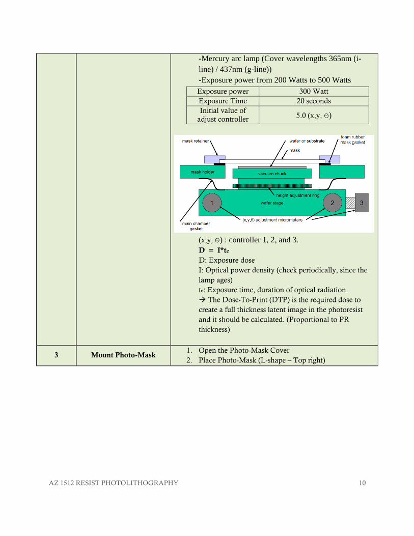
AZ 1512 RESIST PHOTOLITHOGRAPHY 10
-Mercury arc lamp (Cover wavelengths 365nm (i-
line) / 437nm (g-line))
-Exposure power from 200 Watts to 500 Watts
Exposure power 300 Watt
Exposure Time 20 seconds
Initial value of
adjust controller 5.0 (x,y, Θ)
(x,y, Θ) : controller 1, 2, and 3.
D = I*te
D: Exposure dose
I: Optical power density (check periodically, since the
lamp ages)
te: Exposure time, duration of optical radiation.
The Dose-To-Print (DTP) is the required dose to
create a full thickness latent image in the photoresist
and it should be calculated. (Proportional to PR
thickness)
3 Mount Photo-Mask 1. Open the Photo-Mask Cover
2. Place Photo-Mask (L-shape – Top right)
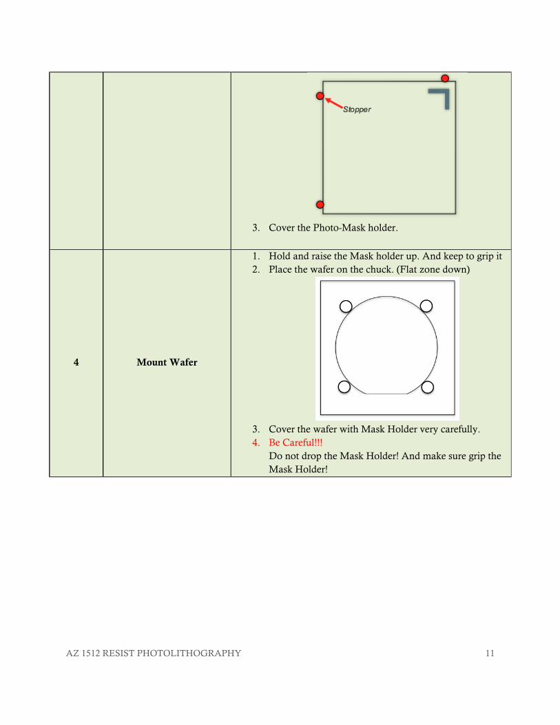
AZ 1512 RESIST PHOTOLITHOGRAPHY 11
3. Cover the Photo-Mask holder.
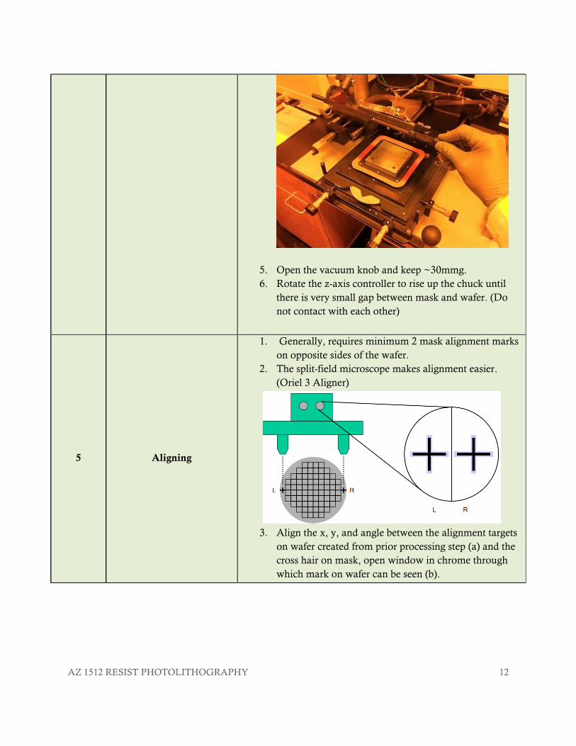
4 Mount Wafer
1. Hold and raise the Mask holder up. And keep to grip it
2. Place the wafer on the chuck. (Flat zone down)
3. Cover the wafer with Mask Holder very carefully.
4. Be Careful!!!
Do not drop the Mask Holder! And make sure grip the
Mask Holder!
AZ 1512 RESIST PHOTOLITHOGRAPHY 12
5. Open the vacuum knob and keep ~30mmg.
6. Rotate the z-axis controller to rise up the chuck until
there is very small gap between mask and wafer. (Do
not contact with each other)
5 Aligning
1. Generally, requires minimum 2 mask alignment marks
on opposite sides of the wafer.
2. The split-field microscope makes alignment easier.
(Oriel 3 Aligner)
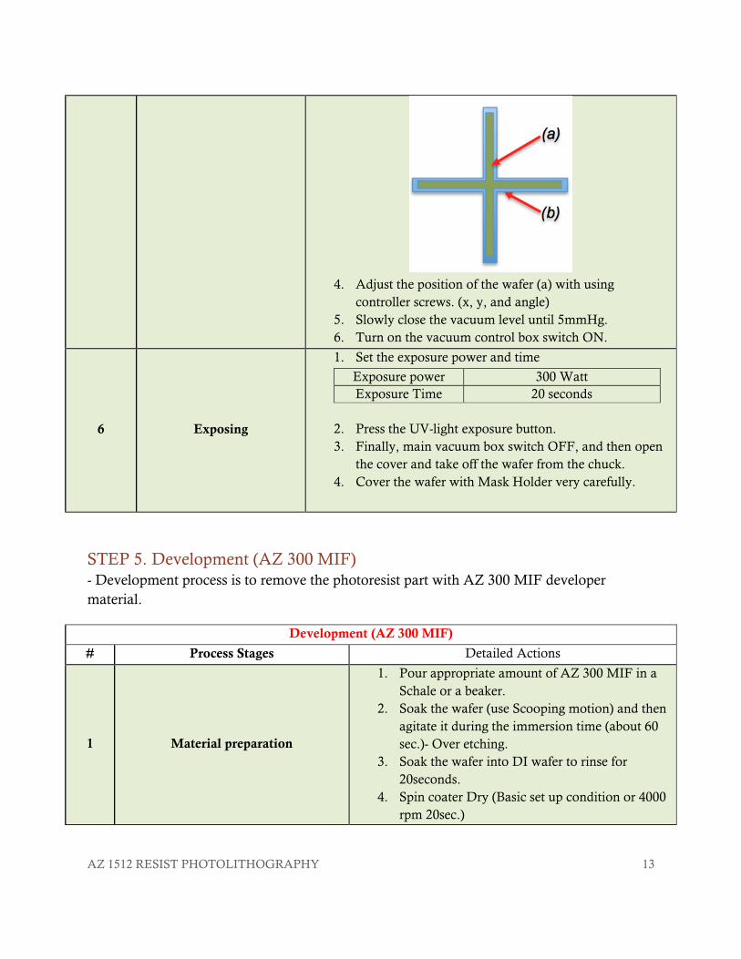
3. Align the x, y, and angle between the alignment targets
on wafer created from prior processing step (a) and the
cross hair on mask, open window in chrome through
which mark on wafer can be seen (b).
AZ 1512 RESIST PHOTOLITHOGRAPHY 13
4. Adjust the position of the wafer (a) with using
controller screws. (x, y, and angle)
5. Slowly close the vacuum level until 5mmHg.
6. Turn on the vacuum control box switch ON.
6 Exposing
1. Set the exposure power and time
Exposure power 300 Watt
Exposure Time 20 seconds
2. Press the UV-light exposure button.
3. Finally, main vacuum box switch OFF, and then open
the cover and take off the wafer from the chuck.
4. Cover the wafer with Mask Holder very carefully.
STEP 5. Development (AZ 300 MIF)
- Development process is to remove the photoresist part with AZ 300 MIF developer
material.
Development (AZ 300 MIF)
# Process Stages Detailed Actions
1 Material preparation
1. Pour appropriate amount of AZ 300 MIF in a
Schale or a beaker.
2. Soak the wafer (use Scooping motion) and then
agitate it during the immersion time (about 60
sec.)- Over etching.
3. Soak the wafer into DI wafer to rinse for
20seconds.
4. Spin coater Dry (Basic set up condition or 4000
rpm 20sec.)

AZ 1512 RESIST PHOTOLITHOGRAPHY 14
5. Dry backside with Air spray.(Red Screw-
Middle one)
6. Inspection with Microscope.
7. Q: Is the PR removed appropriately?
YES (go to next stage)
NO (go to number 1-1)
STEP 6. Post-Baking
- The purpose of this step is to stabilize and solidify the photoresist undeveloped. With using
Hot Plate, post baking process will be achieved by specified condition.
Post-Baking
# Process Stages Detailed Actions
1 Turn on the Hot Plate Switch 1. You do not need to change the setting
condition because the Hot Plate is already set
up in 1st step.
2 Setting the Temperature of Hot Plate
3 Set up Timer
4 Place the wafer and press start button
on Timer
5 Timer is ringing! Turn off
6 Remove the wafer from the Hot Plate
4. Remove the wafer very carefully.
5. Place the wafer glass slide (for cooling)
6. Cover the wafer (To protect from particles)

AZ 1512 RESIST PHOTOLITHOGRAPHY 15
STEP 7. Stripping photoresist
- The photoresist on the wafer should be removed with solvent materials; Acetone. And
Then DI water rinse will be achieved. Finally, Inspection process will be performed to check
the conditions of process.
Stripping photoresist
# Process Stages Detailed Actions
1 Strip deposited PR
8. Pour appropriate amount acetone in a Schale or
a beaker.
9. Soak the wafer (use Scooping motion) and then
agitate it (about 40 sec.).
10. Remove the acetone with the spin coater.
(Isopropanol)
11. Clean water again with DI water (over
~17Mohm).
12. Dry the backside of wafer.
13. Inspection with Microscope.
14. Q: Is the PR removed appropriately?
YES (go to next stage)
NO (go to number 1-1)
AZ 1512 RESIST PHOTOLITHOGRAPHY 16
References
http://cmi.epfl.ch/photo/photo_process/files/az_1500_series.pdf
http://www.artisan-scientific.com/57320.htm
Darling, R. Bruce, Lecture note,
https://www.ee.washington.edu/people/faculty/darling/ee527s11/Photolithography.pdf
[Only Several Picture from] SOP_AZ1512_Photolithography_WangLugo2009, page 3.