AZ 1512 RESIST PHOTOLITHOGRAPHY - University...
16
AZ 1512 RESIST PHOTOLITHOGRAPHY STANDARD OPERATIONAL PROCEDURE Faculty Supervisor: Prof. R. Bruce Darling Students: Katherine Lugo Danling Wang Department of Electrical Engineering Spring, 2009
Transcript of AZ 1512 RESIST PHOTOLITHOGRAPHY - University...

AZ 1512 RESIST PHOTOLITHOGRAPHY
STANDARD OPERATIONAL PROCEDURE
Faculty Supervisor: Prof. R. Bruce Darling
Students: Katherine Lugo
Danling Wang
Department of Electrical Engineering
Spring, 2009
EE 527 – SOPs for Photolithography
1
TABLE OF CONTENTS
SUMMARY………………………………………………………………………2
LOCATION OF EQUIPMENT…………………………………………………..3
MATERIAL COMPIBILITY RULES……………………………………………4
PERSONAL SAFETY EQUIPMENT……………………………………………4
PRIMARY HAZARDS AND WARNINGS……………………………………..4
INTRODUCTION………………………………………………………………..5
OPERATING PROCEDURES…………………………………………………..5
Procedure 1. Dehydration baking (Singe)………………………………………5
Procedure 2. Resist Coating…….……………………………………………….6
Procedure 3. Pre-bake or Soft Bake………………………………………………8
Procedure 4. Alignment and Exposure……………………………………………8
Procedure 5. Development…………………………………………………….12
Procedure 6. Post-Bake………………………………………………………..13
Procedure 7. Process..…………………………………………………………13
Procedure 8. Stripping…………………………………………………………14
PHOTOLITHOGRAPHY QUICK REFERENCE……………………………..15
REFERENCES…………………………………………………………………15
EE 527 – SOPs for Photolithography
2
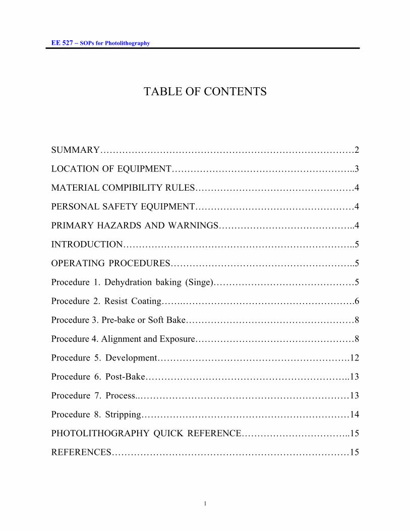
SUMMARY EQUIPMENT
1. Photolithography Bench 2. Photoresist Spin Coater (Specialty Coating Systems Model P6700)
3. Oriel 3 Timer Integrator 4. 68810 Arc lamp power supply
5. Vacuum Control Box 6. Oriel 3 Aligner
Vacuum Control
Main Vacuum
Vacuum Leak
Timer:8s
Split-field Microscopes
chuck
EE 527 – SOPs for Photolithography
3
7. Digital Hot Plate (Dataplate-720) 8. Inspection Microscope
MATERIALS 1. AZ 1512 POSITIVE PHOTORESIST
2. AZ 300 MIF DEVELOPER
3. 3 inch wafer matching the glass plate on the hot plate
4. IPA and DI-water to clean and dry the wafer
5. Acetone for stripping the photoresist
6. BOE for wet etching
CONTACT
Prof.: BOBERT BRUCE DARLING
Email: [email protected]
Phone: (206) 543-4707 Office: 226 EEB
Department of Electrical Engineering, University of Washington
LOCATION OF EQUIPMENT
The Photolithography Bench, Photoresist Spin Coater (Specialty Coating Systems Model
P6700 – “SCS”), Oriel 3” Aligner, and Hot Plate are located in the room B025B of the EE
MicroFabrication Laboratory in the Electrical Engineering building at the University of
Washington. The SCS photoresist spin-coater and spinner are located on the photolithography
bench. The hot plate is located at the table next to the photolithography bench. The Oriel 3”
aligner is on the table that is opposite to the hot plate.
ON/OFF
Plate Temp.
ENT
Glass Plate
EE 527 – SOPs for Photolithography
4
MATERIAL COMPABILITIES RULES
The spin-coater accepts only positive photoresist and up to 4” inch wafer. The Oriel 3” aligner
allows up to 3" wafer and 1mm wafer thickness. The hot plate accepts wafers of any sizes that
fit within the glass plate, which is placed on top of the hot plate surface.
PERSONAL SAFETY EQUIPMENT
Personal protective equipment is not needed for the routine operation of this instrument, but
when using HF for etching purposes as one possible process Trionic gloves, facemask and
apron are required. Powder free latex or PVC gloves are required for handling the sample
holders and internal parts of the equipment to keep finger print oils off of the internal surfaces.
PRIMARY HAZARDS AND WARNINGS
The primary hazards associated with photolithography are the chemicals. In general, regular
chemical handling measures should be adopted. Details on chemical storage, handling and
disposal are described in the Solid State Laboratory Handbook. Make sure not to store or
combine any two of the following chemical types: acid/bases, flammable solvents and
oxidizers. These type of chemicals should be separate form each other because they could
produce a potentially explosive situation.
Positive photoresist materials are carcinogen and blood poison, keep it under fume hood when
spinning and see “precautions” section in the spin-coating procedure for more details.
The Hg arc lamp is used as a source of ultraviolet radiation during exposure. Ultraviolet
radiation can cause burns of the skin or of the outer layers of the eye. Chronic exposure to
ultraviolet radiation can cause skin cancer. The ultraviolet illumination system has been
designed so that the user is not exposed to the UV. However, the user should avoid looking
directly at the UV source and avoid exposure to reflected or diffused UV from the lamp. In
addition, the Hg arc lamp operates at high voltage and the user should make sure that both the
power supply and the illuminator are covered properly, and the cables are properly connected.
Incorrect cable connections can cause explosion and human injuries.
EE 527 – SOPs for Photolithography
5
INTRODUCTION
Photolithography, also called Optical lithography, is a process used in micro fabrication to
selectively remove parts of a thin film or the bulk of a substrate. To do this, it uses light to
transfer a geometric pattern from a photo mask to a light-sensitive chemical photo resist, or
simply "resist" on the substrate. AZ 1512 is a positive photoresist1 which could response to the
whole UV-spectrum from 310nm — 440nm covering the three main mercury lines, i, h and g.
AZ 1512 resist is compatible with all common developers used for positive photoresists, like
AZ 300 MIF. Development time at 20-30 seconds can result in a high throughput lithographic
process. The goal of this standard operating procedure (SOP) is to update the previous SOP
for AZ 1512 photoresist Photolithography written in 1999. This AZ 1512 resist
Photolithography SOP mainly focuses on the processes: Alignment, Exposure and
Development. Each procedure also includes safety and precaution issues. Troubleshooting is
addressed as well. The next sections will describe the SOP procedures for AZ 1512
photolithography.
OPERATIONAL PROCEDURES AND PRECAUTIONS Procedure 1: Dehydration baking (Singe)
This is a step for surface preparation. Ideally, the wafer surface should be clean and particle
free which can be realized via a convection oven or hot plate at a certain condition which is
described below. In this MicroFabrication lab, a hot plate is used to drive off water vapor
from the wafer surface, which is shown in Equipment 7.
Steps to follow:
1. Turn on the hot plate
2. Adjust the desired temperature by pressing the ENT, plate temperature buttons, type
the desired temperature and press ENT once again. The dehydration baking
temperature is set at 90 ºC. The hot plate takes about 8~10 minutes to reach this
temperature. Wait until the temperature has been stabilized.
3. Place the glass plate on the hot plate to provide a smooth surface, desired thermal
contact and heating uniformity to the wafer.
4. Before placing the wafer on the glass plate, set a timer for 60 sec.
5. Place the wafer face up on the glass plate in a way that it is completely centered to
conduct heat evenly.

EE 527 – SOPs for Photolithography
6
6. Start the timer for 60 sec and remove the wafer from the glass plate after the timer has
ended.
Precautions:
After turning on the hot plate do not have direct contact with the glass plate or the aluminum
foil covering the hot plate surface. These surfaces are at high temperature that can cause skin-
burned.
Procedure 2: Resist Coating
This process is to apply uniform, adherent and defect-free resist film with a desired thickness
over the wafer. Usually it is conducted by using a spin-coater which rapidly spins the wafer.
The final spin speed is around 2000-5000 RPM, which depends on the desired film thickness of
a certain photoresist. Figure 1 shows the relation between spin-speed (RPM) and film thickness
(m) for AZ 1500 photoresists1. The positive photoresist used in the MicroFabrication
Laboratory is AZ 1512. The spin-coater is located in the right hand side of the
photolithography bench, see Equipment 1 and 2. An initial set-up is needed before conducting
the spin-coating.
Fig. 1 Spin Speed Curve for AZ 1500 Photoresist Products
Initial set-up:
1. On the photolithography bench, turn on the air and vacuum supplies by turning the
control knobs on the right panel with one complete 360 degree turn CCW for the
vacuum and a little bit for the air knob.
EE 527 – SOPs for Photolithography
7
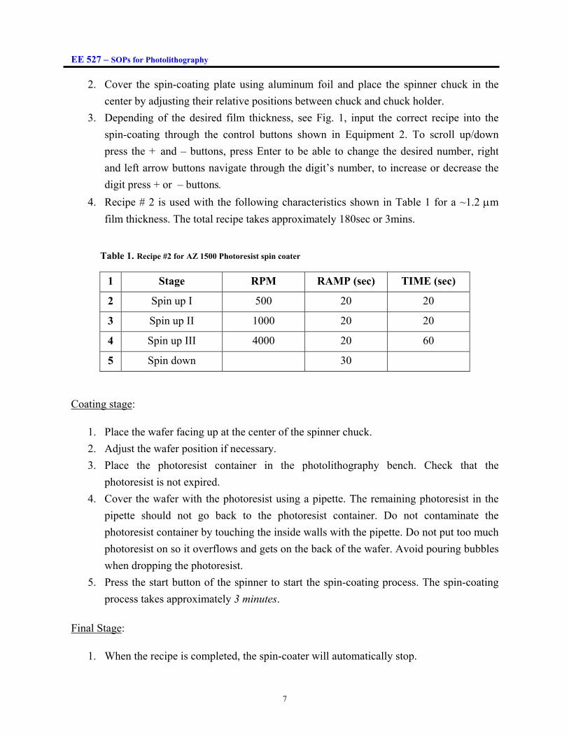
2. Cover the spin-coating plate using aluminum foil and place the spinner chuck in the
center by adjusting their relative positions between chuck and chuck holder.
3. Depending of the desired film thickness, see Fig. 1, input the correct recipe into the
spin-coating through the control buttons shown in Equipment 2. To scroll up/down
press the + and – buttons, press Enter to be able to change the desired number, right
and left arrow buttons navigate through the digit’s number, to increase or decrease the
digit press + or – buttons.
4. Recipe # 2 is used with the following characteristics shown in Table 1 for a ~1.2 m
film thickness. The total recipe takes approximately 180sec or 3mins.
Table 1. Recipe #2 for AZ 1500 Photoresist spin coater
1 Stage RPM RAMP (sec) TIME (sec)
2 Spin up I 500 20 20
3 Spin up II 1000 20 20
4 Spin up III 4000 20 60
5 Spin down 30
Coating stage:
1. Place the wafer facing up at the center of the spinner chuck.
2. Adjust the wafer position if necessary.
3. Place the photoresist container in the photolithography bench. Check that the
photoresist is not expired.
4. Cover the wafer with the photoresist using a pipette. The remaining photoresist in the
pipette should not go back to the photoresist container. Do not contaminate the
photoresist container by touching the inside walls with the pipette. Do not put too much
photoresist on so it overflows and gets on the back of the wafer. Avoid pouring bubbles
when dropping the photoresist.
5. Press the start button of the spinner to start the spin-coating process. The spin-coating
process takes approximately 3 minutes.
Final Stage:
1. When the recipe is completed, the spin-coater will automatically stop.
EE 527 – SOPs for Photolithography
8
2. Remove the wafer from the spinner chuck and check the pattern is uniformly coated. If
the pattern does not look uniform, remove or strip off the photoresist by using acetone
and see procedure 9 for more details, and repeat the resist coating process.
3. If the pattern looks uniform, clean the back-side of the wafer by using a dust-free wiper
with acetone to remove any photoresist on the backside.
Precautions:
a) Try to not have direct contact with the photoresist. The coating solvent of the positive
photoresist materials is carcinogen and blood poison.
b) Use a fume hood during the spinning process because 99.9% of the positive photoresist
solvent is removed during this process.
c) Pipettes and bottles containing wet photoresist should be collected and marked as
hazardous waste. Dry photoresist such as the one found in the spinner bowl or dust-free
wipers should go into the regular trash.
Procedure 3. Pre-bake or Soft Bake
The soft bake removes the solvent from the photoresist; improve the adhesion of the resist to
the wafer, densify the photoresist and it is usually set at 90º-100ºC using a hot plate for 1
minute. For thicker films, a longer bake is required. This procedure is similar to procedure 1.
Procedure 4: Alignment and Exposure
The purpose of procedure 5 is to polymerize selected areas of photo-resist coated substrate by
precise – repeatable aligning of a mask to a pattern, thereby exposing the selected part of photo
resist-substrate to ultraviolet light through the mask. This step is a key procedure in order to
successfully transferring the desired patterns onto the wafer. The whole systems mainly
contain: UV-light source, UV-light power supply,2 Vacuum control box and Oriel 3-in Aligher.
Steps to follow:
1. Turn on the POWER switch on the front intensity controller of the UV-light power supply
shown in the Equipment 4 to the ON position.
2. Press START to produce ignition of the mercury arc lamp and wait until the source is
stabilized.
3. Mask alignment: this is a step for transferring the pattern from a mask to photoresist

EE 527 – SOPs for Photolithography
9
through UV exposure involved spit-field technique; in the MicroFabrication lab, the source
of UV light is a mercury arc lamp with center wavelengths covering 365nm (i-line) and
437nm (g-line) and exposure power from 200 Watts to 500 Watts which can be adjusted by
68810 Arc Lamp Power supply 1 shown in Equipment 4. The exposure dose and time of
UV light depend on which type of photoresist is chosen, the type of the mask and the
thickness coated on the wafer. Specific to our experiment, exposure power of 300 Watts
was chosen for 8 seconds exposure time in order to coat 1um thickness of AZ 1512 positive
photoresist. As shown in Figure 2, Oriel 83210-V mask alignment fixture3 and Vacuum
control box (shown in Equipment 5) are used to load mask and align the wafer to the
photomask. This is a CONTACT aligner which can minimize the diffraction at the edges of
mask features. There are three degrees of freedom between wafer and mask (x, y, )
translation controllers to achieve the alignment. For application of split-field technique,
refer to the SOP for Split Field Microscope. In detail, the procedure for mask alignment can
be followed:
Fig. 2 Oriel 83210-V mask alignment fixture
a) Loading of Photomask: Raise the photomask holder by switching to mask frame to
"raise" position. Then place the photomask, ensuring the brown (chrome coating) side
is facing down and is centered in the holder, so that there is enough room to rotate in
the assembly. The photomask should be held at rest by the screws. Then carefully
lower the mask assembly holder by switching the mask frame to the "lower" position
to hold both photo mask and holder together as one unit.
b) Loading of Wafer: after pre-baking, center the wafer with the photoresist side facing
up to photo mask on the center of wafer holder. Align the flat of the wafer as parallel
EE 527 – SOPs for Photolithography
10
as possible to the vacuum chuck. After loading the wafer onto the chuck, put the
photomask holder back down and open vacuum control knob until the pressure goes to
27mmHg. This is to vacuum hold the wafer to the chuck. Now raise the wafer close to
the mask via Z-axis of the height adjustment until a small shadow appears between the
mask and wafer. A small gap is set between the wafer and the photomask to examine
the mask patterns alignment. This performs a Non-Contact setup.
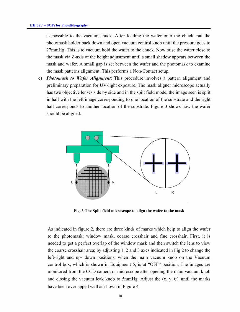
c) Photomask to Wafer Alignment: This procedure involves a pattern alignment and
preliminary preparation for UV-light exposure. The mask aligner microscope actually
has two objective lenses side by side and in the spilt field mode, the image seen is split
in half with the left image corresponding to one location of the substrate and the right
half corresponds to another location of the substrate. Figure 3 shows how the wafer
should be aligned.
Fig. 3 The Split-field microscope to align the wafer to the mask
As indicated in figure 2, there are three kinds of marks which help to align the wafer
to the photomask: window mask, coarse crosshair and fine crosshair. First, it is
needed to get a perfect overlap of the window mask and then switch the lens to view
the coarse crosshair area; by adjusting 1, 2 and 3 axes indicated in Fig.2 to change the
left-right and up- down positions, when the main vacuum knob on the Vacuum
control box, which is shown in Equipment 5, is at “OFF” position. The images are
monitored from the CCD camera or microscope after opening the main vacuum knob
and closing the vacuum leak knob to 5mmHg. Adjust the (x, y, ) until the marks
have been overlapped well as shown in Figure 4.

EE 527 – SOPs for Photolithography
11
Fig. 4 Mask alignment features
4. Exposing the wafer to UV light: After finishing the alignment, push the alignment fixture
under the UV-light, adjust the desire time to expose from the “Oriel 3-in aligner-timer
integrator” and check the UV light power, then switch UV light to “EXPOSE”. During the
exposure, make sure you turn away from the UV light in order to protect yourself from the
UV exposure. In the MicroFabrication Lab, the exposure time is 8 seconds under 300
Watts UV dose exposes on a ~1.2 m thickness of AZ 1512 photoresist.
5. Taking out the wafer from the chuck: Make sure to switch the main vacuum knob on the
vacuum control box to the “OFF” position and lower wafer chuck. Switch the vacuum leak
“ON”, the vacuum control knob now should be closed.
Precautions:
a) Never make any adjustment when “MAIN VACUUM” is “ON”
b) Slowly close the vacuum leak knob until reaching no more than 5mmHg
c) Before releasing the wafer, turn off the main vacuum and lower wafer chuck
d) Try to align the wafer with the mask as precisely as possible; do so repeatedly if
necessary before exposing it to the UV light
e) During UV exposure, be sure not to look at the light
f) According to the {A, B, C} Dill parameters1 of AZ 1512 positive photoresist1, a sharp
boundary between bleached and unbleached regions depends on the choice of the
exposure wavelength. AZ 1512 positive photoresist can be well established g-line with
high resolution at UV light wavelength (=437 nm) based on the contact printing
equation: db 5.032 (here 2b is minimum pitch of line-space pattern and d is the

EE 527 – SOPs for Photolithography
12
resist thickness).
g) Choosing the proper exposure time is also very critical in photolithography which
depends on the exposure dose, thickness of the photoresist and f-number of objection
lens in UV light.
Therefore, any misalignment and wrong choice of UV light parameters will result in messing up the pattern transfer.
Procedure 5: Development
Development is a process to remove the unexposed areas of an AZ 1512 resist film and leave
the correct pattern on the wafer. In addition, the developer will remove the exposed positive
photoresist. The unexposed photoresist will remain covering the desired areas to protect them
from chemicals used in following steps as etching or lift-off processes. The developer in this
case is AZ 300MIF.
Steps to follow:
1. Immerse the wafer in the developer (AZ 300 MIF) for 30-35 seconds for approximately
~1.2 m photoresist thickness at 231 ºC.
2. Mild AGITATION of the wafer is required to ensure uniform development during the
immersion time.
3. Immerse the wafer into DI water rinse for 20 seconds with AGITATION.
4. Spin dry: place the wafer on the spinner chuck covering the wafer with DI water for 20
seconds at 3000 RPM.
5. Inspect resist pattern under microscope for proper development. Under the microscope
the pink color of the photoresist should have disappeared from the exposed areas.
Precautions:
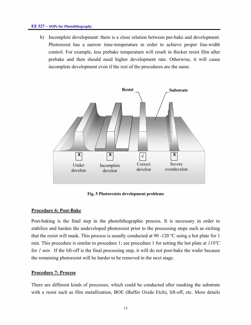
There are usually three kinds of issues which should be take care during the development:
under development, incomplete development, and over development as shown in Figure 5.
a) Underdevelopment or overdevelopment: a feature appears to be greatly smaller or
bigger than the desired size. This is caused by underdevelopment or overdevelopment.
Many factors could introduce underdevelopment such as prebake temperature and
time, exposure dose, and development time. The detailed troubleshooting techniques
have already been addressed in the previous SOP for photolithography in order to
avoid underdevelopment or overdevelopment (see Procedure 7: inspection)
EE 527 – SOPs for Photolithography
13
XX X
Under develop
Incomplete develop
Correctdevelop
Severe overdevelop
Resist Substrate
b) Incomplete development: there is a close relation between pre-bake and development.
Photoresist has a narrow time-temperature in order to achieve proper line-width
control. For example, less prebake temperature will result in thicker resist film after
prebake and then should need higher development rate. Otherwise, it will cause
incomplete development even if the rest of the procedures are the same.
Fig. 5 Photoresists development problems
Procedure 6: Post-Bake
Post-baking is the final step in the photolithographic process. It is necessary in order to
stabilize and harden the undeveloped photoresist prior to the processing steps such as etching
that the resist will mask. This process is usually conducted at 90 -120 ºC using a hot plate for 1
min. This procedure is similar to procedure 1; see procedure 1 for setting the hot plate at 110ºC
for 1 min. If the lift-off is the final processing step, it will do not post-bake the wafer because
the remaining photoresist will be harder to be removed in the next stage.
Procedure 7: Process
There are different kinds of processes, which could be conducted after masking the substrate
with a resist such as film metallization, BOE (Buffer Oxide Etch), lift-off, etc. More details
EE 527 – SOPs for Photolithography
14
could be found in the respective SOPs, but a general description of each process is explained in
the following table:
Characteristics I Characteristics II
Film metallization Evaporating Cr/Al/Cr layers by using the resistance vacuum system
Cr layer: 100 Angstroms Al layer: 800 Angstroms Cr layer: 100 Angstroms
Lift-off metal Immerse in acetone with ultrasonic agitation until removing completely the photoresist with the metal layer on top of it.
Immerse in IPA for removing acetone and dry using the spin-coater with DI water for 20sec. at 3000 RPM
BOE Immerse in BOE with gently shaking for 25 min. and after for 2 min. in DI water
Dry using the spin-coater with DI water for 20sec at 3000 RPM
Precautions:
a) Use the Trionic gloves when dealing with BOE, which has small molecules that easily
penetrate through skin and regular plastic gloves.
b) BOE contains HF (Hydrofluoric acid) usually 10:1 ratio by volume of HF: NH4F
c) HF vapor produces edema of the lungs and can damage the cornea. HF is extremely
dangerous to skin contact; it produces very severe painful burns. There is no remedy
for HF burns.
Procedure 8: Stripping
The final process consists in completely removing the photoresist after the specific process
explained in procedure 8 is done. The stripping is necessary if the sacrificial photoresist layer
remains after the processing step. Typically acetone is used as a solvent to swell the photoresist
and remove it from the wafer.
Steps to follow:
1. Pour some acetone in a beaker where the wafer could completely fit.
2. Immerse the wafer and agitate it in the acetone beaker for 35 seconds.
3. Remove the acetone on the wafer by placing the wafer on the spin-coater for 20seconds
at 3000 RPM with IPA.
4. Dry the wafer with DI water using the spin-coater for 20seconds at 3000 RPM.
EE 527 – SOPs for Photolithography
15
5. Examine under the microscope to ensure that there is not photoresist remaining. If there
is photoresist, repeat steps 2 to 5.
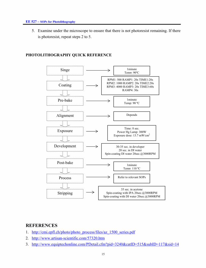
PHOTOLITHOGRAPHY QUICK REFERENCE
REFERENCES 1. http://cmi.epfl.ch/photo/photo_process/files/az_1500_series.pdf
2. http://www.artisan-scientific.com/57320.htm
3. http://www.equiptechonline.com/PDetail.cfm?pid=3240&catID=515&subID=117&sid=14
Singe
Coating
Pre-bake
Alignment
Exposure
Development
Post-bake
Process
Stripping
1minute Temp: 90ºC
RPM1: 500 RAMP1: 20s TIME1:20s RPM2: 1000 RAMP2: 20s TIME2:20s RPM3: 4000 RAMP3: 20s TIME3:60s
RAMP4: 30s
1minute Temp: 90 ºC
Depends
Time: 8 sec. Power Hg Lamp: 300W
Exposure dose: 13.7 mW/cm2
30-35 sec. in developer 20 sec. in DI water
Spin-coating DI water 20sec.@3000RPM
1minute Temp: 110 ºC
Refer to relevant SOPs
35 sec. in acetone Spin-coating with IPA 20sec.@3000RPM
Spin-coating with DI water 20sec.@3000RPM