Automotive door actuator driver - STMicroelectronics · Automotive door actuator driver Datasheet...
68
This is information on a product in full production. December 2016 DocID18260 Rev 6 1/68 L99DZ80EP Automotive door actuator driver Datasheet - production data Features AEC-Q100 qualified One full bridge for 6 A load (R ON = 150 m) Two half bridges for 3 A load (R ON = 300 m) Two half bridges for 0.5 A load (R ON = 1600 m) One high-side driver for 5 A load (R ON = 100 m) One configurable high-side driver for up to 1.5 A (R ON = 500 m) or 0.35 A (R ON = 1600 m) load One configurable high-side driver for 0.7 A (R ON = 800 m) or 0.35 A (R ON = 1600 m) load Two high-side drivers for 0.5 A load (R ON = 1600 m) Programmable softstart function to drive loads with higher inrush currents as current limitation value Very low V S current consumption in standby mode (I S < 6 μA typ; T j 85 °C) Current monitor output for all high-side drivers Central two-stage charge pump Motor bridge driver with full R dson down to 6 V Device contains temperature warning and protection Open-load detection for all outputs Overcurrent protection for all outputs Separated half bridges for door lock motor Programmable PWM control of all outputs STM standard serial peripheral interface (ST- SPI 3.1) Control block for electrochromic element Electrochromic element can be negatively discharged Prepared for additional fail-safe path for H-bridge Applications Door actuator driver with 6 bridges for double door lock control, mirror fold and mirror axis control, high-side driver for mirror defroster, bulbs and LEDs. Control block with external MOS transistor for charging / discharging of electrochromic glass. Motor bridge driver. H-bridge control for external power transistors Description The L99DZ80EP is a microcontroller driven multifunctional door actuator driver for automotive applications. Up to five DC motors and five grounded resistive loads can be driven with six half bridges and five high-side drivers. Four external MOS transistors in bridge configuration can be driven. An electrochromic mirror glass can be controlled using the integrated SPI-driven module in conjunction with an external MOS transistor. The mirror glass can also be discharged through a negative supply. The integrated SPI controls all operating modes (forward, reverse, brake and high impedance). All diagnostic information is available via SPI read. Table 1. Device summary Package Order codes Tray Tape and reel TQFP-64 L99DZ80EP L99DZ80EPTR www.st.com
Transcript of Automotive door actuator driver - STMicroelectronics · Automotive door actuator driver Datasheet...

This is information on a product in full production.
December 2016 DocID18260 Rev 6 1/68
L99DZ80EP
Automotive door actuator driver
Datasheet - production data
Features
AEC-Q100 qualified
One full bridge for 6 A load (RON = 150 m)
Two half bridges for 3 A load (RON = 300 m)
Two half bridges for 0.5 A load(RON = 1600 m)
One high-side driver for 5 A load(RON = 100 m)
One configurable high-side driver for up to1.5 A (RON = 500 m) or 0.35 A(RON = 1600 m) load
One configurable high-side driver for 0.7 A(RON = 800 m) or 0.35 A (RON = 1600 m)load
Two high-side drivers for 0.5 A load(RON = 1600 m)
Programmable softstart function to drive loadswith higher inrush currents as current limitationvalue
Very low VS current consumption in standbymode (IS < 6 µA typ; Tj 85 °C)
Current monitor output for all high-side drivers
Central two-stage charge pump
Motor bridge driver with full Rdson down to 6 V
Device contains temperature warning andprotection
Open-load detection for all outputs
Overcurrent protection for all outputs
Separated half bridges for door lock motor
Programmable PWM control of all outputs
STM standard serial peripheral interface (ST-SPI 3.1)
Control block for electrochromic element
Electrochromic element can be negativelydischarged
Prepared for additional fail-safe path forH-bridge
Applications
Door actuator driver with 6 bridges for doubledoor lock control, mirror fold and mirror axiscontrol, high-side driver for mirror defroster,bulbs and LEDs.
Control block with external MOS transistor forcharging / discharging of electrochromic glass.Motor bridge driver.
H-bridge control for external power transistors
Description
The L99DZ80EP is a microcontroller driven multifunctional door actuator driver for automotive applications. Up to five DC motors and five grounded resistive loads can be driven with six half bridges and five high-side drivers. Four external MOS transistors in bridge configuration can be driven. An electrochromic mirror glass can be controlled using the integrated SPI-driven module in conjunction with an external MOS transistor. The mirror glass can also be discharged through a negative supply. The integrated SPI controls all operating modes (forward, reverse, brake and high impedance). All diagnostic information is available via SPI read.
Table 1. Device summary
PackageOrder codes
Tray Tape and reel
TQFP-64 L99DZ80EP L99DZ80EPTR
www.st.com

Contents L99DZ80EP
2/68 DocID18260 Rev 6
Contents
1 Block diagram and pin description . . . . . . . . . . . . . . . . . . . . . . . . . . . . . 7
2 Electrical specifications . . . . . . . . . . . . . . . . . . . . . . . . . . . . . . . . . . . . . 11
2.1 Absolute maximum ratings . . . . . . . . . . . . . . . . . . . . . . . . . . . . . . . . . . . . .11
2.2 ESD protection . . . . . . . . . . . . . . . . . . . . . . . . . . . . . . . . . . . . . . . . . . . . . 12
2.3 Thermal data . . . . . . . . . . . . . . . . . . . . . . . . . . . . . . . . . . . . . . . . . . . . . . 12
2.4 Package and PCB thermal data . . . . . . . . . . . . . . . . . . . . . . . . . . . . . . . . 13
2.4.1 TQFP-64 thermal data . . . . . . . . . . . . . . . . . . . . . . . . . . . . . . . . . . . . . . 13
2.5 Electrical characteristics . . . . . . . . . . . . . . . . . . . . . . . . . . . . . . . . . . . . . . 15
2.6 Outputs OUT1 - OUT11, ECV, ECFD . . . . . . . . . . . . . . . . . . . . . . . . . . . . 17
2.7 H-bridge driver . . . . . . . . . . . . . . . . . . . . . . . . . . . . . . . . . . . . . . . . . . . . . 21
2.8 Electrochrome mirror driver . . . . . . . . . . . . . . . . . . . . . . . . . . . . . . . . . . . 25
2.9 SPI / logic – electrical characteristics . . . . . . . . . . . . . . . . . . . . . . . . . . . . 27
3 Application information . . . . . . . . . . . . . . . . . . . . . . . . . . . . . . . . . . . . . 32
3.1 Dual power supply: VS and VCC . . . . . . . . . . . . . . . . . . . . . . . . . . . . . . . 32
3.2 Wake up and Active mode/standby mode . . . . . . . . . . . . . . . . . . . . . . . . 32
3.3 Charge pump . . . . . . . . . . . . . . . . . . . . . . . . . . . . . . . . . . . . . . . . . . . . . . 32
3.4 Diagnostic functions . . . . . . . . . . . . . . . . . . . . . . . . . . . . . . . . . . . . . . . . . 32
3.5 Overvoltage and undervoltage detection at VS . . . . . . . . . . . . . . . . . . . . 33
3.6 Overvoltage and undervoltage detection at VCC . . . . . . . . . . . . . . . . . . . 33
3.7 Temperature warning and shutdown . . . . . . . . . . . . . . . . . . . . . . . . . . . . 33
3.8 Inductive loads . . . . . . . . . . . . . . . . . . . . . . . . . . . . . . . . . . . . . . . . . . . . . 34
3.9 Open-load detection . . . . . . . . . . . . . . . . . . . . . . . . . . . . . . . . . . . . . . . . . 34
3.10 Overcurrent detection . . . . . . . . . . . . . . . . . . . . . . . . . . . . . . . . . . . . . . . . 34
3.11 Current monitor . . . . . . . . . . . . . . . . . . . . . . . . . . . . . . . . . . . . . . . . . . . . 34
3.12 PWM mode of the power outputs . . . . . . . . . . . . . . . . . . . . . . . . . . . . . . . 34
3.13 Cross-current protection . . . . . . . . . . . . . . . . . . . . . . . . . . . . . . . . . . . . . . 35
3.14 Programmable soft-start function to drive loads with higher inrush current . 35
3.15 H-bridge control (DIR, PWMH, bits SD, SDS) . . . . . . . . . . . . . . . . . . . . . 36
3.16 H-bridge driver slew-rate control . . . . . . . . . . . . . . . . . . . . . . . . . . . . . . . 37

DocID18260 Rev 6 3/68
L99DZ80EP Contents
4
3.17 Resistive low . . . . . . . . . . . . . . . . . . . . . . . . . . . . . . . . . . . . . . . . . . . . . . 38
3.18 Short circuit detection/drain source monitoring . . . . . . . . . . . . . . . . . . . . 38
3.19 H-bridge monitoring in off-mode . . . . . . . . . . . . . . . . . . . . . . . . . . . . . . . . 39
3.20 Programmable cross current protection . . . . . . . . . . . . . . . . . . . . . . . . . . 41
3.21 Controller of electrochromic glass . . . . . . . . . . . . . . . . . . . . . . . . . . . . . . 42
3.22 Watchdog . . . . . . . . . . . . . . . . . . . . . . . . . . . . . . . . . . . . . . . . . . . . . . . . . 44
4 Functional description of the SPI . . . . . . . . . . . . . . . . . . . . . . . . . . . . . 45
4.1 General description . . . . . . . . . . . . . . . . . . . . . . . . . . . . . . . . . . . . . . . . . 45
4.1.1 Chip Select Not (CSN) . . . . . . . . . . . . . . . . . . . . . . . . . . . . . . . . . . . . . . 45
4.1.2 Serial Data In (DI) . . . . . . . . . . . . . . . . . . . . . . . . . . . . . . . . . . . . . . . . . 45
4.1.3 Serial Clock (CLK) . . . . . . . . . . . . . . . . . . . . . . . . . . . . . . . . . . . . . . . . . 45
4.1.4 Serial Data Out (DO) . . . . . . . . . . . . . . . . . . . . . . . . . . . . . . . . . . . . . . . 45
4.1.5 SPI communication flow . . . . . . . . . . . . . . . . . . . . . . . . . . . . . . . . . . . . 45
4.2 Command byte . . . . . . . . . . . . . . . . . . . . . . . . . . . . . . . . . . . . . . . . . . . . . 47
4.2.1 Operation code definition . . . . . . . . . . . . . . . . . . . . . . . . . . . . . . . . . . . . 47
4.3 Device memory map . . . . . . . . . . . . . . . . . . . . . . . . . . . . . . . . . . . . . . . . 47
5 SPI - control and status registers . . . . . . . . . . . . . . . . . . . . . . . . . . . . . 49
5.1 Control Register 0 . . . . . . . . . . . . . . . . . . . . . . . . . . . . . . . . . . . . . . . . . . 50
5.2 Control Register 1 . . . . . . . . . . . . . . . . . . . . . . . . . . . . . . . . . . . . . . . . . . 50
5.3 Control Register 2 . . . . . . . . . . . . . . . . . . . . . . . . . . . . . . . . . . . . . . . . . . 51
5.4 Control Register 3 . . . . . . . . . . . . . . . . . . . . . . . . . . . . . . . . . . . . . . . . . . 52
5.5 Control Register 4 . . . . . . . . . . . . . . . . . . . . . . . . . . . . . . . . . . . . . . . . . . 53
5.6 Control Register 5 . . . . . . . . . . . . . . . . . . . . . . . . . . . . . . . . . . . . . . . . . . 53
5.7 Control Register 6 . . . . . . . . . . . . . . . . . . . . . . . . . . . . . . . . . . . . . . . . . . 54
5.8 Configuration Register . . . . . . . . . . . . . . . . . . . . . . . . . . . . . . . . . . . . . . . 55
5.9 Status Register 0 . . . . . . . . . . . . . . . . . . . . . . . . . . . . . . . . . . . . . . . . . . . 55
5.10 Status Register 1 . . . . . . . . . . . . . . . . . . . . . . . . . . . . . . . . . . . . . . . . . . . 56
5.11 Status Register 2 . . . . . . . . . . . . . . . . . . . . . . . . . . . . . . . . . . . . . . . . . . . 57
5.12 Status Register 3 . . . . . . . . . . . . . . . . . . . . . . . . . . . . . . . . . . . . . . . . . . . 57
6 Package and packing information . . . . . . . . . . . . . . . . . . . . . . . . . . . . . 59
6.1 ECOPACK® package . . . . . . . . . . . . . . . . . . . . . . . . . . . . . . . . . . . . . . . . 59
6.2 TQFP-64 mechanical data . . . . . . . . . . . . . . . . . . . . . . . . . . . . . . . . . . . . 59

Contents L99DZ80EP
4/68 DocID18260 Rev 6
6.3 TQFP-64 packing information . . . . . . . . . . . . . . . . . . . . . . . . . . . . . . . . . 61
7 Revision history . . . . . . . . . . . . . . . . . . . . . . . . . . . . . . . . . . . . . . . . . . . 65

DocID18260 Rev 6 5/68
L99DZ80EP List of tables
5
List of tables
Table 1. Device summary . . . . . . . . . . . . . . . . . . . . . . . . . . . . . . . . . . . . . . . . . . . . . . . . . . . . . . . . . . 1Table 2. Pin definitions and functions . . . . . . . . . . . . . . . . . . . . . . . . . . . . . . . . . . . . . . . . . . . . . . . . . 8Table 3. Absolute maximum ratings . . . . . . . . . . . . . . . . . . . . . . . . . . . . . . . . . . . . . . . . . . . . . . . . . 11Table 4. ESD protection . . . . . . . . . . . . . . . . . . . . . . . . . . . . . . . . . . . . . . . . . . . . . . . . . . . . . . . . . . 12Table 5. Operating junction temperature . . . . . . . . . . . . . . . . . . . . . . . . . . . . . . . . . . . . . . . . . . . . . 12Table 6. Temperature warning and thermal shutdown . . . . . . . . . . . . . . . . . . . . . . . . . . . . . . . . . . . 12Table 7. Package thermal impedance . . . . . . . . . . . . . . . . . . . . . . . . . . . . . . . . . . . . . . . . . . . . . . . 12Table 8. Supply . . . . . . . . . . . . . . . . . . . . . . . . . . . . . . . . . . . . . . . . . . . . . . . . . . . . . . . . . . . . . . . . . 15Table 9. Overvoltage and undervoltage detection . . . . . . . . . . . . . . . . . . . . . . . . . . . . . . . . . . . . . . 15Table 10. Current monitor output (CM). . . . . . . . . . . . . . . . . . . . . . . . . . . . . . . . . . . . . . . . . . . . . . . . 16Table 11. Charge pump . . . . . . . . . . . . . . . . . . . . . . . . . . . . . . . . . . . . . . . . . . . . . . . . . . . . . . . . . . . 16Table 12. On-resistance . . . . . . . . . . . . . . . . . . . . . . . . . . . . . . . . . . . . . . . . . . . . . . . . . . . . . . . . . . . 17Table 13. Power outputs switching times . . . . . . . . . . . . . . . . . . . . . . . . . . . . . . . . . . . . . . . . . . . . . . 19Table 14. Current monitoring . . . . . . . . . . . . . . . . . . . . . . . . . . . . . . . . . . . . . . . . . . . . . . . . . . . . . . . 19Table 15. Gate drivers for the external Power-MOS (H-bridge) . . . . . . . . . . . . . . . . . . . . . . . . . . . . . 21Table 16. Gate drivers for the external Power-MOS switching times . . . . . . . . . . . . . . . . . . . . . . . . . 21Table 17. Drain source monitoring . . . . . . . . . . . . . . . . . . . . . . . . . . . . . . . . . . . . . . . . . . . . . . . . . . . 24Table 18. Open-load monitoring . . . . . . . . . . . . . . . . . . . . . . . . . . . . . . . . . . . . . . . . . . . . . . . . . . . . . 25Table 19. Electrochrome mirror driver . . . . . . . . . . . . . . . . . . . . . . . . . . . . . . . . . . . . . . . . . . . . . . . . 25Table 20. Delay time from Standby to Active mode . . . . . . . . . . . . . . . . . . . . . . . . . . . . . . . . . . . . . . 27Table 21. Inputs: DI, CSN, CLK, DIR and PWMH . . . . . . . . . . . . . . . . . . . . . . . . . . . . . . . . . . . . . . . 27Table 22. AC-Characteristics . . . . . . . . . . . . . . . . . . . . . . . . . . . . . . . . . . . . . . . . . . . . . . . . . . . . . . . 28Table 23. Dynamic characteristics . . . . . . . . . . . . . . . . . . . . . . . . . . . . . . . . . . . . . . . . . . . . . . . . . . . 28Table 24. Watchdog . . . . . . . . . . . . . . . . . . . . . . . . . . . . . . . . . . . . . . . . . . . . . . . . . . . . . . . . . . . . . . 31Table 25. H-bridge control truth table . . . . . . . . . . . . . . . . . . . . . . . . . . . . . . . . . . . . . . . . . . . . . . . . . 36Table 26. H-bridge DS-monitor threshold . . . . . . . . . . . . . . . . . . . . . . . . . . . . . . . . . . . . . . . . . . . . . . 39Table 27. Cross-current protection time . . . . . . . . . . . . . . . . . . . . . . . . . . . . . . . . . . . . . . . . . . . . . . . 42Table 28. Command byte . . . . . . . . . . . . . . . . . . . . . . . . . . . . . . . . . . . . . . . . . . . . . . . . . . . . . . . . . . 47Table 29. Operation code definition . . . . . . . . . . . . . . . . . . . . . . . . . . . . . . . . . . . . . . . . . . . . . . . . . . 47Table 30. RAM memory map . . . . . . . . . . . . . . . . . . . . . . . . . . . . . . . . . . . . . . . . . . . . . . . . . . . . . . . 47Table 31. ROM memory map . . . . . . . . . . . . . . . . . . . . . . . . . . . . . . . . . . . . . . . . . . . . . . . . . . . . . . . 48Table 32. Global status byte . . . . . . . . . . . . . . . . . . . . . . . . . . . . . . . . . . . . . . . . . . . . . . . . . . . . . . . . 49Table 33. Control Register 0 . . . . . . . . . . . . . . . . . . . . . . . . . . . . . . . . . . . . . . . . . . . . . . . . . . . . . . . . 50Table 34. Control Register 1 . . . . . . . . . . . . . . . . . . . . . . . . . . . . . . . . . . . . . . . . . . . . . . . . . . . . . . . . 50Table 35. Control Register 2 . . . . . . . . . . . . . . . . . . . . . . . . . . . . . . . . . . . . . . . . . . . . . . . . . . . . . . . . 51Table 36. Control Register 3 . . . . . . . . . . . . . . . . . . . . . . . . . . . . . . . . . . . . . . . . . . . . . . . . . . . . . . . . 52Table 37. Control Register 4 . . . . . . . . . . . . . . . . . . . . . . . . . . . . . . . . . . . . . . . . . . . . . . . . . . . . . . . . 53Table 38. Control Register 5 . . . . . . . . . . . . . . . . . . . . . . . . . . . . . . . . . . . . . . . . . . . . . . . . . . . . . . . . 53Table 39. Control Register 6 . . . . . . . . . . . . . . . . . . . . . . . . . . . . . . . . . . . . . . . . . . . . . . . . . . . . . . . . 54Table 40. Configuration Register . . . . . . . . . . . . . . . . . . . . . . . . . . . . . . . . . . . . . . . . . . . . . . . . . . . . 55Table 41. Status Register 0 . . . . . . . . . . . . . . . . . . . . . . . . . . . . . . . . . . . . . . . . . . . . . . . . . . . . . . . . 55Table 42. Status Register 1 . . . . . . . . . . . . . . . . . . . . . . . . . . . . . . . . . . . . . . . . . . . . . . . . . . . . . . . . 56Table 43. Status Register 2 . . . . . . . . . . . . . . . . . . . . . . . . . . . . . . . . . . . . . . . . . . . . . . . . . . . . . . . . 57Table 44. Status Register 3 . . . . . . . . . . . . . . . . . . . . . . . . . . . . . . . . . . . . . . . . . . . . . . . . . . . . . . . . 57Table 45. TQFP-64 mechanical data . . . . . . . . . . . . . . . . . . . . . . . . . . . . . . . . . . . . . . . . . . . . . . . . . 59Table 46. Document revision history . . . . . . . . . . . . . . . . . . . . . . . . . . . . . . . . . . . . . . . . . . . . . . . . . 65

List of figures L99DZ80EP
6/68 DocID18260 Rev 6
List of figures
Figure 1. Block diagram . . . . . . . . . . . . . . . . . . . . . . . . . . . . . . . . . . . . . . . . . . . . . . . . . . . . . . . . . . . . 7Figure 2. Pin connection (top view) . . . . . . . . . . . . . . . . . . . . . . . . . . . . . . . . . . . . . . . . . . . . . . . . . . 10Figure 3. TQFP-64 2 layer PCB. . . . . . . . . . . . . . . . . . . . . . . . . . . . . . . . . . . . . . . . . . . . . . . . . . . . . 13Figure 4. TQFP-64 4 layer PCB. . . . . . . . . . . . . . . . . . . . . . . . . . . . . . . . . . . . . . . . . . . . . . . . . . . . . 13Figure 5. TQFP-64 thermal impedance junction to ambient vs PCB copper area . . . . . . . . . . . . . . . 14Figure 6. IGHxr ranges . . . . . . . . . . . . . . . . . . . . . . . . . . . . . . . . . . . . . . . . . . . . . . . . . . . . . . . . . . . 23Figure 7. IGHxf ranges. . . . . . . . . . . . . . . . . . . . . . . . . . . . . . . . . . . . . . . . . . . . . . . . . . . . . . . . . . . . 23Figure 8. H-driver delay times . . . . . . . . . . . . . . . . . . . . . . . . . . . . . . . . . . . . . . . . . . . . . . . . . . . . . . 24Figure 9. SPI timing parameters . . . . . . . . . . . . . . . . . . . . . . . . . . . . . . . . . . . . . . . . . . . . . . . . . . . . 29Figure 10. SPI input and output timing parameters . . . . . . . . . . . . . . . . . . . . . . . . . . . . . . . . . . . . . . . 30Figure 11. SPI delay description . . . . . . . . . . . . . . . . . . . . . . . . . . . . . . . . . . . . . . . . . . . . . . . . . . . . . 30Figure 12. Power-output (OUT<11:1>, ECV, ECFD) timing. . . . . . . . . . . . . . . . . . . . . . . . . . . . . . . . . 31Figure 13. Overcurrent recovery mode . . . . . . . . . . . . . . . . . . . . . . . . . . . . . . . . . . . . . . . . . . . . . . . . 36Figure 14. H-bridge GSHx slope . . . . . . . . . . . . . . . . . . . . . . . . . . . . . . . . . . . . . . . . . . . . . . . . . . . . . 38Figure 15. H-bridge diagnosis . . . . . . . . . . . . . . . . . . . . . . . . . . . . . . . . . . . . . . . . . . . . . . . . . . . . . . . 39Figure 16. H-bridge open-load detection (no open-load detected) . . . . . . . . . . . . . . . . . . . . . . . . . . . 40Figure 17. H-bridge open-load detection (open-load detected) . . . . . . . . . . . . . . . . . . . . . . . . . . . . . . 40Figure 18. H-bridge open-load detection (short to ground detected) . . . . . . . . . . . . . . . . . . . . . . . . . . 41Figure 19. H-bridge open-load detection with H-OLTH HIGH = ‘1’ (short to VS detected) . . . . . . . . . 41Figure 20. Electrochrome mirror driver with mirror referenced to ground . . . . . . . . . . . . . . . . . . . . . . 43Figure 21. Electrochrome mirror driver with mirror referenced to ECFD for negative discharge . . . . . 44Figure 22. Write and read SPI . . . . . . . . . . . . . . . . . . . . . . . . . . . . . . . . . . . . . . . . . . . . . . . . . . . . . . . 46Figure 23. TQFP-64 package dimension . . . . . . . . . . . . . . . . . . . . . . . . . . . . . . . . . . . . . . . . . . . . . . . 60Figure 24. TQFP-64 power lead-less tray shipment (no suffix) (part 1) . . . . . . . . . . . . . . . . . . . . . . . . 61Figure 25. TQFP-64 power lead-less tray shipment (no suffix) (part 2) . . . . . . . . . . . . . . . . . . . . . . . . 62Figure 26. TQFP-64 power lead-less tape and reel shipment (suffix “TR”) (part 1). . . . . . . . . . . . . . . 63Figure 27. TQFP-64 power lead-less tape and reel shipment (suffix “TR”) (part 2). . . . . . . . . . . . . . . 64

DocID18260 Rev 6 7/68
L99DZ80EP Block diagram and pin description
67
1 Block diagram and pin description
Figure 1. Block diagram

Block diagram and pin description L99DZ80EP
8/68 DocID18260 Rev 6
Table 2. Pin definitions and functions
Pin Symbol Function
57, 58 GND1Ground: reference potential. GND1 and GND2 are internally connected. GND1 supplies OUT1-3, GND2 supplies OUT4-6
Important: For the capability of driving the full current at the outputs, all pins of GND must be externally connected!
17, 18, 26, 31, 32
GND2
17 SGND Signal Ground: this pin is shared with GND2 pin
2, 3, 45, 46, 51, 52
VS1Power supply voltage for power stage outputs (external reverse protection required): for this input a ceramic capacitor as close as possible to GND is recommended. VS1 supplies OUT1-3, OUT7-11 and the internal VS supply, VS2 supplies OUT4-6
Important: For the capability of driving the full current at the outputs all pins of VS must be externally connected!
11, 12, 23, 36, 37
VS2
48, 49, 50 OUT11
High-side-driver output 11: the output is built by a high-side switch and is intended for resistive loads, hence the internal reverse diode from GND to the output is missing. For ESD reason a diode to GND is present but the energy which can be dissipated is limited. The High-side driver is a power DMOS transistor with an internal parasitic reverse diode from the output to VS (bulk-drain-diode). The output is overcurrent and open load protected.
Important: For the capability of driving the full current at the outputs all pins of OUT11 must be externally connected!
59, 60 OUT1
Half-bridge outputs 1,2,3,4,5,6: the output is built by a high side and a low side switch, which are internally connected. The output stage of both switches is a power DMOS transistor. Each driver has an internal parasitic reverse diode (bulk-drain-diode: high side driver from output to VS, low side driver from GND to output). This output is over current and open load protected.
56 OUT2
55 OUT3
19, 20, 21, 22
OUT4
27, 28, 29, 30
OUT5
24, 25 OUT6
40 DOSerial data output: the diagnosis data is available via the SPI and this 3-state-output. The output remains in 3-state, if the chip is not selected by the input CSN (CSN = high).
34 CMCurrent monitor output: depending on the selected multiplexer bits of the Control Register this output sources an image of the instant current through the corresponding high side driver with a fixed ratio.
35 CSNChip-Select-Not input: this input is low active and requires CMOS logic levels. The serial data transfer between the device and the micro controller is enabled by pulling the input CSN to low level.
41 DISerial data input: the input requires CMOS logic levels and receives serial data from the microcontroller. The data is a 24 bit control word and the most significant bit (MSB, bit 23) is transferred first.
38 CLKSerial clock input: this input controls the internal shift register of the SPI and requires CMOS logic levels.
33 DIR Direction Input: this input controls the H-Bridge Drivers

DocID18260 Rev 6 9/68
L99DZ80EP Block diagram and pin description
67
39 VCCSupply Voltage: 5 V supply. A ceramic capacitor as close as possible to GND is recommended.
44 OUT9
High-side-driver output 9: the output is built by a high side switch and is intended for resistive loads; hence the internal reverse diode from GND to the output is missing. For ESD reason a diode to GND is present but the energy which can be dissipated is limited. The high-side driver is a power DMOS transistor with an internal parasitic reverse diode from the output to VS (bulk-drain-diode). The output is over current and open load protected.
42 PWMHPWMH input: this input signal can be used to control the H-Bridge Gate drivers
43 ECDRECDR: using the device in EC control mode this pin is used to control the Gate of an external MOSFET.
62, 63 OUT7 High side driver output 8: see OUT9
Important: This output can be configured to supply a bulb with low on-resistance or a LED with higher on-resistance in a different application.61 OUT8
47 OUT10/ECHigh-side-driver-output 10: see OUT9
Important: Beside the OUT10-HS on/off bit this output can be switched on setting the ECON bit for electrochrome control mode with higher priority.
54 ECFD
ECFD: using the device in EC control mode this pin is used as “virtual GND” for the EC-glass. For EC-glasses, that require a negative discharge voltage, this supplies the fast discharge voltage. If no EC-glass is used, this pin must be connected to ground.
53 ECVECV: using the device in EC control mode this pin is used as voltage monitor input. For fast discharge an additional low-side-switch is implemented.
13 GH2 GH2: gate driver for power MOS high side switch in half-bridge 2
14 SH2 SH2: source of high-side switch in half-bridge 2
15 GL2 GL2: gate driver for power MOS low side switch in half-bridge 2
16 SL2 SL2: source of low side switch in half-bridge 2
64 GH1 GH1: gate driver for power MOS high side switch in half-bridge 1
1 SH1 SH1: source of high-side switch in half-bridge 1
4 GL1 GL1: gate driver for power MOS low side switch in half-bridge 1
5 SL1 SL1: source of low side switch in half-bridge 1
7 CP1P CP1P: charge pump pin for capacitor 1, positive side
8 CP1M CP1M: charge pump pin for capacitor 1, negative side
9 CP2P CP2P: charge pump pin for capacitor 2, positive side
10 CP2M CP2M: charge pump pin for capacitor 2, negative side
6 CP CP: charge pump output
Table 2. Pin definitions and functions (continued)
Pin Symbol Function

Block diagram and pin description L99DZ80EP
10/68 DocID18260 Rev 6
Figure 2. Pin connection (top view)

DocID18260 Rev 6 11/68
L99DZ80EP Electrical specifications
67
2 Electrical specifications
2.1 Absolute maximum ratings
Stressing the device above the rating listed in the “Absolute maximum ratings” table may cause permanent damage to the device. These are stress ratings only and operation of the device at these or any other conditions above those indicated in the operating sections of this specification is not implied. Exposure to Absolute Maximum Rating conditions for extended periods may affect device reliability. Refer also to the STMicroelectronics SURE Program and other relevant quality document.
Table 3. Absolute maximum ratings
Symbol Parameter/test conditionValue
[DC Voltage]Unit
VS1, VS2
DC supply voltage -0.3 to +28 V
Single pulse / tmax < 400 ms “transient load dump” -0.3 to +40 V
VCC Stabilized supply voltage, logic supply -0.3 to VS + 0.3 V
VDI, VCLK, VCSN, VDO, VCM, VDIR, VPWMH, VDIR
Logic input / output voltage range -0.3 to VCC + 0.3 V
VOUTn, ECDR, ECV, ECFD Output voltage (n = 1 to 11) -0.3 to VS + 0.3 V
VSL1, VSH1, VSL2, VSH2 (VSxy)
High voltage signal pins -6 to 40 V
VGL1, VGH1, VGL2, VGH2 (VGxy)
High voltage signal pinsVSxy - 1 to VSxy + 10;
VCP + 0.3V
VCP1P High voltage signal pins VS - 0.3 to VS + 10 V
VCP2P High voltage signal pins VS - 0.6 to VS + 10 V
VCP1M, VCP2M High voltage signal pins -0.3 to VS + 0.3 V
VCP High voltage signal pinVS1,2 26 V VS - 0.3 to VS + 14 V
VS1,2 > 26 V VS - 0.3 to +40 V
IOUT2,3,9,10, ECV, ECFD Output current(1) ±1.25 A
IOUT1,6,7 Output current(1) (low on-resistance mode) ±5 A
IOUT7 Output current(1) (high on-resistance mode) ±5 A
IOUT8 Output current(1) ±2.5 A
IOUT4,5 Output current(1) ±10 A
IOUT11 Output current(1) ±7.5 A
IVS1cum Maximum cumulated input current at VS1 pins(1) ±12.5 A
IVS2cum Maximum cumulated input current at VS2 pins(1) ±12.5 A
IGND1cum Maximum cumulated output current at GND1 pins(1) ±5 A
IGND2cum Maximum cumulated output current at GND2 pins(1) ±12.5 A
1. Values for the absolute maximum DC current through the bond wires. This value does not consider maximum power dissipation or other limits.

Electrical specifications L99DZ80EP
12/68 DocID18260 Rev 6
2.2 ESD protection
2.3 Thermal data
Table 4. ESD protection
Parameter Value Unit
All pins ±2(1)
1. HBM according to MIL 883C, Method 3015.7 or EIA/JESD22-A114-A.
kV
Power output pins: OUT1 – OUT11, ECV, ECFD ±4(1) kV
Table 5. Operating junction temperature
Symbol Parameter Value Unit
Tj Operating junction temperature -40 to 150 °C
Table 6. Temperature warning and thermal shutdown
Symbol Parameter Test condition Min. Typ. Max. Unit
TjTW ONTemperature warning threshold (junction temperature)
130 150 °C
TjTS ONThermal shutdown threshold (junction temperature)
150 170 °C
TjtftThermal warning / shutdown filter time
32 µs
Table 7. Package thermal impedance
Symbol Parameter Value Unit
Rthj-amb Thermal resistance junction to ambient (max) See Figure 5 K/W

DocID18260 Rev 6 13/68
L99DZ80EP Electrical specifications
67
2.4 Package and PCB thermal data
2.4.1 TQFP-64 thermal data
Figure 3. TQFP-64 2 layer PCB
Figure 4. TQFP-64 4 layer PCB
Note: Layout condition of Rth and Zth measurements (board finish thickness 1.6 mm +/- 10%, board double layer and four layers, board dimension 77 mm x114 mm, board material FR4, Cu thickness 0.070mm (outer layers), Cu thickness 0.035mm (inner layers), thermal vias separation 1.2 mm, thermal via diameter 0.3 mm +/- 0.08 mm, Cu thickness on vias 0.025 mm, footprint dimension 6 mm x 6 mm). 4-layer PCB: Cu on mid1 layer, Cu on mid2 layer and Cu on bottom layer: 62 cm2. Zth measured on the major power dissipator contributor

Electrical specifications L99DZ80EP
14/68 DocID18260 Rev 6
Figure 5. TQFP-64 thermal impedance junction to ambient vs PCB copper area

DocID18260 Rev 6 15/68
L99DZ80EP Electrical specifications
67
2.5 Electrical characteristics
The voltages are referred to ground and currents are assumed positive, when the current flows into the pin. 6 V VS 18 V, 4.75 V VCC 5.5 V; all outputs open; Tj = -40 °C to 150 °C, unless otherwise specified.
Table 8. Supply
Symbol Parameter Test condition Min. Typ. Max. Unit
VS Operating voltage range 5 28 V
IVS(act)Current consumption in active mode
VS = 13.5 V(1)
1. This parameter is guaranteed by design
5 10 mA
IVS(stby)Current consumption in standby mode
VS = 16 V; VCC = 5.3 V; standby mode
OUT1 - OUT11; ECV; ECDR floating TTEST = -40 °C to 25 °C
4 12 µA
TTEST = 85 °C(1) 6 25 µA
VCC Operating voltage range 4.5 5.5 V
IVCC(active) VCC supply current
VS = 16 V; VCC = 5.3 V; CSN = VCC; active mode
OUT1 - OUT11; ECV; ECDR floating
5 10 mA
IVCC(stby) VCC standby current
VS = 16 V; VCC = 5.0 V; CSN = VCC; active mode
OUT1 - OUT11; ECV; ECFD ECDR floating TTEST = -40 °C to 25 °C
3 6 µA
TTEST = 85 °C(1) 4 8 µA
VS = 16 V; VCC = 5.3 V; CSN = VCC; active mode
OUT1 - OUT11; ECV; ECFD ECDR floating TTEST = -40 °C to 125 °C
25 µA
Table 9. Overvoltage and undervoltage detection
Symbol Parameter Test condition Min. Typ. Max. Unit
VSUV ON VS UV threshold voltage(1) VS increasing 5.6 7.2 V
VSUV OFF VS UV threshold voltage(1) VS decreasing 5 5.9 V
VSUV hyst VS UV hysteresis(1) VSUV ON-VSUV OFF 0.5 V
tvsuvfilt VS UV filter time 48 µs
VSOV OFF VS OV threshold voltage(1) VS increasing 18.5 24.5 V
VSOV ON VS OV threshold voltage(1) VS decreasing 18.0 23.5 V
VSOV hyst VS OV hysteresis(1) VSOV OFF-VSOV ON 1 V

Electrical specifications L99DZ80EP
16/68 DocID18260 Rev 6
tvsovfilt VS OV filter time 48 µs
VVCCRESHUUpper VCC reset threshold(2) VCC increasing 5.8 7.5 V
VVCCRESHD Upper VCC reset threshold VCC decreasing 5.5 7.1 V
VVCCRES
hysthUpper reset hysteresis VVCCRESHU - VVCCRESHD 0.1 V
VPOROFF Power-on-reset threshold VCC increasing 3.4 4.4 V
VPORON Power-on-reset threshold VCC decreasing 3.1 4.1 V
VPOR hystL Power-on-reset hysteresis VPOROFFL - VPORONL 0.3 V
1. VS = 5V to 28V
2. If VCC exceeds this value all registers are reset and the device enters standby mode.
Table 9. Overvoltage and undervoltage detection (continued)
Symbol Parameter Test condition Min. Typ. Max. Unit
Table 10. Current monitor output (CM)
Symbol Parameter Test condition Min. Typ. Max. Unit
VCM Functional voltage range 0 VCC - 1 V V
ICM r
Current monitor output ratio:ICM/IOUT1,4,5,6,11 and 7 (low on-
resistance)0 V VCM VCC - 1 V
1/10000
ICM/IOUT8 (low on-resistance) 1/6500
ICM/IOUT2,3,7,8,9,10 and 7,8 (high on-
resistance)1/2000
ICM acc
Current monitor accuracy accICMOUT1,4,5,6,11 and 7(low on-res.)
0 V VCM VCC - 1 V; IOUTmin = 500 mA; IOUT4,5max = 5.9 A; IOUT11max = 4.9 A; IOUT1,6max = 2.9 A; IOUT7max = 1.4 A 4 % +
1 % FS(1)
8 % +2 % FS
(1)
accICMOUT2,3,8,9,10 and 7(high on-res.)
0 V VCM VCC - 1 V; IOUT.min = 100 mA; IOUT2,3,9,10max = 0.4A; IOUT7max = 0.3 A; IOUT8(low rdson)max = 0.6 A; IOUT8(high rdson)max = 0.3 A
tcmb Current monitor blanking time 32 µs
1. FS (full scale) = IOUTmax * ICMr
Table 11. Charge pump
Symbol Parameter Test condition Min. Typ. Max. Unit
VCPCharge pump output voltage
VS = 6 V; ICP = -10 mA VS + 6 VS + 7 VS + 7.85 V
VS 10 V; ICP = -15 mA VS + 11 VS + 12 VS + 13.5 V

DocID18260 Rev 6 17/68
L99DZ80EP Electrical specifications
67
2.6 Outputs OUT1 - OUT11, ECV, ECFD
The voltages are referred to ground and currents are assumed positive, when the current flows into the pin. 6 V VS 18 V, 4.75 V VCC 5.5 V; all outputs open; Tj = -40 °C to 150 °C, unless otherwise specified.
ICPCharge pump output current(1)
VCP = VS + 10 V; VS = 13.5 V; C1 = C2 = CCP = 100 nF
25 47 mA
ICPlimCharge pump output current limitation(2)
VCP = VS; VS = 13.5 V; C1 = C2 = CCP = 100 nF
29 70 mA
VCP_lowCharge pump low threshold voltage
VS + 4.6 VS + 5 VS + 5.4 V
TCPCharge pump low filter time
64 µs
1. ICP is the minimum current the device can provide to an external circuit without VCP going below VS + 10 V
2. ICPlim is the maximum current, which flows out of the device in case of a short to VS
Table 11. Charge pump (continued)
Symbol Parameter Test condition Min. Typ. Max. Unit
Table 12. On-resistance
Symbol Parameter Test condition Min. Typ. Max. Unit
rON OUT1,6On-resistance to supply or GND
VS = 13.5 V; Tamb = +25 °C; IOUT1,6 = ±1.5 A
300 400 m
VS = 13.5 V; Tamb = +125 °C; IOUT1,6 = ±1.5 A
450 600 m
rON OUT2,3On-resistance to supply or GND
VS = 13.5 V; Tamb = +25 °C; IOUT2,3 = ±0.4 A
1600 2200 m
VS = 13.5 V; Tamb = +125 °C; IOUT2,3 = ±0.4 A
2500 3400 m
rON OUT4,5On-resistance to supply or GND
VS = 13.5 V; Tamb = +25 °C; IOUT4,5 = ±3.0 A
150 200 m
VS = 13.5 V; Tamb = +125 °C; IOUT4,5 = ±3.0 A
225 300 m
rON OUT7
On-resistance to supply in low resistance mode
VS = 13.5 V; Tamb = +25 °C; IOUT7 = -0.8 A
500 700 m
VS = 13.5 V; Tamb = +125 °C; IOUT7 = -0.8 A
700 950 m
On-resistance to supply in high resistance mode
VS = 13.5 V; Tamb = +25 °C; IOUT7 = -0.2 A
1600 2400 m
VS = 13.5 V; Tamb = +125 °C; IOUT7 = -0.2 A
2500 3400 m

Electrical specifications L99DZ80EP
18/68 DocID18260 Rev 6
rON OUT8
On-resistance to supply in low resistance mode
VS = 13.5 V; Tamb = +25 °C; IOUT8 = -0.4 A
800 1200 m
VS = 13.5 V; Tamb = +125 °C; IOUT8 = -0.4 A
1200 1700 m
On-resistance to supply in high resistance mode
VS = 13.5 V; Tamb = +25 °C; IOUT8 = -0.2 A
1600 2400 m
VS = 13.5 V; Tamb = +125 °C; IOUT8 = -0.2 A
2500 3400 m
rON OUT9,10 On-resistance to supply
VS = 13.5 V; Tamb = +25 °C; IOUT9,10 = -0.4 A
1600 2200 m
VS = 13.5 V; Tamb = +125 °C; IOUT9,10 = -0.4 A
2500 3400 m
rON OUT11 On-resistance to supply
VS = 13.5 V; Tamb = +25 °C; IOUT11 = -3.0 A
100 140 m
VS = 13.5 V; Tamb = +125 °C; IOUT11 = -3.0 A
140 190 m
rON ECV,ECFD On-resistance to GND
VS = 13.5 V; Tamb = +25 °C; IOUTECV,ECFD = +0.4 A
1600 2200 m
VS = 13.5 V; Tamb = +125 °C; IOUTECV,ECFD = +0.4 A
2500 3400 m
IQLH
Switched-off output currenthigh side drivers of OUT1-6,9-11
VOUT = 0 V; standby mode -5 -2 µA
VOUT = 0 V; active mode -10.2 -7 µA
IQLH7,8Switched-off output currenthigh side drivers of OUT7,8
VOUT = 0 V; standby mode -5 -2 µA
VOUT = 0 V; active mode -15 -10 µA
IQLL
Switched-off output currentlow side drivers of OUT1-6
VOUT = VS; standby mode 80 165 µA
VOUT = VS - 0.5 V; active mode
-10 -7 µA
Switched-off output currentlow side drivers of ECV
VOUT = VS; standby mode -15 15 µA
VOUT = VS - 0.5 V;active mode
-10 -7 µA
Switched-off output currentlow side drivers of ECFD
VOUT = 4 V; standby mode 80 165 µA
VOUT = 4 V; active mode -10 10 µA
Table 12. On-resistance (continued)
Symbol Parameter Test condition Min. Typ. Max. Unit

DocID18260 Rev 6 19/68
L99DZ80EP Electrical specifications
67
Table 13. Power outputs switching times
Symbol Parameter Test condition Min. Typ. Max. Unit
td ON H
Output delay time high side driver on (all OUT except OUT7,8)
VS = 13.5 V; VCC = 5 V;corresponding low side driver is not active(1)(2)(3)
1. Rload = 16 at OUT1,6 and OUT7,8 in low on-resistance mode
2. Rload = 4 at OUT4,5,11
3. Rload = 64 at OUT2,3,4,9,10 ECV, ECFD and OUT7,8 in high on-resistance mode
10 40 80 µs
Output delay time high side driver on (OUT7,8 in high RDSON mode)
15 35 60 µs
Output delay time high side driver on (OUT7,8 in low RDSON mode)
10 35 80 µs
td OFF H
Output delay time high side driver off (OUT1,4,5,6,11) VS = 13.5 V;
VCC = 5 V(1)(2)(3)
50 150 300 µs
Output delay time high side driver off (OUT2,3, 7,8,9,10)
40 70 100 µs
td ON LOutput delay time low side driver on
VS = 13.5 V; VCC = 5 V;corresponding low side driver is not active(1)(2)(3)
15 30 70 µs
td OFF L
Output delay time low side driver (OUT1-6) off
VS = 13.5 V; VCC = 5 V (1)(2)(3) 40 150 300 µs
Output delay time low side driver (ECV, ECFD) off
VS = 13.5 V; VCC = 5 V(1)(2)(3) 15 45 88 µs
td HL Cross current protection time (OUT1-6)
tcc ONLS_OFFHS – td OFF H(4)
4. tCC is the switch-on delay time if complement in half bridge has to switch off
40 200 400 µstd LH tcc ONHS_OFFLS – td OFF L
(4)
dVOUT/dt Slew rate of OUTx, ECV, ECFDVS = 13.5 V; VCC = 5 V(1)(2)(3) 0.08 0.2 0.6
V/µs
fPWMx(low) Low PWM switching frequency VS = 13.5 V; VCC = 5 V 122 Hz
fPWMx(high) High PWM switching frequency VS = 13.5 V; VCC = 5 V 244 Hz
Table 14. Current monitoring
Symbol Parameter Test condition Min. Typ. Max. Unit
|IOC1|, |IOC6|
Overcurrent threshold to supply or GND
VS = 13.5 V; VCC = 5 V; sink and source
3 5.3 A
|IOC2|, |IOC3|,
|IOCECFD|0.5 1.0 A
|IOC4|,|IOC5|
6 9.2 A

Electrical specifications L99DZ80EP
20/68 DocID18260 Rev 6
|IOC7|
Overcurrent threshold to supply in low on-resistance mode
VS = 13.5 V; VCC = 5 V;source
1.5 2.5 A
Overcurrent threshold to supply in high on-resistance mode
0.35 0.65 A
|IOC8|
Overcurrent threshold to supply in low on-resistance mode
0.7 1.3 A
Overcurrent threshold to supply in high on-resistance mode
0.35 0.65 A
|IOC9|,|IOC10| Overcurrent threshold to supply
0.5 1.0 A
|IOC11| 5 7.5 A
|IOCECV| Output current limitation to GNDVS = 13.5 V; VCC = 5 V;sink
0.5 1.0 A
tFOC Filter time of overcurrent signalDuration of overcurrent condition to set the status bit
10 55 100 µs
frec0Recovery frequency for OC; recovery frequency bit = 0
1 4 kHz
frec1Recovery frequency for OC; recovery frequency bit = 1
2 6 kHz
|IOLD1|, |IOLD6|
Undercurrent threshold to supply or GND
VS = 13.5 V; VCC = 5 V;sink and source
8 30 80 mA
|IOLD2|, |IOLD3|,
|IOLDECFD|10 20 30 mA
|IOLD4|, |IOLD5|
60 150 300 mA
|IOLD7|
Undercurrent threshold to supply in low on-resistance mode
VS = 13.5 V; VCC = 5 V;source
15 40 60 mA
Undercurrent threshold to supply in high on-resistance mode
5 10 15 mA
|IOLD8|
Undercurrent threshold to supply in low on-resistance mode
10 30 45 mA
Undercurrent threshold to supply in high on-resistance mode
5 10 15 mA
|IOLD9|,|IOLD10| Undercurrent threshold to supply
10 20 30 mA
|IOLD11| 30 150 300 mA
Table 14. Current monitoring (continued)
Symbol Parameter Test condition Min. Typ. Max. Unit

DocID18260 Rev 6 21/68
L99DZ80EP Electrical specifications
67
2.7 H-bridge driver
|IOLDECV| Undercurrent threshold to GNDVS = 13.5 V; VCC = 5 V;sink
10 20 30 mA
tFOL Filter time of open-load signalDuration of open-load condition to set the status bit
0.5 2.0 3.0 ms
Table 14. Current monitoring (continued)
Symbol Parameter Test condition Min. Typ. Max. Unit
Table 15. Gate drivers for the external Power-MOS (H-bridge)
Symbol Parameter Test condition Min. Typ. Max. Unit
Drivers for external high-side Power-MOS
IGHx(Ch)Average charge current (charge stage)
Tj = 25 °C 0.3 A
RGHxOn-resistance (discharge-stage)
VSHx = 0 V; IGHx = 50 mA; Tj = 25 °C
4 6 8
VSHx = 0 V; IGHx = 50 mA; Tj = 125 °C
8 10
VGHxH Gate-on voltage Outputs floatingVSHx +
8VSHx +
10VSHx +
11.5V
RGSHxPassive gate-clamp resistance
VGHx = 0.5 V 15 k
Drivers for external low-side Power-MOS
IGLx(Ch)Average charge-current (charge stage)
Tj = 25 °C 0.3 A
RGLxOn-resistance (discharge-stage)
VSLx = 0 V; IGHx = 50 mA; Tj = 25 °C
4 6 8
VSLx = 0 V; IGHx = 50 mA; Tj = 125 °C
8 10
VGHLx Gate-on voltage Outputs floatingVSLx +
8VSLx +
10VSLx +
11.5V
RGSLxPassive gate-clamp resistance
15 k
Table 16. Gate drivers for the external Power-MOS switching times
Symbol Parameter Test condition Min. Typ. Max. Unit
TG(HL)xHLPropagation delay time high to low (switch mode)(1)
VS = 13.5 V; VSHx = 0; RG = 0 ; CG = 2.7 nF
1.5 µs
TG(HL)xLHPropagation delay time low to high (switch mode)(1)
VS = 13.5 V; VSLx = 0; RG = 0 ; CG = 2.7 nF
1.5 µs

Electrical specifications L99DZ80EP
22/68 DocID18260 Rev 6
IGHxrmaxMaximum charge current (current mode)
VS = 13.5 V; VSHx = 0; VGHx = 1 V; SLEW < 4:0 1 FH
24.5 31 38.5 mA
IGHxfmaxMaximum discharge current (current mode)
VS = 13.5 V; VSHx = 0; VGHx = 2 V; SLEW < 4:0 1 FH
18.5 25 33 mA
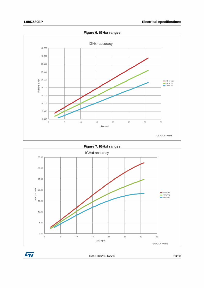
dIIGHxr Charge current accuracyVS = 13.5 V; VSHx = 0; VGHx = 1V
See Figure 6
dIIGHxf Discharge current accuracyVS = 13.5 V; VSHx = 0; VGHx = 2 V
See Figure 7
VDSHxrSW
Switching Voltage (VS - VSH) between current mode and switch mode (rising)
VS = 13.5 V 1.5 V
VTDSHxf(2)
Trigger Voltage to sample the VGSH for switching between switch mode and current mode (falling)
VS = 13.5 V; VGHx = 4 V 1.5 V
VTGSHxacc(2)
Sampled trigger voltage accuracy
VS = 13.5 V; VSHx = 0 1 V
t0GHxr Rise time (switch mode)VS = 13.5 V; VSHx = 0; RG = 0 ; CG = 2.7 nF
45 ns
t0GHxf Fall time (switch mode)VS = 13.5 V; VSHx = 0; RG = 0 ; CG = 2.7 nF
85 ns
t0GLxr Rise timeVS = 13.5 V; VSLx = 0; RG = 0 ; CG = 2.7 nF
45 ns
t0GLxf Fall timeVS = 13.5 V; VSLx = 0; RG = 0 ; CG = 2.7 nF
85 ns
tCCPProgrammable cross-current protection time
0.1 5 µs
fPWMH PWMH switching frequency(1)VS = 13.5 V; VSLx = 0; RG = 0 ; CG = 2.7 nF; PWMH - duty cycle = 50 %
50 kHz
1. Without cross-current protection time tCCP
2. Parameter not tested, typical value validated by characterization.
Table 16. Gate drivers for the external Power-MOS switching times
Symbol Parameter Test condition Min. Typ. Max. Unit
DocID18260 Rev 6 23/68
L99DZ80EP Electrical specifications
67
Figure 6. IGHxr ranges
Figure 7. IGHxf ranges

Electrical specifications L99DZ80EP
24/68 DocID18260 Rev 6
Figure 8. H-driver delay times
Table 17. Drain source monitoring
Symbol Parameter Test condition Min. Typ. Max. Unit
VSCd1 Drain-source threshold voltage VS = 13.5 V 0.3 0.5 0.7 V
VSCd2 Drain-source threshold voltage VS = 13.5 V 0.8 1 1.2 V
VSCd3 Drain-source threshold voltage VS = 13.5 V 1.2 1.5 1.8 V
VSCd4 Drain-source threshold voltage VS = 13.5 V 1.6 2 2.4 V
tSCd Drain-source monitor filter time 3 5.5 8 µs
tscsDrain-source comparator settling time
VS = 13.5 V; VSH = jump from GND to VS
— 5 µs
DocID18260 Rev 6 25/68
L99DZ80EP Electrical specifications
67
2.8 Electrochrome mirror driver
Table 18. Open-load monitoring
Symbol Parameter Test condition Min. Typ. Max. Unit
VODSLLow-side drain-source monitor low off-threshold voltage
VSLx = 0 V; VS = 13.5 V 0.14 * VS 0.18 * VS 0.21 * VS V
VODSHLow-side drain-source monitor high off-threshold voltage
VSLx = 0 V; VS = 13.5 V 0.75 * VS 0.85 * VS 0.95 * VS V
VOLSHxOutput voltage of selected SHx in open-load test mode
VSLx = 0 V; VS = 13.5 V 0.5 * VS V
RpdOL
Pull-down resistance of the non-selected SHx pin in open-load mode
VSLx = 0 V; VS = 13.5 V; VSHX = 4.5 V
20 k
TOL Open-load filter time 2 ms
Table 19. Electrochrome mirror driver
Symbol Parameter Test condition Min. Typ. Max. Unit
VCTRLmax Maximum EC-control voltageBit0 = 1 control reg. 2(1) 1.4 1.6 V
Bit0 = 0 control reg. 2(1) 1.12 1.28 V
DNLECV(2) Differential non linearity -1 1 LSB(3)
IdVECVIVoltage deviation between target and ECV
dVECV = Vtarget(4) - VECV;
IIECDRI < 1 µA-5 % -
1LSB(3)+5 % +1LSB(3) mV
dVECVnr Difference voltage between target and ECV sets flag if VECV is
below itdVECV = Vtarget
(4) - VECV; toggle bitx = 1 status reg. x
120 mV
dVECVhi above it -120 mV
tFECVNR ECVNR filter time 32 µs
tFECVHI ECVHI filter time 32 µs
VECDRminHIGHOutput voltage range
IECDR = -10 µA 4.5 5.5 V
VECDRmaxLOW IECDR = 10 µA 0 0.7 V
IECDR Current into ECDR
Vtarget(4) > VECV + 500 mV;
VECDR = 3.5 V-100 -10 µA
Vtarget(4) < VECV - 500 mV;
VECDR = 1.0 V; Vtarget = 0 V; VECV = 0.5 V
10 100 µA
Recdrdis
Pull-down resistance at ECDR in fast discharge mode and while EC-mode is off
VECDR = 0.7 V; ECON = ‘1’; EC<5:0> = 0 or ECON = ‘0’
10 k
DNLECFD(2) Differential Non Linearity -1 1 LSB(3)
IdVECFDIVoltage deviation between target and ECFD
dVECFD = Vtarget(4) - VECFD;
IECFD < TBD mA-5 %-
1LSB(3)+5 %+1LSB(3) mV

Electrical specifications L99DZ80EP
26/68 DocID18260 Rev 6
dVECFDnr(5)
Difference voltage between target and ECFD sets flag if VECFD is
below itdVECFD = Vtarget
(4) - VECFD; toggle status bit ECV_VNR = ’1‘
120 mV
dVECFDhi above it dVECFD = Vtarget
(4) - VECFD; Toggle status bit ECV_VH = ‘1’I
-120 mV
1. Bit ECV_HV ='1' or ‘0’: ECV voltage, where IIECDR can change sign
2. ECV and ECFD share same DAC circuit (see Figure 20, Figure 21).
3. 1 LSB (least significant bit) = 23.8mVtyp
4. Vtarget is set by bits EC<5:0> and bit ECV_HV; tested for each individual bit
5. Not tested since pulling pin ECFD to a low voltage against the internal source follower may lead to an overcurrent at pin ECFD HS.
Table 19. Electrochrome mirror driver (continued)
Symbol Parameter Test condition Min. Typ. Max. Unit

DocID18260 Rev 6 27/68
L99DZ80EP Electrical specifications
67
2.9 SPI / logic – electrical characteristics
The voltages are referred to ground and currents are assumed positive, when the current flows into the pin. 6V VS 18 V, 4.75 V VCC 5.5 V; all outputs open;Tj = -40 °C to 150 °C, unless otherwise specified.
Table 20. Delay time from Standby to Active mode
Symbol Parameter Test condition Min Typ Max Unit
tset Delay time
Switching time from standby to active mode. Time until output drivers are enabled after CSN going to high and set bit 0 = 1 of control register 0.
250 310 410 µs
twakup Wake-up time
Switching from standby to active mode. Time after the first falling edge of CSN until the first positive CLK edge, which latches EN = 1 correctly into the device
— 20 µs
tawake Stay awake time
Switching from standby to active mode. After the first rising edge of CSN a second SPI frame with EN = 1 is correctly recognized
— 256 µs
Table 21. Inputs: DI, CSN, CLK, DIR and PWMH
Symbol Parameter Test condition Min Typ Max Unit
Inputs: CSN, CLK, DI, DIR, PWMH
VIL Input voltage low level VS = 13.5 V; VCC = 5.0 V 0.3 * VCC V
VIH Input voltage high level VS = 13.5 V; VCC = 5.0 V 0.7 * VCC V
VIHYS Input hysteresis VS = 13.5 V; VCC = 5.0 V 500 mV
RCSN in CSN pull-up resistorVS = 13.5 V; VCC = 5.0 V; 0 V VCSN 0.7 * VCC
60 110 215 k
RCLK in CLK pull-down resistorVS = 13.5 V; VCC = 5.0 V; 0.3 * VCC VCLK VCC
60 110 215 k
RDI in DI pull-down resistorVS = 13.5 V; VCC = 5.0 V; 0.3 * VCC VDI VCC
60 110 215 k
RDIR DIR pull-down resistorVS = 13.5 V; VCC = 5.0 V; 0.3 * VCC VDIR VCC
60 110 215 k
RPWMH PWMH pull-down resistorVS = 13.5 V; VCC = 5.0 V; 0.3 * VCC VPWMH VCC
60 110 215 k
Output: DO
VOL Output voltage low levelIOL = 5 mA; VS = 13.5 V; VCC = 5.0 V
0.3 * VCC V
VOH Output voltage high levelIOH = -5 mA; VS = 13.5 V; VCC = 5.0 V
0.7 * VCC V
IDOLK 3-state leakage current VCSN = VCC; 0 < VDO < VCC -10 10 µA

Electrical specifications L99DZ80EP
28/68 DocID18260 Rev 6
For definition of the parameters please see Figure 9, Figure 10 and Figure 11.
Table 22. AC-Characteristics
Symbol Parameter Test condition Min. Typ. Max. Unit
COUT(1)
1. Value of input capacity is not measured in production test. Parameter guaranteed by design.
Output capacitance (DO)
— — 10 pF
CIN(1) Input capacitance (DI,
CSN, CLK, DIR, PWMH)— — 10 pF
Table 23. Dynamic characteristics
Symbol Parameter Test condition Min. Typ. Max. Unit
tCSNQVLDO enable from 3-state to low level
CDO = 100 pF; IDO = 1 mA; pull-up load to VCC; VS = 13.5 V; VCC = 5 V
100 250 ns
tCSNQVHDO enable from 3-state to high level
CDO = 100pF; IDO = -1 mA;pull-down load to GND; VS = 13.5 V; VCC = 5 V
100 250 ns
tCSNQTLDO disable from low level to 3-state
CDO = 100pF; IDO = 4 mA;pull-up load to VCC; VS = 13.5 V; VCC = 5 V
380 450 ns
tCSNQTHDO disable from high level to 3-state
CDO = 100 pF; IDO = -4 mA; pull-down load to GND; VS = 13.5 V; VCC = 5 V
380 450 ns
tCLKQV CLK falling until DO validVDO < 0.3 * VCC or VDO > 0.7 * VCC; CDO = 100 pF; VS = 13.5 V; VCC = 5 V
50 250 ns
tSCSNCSN setup time, CSN low before rising edge of CLK
VS = 13.5 V; VCC = 5 V 400 ns
tSDIDI setup time, DI stable before rising edge of CLK
VS = 13.5 V; VCC = 5 V 200 ns
TCLK Clock Period VS = 13.5 V; VCC = 5 V 1000 ns
tHCLK minimum CLK high time VS = 13.5 V; VCC = 5 V 115 ns
tLCLK minimum CLK low time VS = 13.5 V; VCC = 5 V 115 ns
tHCSN minimum CSN high time VS = 13.5 V; VCC = 5 V 4 µs
tSCLKCLK setup time before CSN rising
VS = 13.5 V; VCC = 5 V 400 ns
tr DO DO rise timeCDO = 100 pF; VS = 13.5 V; VCC = 5 V
80 140 ns
tf DO DO fall timeCDO = 100 pF; VS = 13.5 V; VCC = 5 V
50 100 ns

DocID18260 Rev 6 29/68
L99DZ80EP Electrical specifications
67
Figure 9. SPI timing parameters
tr inrise time of input signalDI, CLK, CSN
VS = 13.5 V; VCC = 5 V 100 ns
tf infall time of input signalDI, CLK, CSN
VS = 13.5 V; VCC = 5 V 100 ns
Table 23. Dynamic characteristics (continued)
Symbol Parameter Test condition Min. Typ. Max. Unit

Electrical specifications L99DZ80EP
30/68 DocID18260 Rev 6
Figure 10. SPI input and output timing parameters
Figure 11. SPI delay description

DocID18260 Rev 6 31/68
L99DZ80EP Electrical specifications
67
Figure 12. Power-output (OUT<11:1>, ECV, ECFD) timing
Table 24. Watchdog
Symbol Parameter Test condition Min. Typ. Max. Unit
TCWDTO Watchdog time out 50 64 100 ms

Application information L99DZ80EP
32/68 DocID18260 Rev 6
3 Application information
3.1 Dual power supply: VS and VCC
The power supply voltage VS supplies the power drivers and the Power-MOS gate drivers. For supplying the high-side drivers for the power- and gate-driver outputs, an internal charge-pump is used. The SPI interface and the logic circuitry is supplied by VCC.
Due to the independent VCC supply the control and status information are not lost, if there are spikes or glitches on the power supply voltage.
3.2 Wake up and Active mode/standby mode
After power up of VS and VCC the device operates in standby-mode. Pulling the signal CSN to low level wakes the device up and the analog part is activated (active mode). After at least 10 µs, the first SPI communication is valid and the EN-bit can be used to set the EN-mode.
The device can be set into active mode writing a ‘1’ into the EN-register. If the EN-register is not set to ‘1’, the device goes back to standby mode typical 256 µs after the rising edge of CSN and all latched data are cleared. In standby mode the current at VS (VCC) is less than 6 µA (5 µA) for CSN = high (DO in 3-state). It is recommended to switch all outputs off before entering standby mode.
3.3 Charge pump
The charge pump uses two external capacitors, which are switched with a frequency of typically 125 kHz. The output of the charge pump has a current limitation. In standby mode and after a thermal shutdown has been triggered the charge pump is disabled. If the charge pump output voltage remains too low for longer than TCP, the power-MOS outputs, the EC-control are switched off and the H-Bridge gate drivers are switched to resistive low. The CP_LOW bit has to be cleared through a software reset to reactivate the drivers.
3.4 Diagnostic functions
All diagnostic functions (overcurrent, open-load, power supply overvoltage /undervoltage, temperature warning and thermal shutdown) are internally filtered. The condition has to be valid for at least the associated filter time before the corresponding status bit in the status registers is set. The filters are used to improve the noise immunity of the device. The open-load and temperature warning functions are intended for information purpose and do not change the state of the output drivers. On contrary, the overcurrent condition disables the corresponding driver and thermal shutdown disables all drivers. Without setting the overcurrent recovery bits in the input data register, the microcontroller has to clear the overcurrent status bits to reactivate the corresponding drivers.

DocID18260 Rev 6 33/68
L99DZ80EP Application information
67
3.5 Overvoltage and undervoltage detection at VS
If the power supply voltage VS rises above the overvoltage threshold VSOV_OFF, the outputs OUT1 to OUT11, ECDR, ECV, ECFD are switched to high impedance state, the charge pump is disabled and the H-Bridge gate drivers are switched into sink condition to protect the H-bridge and the load. When the voltage VS drops below the undervoltage threshold VSUV_OFF (UV-switch-OFF voltage), the output stages are switched to high impedance to avoid the operation of the power devices without sufficient gate driving voltage (increased power dissipation). If the supply voltage VS recovers to normal operating voltage, the charge pump is switched on again, the CP_LOW bit is cleared and the output stages return to the programmed state. If the undervoltage/overvoltage recovery disable bit is set, the automatic turn-on of the drivers is deactivated.
If the undervoltage/overvoltage recovery disable bit (OV_UV_RD) is set, the microcontroller needs to clear the status bits to reactivate the drivers. It is recommended to set OV_UV_RD bit to avoid a possible high current oscillation in case of a shorted output to GND and low battery voltage.
3.6 Overvoltage and undervoltage detection at VCC
At power-on (VCC increases from undervoltage to VPOROFF) the circuit is initialized by an internally generated power-on-reset (POR). If the voltage VCC decreases below the low threshold (VPORON), the outputs are switched to 3-state (high impedance) and the status registers are cleared. If the voltage at pin VCC increases above the VCC reset high threshold VVCCRESHU, the device enters the reset state, all outputs are switched off and all internal registers are cleared. After the voltage at pin VCC has decreased below VVCCRESHL, the device enters normal operating mode again and the internal registers are reset.
3.7 Temperature warning and shutdown
If the junction temperature rises above the temperature warning threshold (TjTW), a temperature warning flag is set after the temperature warning filter time (Tjtft) and can be read via SPI. If the junction temperature increases above the temperature shutdown threshold (TjTS), the thermal shutdown bit is set and the power transistors of all output stages are switched off to protect the device after the thermal shutdown filter time. The gates of the H-Bridge are discharged by the ‘Resistive Low’ mode.
The temperature warning and thermal shutdown flags are latched and must be cleared by the microcontroller. This is done by a read and clear command on an arbitrary register, because both bits are part of the global status register.
After these bits have been cleared, the output stages are reactivated. If the temperature is still above the thermal warning threshold, the thermal warning bit is set after Tjtft. Once this bit is set and the temperature is above the temperature shutdown threshold, temperature shutdown is detected after Tjtft and the outputs are switched off. Therefore the minimum time after which the outputs are switched off after the bits have been cleared in case the temperature is still above the thermo-shutdown threshold is twice the thermo-warning/-shutdown filter time Tjtft.

Application information L99DZ80EP
34/68 DocID18260 Rev 6
3.8 Inductive loads
Each half bridge is built by internally connected high- and low-side power DMOS transistors. Due to the built-in reverse diodes of the output transistors, inductive loads can be driven at the outputs OUT1 to OUT6 without external freewheeling diodes. The high-side drivers OUT7 to OUT11 are intended to drive resistive loads. Therefore only a limited energy (E < 1 mJ) can be dissipated by the internal ESD-diodes in freewheeling condition. For inductive loads (L > 100 µH) an external freewheeling diode connected between GND and the corresponding output is required. The low side driver at ECV does not have a freewheel diode built into the device.
3.9 Open-load detection
The open load detection monitors the load current in each activated output stage. If the load current is below the open load detection threshold for at least tFOL the corresponding open-load bit is set in the status register. Due to mechanical/electrical inertia of typical loads a short activation of the outputs (e.g. 3 ms) can be used to test the open load status without changing the mechanical/electrical state of the loads.
3.10 Overcurrent detection
In case of an overcurrent condition, a flag is set in the status register. If the overcurrent signal is valid for at least TFOC, the overcurrent flag is set and the corresponding driver is switched off to reduce the power dissipation and to protect the integrated circuit. If the overcurrent recovery bit of the output is cleared, the microcontroller has to clear the status bits to reactivate the corresponding driver.
3.11 Current monitor
The current monitor output sources a current image at the current monitor output, which has three fixed ratios of the instantaneous current of the selected high-side driver. Outputs with a resistance of 500 mand higher have a ratio of 1/2000, except for OUT8, which has a ratio of 1/6500, and those with a lower resistance one of 1/10000. The signal at output CM is blanked after switching on the driver until correct settlement of the circuitry. The bits CM_SEL<3:0> define which of the outputs are multiplexed to the current monitor output CM. The current monitor output allows a more precise analysis of the actual state of the load rather than the detection of an open- or overload condition. For example, it can be used to detect the motor state (starting, free running, stalled). Moreover, it is possible to control the power of the defroster more precisely by measuring the load current. The current monitor output is enabled after the current-monitor blanking time, when the selected output is switched on. If this output is off, the current monitor output is in high-impedance mode.
3.12 PWM mode of the power outputs
Each driver has a corresponding PWM enable bit, which can be programmed by the SPI interface. If the PWM enable bit is set, the output is controlled by the logically AND-combination of an internally generated PWM signal and the output control bit of the corresponding driver. The PWM-Frequency of all outputs can be programmed to either 122 Hz of 244 Hz typically. The on-duty-cycle is set by the four 7-bit registers, which control

DocID18260 Rev 6 35/68
L99DZ80EP Application information
67
one PWM counter each. Therefore the maximum on-time is 100% - 1 LSB. 1 LSB = 100/128 %. Which output uses which corresponding PWM driver can be seen in the SPI register definition. When programming a specific duty-cycle, the output on/off times as well as the slopes must be taken into account.
3.13 Cross-current protection
The six half-brides of the device are crosscurrent protected by an internal delay time. If one driver (LS or HS) is turned off, the activation of the other driver of the same half bridge is automatically delayed by the crosscurrent protection time. After the crosscurrent protection time is expired the slew-rate limited switch-off phase of the driver is changed to a fast turn-off phase and the opposite driver is turned-on with slew-rate limitation. Due to this behavior, it is always guaranteed that the previously activated driver is completely turned off before the opposite driver starts to conduct
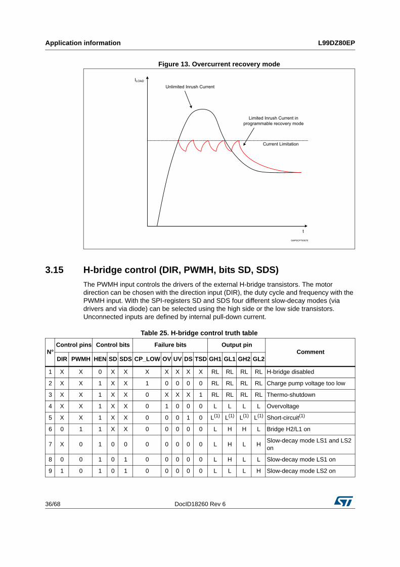
3.14 Programmable soft-start function to drive loads with higher inrush current
Loads with start-up currents higher than the overcurrent limits (e.g. inrush current of lamps, Start current of motors and cold resistance of heaters) can be driven by using the programmable softstart function (i.e. overcurrent recovery mode). Each driver has a corresponding overcurrent recovery bit. If this bit is set, the device automatically switches the outputs on again after a programmable recovery time. The duty cycle in overcurrent condition can be programmed by the SPI interface to about 12 % or 25 %. The PWM modulated current provides sufficient average current to power up the load (e.g. heat up the bulb) until the load reaches operating condition. The PWM frequency settles at 1.7 kHz and 3 kHz. The device itself cannot distinguish between a real overload and a non linear load like a light bulb. A real overload condition can only be qualified by time. For overload detection the microcontroller can switch on the light bulbs by setting the overcurrent recovery bit for the first e.g. 50 ms. After clearing the recovery bit the output is automatically switched off, if the overload condition remains. This overcurrent detection procedure has to be followed in order to make it possible to switch on the low side driver of a bridge output, if the associated high-side driver has been used in recovery mode before.
Application information L99DZ80EP
36/68 DocID18260 Rev 6
Figure 13. Overcurrent recovery mode
3.15 H-bridge control (DIR, PWMH, bits SD, SDS)
The PWMH input controls the drivers of the external H-bridge transistors. The motor direction can be chosen with the direction input (DIR), the duty cycle and frequency with the PWMH input. With the SPI-registers SD and SDS four different slow-decay modes (via drivers and via diode) can be selected using the high side or the low side transistors. Unconnected inputs are defined by internal pull-down current.
Table 25. H-bridge control truth table
N°Control pins Control bits Failure bits Output pin
CommentDIR PWMH HEN SD SDS CP_LOW OV UV DS TSD GH1 GL1 GH2 GL2
1 X X 0 X X X X X X X RL RL RL RL H-bridge disabled
2 X X 1 X X 1 0 0 0 0 RL RL RL RL Charge pump voltage too low
3 X X 1 X X 0 X X X 1 RL RL RL RL Thermo-shutdown
4 X X 1 X X 0 1 0 0 0 L L L L Overvoltage
5 X X 1 X X 0 0 0 1 0 L(1) L(1) L(1) L(1) Short-circuit(1)
6 0 1 1 X X 0 0 0 0 0 L H H L Bridge H2/L1 on
7 X 0 1 0 0 0 0 0 0 0 L H L HSlow-decay mode LS1 and LS2 on
8 0 0 1 0 1 0 0 0 0 0 L H L L Slow-decay mode LS1 on
9 1 0 1 0 1 0 0 0 0 0 L L L H Slow-decay mode LS2 on

DocID18260 Rev 6 37/68
L99DZ80EP Application information
67
3.16 H-bridge driver slew-rate control
The rising and falling slope of the drivers for the external high-side Power-MOS can be slew rate controlled. If this mode is enabled the gate of the external high-side Power-MOS is driven by a current source instead of a low-impedance output driver switch as long as the drain-source voltage over this Power-MOS is below the switch threshold. The current is programmed using the bits SLEW<4:0>, which represent a binary number. This number is multiplied by the minimum current step. This minimum current step is the maximum source-/sink-current (IGHxrmax / IGHxfmax) divided by 31. Programming SLEW<4:0> to 0 disables the slew rate control and the output is driven by the low-impedance output driver switch.
10 1 1 1 X X 0 0 0 0 0 H L L H Bridge H1/L2 on
11 X 0 1 1 0 0 0 0 0 0 H L H LSlow-decay mode HS1 and HS2 on
12 0 0 1 1 1 0 0 0 0 0 L L H L Slow-decay mode HS2 on
13 1 0 1 1 1 0 0 0 0 0 H L L L Slow-decay mode HS1 on
1. Only the half-bridge (low and high-side), in which one MOSFET is in short circuit condition is switched off. Both MOSFETs of the other half-bridge remain active and driven by DIR and PWMH
Table 25. H-bridge control truth table (continued)
N°Control pins Control bits Failure bits Output pin
CommentDIR PWMH HEN SD SDS CP_LOW OV UV DS TSD GH1 GL1 GH2 GL2

Application information L99DZ80EP
38/68 DocID18260 Rev 6
Figure 14. H-bridge GSHx slope
3.17 Resistive low
The resistive output mode protects the L99DZ80EP and the H-bridge in the standby mode and in some failure modes (thermal shut down (TSD), charge pump low (CP_LOW) and stuck-at-‘1’ at pin DI). When a gate driver changes into the resistive output mode due to a failure a sequence is started. In this sequence the concerning driver is switched into sink condition for 32 µs to 64 µs to ensure a fast switch-off of the H-bridge transistor. If slew rate control is enabled, the sink condition is slew-rate controlled. Afterwards the driver is switched into the resistive output mode (resistive path to source).
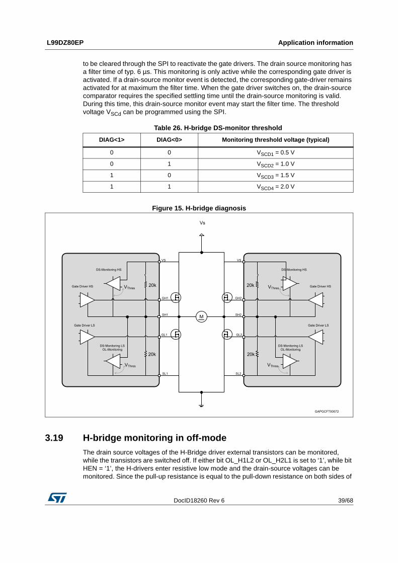
3.18 Short circuit detection/drain source monitoring
The drain source voltage of each activated external MOSFET of the H-bridge is monitored by comparators to detect shorts to ground or battery. If the voltage-drop over the external MOSFET exceeds the threshold voltage VSCd for longer than the short current detection time tSCd the corresponding gate driver switches the external MOSFET off and the corresponding drain source monitoring flag (DS_MON[3:0]) is set. The DS_MON bits have
DocID18260 Rev 6 39/68
L99DZ80EP Application information
67
to be cleared through the SPI to reactivate the gate drivers. The drain source monitoring has a filter time of typ. 6 µs. This monitoring is only active while the corresponding gate driver is activated. If a drain-source monitor event is detected, the corresponding gate-driver remains activated for at maximum the filter time. When the gate driver switches on, the drain-source comparator requires the specified settling time until the drain-source monitoring is valid. During this time, this drain-source monitor event may start the filter time. The threshold voltage VSCd can be programmed using the SPI.
Figure 15. H-bridge diagnosis
3.19 H-bridge monitoring in off-mode
The drain source voltages of the H-Bridge driver external transistors can be monitored, while the transistors are switched off. If either bit OL_H1L2 or OL_H2L1 is set to ‘1’, while bit HEN = ‘1’, the H-drivers enter resistive low mode and the drain-source voltages can be monitored. Since the pull-up resistance is equal to the pull-down resistance on both sides of
Table 26. H-bridge DS-monitor threshold
DIAG<1> DIAG<0> Monitoring threshold voltage (typical)
0 0 VSCD1 = 0.5 V
0 1 VSCD2 = 1.0 V
1 0 VSCD3 = 1.5 V
1 1 VSCD4 = 2.0 V

Application information L99DZ80EP
40/68 DocID18260 Rev 6
the bridge a voltage of 2/3 VS on the pull-up high-side and 1/3 VS on the low side is expected, if they drive a low-resistive inductive load (e.g. motor). If the drain source voltage on each of these Power-MOS is less than 1/6 VS, the drain-source monitor bit of the associated driver is set.
In case of a short to ground the drain-source monitor bits of both low-side gate drivers are set. A short to VS can be diagnosed by setting the “H-Bridge OL high threshold (H-OLTH HIGH)” bit to one.
Figure 16. H-bridge open-load detection (no open-load detected)
Figure 17. H-bridge open-load detection (open-load detected)

DocID18260 Rev 6 41/68
L99DZ80EP Application information
67
Figure 18. H-bridge open-load detection (short to ground detected)
Figure 19. H-bridge open-load detection with H-OLTH HIGH = ‘1’ (short to VS detected)
3.20 Programmable cross current protection
Both external MOSFET transistors in one half-bridge are disabled for the cross-current protection time (tCCP) after one MOSFET inside this halfbridge is switched off to prevent current flowing from the high-side to the low-side MOSFET.
The cross current protection time tCCP can be programmed by SPI using bits COPT<3:0>.

Application information L99DZ80EP
42/68 DocID18260 Rev 6
3.21 Controller of electrochromic glass
The voltage of an electrochromic element connected at pin ECV can be controlled to a target value, which is set by the bits EC<5:0>. Setting bit ECON enables this function. An on-chip differential amplifier and an external MOS source follower, with its gate connected to pin ECDR, and which drives the electrochrome mirror voltage at pin ECV, form the control loop. The drain of the external MOS transistor is supplied by OUT10. A diode from pin ECV (anode) to pin ECDR (cathode) has been placed on the chip to protect the external MOS source follower. A capacitor of at least 5 nF has to be added to pin ECDR for loop-stability. The target voltage is binary coded with a full-scale range of 1.5 V. If Bit EC_HV s set to '0', the maximum controller output voltage is clamped to 1.2 V without changing the resolution of bits EC<5:0>.
When programming the ECVLS driver to on-state, the voltage at pin ECV is pulled to ground by a 1.6 low-side switch until the voltage at pin ECV is less than dVECVhi higher than the target voltage (fast discharge). The status of the voltage control loop is reported via SPI. Bit ECV_VHI is set, if the voltage at pin ECV is higher, whereas Bit ECV_VNR in the same status register is set, if the voltage at pin ECV is lower than the target value. Both status bits are valid, if they are stable for at least the ECVHI/ECVNR – filter time and are not latched. Since OUT10 is the output of a high-side driver, it contains the same diagnose functions as the other high-side drivers (e.g. during an overcurrent detection, the control loop is switched off). In electrochrome mode, OUT10 cannot be controlled by PWM mode. For EMS reasons, the loop capacitor at pin ECDR as well as the capacitor between ECV and GND have to be placed to the respective pins as close as possible (see Figure 20 for details).
Table 27. Cross-current protection time
COPT<3> COPT<2> COPT<1> COPT<0> Min Typ Max unit
0 0 0 0 150 250 360 ns
0 0 0 1 390 500 670 ns
0 0 1 0 590 750 980 ns
0 0 1 1 800 1000 1280 ns
0 1 0 0 1000 1250 1600 ns
0 1 0 1 1210 1500 1910 ns
0 1 1 0 1420 1750 2220 ns
0 1 1 1 1630 2000 2540 ns
1 0 0 0 1830 2250 2850 ns
1 0 0 1 2050 2500 3120 ns
1 0 1 0 2250 2750 3450 ns
1 0 1 1 2460 3000 3760 ns
1 1 0 0 2660 3250 4100 ns
1 1 0 1 2880 3500 4370 ns
1 1 1 0 3080 3750 4680 ns
1 1 1 1 3200 4000 5000 ns
DocID18260 Rev 6 43/68
L99DZ80EP Application information
67
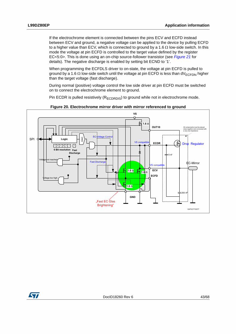
If the electrochrome element is connected between the pins ECV and ECFD instead between ECV and ground, a negative voltage can be applied to the device by pulling ECFD to a higher value than ECV, which is connected to ground by a 1.6 low-side switch. In this mode the voltage at pin ECFD is controlled to the target value defined by the register EC<5:0>. This is done using an on-chip source-follower transistor (see Figure 21 for details). The negative discharge is enabled by setting bit ECND to ‘1’.
When programming the ECFDLS driver to on-state, the voltage at pin ECFD is pulled to ground by a 1.6 low-side switch until the voltage at pin ECFD is less than dVECFDhi higher than the target voltage (fast discharge).
During normal (positive) voltage control the low side driver at pin ECFD must be switched on to connect the electrochrome element to ground.
Pin ECDR is pulled resistively (RECDRDIS) to ground while not in electrochrome mode.
Figure 20. Electrochrome mirror driver with mirror referenced to ground

Application information L99DZ80EP
44/68 DocID18260 Rev 6
Figure 21. Electrochrome mirror driver with mirror referenced to ECFD for negative discharge
3.22 Watchdog
The watchdog monitors the µC during normal operation within a nominal trigger cycle of 60ms. The watchdog is triggered by toggling the watchdog bit, which restarts the watchdog timer (i.e. content of the watchdog trigger bit has to be inverted). If no watchdog bit inversion has been occurred during the watchdog time-out time TWDTO the H-bridge drivers switch into resistive-low condition, all power outputs are switched off, the electrochrome driver is disabled and the device enters standby mode.
DocID18260 Rev 6 45/68
L99DZ80EP Functional description of the SPI
67
4 Functional description of the SPI
4.1 General description
The SPI complies with Standard ST-SPI Interface Version 3.1.
Its communication is based on a Serial Peripheral Interface structure using CSN (Chip Select Not), DI (Serial Data In), DO (Serial Data Out/Error) and CLK (Serial Clock) signal lines.
4.1.1 Chip Select Not (CSN)
The CSN input pin is used to select the serial interface of this device. When CSN is high, the output pin (DO) is in high impedance state. A low signal wakes up the device and a serial communication can be started. The state when CSN is going low until the rising edge of CSN is called a communication frame.
4.1.2 Serial Data In (DI)
The DI input pin is used to transfer data serially into the device. The data applied to the DI is sampled at the rising edge of the CLK signal. A stuck-at ‘0’ or ‘1’ enters the standby mode.
4.1.3 Serial Clock (CLK)
The CLK input signal provides the timing of the serial interface. The Data Input (DI) is latched at the rising edge of Serial Clock CLK. The SPI can be driven by a micro controller with its SPI peripheral running in following mode: CPOL = 0 and CPHA = 0. Data on Serial Data Out (DO) is shifted out at the falling edge of the serial clock (CLK). The serial clock CLK must be active only during a frame (CSN low). Any other switching of CLK close to any CSN edge could generate set up/hold violations in the SPI logic of the device. The clock monitor counts the number of clock pulses during a communication frame (while CSN is low). If the number of CLK pulses does not correspond to the frame width indicated in the <SPI-frame-ID> (ROM address 03H) the frame is ignored and the <frame error> bit in the <Global Status Byte> is set.
Note: Due to this safety functionality, daisy chaining the SPI is not possible. Instead, a parallel operation of the SPI bus by controlling the CSN signal of the connected ICs is recommended.
4.1.4 Serial Data Out (DO)
The data output driver is activated by a logical low level at the CSN input and goes from high impedance to a low or high level depending on the global status bit 7 (Global Error Flag). The content of the selected status or control register is transferred into the data out shift register after the address bits have been transmitted. Each subsequent falling edge of the CLK shifts the next bit out.
4.1.5 SPI communication flow
At the beginning of each communication the master can read the contents of the <SPIframe-ID> register (ROM address 03H) of the slave device.

Functional description of the SPI L99DZ80EP
46/68 DocID18260 Rev 6
This 8-bit register indicates the SPI frame length (24 bit) and the availability of additional features. Each communication frame consists of a command byte, which is followed by two data bytes.
The data returned on DO within the same frame always starts with the <Global Status> Byte. It provides general status information about the device. It is followed by two data bytes (i. e. ‘In-frame-response’).
For write cycles the <Global Status> Byte is followed by the previous content of the addressed register.
Figure 22. Write and read SPI

DocID18260 Rev 6 47/68
L99DZ80EP Functional description of the SPI
67
4.2 Command byte
OCx: operation code
Ax: address
Dx: data bit
Each communication frame starts with a command byte. It consists of an operating code which specifies the type of operation (<Read>, <Write>, <Read and Clear>, <Read Device Information>) and a 6 bit address. If less than 6 bits are required, the remaining bits are unused but are reserved.
4.2.1 Operation code definition
The <Write Mode> and <Read Mode> operations allow access to the RAM of the device.
A <Read and Clear Mode> operation is used to read a status register and subsequently clear its content.
The <Read Device Information> allows access to the ROM area which contains device related information such as <ID-Header>, <Product Code>, <Silicon Version> and <SPI-frame-ID>.
4.3 Device memory map
Table 28. Command byte
Command byte Data byte 1 Data byte 2
Bit 23 22 21 20 19 18 17 16 15 14 13 12 11 10 9 8 7 6 5 4 3 2 1 0
Name OC1 OC0 A5 A4 A3 A2 A1 A0 D15 D14 D13 D12 D11 D10 D9 D8 D7 D6 D5 D4 D3 D2 D1 D0
Table 29. Operation code definition
OC1 OC0 Meaning
0 0 <Write Mode>
0 1 <Read Mode>
1 0 <Read and Clear Mode>
1 1 <Read Device Information>
Table 30. RAM memory map
Address Name Access Content
00h Control Register 0 Read/writeDevice enable, output bridge and H-bridge open-load control
01h Control Register 1 Read/write High-side/ low-side and electrochrome control
02h Control Register 2 Read/write Bridge recovery mode, PWM and electrochrome setup

Functional description of the SPI L99DZ80EP
48/68 DocID18260 Rev 6
03h Control Register 3 Read/writeHigh-side recovery mode, PWM setup and current-monitor selection
04h Control Register 4 Read/write H-bridge driver control
05h Control Register 5 Read/write PWM register
06h Control Register 6 Read/write PWM register
10h Status Register 0 Read/clearOutput bridge overcurrent and H-bridge drain-source diagnosis
11h Status Register 1 Read/clear Output bridge and H-bridge open-load diagnosis
12h Status Register 2 Read/clearHigh-side overcurrent/open-load and electrochrome diagnosis
13h Status Register 3 Read/clear VS and chargepump diagnosis
3Fh Configuration Reg. Read/write Mask bits in global status register
Table 31. ROM memory map
Address Name Access Content
00h ID Header Read only 4300h (ASSP ST_SPI)
01h Version Read only 0300h
02h Product Code 1 Read only 5200h (82 ST_SPI)
03h Product Code 2 Read only 4800h (H ST_SPI)
3Eh SPI-Frame ID. Read only 4200h SPI-Frame-ID (ST_SPI)
Table 30. RAM memory map (continued)
Address Name Access Content

DocID18260 Rev 6 49/68
L99DZ80EP SPI - control and status registers
67
5 SPI - control and status registers
Table 32. Global status byte
Bit 7 6 5 4 3 2 1 0
Name GL_ER CO_ER C_RESET TSD TW UOV_OC_DS OL NR
Reset 0 0 1 0 0 0 0 0
GL_ER: Global Error Flag. Failures of bits 6 to 0 are always linked to the Global Error Flag. This flag is set, if at least one of these bits indicates a failure. It is reflected via the DO pin while CSN is held low and no SPI clock signal is applied. This operation does not cause the Communication Error bit in the <Global Status> to be set. The signal TW bit3 and OL bit1can be masked.
CO_ER: Communication Error.If the number of clock pulses during the previous frame is not 24, the frame is ignored and this bit is set.
C_RESET: Chip RESET.If a stuck at ‘1’ on input DI during any SPI frame occurs, or if a Power On Reset (VCC monitor) occurs. C_RESET is reset (‘1’) with any SPI command. When C_RESET is active (‘0’), the gate drivers are switched off (resistive path to source). After a startup of the circuit C_RESET is active due to the power-up reset pulse. Therefore, the gate drivers are switched off. They can only be activated after the C_RESET has been reset by an SPI command.
TSD: Thermal shutdown. All gate drivers and the charge pump are switched off (resistive path to source). The TSD bit has to be cleared through a read and clear command to reactivate the gate drivers and the chargepump.
TW: Thermal Warning. This bit can be masked using the configuration register.
UOV_OC_DS: Logical OR of the filtered undervoltage/overvoltage, chargepump-low, overcurrent of the power outputs and the H-bridge drain-source monitor signals.
OL: Open-load. Logical OR of the filtered output driver open-load signals. This bit can be masked using the configuration register.
NR: Not Ready.After switching the device from standby mode to active mode an internal timer is started to allow the chargepump to settle before the outputs can be activated. This bit is cleared automatically after the startup time.

SPI - control and status registers L99DZ80EP
50/68 DocID18260 Rev 6
5.1 Control Register 0
5.2 Control Register 1
Table 33. Control Register 0
Bit Name Access Reset Content
15 OUT1_HS on/off Read/write 0
The corresponding output driver is activated, if this bit is set. Setting the PWM enable bit, the driver is only switched on, if the PWM timer enables it. An internal cross-current protection prevents, that both the low- and high-side of the half-bridges OUT1-OUT6 are switched on simultaneously.
14 OUT1_LS on/off Read/write 0
13 OUT2_HS on/off Read/write 0
12 OUT2_LS on/off Read/write 0
11 OUT3_HS on/off Read/write 0
10 OUT3_LS on/off Read/write 0
9 OUT4_HS on/off Read/write 0
8 OUT4_LS on/off Read/write 0
7 OUT5_HS on/off Read/write 0
6 OUT5_LS on/off Read/write 0
5 OUT6_HS on/off Read/write 0
4 OUT6_LS on/off Read/write 0
3 0 0
Reserved (must be set to ‘0’)2 0 0
1 0 0
0 EN Read/write 0The device is switched into active mode, if EN is ‘1’. It enters the standby mode, if the EN bit is ‘0’. In standby mode all bits are reset.
Table 34. Control Register 1
Bit Name Access Reset Content
15 OUT7_HS1 on/off Read/write 0
14 OUT7_HS2 on/off Read/write 0
13 OUT8_HS1 on/off Read/write 0
12 OUT8_HS2 on/off Read/write 0
11 OUT9_HS on/off Read/write 0
The corresponding output driver is activated, if this bit is set. Setting the PWM enable bit, the driver is only switched on, if the PWM timer enables it.
10 OUT10_HS on/off Read/write 0
9 OUT11_HS on/off Read/write 0
8 ECV_LS on/off Read/write 0
HS1 HS2 Mode
0 0 Off
0 1 Low on-resistance
1 0 High on-resistance
1 1 Off

DocID18260 Rev 6 51/68
L99DZ80EP SPI - control and status registers
67
5.3 Control Register 2
7 EC<5> Read/write 0
The reference voltage for the electrochrome voltage controller at pins ECV and ECFD is binary coded.
6 EC<4> Read/write 0
5 EC<3> Read/write 0
4 EC<2> Read/write 0
3 EC<1> Read/write 0
2 EC<0> Read/write 0
1 ECON Read/write 0The electrochrome control is activated by setting this bit to ‘1’. This enables the driver at pin ECDR and switches OUT10 directly on ignoring bit OUT10_HS on/off.
0 ECFD_LS on/off Read/write 0The corresponding output driver is activated, if this bit is set. Setting the PWM enable bit, the driver is only switched on, if the PWM timer enables it.
Table 34. Control Register 1 (continued)
Bit Name Access Reset Content
Table 35. Control Register 2
Bit Name Access Reset Content
15 OUT1_OCR Read/write 0
Setting this bit to high enables the overcurrent recovery mode for the corresponding output.
14 OUT2_OCR Read/write 0
13 OUT3_OCR Read/write 0
12 OUT4_OCR Read/write 0
11 OUT5_OCR Read/write 0
10 OUT6_OCR Read/write 0
9 ECV_OCR Read/write 0
8 ECND Read/write 0Setting this bit to ‘1’ puts the electrochrome controller into the negative discharge mode.
7 OUT1_PWM3 Read/write 0
Setting this bit to ‘1’ enables the PWM mode for the corresponding output.
6 OUT2_PWM1 Read/write 0
5 OUT3_PWM2 Read/write 0
4 OUT4_PWM1 Read/write 0
3 OUT5_PWM2 Read/write 0
2 OUT6_PWM3 Read/write 0
1 ECV_PWM4 Read/write 0
0 ECV_HV Read/write 0Setting this bit to ‘1’ sets the maximum electrochrome controller voltage to 1.5 V (typ.). A ‘0’ clamps it to 1.2V (typ.).

SPI - control and status registers L99DZ80EP
52/68 DocID18260 Rev 6
5.4 Control Register 3
Table 36. Control Register 3
Bit Name Access Reset Content
15 OUT7_OCR Read/write 0
Setting this bit to high enables the overcurrent recovery mode for the corresponding output.
14 OUT8_OCR Read/write 0
13 OUT9_OCR Read/write 0
12 OUT10_OCR Read/write 0
11 OUT11_OCR Read/write 0
10 OUT7_PWM1 Read/write 0
Setting this bit to ‘1’ enables the PWM mode for the corresponding output.
9 OUT8_PWM2 Read/write 0
8 OUT9_PWM3 Read/write 0
7 OUT10_PWM4 Read/write 0
6 OUT11_PWM4 Read/write 0
5 OCR_FREQ Read/write 0This bit defines the overcurrent recovery frequency (0: 1.7kHz (typ.) 1: 3kHz (typ.))
4 OV_UV_RD Read/write 0If this bit is set, the associated status bit has to be cleared after an overvoltage /undervoltage event to enable the output drivers again.
3 CM_SEL<3> Read/write 0
A current image of the selected binary coded output is multiplexed to the CM output. If a corresponding output does not exist, the current monitor is deactivated (especially ‘0000’).
2 CM_SEL<2> Read/write 0
1 CM_SEL<1> Read/write 0
0 CM_SEL<0> Read/write 0
CM_SEL<3:0> Selected output
0000 3-state
0001 OUT<1>
0010 OUT<2>
0011 OUT<3>
0100 OUT<4>
0101 OUT<5>
0110 OUT<6>
0111 OUT<7>
1000 OUT<8>
1001 OUT<9>
1010 OUT<10>
1011 OUT<11>
1100 Reserved
1101-1111 3-state
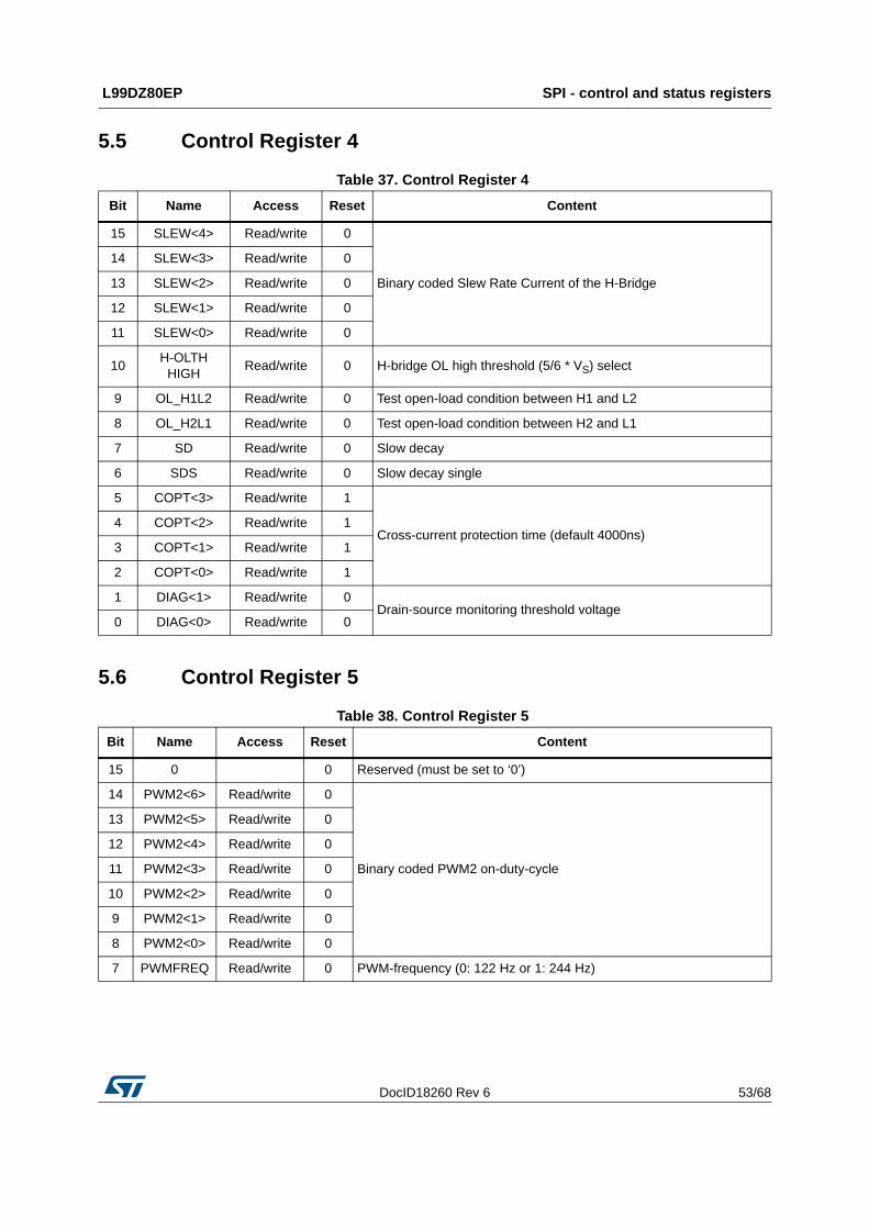
DocID18260 Rev 6 53/68
L99DZ80EP SPI - control and status registers
67
5.5 Control Register 4
5.6 Control Register 5
Table 37. Control Register 4
Bit Name Access Reset Content
15 SLEW<4> Read/write 0
Binary coded Slew Rate Current of the H-Bridge
14 SLEW<3> Read/write 0
13 SLEW<2> Read/write 0
12 SLEW<1> Read/write 0
11 SLEW<0> Read/write 0
10H-OLTH
HIGHRead/write 0 H-bridge OL high threshold (5/6 * VS) select
9 OL_H1L2 Read/write 0 Test open-load condition between H1 and L2
8 OL_H2L1 Read/write 0 Test open-load condition between H2 and L1
7 SD Read/write 0 Slow decay
6 SDS Read/write 0 Slow decay single
5 COPT<3> Read/write 1
Cross-current protection time (default 4000ns)4 COPT<2> Read/write 1
3 COPT<1> Read/write 1
2 COPT<0> Read/write 1
1 DIAG<1> Read/write 0Drain-source monitoring threshold voltage
0 DIAG<0> Read/write 0
Table 38. Control Register 5
Bit Name Access Reset Content
15 0 0 Reserved (must be set to ‘0’)
14 PWM2<6> Read/write 0
Binary coded PWM2 on-duty-cycle
13 PWM2<5> Read/write 0
12 PWM2<4> Read/write 0
11 PWM2<3> Read/write 0
10 PWM2<2> Read/write 0
9 PWM2<1> Read/write 0
8 PWM2<0> Read/write 0
7 PWMFREQ Read/write 0 PWM-frequency (0: 122 Hz or 1: 244 Hz)

SPI - control and status registers L99DZ80EP
54/68 DocID18260 Rev 6
5.7 Control Register 6
6 PWM1<6> Read/write 0
Binary coded PWM1 on-duty-cycle
5 PWM1<5> Read/write 0
4 PWM1<4> Read/write 0
3 PWM1<3> Read/write 0
2 PWM1<2> Read/write 0
1 PWM1<1> Read/write 0
0 PWM1<0> Read/write 0
Table 38. Control Register 5 (continued)
Bit Name Access Reset Content
Table 39. Control Register 6
Bit Name Access Reset Content
15 0 0 Reserved (must be set to ‘0’)
14 PWM4<6> Read/write 0
Binary coded PWM4 on-duty-cycle
13 PWM4<5> Read/write 0
12 PWM4<4> Read/write 0
11 PWM4<3> Read/write 0
10 PWM4<2> Read/write 0
9 PWM4<1> Read/write 0
8 PWM4<0> Read/write 0
7 0 0 Reserved (must be set to ‘0’)
6 PWM3<6> Read/write 0
Binary coded PWM3 on-duty-cycle
5 PWM3<5> Read/write 0
4 PWM3<4> Read/write 0
3 PWM3<3> Read/write 0
2 PWM3<2> Read/write 0
1 PWM3<1> Read/write 0
0 PWM3<0> Read/write 0

DocID18260 Rev 6 55/68
L99DZ80EP SPI - control and status registers
67
5.8 Configuration Register
5.9 Status Register 0
Table 40. Configuration Register
Bit Name Access Reset Content
15 0 0
Reserved (must be set to ‘0’)
14 0 0
13 0 0
12 0 0
11 0 0
10 0 0
9 0 0
8 0 0
7 0 0
6 HEN Read/write 0 A ‘1’ enables the H-bridge
5 MASK OL HS1 Read/write 0 Masks open-load of high-side 1 to global status register
4 MASK OL LS1 Read/write 0 Masks open-load of low-side 1 to global status register
3 MASK TW Read/write 0 Masks thermo warning to global status register
2 MASK EC OL Read/write 0 Masks open-load of ECV, ECFDHS, ECFDLS and OUT10
1 MASK OL Read/write 0 Masks all open-load diagnosis to global status register
0 WD Read/write 0 Watchdog
Table 41. Status Register 0
Bit Name Access Content
15 OUT1_HS OC Read/clear
Overcurrent status bit of the corresponding output driver. A ‘1’ indicates that an overcurrent has occurred.
14 OUT1_LS OC Read/clear
13 OUT2_HS OC Read/clear
12 OUT2_LS OC Read/clear
11 OUT3_HS OC Read/clear
10 OUT3_LS OC Read/clear
9 OUT4_HS OC Read/clear
8 OUT4_LS OC Read/clear
7 OUT5_HS OC Read/clear
6 OUT5_LS OC Read/clear
5 OUT6_HS OC Read/clear
4 OUT6_LS OC Read/clear

SPI - control and status registers L99DZ80EP
56/68 DocID18260 Rev 6
5.10 Status Register 1
3 DS_MON_HS<2> Read/clear
DS-Monitoring bit. A ‘1’ indicates that a drain-monitoring event (short-circuit or open-load) has occurred.
2 DS_MON_HS<1> Read/clear
1 DS_MON_LS<2> Read/clear
0 DS_MON_LS<1> Read/clear
Table 41. Status Register 0 (continued)
Bit Name Access Content
Table 42. Status Register 1
Bit Name Access Content
15 OUT1_HS OL Read/clear
Open-Load status bit of the corresponding output driver. A ‘1’ indicates that an open-load event has occurred.
14 OUT1_LS OL Read/clear
13 OUT2_HS OL Read/clear
12 OUT2_LS OL Read/clear
11 OUT3_HS OL Read/clear
10 OUT3_LS OL Read/clear
9 OUT4_HS OL Read/clear
8 OUT4_LS OL Read/clear
7 OUT5_HS_OL Read/clear
6 OUT5_LS OL Read/clear
5 OUT6_HS OL Read/clear
4 OUT6_LS OL Read/clear
3 0 Read
Reserved2 0 Read
1 0 Read
0 0 Read
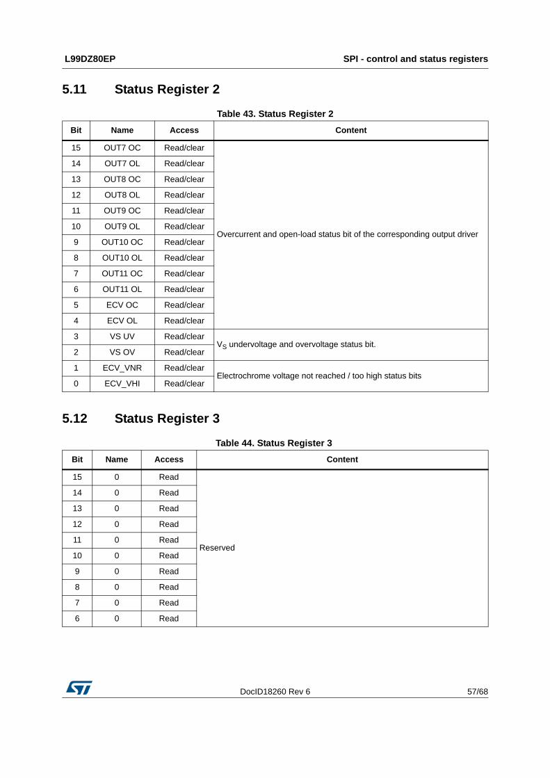
DocID18260 Rev 6 57/68
L99DZ80EP SPI - control and status registers
67
5.11 Status Register 2
5.12 Status Register 3
Table 43. Status Register 2
Bit Name Access Content
15 OUT7 OC Read/clear
Overcurrent and open-load status bit of the corresponding output driver
14 OUT7 OL Read/clear
13 OUT8 OC Read/clear
12 OUT8 OL Read/clear
11 OUT9 OC Read/clear
10 OUT9 OL Read/clear
9 OUT10 OC Read/clear
8 OUT10 OL Read/clear
7 OUT11 OC Read/clear
6 OUT11 OL Read/clear
5 ECV OC Read/clear
4 ECV OL Read/clear
3 VS UV Read/clearVS undervoltage and overvoltage status bit.
2 VS OV Read/clear
1 ECV_VNR Read/clearElectrochrome voltage not reached / too high status bits
0 ECV_VHI Read/clear
Table 44. Status Register 3
Bit Name Access Content
15 0 Read
Reserved
14 0 Read
13 0 Read
12 0 Read
11 0 Read
10 0 Read
9 0 Read
8 0 Read
7 0 Read
6 0 Read

SPI - control and status registers L99DZ80EP
58/68 DocID18260 Rev 6
5 ECFDH OC Read/clear
Overcurrent and open-load status bit of the corresponding output driver4 ECFDH OL Read/clear
3 ECFD OC Read/clear
2 ECFD OL Read/clear
1 0 Read Reserved
0 CP LOW Read/clear This bit indicates, that the charge pump voltage is too low
Table 44. Status Register 3 (continued)
Bit Name Access Content

DocID18260 Rev 6 59/68
L99DZ80EP Package and packing information
67
6 Package and packing information
6.1 ECOPACK® package
In order to meet environmental requirements, ST offers these devices in different grades of ECOPACK® packages, depending on their level of environmental compliance. ECOPACK® specifications, grade definitions and product status are available at: www.st.com. ECOPACK® is an ST trademark.
6.2 TQFP-64 mechanical data
Table 45. TQFP-64 mechanical data
SymbolMillimeters
Min. Typ. Max.
A 1,20
A1 0,05 0,15
A2 0,95 1,00 1,05
b 0,17 0,22 0,27
c 0,09 0,20
D 11,80 12,00 12,20
D1 9,80 10,00 10,20
D2(1)
1. The size of exposed pads is variable depending on lead frame design and pad size end user should verify "D2" and "E2" dimensions for each device application
5,85 6,00 6,15
D3 7,50
E 11,80 12,00 12,20
E1 9,80 10,00 10,20
E2(1) 5,85 6,00 6,15
E3 7,50
e 0,50
L 0,45 0,60 0,75
L1 1,00
k 0° 3,50° 7°
ccc 0,08

Package and packing information L99DZ80EP
60/68 DocID18260 Rev 6
Figure 23. TQFP-64 package dimension

DocID18260 Rev 6 61/68
L99DZ80EP Package and packing information
67
6.3 TQFP-64 packing information
The devices can be packed in tray or tape and reel shipments (see the Figure 1: Device summary on page 1 for packaging quantities).
Figure 24. TQFP-64 power lead-less tray shipment (no suffix) (part 1)

Package and packing information L99DZ80EP
62/68 DocID18260 Rev 6
Figure 25. TQFP-64 power lead-less tray shipment (no suffix) (part 2)

DocID18260 Rev 6 63/68
L99DZ80EP Package and packing information
67
Figure 26. TQFP-64 power lead-less tape and reel shipment (suffix “TR”) (part 1)

Package and packing information L99DZ80EP
64/68 DocID18260 Rev 6
Figure 27. TQFP-64 power lead-less tape and reel shipment (suffix “TR”) (part 2)

DocID18260 Rev 6 65/68
L99DZ80EP Revision history
67
7 Revision history
Table 46. Document revision history
Date Revision Change
20-Dec-2010 1 Initial release
10-Mar-2011 2
Updated Datasheet - production data list.
Updated following tables:
– Table 1: Device summary
– Table 2: Pin definitions and functions:
GH2, SH2, GL2, SL2: updated functions
– Table 7: Package thermal impedance
– Table 8: Supply:
IVCC(stby): set max value to TBD
– Table 13: Power outputs switching times:
td HL, td LH: updated parameter
– Table 31: ROM memory map:
updated content for address 01h
– Table 40: Configuration Register:
bit 5, 4, 3 and 1: updated contents
Updated following sections:
– Section 3.5: Overvoltage and undervoltage detection at VS
– Section 3.19: H-bridge monitoring in off-mode
– Section 3.20: Programmable cross current protection
Updated Figure 21: Electrochrome mirror driver with mirror referenced to ECFD for negative discharge
Added Section 6.3: TQFP-64 packing information

Revision history L99DZ80EP
66/68 DocID18260 Rev 6
06-Apr-2011 3
Table 8: Supply:
– IVCC(stby): changed TBD at 6 µA and updated VCC from 5.1 V t0 5.0 V; added test condition for VCC = 5.3 V
Table 9: Overvoltage and undervoltage detection:
– VVCCRESHU, VVCCRESHD: updated max value
– VVCCRES hysth: updated test condition
Table 12: On-resistance:
– IQLL: updated max value for OUT1-6 and typ, min, max for ECFD
Table 13: Power outputs switching times:
– td ON H: updated min value for all OUT except OUT7,8
– dVOUT/dt: updated min value
Table 15: Gate drivers for the external Power-MOS (H-bridge):
– IpdGSHx: removed row
– RGHx, RGLx: updated min, typ and max values
Table 18: Open-load monitoring:
– VODSL: added min and max values, updated typ value
– VODSH: added min and max values
Table 19: Electrochrome mirror driver:
– DNLECV, DNLECFD: added note
Table 20: Delay time from Standby to Active mode:
– tset: updated max value
Table 46. Document revision history (continued)
Date Revision Change

DocID18260 Rev 6 67/68
L99DZ80EP Revision history
67
16-Sep-2011 4
Updated Table 1: Device summary
Table 9: Overvoltage and undervoltage detection
– VSUV OFF: updated min value
Table 11: Charge pump
– VCP: updated test condition and max value
– ICP: updated max value
– ICPlim: updated min value
Table 12: On-resistance
– IQLH: updated min value
– IQLL: updated test condition
Table 13: Power outputs switching times
– td OFF L: updated max value
– td HL, td LH :updated min value
Table 14: Current monitoring
– |IOC1|, |IOC6|, |IOC4|, |IOC5|: updated max values
– |IOLD1|, |IOLD6|: updated min value
Table 15: Gate drivers for the external Power-MOS (H-bridge)
– RGHx, RGLx :updated min, typ and max values
Table 16: Gate drivers for the external Power-MOS switching times
– IGHxrmax, IGHxfmax, dIIGHxr, dIIGHxf: updated parameters; updated min, typ and max values
– tCCP: updated max value
– tCCPacc: removed row
– Table 17: Drain source monitoring:
– VSCd1, VSCd2, VSCd3, VSCd4: updated test contitions, min and vax values
– tSCd: updated min, typ and max values
– Table 20: Delay time from Standby to Active mode
– tset:updated min, typ and max values
Table 21: Inputs: DI, CSN, CLK, DIR and PWMH
– RCSN in,RCLK in, RDI in, RDIR, RPWMH:updated min, typ and max values
Updated Table 27: Cross-current protection time
22-Sep-2013 5 Updated Disclaimer.
23-12-2016 6
Updated cover page:
- Automotive in the title
- Feature: AEC-Q100 qualified
Updated Figure 27: TQFP-64 power lead-less tape and reel shipment (suffix “TR”) (part 2)
Updated Disclaimer
Table 46. Document revision history (continued)
Date Revision Change

L99DZ80EP
68/68 DocID18260 Rev 6
IMPORTANT NOTICE – PLEASE READ CAREFULLY
STMicroelectronics NV and its subsidiaries (“ST”) reserve the right to make changes, corrections, enhancements, modifications, and improvements to ST products and/or to this document at any time without notice. Purchasers should obtain the latest relevant information on ST products before placing orders. ST products are sold pursuant to ST’s terms and conditions of sale in place at the time of order acknowledgement.
Purchasers are solely responsible for the choice, selection, and use of ST products and ST assumes no liability for application assistance or the design of Purchasers’ products.
No license, express or implied, to any intellectual property right is granted by ST herein.
Resale of ST products with provisions different from the information set forth herein shall void any warranty granted by ST for such product.
ST and the ST logo are trademarks of ST. All other product or service names are the property of their respective owners.
Information in this document supersedes and replaces information previously supplied in any prior versions of this document.
© 2016 STMicroelectronics – All rights reserved