Microscopy Special Techniques in Microscopy: Immunohistochemistry.

REVIEW PAPER
Atomic Force Microscopy as a Nanometrology Tool: Some Issuesand Future Targets
G. Raina*
Center for Nanotechnology Research, VIT University, Vellore 632014, Tamil Nadu, India
Received: 04 October 2013 / Accepted: 23 November 2013 / Published online: 1 December 2013
� Metrology Society of India 2013
Abstract: Diverse novel nanomaterials are being developed for a wide range of applications nowadays. Atomic force
microscopy (AFM) assumes specific importance for the measurement of size and other related properties for such
nanomaterials. The different aspects related to AFM modes of operation, nanopositioning, sensing systems as well as
calibration for reliable characterization in order to meet the nanometrology requirements are discussed. The future targets
in this context, set by nanometrology institutes, are also highlighted.
Keywords: Atomic force microscope; Nanometrology; Scanning probe microscopy; Cantilever; Tips
1. Introduction
With the rapid development of novel nanomaterials and the
critical dependence of their chemical, electrical, optical
and magnetic properties on the size, the role of atomic
force microscope (AFM) instrument as a nanometrology
tool has become very important and a necessity. In this
article, attention is focused to some grey areas associated
with the basic AFM modes of operation, nanopositioning
systems, sensing systems and calibration standards with
regard to its use as a nanometrology tool. Some future
targets to be achieved, for the realization of AFM as a
nanometrology tool, are also discussed.
Since the invention of scanning tunneling microscope
(STM), in 1982, to investigate crystalline conducting surfaces
with atomic resolution [1] and followed by the development
of AFM as a complimentary technique for non-conducting
surfaces [2], a plethora of techniques have emerged as an
extension to the basic AFM technique. At the heart of the
basic AFM technique lie two important concepts, namely, a
‘nanopositioning device’ and the ‘near-field interaction’
being probed when a microscopic tip and sample are brought
extremely close to each other. The nanopositioner is com-
monly referred to as the ‘scanner’ which holds either the
sample or the AFM probe and is responsible for the nanoscale
positioning in x–y plane and z-direction of either the sample or
the tip. With the slight modification in the property of the
material used for the AFM probe and by varying the distance
between the probe and sample from fraction of angstroms to
few hundreds of nanometers, a variety of short-range and
long-range near-field interactions can be probed (see Fig. 1).
This unique concept of probing a wide variety of ‘near-field
interactions’ have broadened the scope of the basic AFM
technique and is hence referred to as a family of scanning
probe microscopy (SPM) techniques, in which a sharp probe
is scanned over the surface and the corresponding probe-
sample interactions are monitored. Accordingly, a 3-dimen-
sional image contrast showing nanometer-scale variations in
surface coulombic forces, frictional, van der Waals, electro-
static and magnetic forces can be mapped. This opens the
possibility of measurements for a wide range of materials
including metals, semiconductors, insulators, polymers,
nanocomposites and biological samples.
Another unique aspect of AFM techniques is the fact that
they can be employed under different environmental con-
ditions such as ambient, under a liquid surrounding, in ultra
high vacuum [3, 4], under low and high temperatures [5],
magnetic fields [6] as well as under externally applied
electric field [7]. This is possible owing to the fact that the
near-field interactions such as tunneling current or inter-
atomic forces have a measurable magnitude under each of
the corresponding ambient, liquid surrounding and ultrahigh
vacuum conditions. Such functionality under diverse con-
ditions can be achieved with relatively simple modifications
to the basic AFM set-up, while maintaining the compact
design of the whole instrument.*Corresponding author, E-mail: [email protected]
M �APAN-Journal of Metrology Society of India (December 2013) 28(4):311–319
DOI 10.1007/s12647-013-0085-6
123

In addition to mapping nanometer scale 3-dimensional
variations of various near field interactions, local modifi-
cation of the surface can also be performed using various
SPM-based nanolithography techniques such as local
anodic oxidation [8], dip-pen nanolithography [9] and
mechanical ploughing at the nanoscale [10].
As the SPM techniques are rapidly advancing from
being just a high-resolution qualitative imaging tool to
providing quantitative data from spectroscopy measure-
ments for currents and a broad range of forces in the nano-
regime and pico-regime, it becomes imperative to achieve
nanoscale accuracies in the sensing mechanisms and the
positioning devices along with calibration using appropri-
ate reference standards. One of the main issues, currently,
is that though we are able to measure forces and currents in
nano- to pico-regimes, our uncertainties in measurement
also lie in the same range. Hence, there has been a con-
siderable impetus towards the standardization and trace-
ability for the SPMs over the last few years. Towards this
aspect, various National Metrology Institutes (NMIs)
throughout the world developed metrological AFMs
(MAFMs) designed to provide the highest accuracy for
dimensional measurements along with traceability to the SI
unit of length. The first effort towards the design of a
metrological STM was initiated as early as in 1994 at
Physikalisch-Technische Bundesanstalt (PTB), Germany
[11]. Metrological AFMs of wide x–y range and z-range
starting from 100 and 16 lm [12] to 10,000 and 20 lm
[13], respectively, have been developed over the past
couple of years.
2. AFM Modes of Operations
The basic operation of the AFM is implemented in two
different types of modes of operation viz. the ‘‘static or
contact’’ mode and the ‘‘dynamic’’ mode.
2.1. Contact or Static Mode
In contact-mode AFM operation, the vertical deflection of
the cantilever has to be determined precisely. The deflec-
tion of the cantilever Dz is given by
Dz ¼ Fint=k ð1Þ
Fig. 1 Schematic depicting the
type of forces detected when the
distance of the AFM probe is
varied from the sample surface
from fraction of A to few
hundreds of nm. Courtesy of
Veeco Instruments
312 G. Raina
123

where Fint is the interaction force between the tip and the
sample surface and k is the spring constant of the cantilever.
Flexible cantilevers with small spring constant, minimal
noise, along with an improved detection system are required.
2.2. Dynamic Mode
In the dynamic-mode AFM, the cantilever is made to
oscillate at its resonance frequency m0 with a free amplitude
of A0 away from the sample surface, in the vertical direc-
tion, using a bimorph attached to the cantilever base end.
The cantilever spring constant k and resonance eigen-fre-
quency x1 are determined using the below Eqs. (2) and (3),
respectively [14]:
k ¼ 1
4E
bcd3c
L3ð2Þ
x1 ¼ 1:0149d
L2
ffiffiffiffi
E
q
s
ð3Þ
where bc, L, dc, E and q are the breadth, length, thickness,
Young’s modulus and mass density of the cantilever,
respectively.
As the tip interacts with the sample, either the change in
the amplitude of oscillation or the change in the frequency
of oscillation of the cantilever is monitored. In the ampli-
tude modulation (AM) mode, the position of the cantilever
is varied to maintain constant amplitude while as in the
frequency modulation (FM) technique, the cantilever’s
position is varied to maintain the cantilever frequency
constant. AM technique is used more commonly under
ambient conditions and, the frequency modulation is pre-
ferred under vacuum conditions. The various parameters
which affect the dynamic mode AFM operation are the
methods used to excite the cantilever, dynamics of a
vibrating tip near the surface and the existence of a variety
of interaction forces such as short-range repulsive forces,
attractive long-range forces, capillary and electrostatic
forces. These have been reviewed in detail by Garcıa and
Perez [15].
The motivation behind the origin of these modes of
operation has been the type of samples being probed using
each technique. For ‘hard’ surfaces, contact-mode AFM
operation does not cause significant modification to the
surface, while as ‘soft’ surfaces require a non-contact mode
technique to avoid modification of the surface during
scanning. The nature of the near-field interaction forces for
the two modes of operation varies from Coulombic or Pauli
repulsive forces to van der Waals forces. For example, true
atomic resolution on the cleavage ð1014Þ plane of calcite,
in a liquid cell, was first demonstrated by Ohnesorge and
Binnig in 1993 [16] by imaging point-like defects with a
net force of less than 10-11 N, while as for larger imaging
forces, the monoatomic steps on calcite surface vanished
and the surface showed perfectly ordered lattice structure.
Also, it was demonstrated that when a Si tip is brought in
contact with a silicon surface inside a transmission electron
microscope (TEM) [17], the tips wear off during scanning.
Hence, there is a need to evolve some guidelines to
define what classifies to be ‘hard’ or ‘soft’ surface and the
nature and type of material used for the AFM tip as well as
the cantilever, suitable for imaging in ‘‘Contact-mode’’ and
‘‘Dynamic mode’’, respectively. The upper limits of
imaging forces for a particular sample surface with a given
tip and cantilever material to obtain accurate morphologi-
cal and topography information need to be established and,
in addition, to be verified by other complimentary surface
techniques. This includes defining the environment under
which the measurement procedure has to be carried out. It
is only then, can we retrieve reliable morphological
information for a non-standard sample using the appro-
priate ‘‘static’’ and ‘‘dynamic’’ modes of operation of the
AFM.
Use of AFM-based spectroscopy viz. ‘force versus dis-
tance’ curves in both static and dynamic modes provides
additional possibility of measuring forces in the nano-
Newton to pico-Newton regime besides obtaining topog-
raphy information about the surface. Recently, Kasas et al.
[18] have reviewed the determination of local nanome-
chanical properties of biological samples with high reso-
lution by exploiting AFM cantilevers as sensitive force-
sensors using force-distance curves. Force-volume maps
are generated by collecting several force-distance curves
all across a given scan area of the sample surface. How-
ever, the drawback of requiring long acquisition times with
limited temporal and spatial resolution has been overcome
recently in commercial AFMs by using ‘‘peak force tap-
ping’’ (Bruker) in which the tip is oscillated with a small
amplitude and high frequency using a sinusoidal waveform
so as to reduce acquisition time and give better resolution.
Another new method called the ‘rate-jump’ method has
been recently proposed, to determine stiffness information
with high precision for biological samples, by performing
an indentation measurement at a given speed up to a
defined depth. The tip is then retracted also at the defined
speed and the deformation of the cantilever in the retract
cycle is used to determine the sample’s stiffness [19].
However, there are several issues that are not yet fully
resolved such as the modeling of various types of inter-
action forces between a real tip and variety of sample
surfaces, which is quite a demanding exercise. Though
metrological AFMs provide working in both static and
dynamic modes, it is very difficult to make the measure-
ments traceable. In this regard, establishment of a data-base
containing spectroscopy data for different sample surfaces
along with all details about the cantilever and tip, clear
Atomic Force Microscopy as a Nanometrology Tool 313
123
specifications about the ambient conditions as well as all
other experimental parameters would help towards estab-
lishing some uniformity in the data interpretation obtained
from these high resolution AFM techniques.
3. AFM Nanopositioning Systems
The piezoelectric materials, employed in the construction
of scanners, are used to generate sub-nanometer scale
motion of either the sample or the tip in the X–Y and
Z directions based on the geometry of piezo scanner,
dimensions of the piezo-electrode elements and the type of
piezoelectric material used. Unfortunately, piezoelectrodes
inherently suffer from problems associated with creep,
hysteresis and non-linearity in their behaviour. These non-
linearity problems become predominant when large area
scan sizes are chosen. Commercial AFMs are produced
with either ‘‘open-loop’’ or ‘‘closed-loop’’ scanners.
‘‘Open-loop’’ operation of the scanner implies operation of
the scanner without positional feedback to compensate for
inaccuracies caused by the piezos during the scanning.
Generally, open-loop scanners provide low noise and very
high resolution. Nowadays, most commercial AFMs pro-
vide the option of ‘‘closed-loop’’ scanning, which implies
the piezo-scanners elements (viz. X-, Y- and Z-electrodes)
are constantly monitored by additional position sensors to
keep them at the desired position and thus the topography
images reflect true dimensions of the features as well as
enable to return the scanner at the exact position each time.
There are different strategies to measure accurately the
position of the piezo-elements namely, fiber–optic laser
interferometers, capacitive detection and linear variable
differential transformers and strain gauges. Capacitive
detection offers a simple and inexpensive solution to
monitor position if the scanning head motion is usually
\100 lm. A sensitivity of better than 10-3 nm was
reported by Griffith [20].
With the present stringent demand from industry to be
able to measure atomic scale dimensions over larger areas,
the work towards the development of nanopositioning and
nanomeasuring (NPM) instruments has become important.
In this regard, the first NPM machine with a measuring
range of 25 mm 9 25 mm 9 5 mm with nanometer reso-
lution has been in the process of development at Ilmenau
University of Technology (Germany) over the past few
years. They used optical interferometer sensors where three
orthogonally arranged plane mirror laser interferometers are
kept in a fixed position and the position of the probing tip is
fixed at the intersection point of the three perpendicular
measurement axes. He–Ne lasers with high frequency sta-
bility of ±1.5 9 10-10/24 h have been employed with
thermally controlled laser operation. Additionally, the
traceability to the frequency standard is also accomplished
by the use of these lasers. With such arrangements, they
have been able to achieve a standard deviation of the noise
in all three axes of the order of 0.3 nm [21]. However, there
is need for better optical interferometers in metrological
AFMs, where the non-linearities can be reduced below
10 pm level.
4. AFM Sensor Systems
4.1. Cantilevers and Tips
The choice of cantilevers depends on the AFM mode of
operation being employed. For contact-mode, the spring
constant of the cantilever should be low, comparable to
interatomic force constants, to be able to provide high
sensitivity to surface forces and thus, should be typically in
the range of 0.1–5 Nm-1. For dynamic mode, the reso-
nance frequency of the cantilevers should be very high for
low sensitivity to mechanical disturbances, accordingly
resonance frequency of 10–1,100 kHz with the typical
k values of 15–40 Nm-1 are desirable. High quality factor
‘Q’ cantilevers are preferred for dynamic mode of
operation.
The tip shape and size critically affect the AFM mea-
surement of the dimensions and geometry of nanostructures
while as the tip material governs the nature of interaction
between the tip and the sample as well as its stability and
wear. There has been a consistent effort to reduce the
nominal end tip radius for the pyramidal shaped micro-
fabricated integrated silicon nitride, silicon and silicon
oxide tips. Some of the methods employed to fabricate high
aspect ratio tips are focused ion beam and electron beam
deposition. Carbon nanotubes tips have been employed as
high aspect ratio tips for high resolution dimensional
measurements of surfaces with deep and narrow trenches
by either gluing them or growing them inside pores on
flattened Si by CVD technique. Additionally, the CNT tips
have the advantage of longer lifetime on account of higher
wear resistance. Si tips functionalized with variety of
chemical or biological molecules are used for determina-
tion of intermolecular forces and chemical sensing. Tip
deformation and wear during the scanning precludes any
possibility of knowing the exact shape of the tip during the
measurement. Recently, nanoscale wear of a silicon diox-
ide tip sliding on a copper substrate has been studied by
AFM and molecular dynamics simulation by Hu et al. [22].
They found that nanoscale wear can occur both in adhesion
and abrasion mode. The dominant mode is dependent on
the sliding distance and the load applied and the material
314 G. Raina
123
transfer from the substrate to the tip occurs in both modes,
with the transfer being more when the adhesion is the
dominant mode.
4.2. Cantilever Spring Constant Determination
Generally, the spring constant of the cantilevers is supplied
by the manufacturers as a range of values, which can vary
over orders of magnitude. Knowledge of the exact value of
spring constant is an essential requirement for force mea-
surements related to molecules and nanoindentation exper-
iments. There are different methods used for the calibration
of spring constant of cantilever material namely dimensional
method (valid for w � L, where w and L are cantilever
width and length, respectively), the cantilever-on-cantilever
method, the Sader method, and the thermal noise method
with varying degree of calibration uncertainty ranging from
5 to 30 %. Most commercial AFMs employ the ‘‘thermal
noise’’ method for calibration of spring constant. In this
method, the cantilever is treated as a simple harmonic
oscillator, where the cantilever spring constant kc is inver-
sely proportional to mean square deflection due to thermal
fluctuations and is given by Eq. (4) below,
kc ¼kbT
DZ2c
� � ð4Þ
where kb is the Boltzmann constant, T the temperature and
hDZ2c i is mean square deflection. This is obtained by per-
forming power spectral analysis of the cantilever oscilla-
tions and integrating the area under the first peak of the
oscillation.
Recently, a nanoforce calibrator method, was proposed
to traceably measure the spring constant with uncertainties
of better than 1 % by Kim et al. [23]. For this a primary
standard for forces at micro- or nano-Newton level, based
on the mass standard, developed at Korea Research Insti-
tute of Standards and Science (KRISS) was used and the
deflection of the cantilever was measured using capacitive
sensor calibrated by laser interferometer.
4.3. Tip Characterization
Some ex situ and in situ techniques have been developed,
to characterize and reconstruct the shape as well as size of
the tip. Scanning electron microscopy (SEM) and TEM
have been used to examine the boundary of the tip shape.
However, these techniques only provide the projection
shape of the tip and not its actual three-dimensional shape.
Moreover the high energy electrons used in these tech-
niques may further modify the morphology of the nano-
scale tip end. Hence, such techniques have limited
usefulness in the determination of the actual tip shape and
size during the scanning of the corrugated sample.
The in situ tip characterization techniques involve using
a sample with well-defined nanoscale features to begin
with, followed by reconstruction of the tip shape using
mathematical algorithms. Some of these image analysis
options are available with commercial Scanning Probe
Image Processing SPIP (Image Metrology Inc.) software
tools. Tip characterizers are samples developed with fea-
tures which are either smaller or comparable to the size of
the AFM tip. Such tip characterizers are either artificially
generated sample surfaces or samples on which molecules
such as DNA or carbon nanotubes of well-known dimen-
sions are imaged with the AFM tip The exact tip shape, is
determined, depending on whether the tip radius is greater
or smaller than the nanoparticle, by using different models
based on Zenhausern model [24] or Garcia model [25],
respectively. Single wall carbon nanotubes (SWCNT) fixed
to a substrate have been used to determine the radii of the
AFM tips [26]. Sharp structures on samples with curvature,
have been produced by electron beam lithography followed
by etching and are used to determine the cone angle of the
tip besides the radius of curvature of the AFM tip.
Blind tip estimation is another technique employed to
determine the tip shape when the sample structure and
shape are unknown. The inputs required for the technique
are image of tip characterizer, upper limit for the tip shape
and threshold value for noise. Though this technique was
demonstrated to be a reasonable alternative [27] to other
mathematical models, it is a very time consuming and also
suffers from the effect of noise on AFM signal. Over time,
some improvements and guidelines were established to
obtain more reliable data from blind tip estimation method
[28] and is now a commonly adopted technique to estimate
tip size and shape.
4.4. Cantilever Deflection Detection Systems
There are a wide variety of cantilever types which can be
broadly classified as non-self-sensing and self-sensing
cantilevers and their corresponding deflection detection
systems. There are several types of self-sensing cantilevers
viz. piezo-resistive cantilevers, piezo-electric cantilevers,
quartz tuning fork sensors and cantilever arrays. Here, only
a few of the different cantilever types that have specific
relevance to high sensitivity and high speed AFM mea-
surement requirements are discussed.
4.4.1. Optical Beam Deflection
The most commonly employed technique to detect the
cantilever deflection for non-self-sensing cantilevers is the
‘‘Optical beam deflection’’ technique because of ‘ease of
use’ and equivalent sensitivity as interferometry techniques
[29]. This method is based on detecting the reflection of a
Atomic Force Microscopy as a Nanometrology Tool 315
123
tiny laser spot off the back of a cantilever onto a quadrant
photodetector diode as shown in Fig. 2. The major factors
affecting the deflection sensitivity for the optical beam
deflection technique is noise from the photodiode, scattered
light incident on photodiode and light reflected back from
the photodiode to laser, focusing elements and the canti-
lever. Using highly reflecting, opaque and smooth back
surface of the cantilever in combination with very high
numerical aperture lenses helps in minimizing the effect of
scattered reflections to the photodiode. Fukuma et al. [30]
showed that they could achieve deflection noise densities
of 16.7 and 38.9 fm (Hz)-1/2 with laser power of 2 and
0.5 mW. However, the optical beam deflection method has
some limitations with regard to usage for ultra high vac-
uum and low temperature AFM systems due the laser
alignments becoming difficult. They also do not provide
the best performance for high speed scanning metrological
AFMs.
4.4.2. Piezo-resistive Cantilevers
Self-actuating cantilevers provide an alternative solution to
the above limitation of optical beam deflection methods.
Doped-silicon based piezo-resistive cantilevers have been
used to detect deflection of a cantilever by measuring the
changes in the resistance caused by the change of charge
carriers in the doped region on account of lattice strain
produced in the doped-Si. Cantilever detections based on
‘‘piezo-resistive’’ sensor were first demonstrated by Tor-
tonese et al. [31]. Ultrathin (\100 nm) and short piezo-
resisitve cantilevers were made for increased force
resolution and bandwidth [32]. Force resolution of single
digit femto-Newton-/HHz was achieved as against the
force resolution for commercial AFM cantilevers of 0.5 nN
in 10–1 kHz bandwidth. However, such thin piezoresistive
cantilevers are very sensitive to 1/f noise, which can be
minimized by careful optimization of size, thickness of the
cantilever and its doping density. Recently, the mechanical
and electrical characteristics of MEMS-based thermally-
actuated cantilevers with resistive sensing were investi-
gated and shown to be promising for higher resolution and
high speed AFM imaging [33].
4.4.3. Quartz Tuning Fork Sensors
A high stability of frequency of oscillation of the cantilever
is required for frequency modulation-dynamic mode AFM,
in general. This becomes quite critical when low temper-
ature measurements have to be performed. In this context,
quartz-based tuning fork AFM sensors are helpful, owing
to the inherent great stability of the quartz material for
temperature changes. Generally, the tuning fork-type of
sensor is constructed by attaching the AFM tip to one of the
prongs and the mass of the tip is balanced with a coun-
terweight on the other prong [34]. A typical configuration
[35] is shown in Fig. 3. Recently, ‘qPlus sensor’ were
implemented by Giessibl et al. [36], where one of the
prongs was kept immobilized by attaching it to a heavy
substrate while the other prong acts as the cantilever, to
which a heavy tip can be attached without reducing the
Q of the cantilever. They measured and reported four dif-
ferent noise sources, namely deflection detector noise,
thermal noise, oscillator noise, and thermal drift noise for
the qPlus sensors. They found that for self-sensing qPlus
sensors, the deflection detector noise is independent of
sensor stiffness, while the thermal noise, oscillator noise,
and thermal drift noise increase strongly with sensor
stiffness.
4.5. Calibration Standards
A list of wide variety of nano- and micro-measurement
standards commonly used for AFM, STM, optical and
stylus profilers and SEM instruments have been compiled
by PTB [37]. Two-dimensional gratings (with etch pits) are
routinely used for x–y and z-axis calibration of AFMs.
Standards for calibrating tip radius, angle and probing force
standards are also available. Depending upon the range of
Fig. 2 Schematic of components of an AFM with ‘Optical beam
deflection’ system. Figure taken from [14]
Fig. 3 Configuration of the piezoelectric quartz tuning-fork sensor
showing that the AFM tip is fixed to one prong while the AC voltage
applied between the prongs drives the tuning fork into oscillations
near its resonance frequency. Figure taken from [35]
316 G. Raina
123
x–y periodicities and z-height required for measurements,
different methods are used to fabricate such reference
standards with traceability. Large lateral standards with
periodicities ranging from 1 to 10 lm are generally pro-
duced by holographic methods while as for spacings below
300 nm, electron beam methods are employed. Standards
with spacings of the order of 30 nm are made using
structuring of compound semiconductor materials such as
Ga30Al70As/GaAs using molecular beam epitaxy or
MOCVD [38]. For gratings and step-height standards of
sub-nanometer dimensions, standards based on atomic
lattices are used such as highly oriented pyrolytic graphite
and silicon. Atoms of Si (220) can be used for high accu-
racy line width measurements and are also traceable [39].
Of late, fullerene-based nanomaterials such as SWCNT and
multiwall carbon nanotubes are also being used for SPM
standardization and tip characterization [40]. Transfer
standards calibrated in metrological AFMs can be used to
calibrate the commercial or non-metrological AFMs in
industry and academic institutions. However, there is also a
need for establishing calibration services and guidelines for
nanoscale measurement to be adopted by all to ensure
uniformity of results obtained.
4.6. Future Targets
With the advent of nanotechnology worldover, the devel-
opment and synthesis of various novel nanomaterials as
well as the growing need of the industry for reproducible
process control has made the development of the required
nanometrology tools imperative for their reliable charac-
terization. This has necessitated some concerted effort
towards the support and proper use of nanotechnology.
A Co-nanomet (coordination of nanometrology in Europe)
consortium has been established, where five nanometrolo-
gy actions groups have been identified and formed on the
key areas of nanotechnology viz. engineered nanoparticles;
nanobiotechnology; thin films and structured surfaces;
critical dimensions and scanning probe techniques and
modeling and simulation for the dissemination of metrol-
ogy techniques as well as traceability to national standards
and internationally harmonized standard methods [41].
In 2010, Co-nanomet brought out a report on critical
dimensions, SPM and thin films [42] and some aspects
given below were identified, that need to be addressed
currently:
• Systematic investigations of the influence of control
parameters settings in different SPM modes on differ-
ent materials
• Development of improved probes and scanning strat-
egies to perform 3D measurements viz. at side-walls for
MEMS/NEMS, micro-bores, sidewalls on photomasks
• Fight the incompatibility of data formats, increase the
awareness for openness of formats and generally agreed
procedures
• Increase awareness for collaboration between NMIs,
funding organizations, industry for future studies of
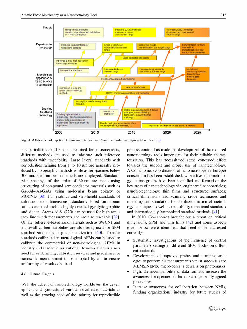
Fig. 4 iMERA Roadmap for Dimensional Micro- and Nano-technologies. Figure taken from [43]
Atomic Force Microscopy as a Nanometrology Tool 317
123
probe-sample interaction as the key to progress in this
field
The iMERA roadmap [43] was developed by represen-
tatives of a delegation of European Metrologists Institutes
(EUROMET) which projects the needs for Nanometrology
for the future (see Fig. 4). Accordingly, some targets have
been laid out for the coming 10–12 years (until 2025). The
target for the next 5 years (up to 2018), is development of
‘Traceable 2D (3D) metrology with sub-nm accuracy over
sample measurement ranges of sub-mm range’, which is to
be further extended to sample measurement ranges of about
100 mm range by 2025. In order to meet these challenging
targets, efforts are needed for evolving instrumentation for
2D (3D) positioning systems with nm-level accuracy over
sub-mm range which will require high precision displace-
ment interferometry. Refined optical interferometry and
X-ray interferometry have been suggested as possible routes
to achieve this. The design of new types of probes which
would be capable of fast sensing and resistant to wear and
tear will be required. The study of the interaction forces
between the probe and surface depending upon the material
and dimension, using modeling and simulation, has been
identified as one important research area. To calibrate the
newly developed instrumentation, various nanostandards
over sum-mm to 100 s of mm will be required. This will
need development of novel nanofabrication techniques.
From the point of view of metrology and required trace-
ability, various measurement parameters will need to be
correlated. Hence, traceable single-probe 2D (3D) instru-
mentation will need to be evolved to multi-probe 2D (3D)
instrumentation. In addition, calibration techniques, strate-
gies and guidelines for nanoscale measurements will need to
be provided to standardize the measurement results.
5. Conclusion
Certain general aspects of AFM design that require further
development would be to make AFM system less sensitive
to mechanical, thermal and environmental factors. To
achieve the targets set forth by the European Metrology
Institutes, AFM instruments with large measurement range
together with high-speed measurement capabilities will
need to be developed, which would be especially relevant
in certain fields like surface science and biological science.
A multi-probe instrumentation by combining SEM, TEM,
Optical profiler and confocal laser scanning microscopy
and others will help towards verification of measurement
results using different techniques. A set of measurement
strategies in the contact mode and non-contact AFM modes
for different samples need to be established and made
available in the form of reference data as well as some
commonly adopted guidelines for calibration of the
instrument need to be set up, in order to bring uniformity in
the interpretation of AFM measurement results all across.
Advancement in the theoretical and simulation studies of
probe-sample interaction forces will be important for the
progress in the field of accurate quantitative determination
of intermolecular forces using AFM.
References
[1] G. Binnig, H. Rohrer, C. Gerber and E. Weibel, Surface studies
by scanning tunnelling microscopy, Phys. Rev. Lett., 49 (1982)
57–61.
[2] G. Binnig, C.F. Quate and C. Gerber, Atomic force microscope,
Phys. Rev. Lett., 56 (1986) 930–933.
[3] F.J. Giessibl, Atomic force microscopy in ultrahigh vacuum,
Jpn. J. Appl. Phys., 33 (1994) 3726–3734.
[4] F.J. Giessibl, Advances in atomic force microscopy, Rev. Mod.
Phys., 75 (2003) 949–983.
[5] Y. Song, A.F. Otte, V. Shvarts, Z. Zhao, Y. Kuk, S.R. Blan-
kenship, A. Band, F.M. Hess and J.A. Stroscio, Invited review
article: a 10 mK scanning probe microscopy facility, Rev. Sci.
Instrum., 81 (2011) 121101.
[6] M.R. Koblischka, U. Hartmann, Recent advances in magnetic
force microscopy, Ultramicroscopy, 97 (2003) 103–112.
[7] W. Melitz, J. Shena, A.C. Kummela and S. Lee, Kelvin probe
force microscopy and its application, Surf. Sci. Rep., 66 (2011)
1–27.
[8] R. Garcia, R.V. Martinez and J. Martinez, Nano-chemistry and
scanning probe nanolithographies, Chem. Soc. Rev., 35 (2006)
29–38.
[9] R.D. Piner, J. Zhu, F. Xu, S. Hong and C.A. Mirkin, Science,
283 (1999) 661–663.
[10] X. Li, B. Bhushan, A review of nanoindentation continuous
stiffness measurement technique and its applications, Mater.
Charact., 48 (2002) 11–36.
[11] O. Jusko, X. Zhao, H. Wolff and G. Wilkening, Design and three
dimensional calibration of a measuring scanning tunneling
microscope for metrological applications, Rev. Sci. Instrum., 65(1994) 2514–2518.
[12] V. Korpelainen, J. Seppa and A. Lassila, Design and charac-
terization of MIKES metrological atomic force microscope,
Precis. Eng., 34 (2010) 735–744.
[13] P. Klapetek, M. Valtr and M. Matula, Long range scanning
probe microscope for automotive reflector optical quality
inspection, Meas. Sci. Technol., 22 (2011) 094011.
[14] A. Yacoot and L. Koenders, Aspects of scanning force micro-
scope probes and their effects on dimensional measurement, J.
Phys. D: Appl. Phys., 41 (2008) 103001–103046.
[15] R. Garcıa and R. Perez, Dynamic atomic force microscopy
methods, Surf. Sci. Rep., 47 (2002) 197–301.
[16] F. Ohnesorge and G. Binnig, True atomic resolution by atomic
force miscroscopy through repulsive and attractive forces, Sci-
ence, 260 (1993) 1451–1456.
[17] T. Kizuka and K. Hosoki, In situ high-resolution transmission
electron microscopy of direct bonding processes between silicon
tips with oxide surface at room temperature, Appl. Phys. Lett.,
75 (1999) 2743–2745.
[18] S. Kasas, G. Longo and G. Dietler, Mechanical properties of
biological specimens explored by atomic force microscopy, J.
Phys. D, 46 (2013) 133001–133013.
318 G. Raina
123

[19] Z.L. Zhou, A.H.W. Ngan, B. Tang and A.X. Wang, Reliable
measurement of elastic modulus of cells by nanoindentation in
an atomic force microscope, J. Mech. Behav. Biomed. Mater., 8(2012) 134–142.
[20] J.E. Griffith, Dimensional metrology with scanning probe
microscopes, J. Appl. Phys., 74 (1993) R83–R10.
[21] E. Manske, G. Jager, T. Hausotte and R. Fubl, Recent devel-
opments and challenges of nanopositioning and nanomeasuring
technology, Meas. Sci. Technol., 23 (2012) 74001–74010.
[22] X. Hu, C.J. Tourek, Z. Ye, S. Sundararajan and A. Martini,
Structural and chemical evolution of the near-apex region of an
atomic force microscope tip subject to sliding, Tribol. Lett. DOI
10.1007/s11249-013-0255-2, 2013.
[23] M.-S. Kim, J.-H. Choi, J.-H. Kim and Y.-K. Park, Accurate
determination of spring constant of atomic force microscope
cantilevers and comparison with other methods, Measurement,
43 (2010) 520–526.
[24] F. Zenhausern, M. Adrian, B.T. Heggler-Bordied, L.M. Eng and
P.D. Descouts, DNA and RNA-polymerase DNA complex
imaged by scanning force microscopy—influence of molecular-
scale friction, Scanning, 14 (1992) 212–217.
[25] V.J. Garcıa, L. Martinez, J.M. Briceno-Valeron and C.H.
Schilling, Dimensional metrology of nanometric spherical par-
ticles using AFM: II, Probe Microsc., 1 (1998) 117–125.
[26] Y. Wang and X. Chen, Carbon nanotubes: a promising start for
quantitative evaluation of AFM tip apex geometry, Ultrami-
croscopy, 107 (2007) 293–298.
[27] J.S. Villarrubia, Algorithms for scanned probe microscope
image simulation, surface reconstruction and tip estimation, J.
Res. Natl. Inst. Stand. Technol., 102 (1997) 245–254.
[28] D. Tranchida, S. Piccarlo and R.A.C. Deblieck, Some experi-
mental issues of AFM tip blind estimation: the effects of noise
and resolution, Meas. Sci. Technol., 17 (2006) 2630–2636.
[29] C.A.J. Putman, B.G. de Grooth, N. van Hulst and G.J. Greve, A
theoretical comparison between interferometric and optical beam
deflection technique for the measurement of cantilever displace-
ment in AFM, Ultramicroscopy, 42–44 (1992) 1509–1513.
[30] T. Fukuma, M. Kimura, K. Kobayashi, M. Kazumi and H. Ya-
madaa Development of low noise cantilever deflection sensor
for multi environment frequency-modulation atomic force
microscopy, Rev. Sci. Instrum., 76 (2005) 53704–53711.
[31] M. Tortonese, R.C. Barrett and C.F. Quate, Atomic resolution
with an atomic force microscope using piezoresistive detection,
Appl. Phys. Lett., 62 (1993) 834–836.
[32] J.A. Harley, Ph.D. Thesis, Advances in piezoresistive probes for
atomic force microscopy, (Guided by C.F. Quate), Stanford
Univ, Mar (2000).
[33] G.E. Fantner, D.J. Burns, A.M. Belcher, I.W. Rangelow, K.
Youcef-Toumi, DMCMN: in depth characterization and control
of AFM cantilevers with integrated sensing and actuation, J.
Dyn. Syst. Meas. Control, 131 (2009) 61104–61111.
[34] K. Dransfeld, P. Guethner and K. Heitmann, US Patent 5, 212,
987, US Patent and Trademark Office (1993).
[35] H. Edwards, L. Taylor, W. Duncan and A.J. Melmed, Fast, high-
resolution atomic force microscopy using a quartz tuning fork as
actuator and sensor, J. Appl. Phys., 82 (1997) 980–984.
[36] F.J. Giessibl, F. Pielmeier, T. Eguchi, T. An and Y. Hasegawa,
Comparison of force sensors for atomic force microscopy based
on quartz tuning forks and length-extensional resonators, Phys.
Rev. B, 84 (2011) 125409–125424.
[37] List of reference standards, http://www.nanoscale.de/standards.
Accessed 26 Sept 2013.
[38] L. Koenders, T. Dziomba, P. Thomsen-Schmidt, and G. Wilk-
ening, Standards for the calibration of instrumentsfor dimen-
sional nanometrology, in Nanoscale calibration standards and
methods dimensional and related measurements in the micro-
and nanometer range, ed. by G. Wilkening and L. Koenders,
Wiley, Weinheim (2005) pp. 245–258.
[39] B. Andreas et al., Determination of the Avogadro constant by
counting atoms in a 28Si crystal, Phys. Rev. Lett., 106 (2011)
30801–30804.
[40] D. Fujita, K. Onishi and M. Xu, Standardization of nanomate-
rials characterization by scanning probe microscopy for societal
acceptance, J. Phys: Conf. Ser., 159 (2009) 12002–12006.
[41] EU project Co-Nanomet, http://www.co-nanomet.eu. Accessed
26 Sept 2013.
[42] H.U. Danzebrink and L. Koenders, Co-nanomet workshop on
critical dimensions and scanning probe techniques & thin films,
Brno, Oct 2010.
[43] iMERA Roadmaps, http://technologyroadmaps.eu/doku.php?id=
micro_and_nano. Accessed 14 Sept 2013.
Atomic Force Microscopy as a Nanometrology Tool 319
123