Review of current progress in nanometrology with the ...
15
Review of current progress in nanometrology with the helium ion microscope This article has been downloaded from IOPscience. Please scroll down to see the full text article. 2011 Meas. Sci. Technol. 22 024004 (http://iopscience.iop.org/0957-0233/22/2/024004) Download details: IP Address: 129.6.97.37 The article was downloaded on 05/01/2011 at 18:31 Please note that terms and conditions apply. View the table of contents for this issue, or go to the journal homepage for more Home Search Collections Journals About Contact us My IOPscience
Transcript of Review of current progress in nanometrology with the ...

Review of current progress in nanometrology with the helium ion microscope
This article has been downloaded from IOPscience. Please scroll down to see the full text article.
2011 Meas. Sci. Technol. 22 024004
(http://iopscience.iop.org/0957-0233/22/2/024004)
Download details:
IP Address: 129.6.97.37
The article was downloaded on 05/01/2011 at 18:31
Please note that terms and conditions apply.
View the table of contents for this issue, or go to the journal homepage for more
Home Search Collections Journals About Contact us My IOPscience

IOP PUBLISHING MEASUREMENT SCIENCE AND TECHNOLOGY
Meas. Sci. Technol. 22 (2011) 024004 (14pp) doi:10.1088/0957-0233/22/2/024004
Review of current progress innanometrology with the helium ionmicroscopeMichael T Postek1,3, Andras Vladar1, Charles Archie2 and Bin Ming1
1 National Institute of Standards and Technology4,5, Gaithersburg, MD 20899, USA2 IBM, Semiconductor Research and Development Center, Systems and Technology Group,Hopewell Junction, NY 12533, USA
E-mail: [email protected]
Received 11 April 2010, in final form 8 July 2010Published 21 December 2010Online at stacks.iop.org/MST/22/024004
AbstractScanning electron microscopy has been employed as an imaging and measurement tool formore than 50 years and it continues as a primary tool in many research and manufacturingfacilities across the world. A new challenger to this work is the helium ion microscope (HIM).The HIM is a new imaging and metrology technology. Essentially, substitution of the electronsource with a helium ion source yields a tool visually similar in function to the scanningelectron microscope, but very different in the fundamental imaging and measurement process.The imaged and measured signal originates differently than in the scanning electronmicroscope and that fact and its single atom source diameter may be able to push theobtainable resolution lower, provide greater depth-of-field and ultimately improve themetrology. Successful imaging and metrology with this instrument entails understanding andmodeling of new ion beam/specimen interaction physics. As a new methodology, HIM isbeginning to show promise and the abundance of potentially advantageous applications fornanometrology has yet to be fully exploited. This paper discusses some of the progress madeat NIST in collaboration with IBM to understand the science behind this new technology.
Keywords: helium ion, microscope, HIM, scanning electron microscope, SEM,nanomanufacturing, nanometrology, critical dimension
1. Introduction
Nanotechnology and the associated nanometrology arepushing current technology to its limits [1–4]. Thescanning and transmission electron microscopes haveincrementally improved in performance and other scannedprobe technologies such as atomic force microscopy, scanningtunneling microscopy and focused ion beam microscopy haveall been applied to nanotechnology with various levels of
3 Author to whom any correspondence should be addressed.4 Contribution of the National Institute of Standards and Technology, notsubject to copyright.5 Certain commercial equipment is identified in this report to adequatelydescribe the experimental procedure. Such identification does not implyrecommendation or endorsement by the National Institute of Standards andTechnology, nor does it imply that the equipment identified is necessarily thebest available for the purpose.
success. Over the years, the evolution of these technologieshas been steady and highly responsive to the needs of theresearch community.
A new tool for nanotechnology is the scanning heliumion microscope (HIM). As reported in earlier papers [5–10],the HIM is a new approach to imaging and metrology fornanotechnology which may be able to push the currentresolution barrier lower and provide new contrast mechanisms(figure 1). This means that the metrology done withthis instrument can be better for some materials than forits electron beam instrument counterparts. The HIM alsopromises the potential for greater depth of field (DOF), newimaging modes and the potential for charge-free imagingat higher landing energies without the need for conductivecoating. But, successful imaging and metrology with thisinstrument entails development of new ion beam/specimen
0957-0233/11/024004+14$33.00 1 © 2011 IOP Publishing Ltd Printed in the UK & the USA

Meas. Sci. Technol. 22 (2011) 024004 M T Postek et al
Figure 1. Resolution and depth of field in the helium ion microscope. (Left) 60 nm gold particles (field of view = 1000 nm) and (right)evaporated nickel particles (field of view = 2.5 μm).
interaction physics which is different from the current electronbeam interaction models. As a new methodology, HIM isbeginning to show promise and the abundance of potentiallyadvantageous applications for nanometrology has yet to befully exploited.
The National Institute of Standards and Technology(NIST) was fortunate to receive the first commercial HIM[6] and this paper discusses some of the progress made atNIST in collaboration with the IBM Semiconductor Researchand Development Center to improve its performance andto understand the science and capabilities of this newinstrumentation for dimensional metrology. In addition, itis the NIST goal to understand potential differences betweenHIM and contemporary scanning electron microscope (SEM)instruments. Clearly, this is a difficult task since the SEMand the HIM appear similar in that both are scanned particlebeam instruments but are quite different in their evolutionarystate, operational parameters, modeling and state of metrologydevelopment.
2. Materials and methods
2.1. Instruments
The scanning helium ion microscopes used in this workwere either a Zeiss Orion Plus HIM installed in theNIST Advanced Measurement Laboratory or an engineeringinstrument installed at the Zeiss/ALIS (see footnote 5) facilityin Peabody, MA.
2.2. Sample preparation
No special sample preparation techniques were used forgeneral imaging and metrology. HIM sample preparationis generally similar to that used for standard SEM samplepreparation.
Figure 2. Test structures used in the photoresist studies. (Left)computer aided design of the test structures. (Right) SEM image ofthe patterned photoresist structures (field of view = 3 μm). Thisoverall pattern is designed for cross section metrology (as describedin the text). The nested lines extend for several millimeters on thewafer in order to facilitate cleaving the wafer through the lines.
2.3. Experiments on photoresist patterned silicon wafers
One photoresist system was exposed using a 248 nm deepultraviolet (DUV) lithography process, while the other useda 193 nm process. Both were chemically amplified resistsystems where the total exposure energy dose came from acombination of the photon exposure and a subsequent timedbake at elevated temperature. Both resist systems are known tobe affected by modest irradiation, such as that caused by SEMimaging. The same photomask was used for both exposures.Figure 2 (left) shows the computer aided design of the teststructure used in the studies and figure 2 (right) is a SEM imageof the actual patterned photoresist structures (left). Thesestructures are designed for cross section metrology; the nestedlines extend for several millimeters on the wafer in order tofacilitate cleaving the wafer through the lines. Diagonal breaksin the lines occur every 5 μm. The linewidth is approximately
2

Meas. Sci. Technol. 22 (2011) 024004 M T Postek et al
Figure 3. DOF and the effect of beam defocus on imaging and metrology. (Left) beam focused on substrate. The 3D conical electron beam,scanning from left to right, interacts with the leading edge of the structure prior to the focal point. Thus, the signal from the leading edge issummed with the signal from the location of the primary beam interaction. (Right) beam focused on the top of the sample. As the focusedbeam leaves the sample it is defocused at the substrate. The larger the DOF characteristic of the instrument, the less the impact of thisproblem.
135 nm. The structures on the wafer offer many similarlocations for experimentation. After construction of the wafersand survey by SEM to confirm print quality, the waferswere diced to produce wafer fragments of less than 3 cm2
which are suitable for insertion into the HIM. Some fragmentscontained complete versions of the design while others wereintentionally cleaved to bisect the structures in order to studyin the cross section mode. These experiments were conductedat the Zeiss/ALIS factory in Peabody, MA. The HIM used a31.5 keV beam with a 10 pA probe current. The HIM usesa mechanical cryocooler to reduce the temperature of the gundown to 72–74 K. During actual scanning, this cooling devicewas turned off in order to reduce vibrations.
3. Comparison of the scanning electron and heliumion microscopes
3.1. The primary electron and ion beams
The scanning electron microscope and the helium ionmicroscope share a number of fundamental characteristics.The primary beam in each microscope is composed of athree-dimensional distribution of electrons or ions along andacross the beam. The beam is generally thought to have asomewhat double-conical shape. This defines the importanthalf-angle parameter that determines the DOF and the diskof least confusion where the best focus (i.e. the smallestspot size) can be achieved. The small beam convergenceangle of the particle beam instruments results in high DOF.Large DOF has always been a positive characteristic of thescanning electron microscope [11], but it can be even morepronounced in the HIM. This is a consequence of the singleatom source of the ions with the HIM [12–15]. Under normaloperating conditions, this can result in a narrower convergenceangle than the SEM (depending upon the instrument operatingconditions). Therefore, the overall DOF can be larger thanthe SEM even at higher magnifications [15]. In certain cases,using the most optimum conditions and instrument settings,the DOF of the HIM can be as much as five times greater thanthe SEM.
Large DOF is highly desirable. The size of the DOFcan have consequences to the metrology with scanned beamsystems especially where high-aspect ratio structures areconcerned. This relates directly to whether the beam is focusedon the top of a structure or the base of the structure and thenbecomes an important measurement consideration (figure 3).When the particle beam is focused at the substrate, signal maybe generated by the beam remotely from the smallest focalspot because a portion of the beam above the surface contactsthe structure before the focused part of the beam scans to it(figure 3, left). Conversely, if the beam is focused at the topof a structure (figure 3, right), it will rapidly defocus whenit reaches an edge and then be somewhat defocused at thesubstrate. The larger the DOF, the less this affects the imagingand metrology.
3.2. Excited volume
One of the key issues for nanometrology in any particle beaminstrument is the understanding that signal is generated frommore than just the initial point of impact of the primary beam.The ‘image’ is a point-by-point representation of the totalsignal generated as the beam is scanned across a given sample.Any modification of that signal due to signal generation orcollection inefficiency will be mirrored in the imaged ormeasured data.
Depending upon the particle source, accelerating voltageand materials irradiated, there is a finite volume excited by theprimary particle beam. This volume may extend quite deeplyinto the material. Ideally, the beam would only interact withthe surface, but that is not the case. The current understandingis that the volume excited by the primary electron beamin the SEM and the volume excited by the HIM are quitedifferent [6]. Figure 4 illustrates a comparison of modeledelectron beam interaction data from the Monte Carlo programCASINO 2.42 [16–18] (left) and ion beam interaction datamodeled by SRIM 2008.04 [19] (right). In both of themodeled examples, 30 keV particles are interacting with aninfinitely thick silicon (Si) sample. Note the fundamental
3

Meas. Sci. Technol. 22 (2011) 024004 M T Postek et al
Figure 4. Comparison of the electron beam interaction data from the Monte Carlo program CASINO 2.42 (left) and ion beam interactiondata modeled by SRIM 2008.04 (right). In both of the modeled examples, 30 keV particles are interacting with an infinitely thick siliconsample. Note the fundamental difference in the size and depth of the interaction volumes, especially in the top figures.
difference in the interaction volumes especially in the lowercomparison. This volume is where the important beam–specimen interactions take place and it has been modeled,as well as, documented experimentally for the SEM [20, 21]but has not been done, as of yet, for the HIM.
Within the excited volume, the secondary electron (SE)escape depth is that region from which the SEs have enoughenergy to leave the sample surface to be potentially collected.The deeper the SE are generated, the less likely they will escapeand be collected. Typically, the escape depth can be a fewnanometers to up to more than 10 nm, depending on the samplematerial. For metals, the depth is shallower; for insulators andbiological materials, it is generally larger. The shape and size,the depth reached by electrons and ions and the SE generationefficiency all strongly depend on the landing energy of theelectrons or ions and the sample material irradiated. Thelanding energy of electrons in an SEM is variable; however,adjustable ion acceleration in the HIM is a capability still tobe implemented in the NIST HIM (this capability will greatlyexpand the parameter space for all HIM experiments).
It is clear from model shown in figure 4 (lower) that as theion beam enters the sample, it scatters far less within the SEescape zone than electrons. The positive consequence of thisis that fewer SEs are generated near the surface or remotelyfrom the impact point of the primary ion beam (figure 5). Infigure 5, one can readily see that in the SEM, signal can begenerated from regions quite a distance from the incidentprimary beam not just that single point where the primarybeam enters the sample. All of the sources of the signal aresummed for each pixel of the image collected. Hence, (asdiscussed below) the SE signal can be recorded from areasof the sample remote from the impact point of the primarybeam.
The ion scatter characteristic of the HIM, described above,can also be exploited for extremely fine line lithography.Electron beam lithography (EBL) has been used in lithographicpatterning for many years. EBL suffers from many of thesame issues as SE imaging such as extraneous exposurefrom fast SEs and backscattered electrons. Focused ionbeam lithography with a gallium source has not been
4

Meas. Sci. Technol. 22 (2011) 024004 M T Postek et al
Figure 5. Diagrammatic representation of the contemporary understanding of the difference between the signal generating interactions inthe SEM (left) and the HIM (right).
used extensively for resist patterning mainly because ofthe resolution constraints. However, HIM lithography with∼200 nm resolution was demonstrated over 20 years ago, butit suffered from a lack of adequate ion column technology tomake it a viable competition to EBL [22]. One advantageto using helium ions for lithography is the potential forhigher resolution lithography than electrons. The helium ionmicroscope has demonstrated that it is capable of generatingextremely fine lines with extremely straight walls due to thedeep penetration of the helium ions into the substrate andthe lack of additional secondary exposure mechanisms whichcan degrade the lithographic fidelity. Winston et al [23]has shown dense arrays of approximately 15 nm diameterhydrogen silsesquioxane (HSQ) resist posts generated byhelium ion lithography. HSQ is a high resolution electronbeam resist and it permits high-resolution SEM inspectionfollowing patterning and development. The helium ion beamlithography technology is in its infancy but, it has alreadydemonstrated an ability to fabricate less than 10 nm lineswith a 20 nm pitch [23]. There is still much to be done,but ion beam lithography shows promise and the sensitivityof the resist materials can be substantially higher, so higherthroughput lithography may be possible.
3.3. Enhanced surface detail
In both the SEM and HIM the size and shape of the excited andinformation volumes along with the SE generation efficiencyand location are important for another reason. The amount ofsurface-related information collected is directly dependent onthese factors. Those SE carrying information about the finestdetails of the sample are generated by the primary electronsor ions at the point where the beam hits the sample. Theseare the so-called SE-1 type electrons. The SEs that werecreated by energetic electrons or ions backscattered withinthe sample are designated as SE-2 electrons. Because of thelocation of their generation in the SEM, the SE-2 do not carryinformation about finest sample details; in fact, it is clearlyshown in figure 5 (left) that current modeling shows that manymore electrons emerge remotely from the initial point of the
primary electron interaction than shown in the modeled datafrom the ion beam. The consequence of this is a reduction ofcontrast of the fine structure. The size of this area depends onthe primary excitation and the material composing the sampleunder examination and can extend more than a micrometerin diameter [24]. Electrons can also be generated by thebackscattered electrons or ions that leave the sample and hitsome other material within the sample chamber or the sampleitself. These SEs are called SE-3. Again, these do not carryinformation about finest sample details. What is not shown infigures 4 and 5 is the additional cascade of SEs generated bythese interactions which may magnify this by a factor of 3 to5 times.
The well-focused beam always generates SE-1, but therelative amounts of SE-1, SE-2 and SE-3 electrons generatedin total have a profound effect on the appearance and theamount of fine details resolved in the SE image. Peters [25]measured the individual contributions of the components ofthe SE signal (in the SEM) from gold crystals and foundthat, depending upon the sample viewed, for the total SEimage, the contribution of the SE-2 is approximately 30%and the contribution to the image of the SE-3 electrons isapproximately 60% as compared with approximately 10%of the image contributed by the SE-1 derived signal. Thisratio of SE-2/SE-1 generated by electrons significantly reducesthe contrast and resolvability of small features. Clearly, thisdepends on landing energy, the SE and backscattered electronor ion yields.
In the HIM, SEs forming the image are produced at (orvery near) the point of initial interaction with the sample, andthus are equivalent to SE-1 electrons of the SEM (figure 5).The initial SEs produce images with strong and topographiccontrast, and generally appear very similar to the SE imagesobtained from an SEM, upon first inspection. IONiSEmodeling [26, 27] predicts that the helium-ion-generated SE-2/SE-1 ratio should be lower than that for electron irradiationespecially at the higher landing energies. Hence, the contrastand the surface details are enhanced. In contrast to theSEM interactions, the ion beam passes much more deeplyinto the sample matrix (figure 5) and very few SE-2 or SE-3 type electrons that can dominate in the SEM imaging are
5

Meas. Sci. Technol. 22 (2011) 024004 M T Postek et al
Figure 6. HIM imaging and surface structure enhancement. (Left) typical gold-on-carbon image test sample viewed in the HIM (field ofview = 1.5 μm). Note that surface detail is being resolved on the top surface of the gold islands which would not be typically observed in asimilar SEM image. (Right) carbon nanotube material with tin and palladium nanoparticles on or near the surface (field of view = 500 nm).
generated. The flood of SE-2 and SE-3 electrons resultingfrom the backscatter of electrons in the SEM can essentially‘wash-out’ some of the surface detail potentially resolved bythe electron beam. This does not occur to the same extent inthe HIM, resulting in the enhanced surface detail as shownin figure 6. Thus, in a material infinitely thicker than the SEescape depth, clear surface detail may be resolved.
A flat sample is instructive, but dimensional metrology isthe measurement of a structure of some sort. Structures haveedges and we usually make measurements from one ‘edge’ toanother edge such as the diameter of a gold particle, or thecritical dimension of a semiconductor device gate. Edges arealso found at grain boundaries and material interfaces. If anedge is introduced at the point of primary beam incidence,depending upon the angle selected, the collected signal canbe generated from points down the slope of that structurewhere the excited volume approaches the surface. All signalsgenerated are summed for that particular pixel. This explainsthe bright edges on the typical SEM image. For accuratemetrology, understanding all of the interactions involved inthe signal generation process is extremely important in orderto obtain meaningful dimensional information because the sizeof the edge ‘bloom’ in the SEM is often larger than the desiredmeasurement accuracy.
Due, in part, to the huge difference between the electronand ion interaction volume and the reduction of SE-2, andSE-3 electrons, it is clear that a fundamental difference in thesignal-to-noise ratio between the SEM and the HIM is possible.Peters demonstrated that up to 90% of the collected SEMsignal is composed of electrons generated remotely from theinitial impact of the primary electron beam [25]. Hasselbachand Mollenstedt [24] also showed experimentally using theemission microscope that the collected signal from the SEMcould be generated from adjacent structures micrometersfrom the primary beam impact point. In comparison, in
the HIM, the collection of the equivalent of SE-2 and SE-3signals is greatly minimized because their signal contributionis formed too deeply in the material for them to escape. Edgeenhancement in the HIM still occurs, but is a function ofthe structure size relative to the ion beam penetration andscatter. Hence, the main contributors to the total HIM imageare the SE-1 electrons. It stands to reason that in the HIM, theamount of signal collected under similar conditions to the SEMshould differ, as well as the contrast of the surface structure.Measurement of these differences is an area of research at thecurrent time, and as more is known these thoughts may berefined. But, what is clear is that fine detail on the surface of asample such as in figure 6 (left) will appear more readily in theHIM since the other signal mechanisms potentially ‘washing-out’ the fine detail in the SEM are minimized.
Sub-surface contributions to the SEM image are commonand can also be found in the HIM image. In very thinmaterials, low in atomic number or those that are flocculent,significant contributions to the image can be made fromunderlying structures (figure 6 right). The SEM or HIM beamenters the first layer of the sample, generates signal and thenpasses through (potentially generating signal as well). As itstrikes another adjacent fiber or portion of the sample, it alsogenerates signal [11]. The sum of both is collected by theSE detector. This effect can be seen on some of the carbonnanotubes in figure 6 (right) where a sub-surface ‘ghosting’occurs. Other possible mechanisms for generating the sub-surface signal in bulk samples include electron channelingeffects. Further research into these mechanisms and theunderlying physics needs to be done in order to understandfully these observations. For now, adjusting instrumentoperating conditions helps to minimize these contributions.
Modeling is an excellent tool for understanding thephysics of electron and ion interactions. NIST has devoteda great deal of effort to modeling and has a long history
6

Meas. Sci. Technol. 22 (2011) 024004 M T Postek et al
Figure 7. Imaging of uncoated chromium on glass photomasks by incorporating the electron flood gun to eliminate positive chargebuild-up. (Field of view = 700 nm, left; 500 nm, right.)
in this area. The most recent improvements in the NISTprogram JMONSEL are documented by Villarrubia et al[28, 29]. Villarrubia et al (2007) detail how 3D shapesare described and how a scattering calculation is made [28].Villarrubia et al (2009) describe subsequent improvements tothe physics model and the relationship between the models oneuses and the resulting measurement values (e.g., for positionsof a feature’s edges) [29].
3.4. Signal collection
Measurements made in particle beam instruments aremade from the collected signal chosen (secondary electron,backscattered electron, transmitted electron, etc). It must beunderstood that the signal measured is a complex product of(a) the interaction of the electron or ion probe with the sample,(b) the composition of the sample, (c) the sample chambergeometry and chamber material, (d) the type of detector used,and (e) the electro-magnetic fields present around the sample(either from the instrument itself or from sample biasingand/or charging). Where the critical dimension metrologySEM (CD-SEM) is concerned many of these parameters arefixed, and nearly ‘identical’ samples are viewed on a day-by-day basis. Because of this tight control, a very highdegree of precision can be obtained. However, accuracyis a different issue [30]. Sophisticated modeling methodsthat account for all the physical processes must be used tomeasure accurately the shape and size of the sample structuresof interest [13]. Monte Carlo models have been in use atNIST to deconvolute the edge information from the collectedsignal, and those models are being modified to accommodatethe signal generated in the HIM. Work is ongoing to combinethe physics of the IONiSE Monte Carlo model [26, 27]with the 3D shape modeling of JMONSEL [28, 29] and will aidin the prediction of topographic yield variation of the heliumgenerated SE as a function of the sample composition andstructure shape. With this model, the important details of
helium ion SE imaging can be compared with comparableelectron-generated SE imaging. Such work is an importantand primary step in the understanding of the imaging andmetrology of the HIM.
3.5. Charge reduction
Current HIM instruments operate routinely at highaccelerating voltages. Many samples being viewed can buildup a positive charge on the surface. Unlike the SEM,where the negative charge build-up can be quite high, highenough to detrimentally deflect the electron beam in someinstances, the positive charging in the HIM can be eliminatedor at least minimized by employing an electron flood gun.Operating conditions can be established to facilitate viewingnonconducting materials such as photoresist or biologicalsamples.
The electron flood gun is also useful in imaging andmetrology of insulating materials such as chromium on quartzphotomasks. Photomasks can be very difficult to image in theSEM due to charge build-up in the quartz. Postek et al (2003)successfully used variable pressure SEM to dissipate thecharge build-up for the imaging and metrology of chromiumphotomasks [31]. The HIM can also be successfully employedin the imaging and metrology of these samples (figure 7).The positive charge build-up was removed by employing anelectron flood gun, thus enabling high resolution imagingof the chromium photomasks. Optimization of the electronflood gun is currently being undertaken to determine theproper conditions for common semiconductor materials andthe effects of this tool upon measurements (such as beamdeflection) made while it is being operated.
3.6. Helium ions
Current theory is that most of the He ions remain embedded inthe sample due to the low backscattered ion coefficient for He.
7

Meas. Sci. Technol. 22 (2011) 024004 M T Postek et al
Figure 8. Comparison of SEM and HIM. (Left) typical SEM and HIM images of polysilicon structures (field of view of 3 μm). Note thedifference in contrast and edge definition. (Right) comparison of linescans of conductive patterned amorphous silicon lines and thecomplementary SEM (upper line) and HIM images (lower line) exhibiting similar characteristics.
The ions may cause swelling, formation of tiny bubbles, andin certain cases diffuse out of the sample. For many practicalcases and primary ion currents, the effects of the embeddedHe ions are negligible, and do not prevent high-resolutionimaging. The images in this and other publications attest tothis. The effect of the He ions on sensitive samples is currentlybeing researched.
4. Semiconductor imaging and metrology
The potential of achieving higher resolution and greatersurface sensitivity has prompted a great deal of interest inthe HIM for semiconductor metrology applications. The SEMis currently the tool of choice for semiconductor production,and sample charging is often an issue. Many samples inthe SEM are prone to charging, and charge reduction iscommonly achieved by lowering the accelerating voltage downinto the 1 kV range to achieve a charge balance [32]. Theimmediate result has, historically been, a significant reductionin resolution due to beam broadening. Hence, edge definitionis also broadened. Modeling has been able to deconvoluteedge information from the images, but requires an accuratemodel to be used in conjunction with a well-characterizedinstrument. Aberration corrected SEMs working at lowaccelerating voltage may, in the near future, improve uponthis situation and this avenue is also being explored currently.
Semiconductor metrology with the HIM is different(today) in that most of the commercial HIMs operate at highelectron landing energies, and a variable accelerating voltageoption is just being implemented in on these instruments inthe field. Therefore, no quantitative comparisons of the HIMand the SEM at a low landing energy have been published.Figure 8 shows a comparison of linescans of conductivepatterned amorphous silicon lines. These are complementarySEM (figure 8, upper) and HIM images (figure 8, lower).The images (and linescans) were both taken at high landing
energies and thus provides highly distinct edge definition asshown in the figure. But, note that the contrast range in theHIM image is much greater. Thus, allowing more flexibilityin the measurement algorithm selection and the number ofdata points used in the measurement. In addition, the edgesharpness would be expected to be much higher than that of thelow accelerating voltage SEM. Additional work to understandthe proper conditions for semiconductor metrology with theHIM is ongoing.
The HIM benefits from the difference in specimeninteraction to provide higher surface detail. Modeling ofthe ion beam interaction has shown that in the helium ionmicroscope, the general characteristics of the measurementprofile are similar to those obtained from the SEM. Earlierwork on x-ray mask structures [33] in the SEM withtransmission electron detection demonstrated for the first timea ‘notch’ structure apparent in the modeled linescan. Thisnotch is a consequence of the electron beam generating signalas it scans along the sidewall. The finer the beam and betterthe resolution, the more distinct is the notch. More recentmodeling has shown this to be a characteristic of the SEMsignal generation and now the HIM. Similarly, the modelingmay relate to the time that the ion beam resides on thesidewall of the structure under test. But, since the HIM ispotentially higher in resolution, this characteristic may be morepronounced. The inflection point is thought to be reproducibleand as such is being closely looked at as a possible fiducial tothe location of the structure edge. This may ultimately lead toan accurate measurement even without the benefit of modelingbut with some degree of measurement uncertainty still to bedetermined. Currently, work in this area is also being pursued.
4.1. HIM for semiconductor production applications
As stated above, the HIM is being considered for online andoff-line metrology applications. Hence, a series of preliminarystudies were done to to assess the potential of this technology
8

Meas. Sci. Technol. 22 (2011) 024004 M T Postek et al
Figure 9. Series of HIM slow scan image showing the progression in image quality by differing only the pixel dwell time, as described inthe text. (Top, left) 0.5 μs; (top, right) 2.0 μs; (middle, left) 5.0 μs; (middle, right) 10.0 μs; (bottom, left) 20.0 μs; (bottom, right) 40.0 μs.Note the improvement in the signal-to-noise ratio, but the slimming of the lines in the longer dwell times and the poorer signal-to-noise ratioin the shorter dwell times (field of view = 1 μm).
for these purposes. The work includes (1) the basic imagingconfigurations to assess signal-to-noise conditions, (2) resistdamage section comparing performance of the HIM for twodifferent resist systems currently being used in semiconductorlithography, (3) application of a measure of the apparent beamreporting on a resolution measure that is in common use in thesemiconductor industry [34–37], and (4) an assessment of theHIM for cross section imaging mode.
4.1.1. Imaging for metrology. Patterned photoresiststructures are highly sensitive to electron and ion irradiation,thus it is essential to use the minimum beam exposure dose toaccomplish the metrology task without damaging the material.On the other hand, too few SEs collected per pixel introduceunacceptable shot noise-induced error in the determinationof feature edge location. A compromise between dose andmeasurement signal-to-noise must be achieved. Figure 9shows a series of six slow scan images which differ only inthe pixel dwell time. Dwell times range from 0.5 to 40 μsper pixel. Slow scan imaging refers to capturing the image byperforming a single pass of the beam in raster fashion over the
structure at a rate given by the pixel size divided by the dwelltime. All high magnification imaging in these studies used a1 nm pixel size.
The images in the series show a steady progression inimage quality where the 0.5 μs dwell time image showsspeckling due to low SE count per pixel while the 40 μsimage is remarkably free of this effect. These images werecaptured by scanning only one time at a fresh location atthe stated dwell time. There is a noticeable reduction inlinewidth for the longest dwell times. This effect is referred toas ‘line slimming’. From a metrology perspective the largerdwell times cause too much damage. But, the shorter dwelltimes result in the greater the noise, the greater the potentialmeasurement errors (the next section makes these observationsmore quantitative).
It is appropriate to point out that all particle beaminstruments can induce damage on a sample under test. TheSEM had over 30 years of instrument experience behind itbefore uncoated photoresist samples were routinely viewedin semiconductor production. So, it should be noted that theHIM is a relatively new instrument, so a great deal is still
9

Meas. Sci. Technol. 22 (2011) 024004 M T Postek et al
Figure 10. (Left) graphical analysis showing the full collection of slimming trends from the experiments as discussed in the text. (Right)HIM image showing the line slimming effect due to helium ion exposure (field of view = 2 μm).
to be learned about the proper operating parameters for thesesamples and many others.
4.1.2. Resist damage experiment. To test the effect of thehelium ion beam on patterned photoresist, the basic experimentwas to move and to find a fresh site on the photoresist andacquire ten images using the same imaging conditions foreach data set. Immediately prior to acquiring the ten images,the beam astigmatism was minimized on a nearby structure.Image sets were then acquired for several different dwell timesfor the two resist types. Linewidth measurements of the samecenter line in each image set were performed using a standardcommercial measurement software package [38].
The graphical analysis shown in figure 10 (left) showsthe full collection of the line slimming trends from theexperiments. Closed symbols are 248 nm DUV resist sampleresults and open symbols show 193 nm resist trends. Slimmingtrends for the 193 nm resist system were conducted only at 5and 20 μs dwell times. These trends followed the behaviorseen for the 248 nm resist system. There appears to be anintriguing edge brightening phenomenon that is present inall the image sets but is more pronounced for the higherdwell times; repeated images show systematically brighteredges. The HIM with which this work was done did nothave automatic gain control, so during the first run on the193 nm resist sample for a 20 μs dwell time, the detectoramplifier went into saturation after seven repeats. These beamconditions were then repeated on a fresh site using a loweramplifier gain setting. The two series are shown in the figureand there is excellent reproducibility of the trend up to thepoint of amplifier saturation for the first set. Clearly, all ofthese data show a true slimming trend with helium ion beamexposure.
Additional experiments were conducted using the DUVsamples. They all show that at short dwell time (0.5 μs) theslimming trend is linear with a slope of a few nanometers
per repeat. It is clear, however, that there is scatter of a fewnanometers in the data about the linear trend. This scatter is anindication of the precision of the measurement for these beamconditions. At longer dwell times, the slimming trend is morepronounced and nonlinear. Figure 10 (right) shows a lowermagnification image of the site where the ten 40 μs dwell timeexposures were conducted. Slimming and edge brighteningare clearly evident. The observations suggest that at low dwelltime (0.5 μs or less), modest damage and reasonable precisionis achievable. These data and subsequent experiments haveshown that as the dwell time increases the measured linewidthdecreases. These experiments are another indication that theproper metrology regime needs to be fully researched and shortdwell times are currently recommended.
4.1.3. Apparent beam width. It is clear, from the previousdiscussions, that the term ‘instrument resolution’ is a complexfunction of a number of factors with both the instrumentand sample playing the key roles. The determination of‘resolution’ is more complicated than just laying a ruler ona micrograph and measuring the distance between two points.This concept is more involved than either the classical lightmicroscope or even the TEM. In this instance, the specimenplays a major part in the overall performance measure.Clearly, instrument performance is a major issue and vastimprovements in instrument design have strongly contributedto advances over the years in both SEMs and now theevolution of the HIM. Improved lens designs and illuminationsources have been the main contributors to the increased SEMinstrument performance. But, instrument resolution relies notonly on a high performing instrument design and instrumentoperating conditions, but also on the material being viewedto demonstrate successfully the performance characteristics.Particle beam interactions and also the nature and mannerof the signal being collected are major contributors. Hence,sample choice plays a significant role in demonstrating the
10
Meas. Sci. Technol. 22 (2011) 024004 M T Postek et al
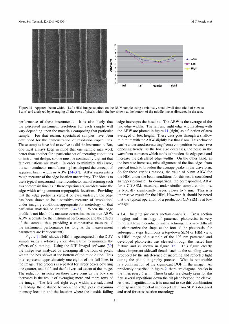
Figure 11. Apparent beam width. (Left) HIM image acquired on the DUV sample using a relatively small dwell time (field of view =1 μm) and analyzed by averaging all the rows of pixels within the box shown at the bottom of the middle line as discussed in the text.
performance of these instruments. It is also likely thatthe perceived instrument resolution for each sample willvary depending upon the materials composing that particularsample. For that reason, specialized samples have beendeveloped for the demonstration of resolution capabilities.These samples have had to evolve as did the instruments. But,one must always keep in mind that one sample may workbetter than another for a particular set of operating conditionsor instrument design, so one must be continually vigilant thatfair evaluations are made. In order to minimize this issue,the semiconductor manufacturing has adopted the concept ofapparent beam width or ABW [34–37]. ABW represents arough measure of the edge location uncertainty. The idea is touse a typical measurand in semiconductor manufacturing suchas a photoresist line (as in these experiments) and determine theedge width using common topographic locations. Providingthat the edge profile is vertical or even undercut, the edgehas been shown to be a sensitive measure of ‘resolution’under imaging conditions appropriate for metrology of thatparticular material or structure [34–37]. When the edgeprofile is not ideal, this measure overestimates the true ABW.ABW accounts for the instrument performance and the effectsof the sample, thus providing a comparative measure ofthe instrument performance (as long as the measurementparameters are kept constant).
Figure 11 (left) shows a HIM image acquired on the DUVsample using a relatively short dwell time to minimize theeffects of slimming. Using the NIH ImageJ software [39]the image was analyzed by averaging all the rows of pixelswithin the box shown at the bottom of the middle line. Thisbox represents approximately one-eighth of the full lines inthe image. The process is repeated for larger boxes coveringone-quarter, one-half, and the full vertical extent of the image.The reduction in noise on these waveforms as the box sizeincreases is the result of averaging more and more rows ofthe image. The left and right edge widths are calculatedby finding the distance between the edge peak maximumintensity location and the location where the outside falling
edge intercepts the baseline. The ABW is the average of thetwo edge widths. The left and right edge widths along withthe ABW are plotted in figure 11 (right) as a function of areaaveraged or box height. These data goes through a shallowminimum with the ABW slightly less than 6 nm. This behaviorcan be understood as resulting from a competition between twoopposing trends: as the box size decreases, the noise in thewaveform increases which tends to broaden the edge peak andincrease the calculated edge widths. On the other hand, asthe box size increases, miss-alignment of the line edges fromvertical tends to broaden the average peaks in the waveform.So for these various reasons, the value of 6 nm ABW forthe HIM under the beam conditions for this test is consideredan upper estimate. In comparison, the corresponding ABWfor a CD-SEM, measured under similar sample conditions,is typically significantly larger, closer to 9 nm. This is aimpressive result for the HIM. However, it should be notedthat the typical operation of a production CD-SEM is at lowvoltage.
4.1.4. Imaging for cross section analysis. Cross sectionimaging and metrology of patterned photoresist is veryimportant to semiconductor manufacturing. It is very difficultto characterize the shape at the foot of the photoresist forsubsequent steps from only a top-down SEM or HIM view.A HIM image of a sample of the 193 nm patterned anddeveloped photoresist was cleaved through the nested linefeature and is shown in figure 12. This figure clearlyshows important sidewall details such as the standing wavesproduced by the interference of incoming and reflected lightduring the photolithography process. What is remarkableis a confirmation of the significant DOF in the image. Aspreviously described in figure 2, there are diagonal breaks inthe lines every 5 μm. These breaks are clearly seen for thefirst several repetitions down the tilt plane beyond the cleave.At these magnifications, it is unusual to see this combinationof crisp near field detail and deep DOF from SEM’s designedand used for cross section metrology.
11

Meas. Sci. Technol. 22 (2011) 024004 M T Postek et al
Figure 12. HIM image of a sample of the 193 nm patterned anddeveloped photoresist cleaved through the nested line featureshowing important sidewall details such as the standing wavesproduced by interference of incoming and reflected light during thelithography process (field of view = 1 μm). Note the significantdepth of field shown in the image.
5. Helium ion beam milling and sample damage
The potential for ion beam-induced sample damage isdiscussed in several sections of this paper. Some level ofchange (‘damage’) in the sample is inevitable during any typeof work with particle beam instrumentation. The point is whattype of changes occur and to what extent. This depends agreat deal upon sample, landing energy and dose, and pre-treatment of the material being imaged or measured and theparticle being used. This varies widely in both the SEM andHIM. Sample damage can be greater in the HIM than the SEMbecause the ions have much higher momentum than electronsof the same energy—and the difference is larger still whenyou take into account that SEM is typically operated at lowerenergy than HIM. It is up to the skilled operator to choosethe optimal setting and imaging conditions to minimize thechange, and for the metrology be able to properly account forit. In some instances the damage is detrimental and should beavoided and in some instances it can be exploited such as fornano-milling.
Depending upon the beam current, the flux of particleswithin the excited volume of either the SEM or the HIM canbe substantial. As shown earlier (section 4.1.2) this current canlead to sample degradation [8]. Moreover, much of the energyof the primary electrons or ions may stay within the sample,which can cause additional adverse effects such as samplemelting, swelling or other dimensional changes. Figure 13is an image showing an example of the potential for highprecision material removal from a sample using the HIM. Thisillustrates the effects of irradiation of approximately 3 pA beamcurrent for approximately 60 s at 28 keV ion landing energyon an evaporated gold island. In figure 13, the instrumentconditions were changed from imaging to a very small scannedregion (very high magnification image setting) for materialremoval. The small square region at the 2 o’clock location hasalso been removed earlier through irradiation with the heliumion beam. In this figure, the small 10 nm hole was intentionallymilled near the center of the gold island in point irradiation
Figure 13. Image of a gold on carbon sample showing the precisionmilling possible with the HIM. A notch was removed from the goldisland as well as a small 10 nm hole milled near the center of theisland (field of view = 800 nm).
mode thus, showing how precisely the beam can be positionedand material removed. The HIM can also be used for moreextensive material removal (or addition) in a similar mannerto the gallium focused ion beam microscope.
5.1. Sample contamination
Electron beam-induced sample contamination is a classicconcern for SEM and HIM imaging and metrology. Thisis another form of specimen damage. Controlling specimencontamination in the SEM has been discussed elsewhere[40, 41] and has direct application to the HIM. The high surfacesensitivity of the HIM (discussed earlier) makes it even moresusceptible to sample contamination than the SEM. This is dueto the effect of the ion beam and the resulting SEs on the thinlayer of molecules of water and carbon dioxide on the sampleor oily residues, either from the stage fabrication process orlubricants. Radio frequency (RF) plasma cleaning [42] hasbeen shown to virtually eliminate sample contamination in theSEM and has been incorporated in the HIM with equal success.
6. Conclusions
A significant and rapid evolution of the HIM instrumentationhas occurred for imaging and metrology. Since itsintroduction, the performance of the instrument has markedlyimproved, as well as the attainable resolution [12, 14].Typically, the benchmark of performance for scanned beaminstruments is the measure of resolution. But, as discussedearlier, resolution determination is more complicated than justlaying a ruler on a micrograph and measuring the distancebetween two points. Shown in this paper has been the
12

Meas. Sci. Technol. 22 (2011) 024004 M T Postek et al
significant part the specimen plays in the overall measurementand hence instrument performance. Clearly, instrumentperformance is a strong issue and vast improvements ininstrument design have strongly contributed to advances overthe years in both SEMs and now the evolution of the HIM.
Research to enable accurate measurements in the HIMis ongoing. This work has documented that the resolutionand DOF of this instrument can be better than the SEM.Equally, this work demonstrates that sample damage is aconcern which must be overcome. Sample ‘slimming’ is aneffect that must be understood and accommodated for bothimaging and metrology. The experiments shown here showthat valuable data can be obtained when this effect is properlyrecognized. Proper conditions for metrology with the HIMmust be developed and this will take a good deal of workto explore the numerous possible operating conditions. Suchwork was needed for the SEM, and over time these conditionswere found and it became a useful ‘tool’ for semiconductormanufacturing. Similar research is needed for the HIM.
Modeling of the HIM signal, just like the SEM signal,is crucial to the measurement capability and much progresshas been made in that area which will ultimately lead toaccurate measurements. However, as demonstrated in thiswork, precise measurements in either the SEM or the HIM canbe accomplished as long as one is careful. As time progressesand more is understood about the imaging mechanisms in theHIM through experimentation and modeling, the advantagesor disadvantages of this new instrument will become moreapparent for nanometrology.
Acknowledgments
The authors would like to thank and acknowledge thecollaboration with D Winston and K Berggren of MIT,Cambridge, MA, on the helium ion beam lithography work andthe strong collaborations afforded by Zeiss SMT, regarding thedevelopment of this paper and their commitment and continuedefforts to improve instrumentation for nanotechnology andnanometrology. They would also like to thank Zeiss forthe use of some of the micrographs used in this paper.The authors would also like to thank both the NIST Officeof Microelectronics Programs and SEMATECH for partiallyfunding this work.
References
[1] Interagency Working Group on Manufacturing 2008 R&DWorkshop Report Instrumentation, Metrology andStandards for Nanomanufacturing available atwww.manufacturing.gov
[2] National Nanotechnology Initiative 2006 NNI GrandChallenge Workshop Report Instrumentation andMetrology available at www.nano.gov
[3] Postek M T and Lyons K 2007 Instrumentation, metrology,and standards key elements for the future ofnanomanufacturing Proc. SPIE 6648 664802
[4] National Nanotechnology Initiative 2010 NNI AffiliatedWorkshop Cross-industry Issues in NanomanufacturingWorkshop Report available at www.nano.gov
[5] Joy D C, Griffin B, Notte J, Stern L, McVey S, Ward Band Fenner C 2007 Device metrology withhigh-performance scanning ion beams Proc. SPIE6518 65181L
[6] Postek M T, Vladar A E, Kramar J, Stern L, Notte J and McVeyS 2007 Helium ion microscopy: a new technique forsemiconductor metrology and nanotechnology Frontiers ofCharacterization and Metrology for Nanoelectronicsed D G Seiler et al (New York: AIP) pp 161–7
[7] Postek M T, Vladar A E and Ming B 2009 Breaking theresolution barrier: understanding the science of helium ionbeam microscopy Frontiers of Characterization andMetrology for Nanoelectronics ed D G Seiler et al (NewYork: AIP) pp 249–60
[8] Postek M T and Vladar A E 2008 Helium ion microscopy andits application to nanotechnology and nanometrologyScanning 30 457–62
[9] Reiche R, Kaesmaier R, Rosenkranz R, Ritter U, Teichert Sand Leinert S 2009 Applications of helium ion microscopyin semiconductor manufacturing Microsc. Anal.23 11–4
[10] Scopioni L, Sanford C A, Notte J, Thompson B and McVey S2009 Understanding imaging modes in the helium ionmicroscope J. Vac. Sci. Technol. B 27 3250–5
[11] Postek M T, Howard K S, Johnson A J and McMichael K 1980Scanning Electron Microscopy: A Student Handbook(Burlington, VT: Ladd Research Industries)
[12] Vladar A E, Postek M T and Ming B 2009 On thesubnanometer resolution of scanning electron and scanninghelium ion microscopes Microsc. Today 3 6–13
[13] Postek M T 1997 The scanning electron microscope.Handbook of Charged Particle Optics ed J Orloff (NewYork: CRC Press) pp 363–99
[14] 2009 Helium ion microscopy press release Microsc. Anal.94 (Jan) 28
[15] Ward B, Notte J and Economou N 2006 Helium ionmicroscope: a new tool for nanoscale microscopy andmetrology J. Vac. Sci. Technol. B 24 2871–5
[16] Hovington P, Drouin D and Gauvin R 1997 CASINO: a newera of Monte Carlo code in C language for the electronbeam interaction: part I. Description of the programScanning 19 1–14
[17] Drouin D, Hovington P and Gauvin R 1997 CASINO: a newera of Monte Carlo code in C language for the electronbeam interaction: part II. Tabulated values of Mott crosssection Scanning 19 20–8
[18] Drouin D, Couture A R, Joly D, Tastet X, Aimez Vand Gauvin R 2007 CASINO V2.42: a fast and easy-to-usemodeling tool for scanning electron microscopy andmicroanalysis users Scanning 29 92–101
[19] Ziegler J 1972 SRIM (Stopping and Range of Ions in Matter)software (http://www.srim.org/)
[20] Everhart T E and Chung M S 1972 Idealized spatial emissiondistribution of secondary electrons J. Appl. Phys.43 3707–11
[21] Everhart T E and Hoff P H 1971 Determination of kilovoltelectron energy dissipation versus penetration distance insolid materials J. Appl. Phys. 42 5837–46
[22] Horiuchi K, Itakura T and Ishikawa H 1988 Fine patternlithography using a helium field ion source J. Vac. Sci.Technol. B 6 241–4
[23] Winston D, Cord B, Ming B and Bell D 2009Scanning-helium-ion-beam lithography with hydrogensilsesquioxane resist J. Vac. Sci. Technol. B27 2702–6
[24] Hasselbach F, Rieke U and Straub M 1983 Animaging secondary electron detector for the scanningelectron microscope Scann. Electron. Microsc. II467–78
13

Meas. Sci. Technol. 22 (2011) 024004 M T Postek et al
[25] Peters K-R 1985 Working at higher magnifications in scanningelectron microscopy with secondary and backscatteredelectrons on metal coated biological specimens and imagingmacromolecular cell membrane structures ScanningElectron Microsc. 1985 1519–44
[26] Ramachandra R, Griffen B and Joy D C 2008 Modeling formetrology with a helium beam Proc. SPIE 6922 69221W
[27] Ramachandra R, Griffen B and Joy D C 2009 A model ofsecondary electron imaging in the helium ion scanningmicroscope Ultramicroscopy 109 748–57
[28] Villarrubia J S, Ritchie N W M and Lowney J R 2007 MonteCarlo modeling of secondary electron imaging in threedimensions Proc. SPIE 6518 65180K
[29] Villarrubia J S and Ding Z J 2009 Sensitivity of scanningelectron microscope width measurements to modelassumptions J. Micro/Nanolith. MEMS MOEMS 8 033003
[30] Larrabee R D and Postek M T 1993 Precision, accuracyuncertainty and traceability and their application tosubmicrometer dimensional metrology Solid-State Electron.36 673–84
[31] Postek M T and Vladar A E 2003 Application of highpressure/environmental SEM microscopy for photomaskdimensional metrology. Application of highpressure/environmental SEM microscopy for photomaskdimensional metrology CP 683 Characterization andMetrology for ULSI Technology: Int. Conf. ed D Seiler et al(New York: AIP)
[32] Postek M T 1984 Low accelerating voltage inspection andlinewidth measurement in the scanning electron microscopeScan. Electron Microsc. III 1065–74
[33] Postek M T, Lowney J R, Vladar A E, Keery W J, Marx Eand Larrabee R D 1993 X-ray lithography mask metrology:use of transmitted electrons in an SEM for linewidthmeasurement J. Res. Natl. Inst. Stand. Technol.98 415–45
[34] Archie C N, Lowney J R and Postek M T 1999 Modeling andexperimental aspects of apparent beam width as a resolutionmeasure Proc. SPIE 3677 699–85
[35] Mayer J A, Huizenga K, Solechy E, Archie C, Banke G,Cogley R, Nathan C and Robert J 2003 New apparent beamwidth artifact and measurement methodology for CDSEMresolution monitoring Proc. SPIE 5038 699–710
[36] Deleporte A G, Allgair J, Archie C, Banke G, Postek M T,Schlesinger J, Vladar A E and Yanof A 2000 Benchmarkingof advanced CD-SEM’s against the new unifiedspecification for sub-0.18 micrometer lithography Proc.SPIE 3998 12–27
[37] Bunday B, Bishop M and Allgair J 2004 Results ofbenchmarking of advanced CD-SEMs at the 90 nm CMOStechnology mode Proc. SPIE 5375 151–72
[38] Metrologia—Spectel Research(http://www.spectelresearch.com/)
[39] NIH Image (http://rsb.info.nih.gov/nih-image/)[40] Vladar A E, Postek M T and Vane R 2001 Active monitoring
and control of electron-beam-induced contamination Proc.SPIE 4344 835–43
[41] Vladar A E, Purushotham K P and Postek M T 2008Contamination specification for dimensional metrologySEMs Proc. SPIE 6922 692217
[42] Evactron—XEI Scientific (http://www.evactron.com)
14