AT90S2313, 8-bit AVR MCU with 2K Bytes of In-System ... · PDF fileThe AVR has Harvard...
87
Features • Utilizes the AVR ® RISC Architecture • AVR – High-performance and Low-power RISC Architecture – 118 Powerful Instructions – Most Single Clock Cycle Execution – 32 x 8 General-purpose Working Registers – Up to 10 MIPS Throughput at 10 MHz • Data and Nonvolatile Program Memory – 2K Bytes of In-System Programmable Flash Endurance 1,000 Write/Erase Cycles – 128 Bytes of SRAM – 128 Bytes of In-System Programmable EEPROM Endurance: 100,000 Write/Erase Cycles – Programming Lock for Flash Program and EEPROM Data Security • Peripheral Features – One 8-bit Timer/Counter with Separate Prescaler – One 16-bit Timer/Counter with Separate Prescaler, Compare, Capture Modes and 8-, 9- or 10-bit PWM – On-chip Analog Comparator – Programmable Watchdog Timer with On-chip Oscillator – SPI Serial Interface for In-System Programming – Full Duplex UART • • Special Microcontroller Features – Low-power Idle and Power-down Modes – External and Internal Interrupt Sources • • Specifications – Low-power, High-speed CMOS Process Technology – Fully Static Operation • Power Consumption at 4 MHz, 3V, 25°C – Active: 2.8 mA – Idle Mode: 0.8 mA – Power-down Mode: <1 μA • I/O and Packages – 15 Programmable I/O Lines – 20-pin PDIP and SOIC • Operating Voltages – 2.7 - 6.0V (AT90S2313-4) – 4.0 - 6.0V (AT90S2313-10) • Speed Grades – 0 - 4 MHz (AT90S2313-4) – 0 - 10 MHz (AT90S2313-10) Description The AT90S2313 is a low-power CMOS 8-bit microcontroller based on the AVR RISC architecture. By executing powerful instructions in a single clock cycle, the Rev. 0839F–10/00 8-bit Microcontroller with 2K Bytes of In-System Programmable Flash AT90S2313 Pin Configuration PDIP/SOIC (continued)
Transcript of AT90S2313, 8-bit AVR MCU with 2K Bytes of In-System ... · PDF fileThe AVR has Harvard...

8-bit Microcontroller with 2K Bytes of In-System Programmable Flash
AT90S2313
Features• Utilizes the AVR® RISC Architecture• AVR – High-performance and Low-power RISC Architecture
– 118 Powerful Instructions – Most Single Clock Cycle Execution– 32 x 8 General-purpose Working Registers– Up to 10 MIPS Throughput at 10 MHz
• Data and Nonvolatile Program Memory– 2K Bytes of In-System Programmable Flash
Endurance 1,000 Write/Erase Cycles– 128 Bytes of SRAM– 128 Bytes of In-System Programmable EEPROM
Endurance: 100,000 Write/Erase Cycles– Programming Lock for Flash Program and EEPROM Data Security
• Peripheral Features– One 8-bit Timer/Counter with Separate Prescaler– One 16-bit Timer/Counter with Separate Prescaler,
Compare, Capture Modes and 8-, 9- or 10-bit PWM– On-chip Analog Comparator– Programmable Watchdog Timer with On-chip Oscillator– SPI Serial Interface for In-System Programming– Full Duplex UART
• • Special Microcontroller Features– Low-power Idle and Power-down Modes– External and Internal Interrupt Sources
• • Specifications– Low-power, High-speed CMOS Process Technology– Fully Static Operation
• Power Consumption at 4 MHz, 3V, 25°C– Active: 2.8 mA– Idle Mode: 0.8 mA– Power-down Mode: <1 µA
• I/O and Packages– 15 Programmable I/O Lines– 20-pin PDIP and SOIC
• Operating Voltages– 2.7 - 6.0V (AT90S2313-4)– 4.0 - 6.0V (AT90S2313-10)
• Speed Grades– 0 - 4 MHz (AT90S2313-4)– 0 - 10 MHz (AT90S2313-10)
DescriptionThe AT90S2313 is a low-power CMOS 8-bit microcontroller based on the AVR RISCarchitecture. By executing powerful instructions in a single clock cycle, the
Pin Configuration(continued)
1
Rev. 0839F–10/00
PDIP/SOIC

AT90S2313 achieves throughputs approaching 1 MIPS per MHz allowing the system designer to optimize power consump-tion versus processing speed.
The AVR core combines a rich instruction set with 32 general-purpose working registers. All the 32 registers are directlyconnected to the Arithmetic Logic Unit (ALU), allowing two independent registers to be accessed in one single instructionexecuted in one clock cycle. The resulting architecture is more code efficient while achieving throughputs up to ten timesfaster than conventional CISC microcontrollers.
Figure 1. The AT90S2313 Block Diagram
AT90S23132

AT90S2313
The AT90S2313 provides the following features: 2K bytes of In-System Programmable Flash, 128 bytes EEPROM,128 bytes SRAM, 15 general-purpose I/O lines, 32 general-purpose working registers, flexible timer/counters with comparemodes, internal and external interrupts, a programmable serial UART, programmable Watchdog Timer with internal oscilla-tor, an SPI serial port for Flash memory downloading and two software selectable power-saving modes. The Idle Modestops the CPU while allowing the SRAM, timer/counters, SPI port and interrupt system to continue functioning. The Power-down Mode saves the register contents but freezes the oscillator, disabling all other chip functions until the next externalinterrupt or hardware reset.
The device is manufactured using Atmel’s high-density nonvolatile memory technology. The on-chip In-System Program-mable Flash allows the program memory to be reprogrammed in-system through an SPI serial interface or by aconventional nonvolatile memory programmer. By combining an enhanced RISC 8-bit CPU with In-System ProgrammableFlash on a monolithic chip, the Atmel AT90S2313 is a powerful microcontroller that provides a highly flexible and cost-effective solution to many embedded control applications.
The AT90S2313 AVR is supported with a full suite of program and system development tools including: C compilers, macroassemblers, program debugger/simulators, in-circuit emulators and evaluation kits.
Pin Descriptions
VCC
Supply voltage pin.
GND
Ground pin.
Port B (PB7..PB0)
Port B is an 8-bit bi-directional I/O port. Port pins can provide internal pull-up resistors (selected for each bit). PB0 and PB1also serve as the positive input (AIN0) and the negative input (AIN1), respectively, of the on-chip analog comparator. ThePort B output buffers can sink 20 mA and can drive LED displays directly. When pins PB0 to PB7 are used as inputs andare externally pulled low, they will source current if the internal pull-up resistors are activated. The Port B pins are tri-statedwhen a reset condition becomes active, even if the clock is not active.
Port B also serves the functions of various special features of the AT90S2313 as listed on page 48.
Port D (PD6..PD0)
Port D has seven bi-directional I/O ports with internal pull-up resistors, PD6..PD0. The Port D output buffers can sink20 mA. As inputs, Port D pins that are externally pulled low will source current if the pull-up resistors are activated. ThePort D pins are tri-stated when a reset condition becomes active, even if the clock is not active.
Port D also serves the functions of various special features of the AT90S2313 as listed on page 53.
RESET
Reset input. A low level on this pin for more than 50 ns will generate a reset, even if the clock is not running. Shorter pulsesare not guaranteed to generate a reset.
XTAL1
Input to the inverting oscillator amplifier and input to the internal clock operating circuit.
XTAL2
Output from the inverting oscillator amplifier.
3

Crystal OscillatorXTAL1 and XTAL2 are input and output, respectively, of an inverting amplifier that can be configured for use as an on-chiposcillator, as shown in Figure 2. Either a quartz crystal or a ceramic resonator may be used. To drive the device from anexternal clock source, XTAL2 should be left unconnected while XTAL1 is driven, as shown in Figure 3.
Figure 2. Oscillator Connections
Note: When using the MCU Oscillator as a clock for an external device, an HC buffer should be connected as indicated in the figure.
Figure 3. External Clock Drive Configuration
XTAL2
XTAL1
GND
C2
C1
MAX 1 HC BUFFER
HC
AT90S23134

AT90S2313
Architectural OverviewThe fast-access register file concept contains 32 x 8-bit general-purpose working registers with a single clock cycle accesstime. This means that during one single clock cycle, one ALU (Arithmetic Logic Unit) operation is executed. Two operandsare output from the register file, the operation is executed, and the result is stored back in the register file – in one clockcycle.
Figure 4. The AT90S2313 AVR RISC Architecture
Six of the 32 registers can be used as three 16-bit indirect address register pointers for Data Space addressing – enablingefficient address calculations. One of the three address pointers is also used as the address pointer for the constant tablelook-up function. These added function registers are the 16-bit X-register, Y-register and Z-register.
The ALU supports arithmetic and logic functions between registers or between a constant and a register. Single registeroperations are also executed in the ALU. Figure 4 shows the AT90S2313 AVR RISC microcontroller architecture.
In addition to the register operation, the conventional memory addressing modes can be used on the register file as well.This is enabled by the fact that the register file is assigned the 32 lowermost Data Space addresses ($00 - $1F), allowingthem to be accessed as though they were ordinary memory locations.
5

The I/O memory space contains 64 addresses for CPU peripheral functions such as control registers, timer/counters, A/Dconverters and other I/O functions. The I/O memory can be accessed directly or as the Data Space locations followingthose of the register file, $20 - $5F.
The AVR has Harvard architecture – with separate memories and buses for program and data. The program memory isaccessed with a 2-stage pipeline. While one instruction is being executed, the next instruction is pre-fetched from the pro-gram memory. This concept enables instructions to be executed in every clock cycle. The program memory is In-SystemProgrammable Flash memory.
With the relative jump and call instructions, the whole 1K address space is directly accessed. Most AVR instructions have asingle 16-bit word format. Every program memory address contains a 16- or 32-bit instruction.
During interrupts and subroutine calls, the return address Program Counter (PC) is stored on the stack. The stack is effec-tively allocated in the general data SRAM, and consequently the stack size is only limited by the total SRAM size and theusage of the SRAM. All user programs must initialize the SP in the reset routine (before subroutines or interrupts areexecuted). The 8-bit stack pointer (SP) is read/write accessible in the I/O space.
The 128 bytes data SRAM + register file and I/O registers can be easily accessed through the five different addressingmodes supported in the AVR architecture.
The memory spaces in the AVR architecture are all linear and regular memory maps.
Figure 5. Memory Maps
A flexible interrupt module has its control registers in the I/O space with an additional global interrupt enable bit in theStatus Register. All the different interrupts have a separate interrupt vector in the interrupt vector table at the beginning ofthe program memory. The different interrupts have priority in accordance with their interrupt vector position. The lower theinterrupt vector address, the higher the priority.
AT90S23136

AT90S2313
General-purpose Register FileFigure 6 shows the structure of the 32 general-purpose registers in the CPU.
Figure 6. AVR CPU General-purpose Working Registers
All the register operating instructions in the instruction set have direct and single-cycle access to all registers. The onlyexception is the five constant arithmetic and logic instructions SBCI, SUBI, CPI, ANDI, ORI between a constant and aregister and the LDI instruction for load immediate constant data. These instructions apply to the second half of the regis-ters in the register file (R16..R31). The general SBC, SUB, CP, AND, OR and all other operations between two registers oron a single register apply to the entire register file.
As shown in Figure 6, each register is also assigned a data memory address, mapping them directly into the first 32 loca-tions of the user Data Space. Although the register file is not physically implemented as SRAM locations, this memoryorganization provides great flexibility in access of the registers, as the X, Y and Z registers can be set to index any registerin the file.
X-register, Y-register, and Z-register
The registers R26..R31 have some added functions to their general-purpose usage. These registers are the addresspointers for indirect addressing of the Data Space. The three indirect address registers X, Y and Z are defined in Figure 7.
Figure 7. X, Y and Z Registers
7 0 Addr.
R0 $00
R1 $01
R2 $02
…
R13 $0D
General R14 $0E
Purpose R15 $0F
Working R16 $10
Registers R17 $11
…
R26 $1A X-register low byte
R27 $1B X-register high byte
R28 $1C Y-register low byte
R29 $1D Y-register high byte
R30 $1E Z-register low byte
R31 $1F Z-register high byte
15 0
X-register 7 0 7 0
R27 ($1B) R26 ($1A)
15 0
Y-register 7 0 7 0
R29 ($1D) R28 ($1C)
15 0
Z-register 7 0 7 0
R31 ($1F) R30 ($1E)
7

In the different addressing modes these address registers have functions as fixed displacement, automatic increment anddecrement (see the descriptions for the different instructions).
ALU – Arithmetic Logic UnitThe high-performance AVR ALU operates in direct connection with all the 32 general-purpose working registers. Within asingle clock cycle, ALU operations between registers in the register file are executed. The ALU operations are divided intothree main categories – arithmetic, logical and bit functions.
In-System Programmable Flash Program MemoryThe AT90S2313 contains 2K bytes on-chip In-System Programmable Flash memory for program storage. Since allinstructions are 16- or 32-bit words, the Flash is organized as 1K x 16. The Flash memory has an endurance of at least1,000 write/erase cycles.
The AT90S2313 Program Counter (PC) is 10 bits wide, thus addressing the 1,024 program memory addresses.
See page 57 for a detailed description on Flash data downloading. See page 10 for the different addressing modes.
EEPROM Data MemoryThe AT90S2313 contains 128 bytes of EEPROM data memory. It is organized as a separate data space in which singlebytes can be read and written. The EEPROM has an endurance of at least 100,000 write/erase cycles. The accessbetween the EEPROM and the CPU is described on page 38, specifying the EEPROM address register, the EEPROM dataregister and the EEPROM control register.
For the SPI data downloading, see page 65 for a detailed description.
AT90S23138

AT90S2313
SRAM Data MemoryFigure 8 shows how the AT90S2313 data memory is organized.
Figure 8. SRAM Organization
The 224 data memory locations address the Register file, I/O memory and the data SRAM. The first 96 locations addressthe Register File + I/O Memory, and the next 128 locations address the data SRAM.
The five different addressing modes for the data memory cover: Direct, Indirect with Displacement, Indirect, Indirect withPre-decrement and Indirect with Post-increment. In the register file, registers R26 to R31 feature the indirect addressingpointer registers.
The Direct addressing reaches the entire data address space.
The Indirect with Displacement mode features 63 address locations reached from the base address given by the Y and Zregisters.
When using register indirect addressing modes with automatic pre-decrement and post-increment, the address registers X,Y and Z are used and decremented and incremented.
The 32 general-purpose working registers, 64 I/O registers and the 128 bytes of data SRAM in the AT90S2313 are alldirectly accessible through all these addressing modes.
Register File Data Address Space
R0 $00
R1 $01
R2 $02
… …
R29 $1D
R30 $1E
R31 $1F
I/O Registers
$00 $20
$01 $21
$02 $22
… …
$3D $5D
$3E $5E
$3F $5F
Internal SRAM
$60
$61
$62
…
$DD
$DE
$DF
9

Program and Data Addressing ModesThe AT90S2313 AVR RISC microcontroller supports powerful and efficient addressing modes for access to the programmemory (Flash) and data memory. This section describes the different addressing modes supported by the AVR architec-ture. In the figures, OP means the operation code part of the instruction word. To simplify, not all figures show the exactlocation of the addressing bits.
Register Direct, Single Register Rd
Figure 9. Direct Single Register Addressing
The operand is contained in register d (Rd).
Register Direct, Two Registers Rd and Rr
Figure 10. Direct Register Addressing, Two Registers
Operands are contained in register r (Rr) and d (Rd). The result is stored in register d (Rd).
AT90S231310

AT90S2313
I/O Direct
Figure 11. I/O Direct Addressing
Operand address is contained in 6 bits of the instruction word. n is the destination or source register address.
Data Direct
Figure 12. Direct Data Addressing
A 16-bit data address is contained in the 16 LSBs of a 2-word instruction. Rd/Rr specify the destination or source register.
11
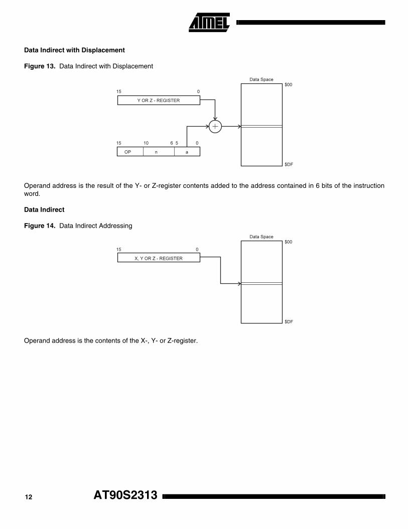
Data Indirect with Displacement
Figure 13. Data Indirect with Displacement
Operand address is the result of the Y- or Z-register contents added to the address contained in 6 bits of the instructionword.
Data Indirect
Figure 14. Data Indirect Addressing
Operand address is the contents of the X-, Y- or Z-register.
AT90S231312

AT90S2313
Data Indirect with Pre-decrement
Figure 15. Data Indirect Addressing with Pre-decrement
The X-, Y- or Z-register is decremented before the operation. Operand address is the decremented contents of the X-, Y- orZ-register.
Data Indirect with Post-increment
Figure 16. Data Indirect Addressing with Post-increment
The X-, Y- or Z-register is incremented after the operation. Operand address is the contents of the X-, Y- or Z-register priorto incrementing.
13

Constant Addressing Using the LPM Instruction
Figure 17. Code Memory Constant Addressing
Constant byte address is specified by the Z-register contents. The 15 MSBs select word address (0 - 1K), the LSB selectslow byte if cleared (LSB = 0) or high byte if set (LSB = 1).
Indirect Program Addressing, IJMP and ICALL
Figure 18. Indirect Program Memory Addressing
Program execution continues at address contained by the Z-register (i.e., the PC is loaded with the contents of theZ-register).
AT90S231314

AT90S2313
Relative Program Addressing, RJMP and RCALL
Figure 19. Relative Program Memory Addressing
Program execution continues at address PC + k + 1. The relative address k is -2048 to 2047.
Memory Access and Instruction Execution TimingThis section describes the general access timing concepts for instruction execution and internal memory access.
The AVR CPU is driven by the System Clock Ø, directly generated from the external clock crystal for the chip. No internalclock division is used.
Figure 20 shows the parallel instruction fetches and instruction executions enabled by the Harvard architecture and thefast-access register file concept. This is the basic pipelining concept to obtain up to 1 MIPS per MHz with the correspondingunique results for functions per cost, functions per clocks and functions per power-unit.
Figure 20. The Parallel Instruction Fetches and Instruction Executions
Figure 21 shows the internal timing concept for the register file. In a single clock cycle an ALU operation using two registeroperands is executed, and the result is stored back to the destination register.
System Clock Ø
1st Instruction Fetch
1st Instruction Execute2nd Instruction Fetch
2nd Instruction Execute3rd Instruction Fetch
3rd Instruction Execute4th Instruction Fetch
T1 T2 T3 T4
15

Figure 21. Single-cycle ALU Operation
The internal data SRAM access is performed in two System Clock cycles as described in Figure 22.
Figure 22. On-chip Data SRAM Access Cycles
System Clock Ø
Total Execution Time
Register Operands Fetch
ALU Operation Execute
Result Write Back
T1 T2 T3 T4
System Clock Ø
WR
RD
Data
Data
Address Address
T1 T2 T3 T4
Prev. Address
Rea
dW
rite
AT90S231316
AT90S2313
I/O MemoryThe I/O space definition of the AT90S2313 is shown in Table 1.
Note: Reserved and unused locations are not shown in the table.
Table 1. AT90S2313 I/O Space
Address Hex Name Function
$3F ($5F) SREG Status Register
$3D ($5D) SPL Stack Pointer Low
$3B ($5B) GIMSK General Interrupt MaSK register
$3A ($5A) GIFR General Interrupt Flag Register
$39 ($59) TIMSK Timer/Counter Interrupt MaSK register
$38 ($58) TIFR Timer/Counter Interrupt Flag register
$35 ($55) MCUCR MCU general Control Register
$33 ($53) TCCR0 Timer/Counter 0 Control Register
$32 ($52) TCNT0 Timer/Counter 0 (8-bit)
$2F ($4F) TCCR1A Timer/Counter 1 Control Register A
$2E ($4E) TCCR1B Timer/Counter 1 Control Register B
$2D ($4D) TCNT1H Timer/Counter 1 High Byte
$2C ($4C) TCNT1L Timer/Counter 1 Low Byte
$2B ($4B) OCR1AH Output Compare Register 1 High Byte
$2A ($4A) OCR1AL Output Compare Register 1 Low Byte
$25 ($45) ICR1H T/C 1 Input Capture Register High Byte
$24 ($44) ICR1L T/C 1 Input Capture Register Low Byte
$21 ($41) WDTCR Watchdog Timer Control Register
$1E ($3E) EEAR EEPROM Address Register
$1D ($3D) EEDR EEPROM Data Register
$1C ($3C) EECR EEPROM Control Register
$18 ($38) PORTB Data Register, Port B
$17 ($37) DDRB Data Direction Register, Port B
$16 ($36) PINB Input Pins, Port B
$12 ($32) PORTD Data Register, Port D
$11 ($31) DDRD Data Direction Register, Port D
$10 ($30) PIND Input Pins, Port D
$0C ($2C) UDR UART I/O Data Register
$0B ($2B) USR UART Status Register
$0A ($2A) UCR UART Control Register
$09 ($29) UBRR UART Baud Rate Register
$08 ($28) ACSR Analog Comparator Control and Status Register
17

All AT90S2313 I/O and peripherals are placed in the I/O space. The I/O locations are accessed by the IN and OUT instruc-tions transferring data between the 32 general-purpose working registers and the I/O space. I/O registers within theaddress range $00 - $1F are directly bit-accessible using the SBI and CBI instructions. In these registers, the value of sin-gle bits can be checked by using the SBIS and SBIC instructions. Refer to the instruction set section for more details. Whenusing the I/O specific commands IN and OUT, the I/O addresses $00 - $3F must be used. When addressing I/O registersas SRAM, $20 must be added to this address. All I/O register addresses throughout this document are shown with theSRAM address in parentheses.
For compatibility with future devices, reserved bits should be written to zero if accessed. Reserved I/O memory addressesshould never be written.
Some of the status flags are cleared by writing a logical “1” to them. Note that the CBI and SBI instructions will operate onall bits in the I/O register, writing a “1” back into any flag read as set, thus clearing the flag. The CBI and SBI instructionswork with registers $00 to $1F only.
The I/O and peripherals control registers are explained in the following sections.
Status Register – SREG
The AVR Status Register (SREG) at I/O space location $3F ($5F) is defined as:
• Bit 7 – I: Global Interrupt Enable
The global interrupt enable bit must be set (one) for the interrupts to be enabled. The individual interrupt enable control isthen performed in separate control registers. If the global interrupt enable bit is cleared (zero), none of the interrupts areenabled independent of the individual interrupt enable settings. The I-bit is cleared by hardware after an interrupt hasoccurred, and is set by the RETI instruction to enable subsequent interrupts.• Bit 6 – T: Bit Copy Storage
The bit copy instructions BLD (Bit LoaD) and BST (Bit STore) use the T-bit as source and destination for the operated bit.A bit from a register in the register file can be copied into T by the BST instruction, and a bit in T can be copied into a bit ina register in the register file by the BLD instruction.• Bit 5 – H: Half-carry Flag
The half-carry flag H indicates a half-carry in some arithmetic operations. See the Instruction Set description for detailedinformation.• Bit 4 – S: Sign Bit, S = N ⊕ V
The S-bit is always an exclusive or between the negative flag N and the two’s complement overflow flag V. See the Instruc-tion Set description for detailed information.• Bit 3 – V: Two’s Complement Overflow Flag
The two’s complement overflow flag V supports two’s complement arithmetics. See the Instruction Set description fordetailed information.• Bit 2 – N: Negative Flag
The negative flag N indicates a negative result after the different arithmetic and logic operations. See the Instruction Setdescription for detailed information.• Bit 1 – Z: Zero Flag
The zero flag Z indicates a zero result after the different arithmetic and logic operations. See the Instruction Set descriptionfor detailed information.• Bit 0 – C: Carry Flag
The carry flag C indicates a carry in an arithmetic or logic operation. See the Instruction Set description for detailedinformation.
Note that the Status Register is not automatically stored when entering an interrupt routine and restored when returningfrom an interrupt routine. This must be handled by software.
Bit 7 6 5 4 3 2 1 0
$3F ($5F) I T H S V N Z C SREG
Read/Write R/W R/W R/W R/W R/W R/W R/W R/W
Initial value 0 0 0 0 0 0 0 0
AT90S231318

AT90S2313
Stack Pointer – SP
An 8-bit register at I/O address $3D ($5D) forms the stack pointer of the AT90S2313. 8 bits are used to address the128 bytes of SRAM in locations $60 - $DF.
The Stack Pointer points to the data SRAM stack area where the Subroutine and Interrupt stacks are located. This stackspace in the data SRAM must be defined by the program before any subroutine calls are executed or interrupts areenabled. The Stack Pointer must be set to point above $60. The Stack Pointer is decremented by 1 when data is pushedonto the stack with the PUSH instruction, and it is decremented by 2 when an address is pushed onto the stack with sub-routine calls and interrupts. The Stack Pointer is incremented by 1 when data is popped from the stack with the POPinstruction, and it is incremented by 2 when an address is popped from the stack with return from subroutine RET or returnfrom interrupt RETI.
Reset and Interrupt HandlingThe AT90S2313 provides 10 different interrupt sources. These interrupts and the separate reset vector each have a sepa-rate program vector in the program memory space. All the interrupts are assigned individual enable bits that must be set(one) together with the I-bit in the Status Register in order to enable the interrupt.
The lowest addresses in the program memory space are automatically defined as the Reset and Interrupt vectors. Thecomplete list of vectors is shown in Table 2. The list also determines the priority levels of the different interrupts. The lowerthe address, the higher the priority level. RESET has the highest priority, and next is INT0 (the External Interrupt Request0), etc.
Bit 7 6 5 4 3 2 1 0
$3D ($5D) SP7 SP6 SP5 SP4 SP3 SP2 SP1 SP0 SPL
Read/Write R/W R/W R/W R/W R/W R/W R/W R/W
Initial value 0 0 0 0 0 0 0 0
Table 2. Reset and Interrupt Vectors
Vector No. Program Address Source Interrupt Definition
1 $000 RESET Hardware Pin, Power-on Reset and Watchdog Reset
2 $001 INT0 External Interrupt Request 0
3 $002 INT1 External Interrupt Request 1
4 $003 TIMER1 CAPT1 Timer/Counter1 Capture Event
5 $004 TIMER1 COMP1 Timer/Counter1 Compare Match
6 $005 TIMER1 OVF1 Timer/Counter1 Overflow
7 $006 TIMER0 OVF0 Timer/Counter0 Overflow
8 $007 UART, RX UART, RX Complete
9 $008 UART, UDRE UART Data Register Empty
10 $009 UART, TX UART, TX Complete
11 $00A ANA_COMP Analog Comparator
19

The most typical and general program setup for the Reset and Interrupt vector addresses are:Address Labels Code Comments
$000 rjmp RESET ; Reset Handler
$001 rjmp EXT_INT0 ; IRQ0 Handler
$002 rjmp EXT_INT1 ; IRQ1 Handler
$003 rjmp TIM_CAPT1 ; Timer1 Capture Handler
$004 rjmp TIM_COMP1 ; Timer1 Compare Handler
$005 rjmp TIM_OVF1 ; Timer1 Overflow Handler
$006 rjmp TIM_OVF0 ; Timer0 Overflow Handler
$007 rjmp UART_RXC ; UART RX Complete Handler
$008 rjmp UART_DRE ; UDR Empty Handler
$009 rjmp UART_TXC ; UART TX Complete Handler
$00a rjmp ANA_COMP ; Analog Comparator Handler
;
$00b MAIN: ldi r16,low(RAMEND); Main program start
$00c out SPL,r16$00d <instr> xxx… … … …
Reset Sources
The AT90S2313 has three sources of reset:• Power-on Reset. The MCU is reset when the supply voltage is below the Power-on Reset threshold (VPOT).
• External Reset. The MCU is reset when a low level is present on the RESET pin for more than 50 ns.
• Watchdog Reset. The MCU is reset when the Watchdog timer period expires and the Watchdog is enabled.
During reset, all I/O registers are then set to their initial values, and the program starts execution from address $000. Theinstruction placed in address $000 must be an RJMP (relative jump) instruction to the reset handling routine. If theprogram never enables an interrupt source, the interrupt vectors are not used, and regular program code can be placed atthese locations. The circuit diagram in Figure 23 shows the reset logic. Table 3 defines the timing and electrical parametersof the reset circuitry.
Figure 23. Reset Logic
AT90S231320

AT90S2313
Note: 1. The Power-on Reset will not work unless the supply voltage has been below VPOT (falling).
The user can select the start-up time according to typical oscillator start-up. The number of WDT oscillator cycles used foreach time-out is shown in Table 4. The frequency of the Watchdog Oscillator is voltage-dependent, as shown in “TypicalCharacteristics” on page 72.
Power-on Reset
A Power-on Reset (POR) circuit ensures that the device is reset from power-on. As shown in Figure 23, an internal timer isclocked from the Watchdog Timer. This timer prevents the MCU from starting until after a certain period after VCC hasreached the Power-on Threshold voltage (VPOT) (see Figure 24). The FSTRT Fuse bit in the Flash can be programmed togive a shorter start-up time if a ceramic resonator or any other fast-start oscillator is used to clock the MCU.
If the built-in start-up delay is sufficient, RESET can be connected to VCC directly or via an external pull-up resistor. Byholding the RESET pin low for a period after VCC has been applied, the Power-on Reset period can be extended. Refer toFigure 25 for a timing example of this.
Figure 24. MCU Start-up, RESET Tied to VCC.
Table 3. Reset Characteristics (VCC = 5.0V)
Symbol Parameter Min Typ Max Units
VPOT(1)
Power-on Reset Threshold Voltage (rising) 1.0 1.4 1.8 V
Power-on Reset Threshold Voltage (falling) 0.4 0.6 0.8 V
VRST RESET Pin Threshold Voltage – 0.85 VCC V
tTOUT Reset Delay Time-out PeriodFSTRT Unprogrammed
11.0 16.0 21.0 ms
tTOUT Reset Delay Time-out PeriodFSTRT Programmed
1.0 1.1 1.2 ms
Table 4. Number of Watchdog Oscillator Cycles
FSTRT Time-out at VCC = 5V Number of WDT Cycles
Programmed 1.1 ms 1K
Unprogrammed 16.0 ms 16K
VCC
RESET
TIME-OUT
INTERNALRESET
tTOUT
VPOT
VRST
21
Figure 25. MCU Start-up, RESET Controlled Externally
External Reset
An external reset is generated by a low level on the RESET pin. Reset pulses longer than 50 ns will generate a reset, evenif the clock is not running. Shorter pulses are not guaranteed to generate a reset. When the applied signal reaches theReset Threshold Voltage (VRST) on its positive edge, the delay timer starts the MCU after the Time-out period tTOUT hasexpired.
Figure 26. External Reset during Operation
VCC
RESET
TIME-OUT
INTERNALRESET
tTOUT
VPOT
VRST
AT90S231322

AT90S2313
Watchdog Reset
When the Watchdog times out, it will generate a short reset pulse of one XTAL cycle duration. On the falling edge of thispulse, the delay timer starts counting the Time-out period tTOUT. Refer to page 36 for details on operation of the Watchdog.
Figure 27. Watchdog Reset during Operation
Interrupt Handling
The AT90S2313 has two 8-bit Interrupt Mask control registers: the GIMSK (General Interrupt Mask register) and the TIMSK(Timer/Counter Interrupt Mask register).
When an interrupt occurs, the Global Interrupt Enable I-bit is cleared (zero) and all interrupts are disabled. The user soft-ware can set (one) the I-bit to enable interrupts. The I-bit is set (one) when a Return from Interrupt instruction (RETI) isexecuted.
For interrupts triggered by events that can remain static (e.g., the Output Compare Register1 matching the value ofTimer/Counter1), the interrupt flag is set when the event occurs. If the interrupt flag is cleared and the interrupt conditionpersists, the flag will not be set until the event occurs the next time.
When the Program Counter is vectored to the actual interrupt vector in order to execute the interrupt handling routine, hard-ware clears the corresponding flag that generated the interrupt. Some of the interrupt flags can also be cleared by writing alogical “1” to the flag bit position(s) to be cleared.
If an interrupt condition occurs when the corresponding interrupt enable bit is cleared (zero), the interrupt flag will be setand remembered until the interrupt is enabled, or the flag is cleared by software.
If one or more interrupt conditions occur when the global interrupt enable bit is cleared (zero), the corresponding interruptflag(s) will be set and remembered until the global interrupt enable bit is set (one), and will be executed by order of priority.
Note that external level interrupt does not have a flag, and will only be remembered for as long as the interrupt condition isactive.
Note that the Status Register is not automatically stored when entering an interrupt routine and restored when returningfrom an interrupt routine. This must be handled by software.
23
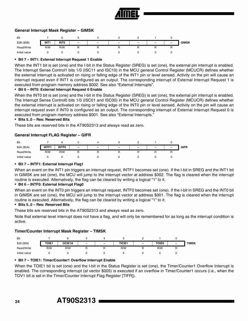
General Interrupt Mask Register – GIMSK
• Bit 7 – INT1: External Interrupt Request 1 Enable
When the INT1 bit is set (one) and the I-bit in the Status Register (SREG) is set (one), the external pin interrupt is enabled.The Interrupt Sense Control1 bits 1/0 (ISC11 and ISC10) in the MCU general Control Register (MCUCR) defines whetherthe external interrupt is activated on rising or falling edge of the INT1 pin or level sensed. Activity on the pin will cause aninterrupt request even if INT1 is configured as an output. The corresponding interrupt of External Interrupt Request 1 isexecuted from program memory address $002. See also “External Interrupts”.• Bit 6 – INT0: External Interrupt Request 0 Enable
When the INT0 bit is set (one) and the I-bit in the Status Register (SREG) is set (one), the external pin interrupt is enabled.The Interrupt Sense Control0 bits 1/0 (ISC01 and ISC00) in the MCU general Control Register (MCUCR) defines whetherthe external interrupt is activated on rising or falling edge of the INT0 pin or level sensed. Activity on the pin will cause aninterrupt request even if INT0 is configured as an output. The corresponding interrupt of External Interrupt Request 0 isexecuted from program memory address $001. See also “External Interrupts.”• Bits 5..0 – Res: Reserved Bits
These bits are reserved bits in the AT90S2313 and always read as zero.
General Interrupt FLAG Register – GIFR
• Bit 7 – INTF1: External Interrupt Flag1
When an event on the INT1 pin triggers an interrupt request, INTF1 becomes set (one). If the I-bit in SREG and the INT1 bitin GIMSK are set (one), the MCU will jump to the interrupt vector at address $002. The flag is cleared when the interruptroutine is executed. Alternatively, the flag can be cleared by writing a logical “1” to it.• Bit 6 – INTF0: External Interrupt Flag0
When an event on the INT0 pin triggers an interrupt request, INTF0 becomes set (one). If the I-bit in SREG and the INT0 bitin GIMSK are set (one), the MCU will jump to the interrupt vector at address $001. The flag is cleared when the interruptroutine is executed. Alternatively, the flag can be cleared by writing a logical “1” to it.• Bits 5..0 – Res: Reserved Bits
These bits are reserved bits in the AT90S2313 and always read as zero.
Note that external level interrupt does not have a flag, and will only be remembered for as long as the interrupt condition isactive.
Timer/Counter Interrupt Mask Register – TIMSK
• Bit 7 – TOIE1: Timer/Counter1 Overflow Interrupt Enable
When the TOIE1 bit is set (one) and the I-bit in the Status Register is set (one), the Timer/Counter1 Overflow Interrupt isenabled. The corresponding interrupt (at vector $005) is executed if an overflow in Timer/Counter1 occurs (i.e., when theTOV1 bit is set in the Timer/Counter Interrupt Flag Register [TIFR]).
Bit 7 6 5 4 3 2 1 0
$3B ($5B) INT1 INT0 – – – – – – GIMSK
Read/Write R/W R/W R R R R R R
Initial value 0 0 0 0 0 0 0 0
Bit 7 6 5 4 3 2 1 0
$3A ($5A) INTF1 INTF0 – – – – – – GIFR
Read/Write R/W R/W R R R R R R
Initial value 0 0 0 0 0 0 0 0
Bit 7 6 5 4 3 2 1 0
$39 ($59) TOIE1 OCIE1A – – TICIE1 – TOIE0 – TIMSK
Read/Write R/W R/W R R R/W R R/W R
Initial value 0 0 0 0 0 0 0 0
AT90S231324

AT90S2313
• Bit 6 – OCIE1A: Timer/Counter1 Output Compare Match Interrupt Enable
When the OCIE1A bit is set (one) and the I-bit in the Status Register is set (one), the Timer/Counter1 Compare Match Inter-rupt is enabled. The corresponding interrupt (at vector $004) is executed if a compare match in Timer/Counter1 occurs (i.e.,when the OCF1A bit is set in the Timer/Counter Interrupt Flag Register [TIFR]).• Bit 5,4 – Res: Reserved Bits
These bits are reserved bits in the AT90S2313 and always read as zero.• Bit 3 – TICIE1: Timer/Counter1 Input Capture Interrupt Enable
When the TICIE1 bit is set (one) and the I-bit in the Status Register is set (one), the Timer/Counter1 Input Capture EventInterrupt is enabled. The corresponding interrupt (at vector $003) is executed if a capture-triggering event occurs onPD6(ICP) (i.e., when the ICF1 bit is set in the Timer/Counter Interrupt Flag Register [TIFR]).• Bit 2 – Res: Reserved Bit
This bit is a reserved bit in the AT90S2313 and always reads as zero.• Bit 1 – TOIE0: Timer/Counter0 Overflow Interrupt Enable
When the TOIE0 bit is set (one) and the I-bit in the Status Register is set (one), the Timer/Counter0 Overflow Interrupt isenabled. The corresponding interrupt (at vector $006) is executed if an overflow in Timer/Counter0 occurs (i.e., when theTOV0 bit is set in the Timer/Counter Interrupt Flag Register [TIFR]).• Bit 0 – Res: Reserved Bit
This bit is a reserved bit in the AT90S2313 and always read as zero.
Timer/Counter Interrupt FLAG Register – TIFR
• Bit 7 – TOV1: Timer/Counter1 Overflow Flag
The TOV1 is set (one) when an overflow occurs in Timer/Counter1. TOV1 is cleared by hardware when executing thecorresponding interrupt handling vector. Alternatively, TOV1 is cleared by writing a logical “1” to the flag. When the I-bit inSREG and TOIE1 (Timer/Counter1 Overflow Interrupt Enable) and TOV1 are set (one), the Timer/Counter1 Overflow Inter-rupt is executed. In PWM mode, this bit is set when Timer/Counter1 changes counting direction at $0000.• Bit 6 – OCF1A: Output Compare Flag 1A
The OCF1A bit is set (one) when a compare match occurs between the Timer/Counter1 and the data in OCR1A (OutputCompare Register1 A). OCF1A is cleared by hardware when executing the corresponding interrupt handling vector. Alter-natively, OCF1A is cleared by writing a logical “1” to the flag. When the I-bit in SREG and OCIE1A (Timer/Counter1Compare Match Interrupt Enable) and the OCF1A are set (one), the Timer/Counter1 Compare Match Interrupt is executed.• Bits 5, 4 – Res: Reserved Bits
These bits are reserved bits in the AT90S2313 and always read as zero.• Bit 3 – ICF1: Input Capture Flag 1
The ICF1 bit is set (one) to flag an input capture event, indicating that the Timer/Counter1 value has been transferred to theInput Capture Register (ICR1). ICF1 is cleared by hardware when executing the corresponding interrupt handling vector.Alternatively, ICF1 is cleared by writing a logical “1” to the flag. When the SREG I-bit and TICIE1 (Timer/Counter1 InputCapture Interrupt Enable) and ICF1 are set (one), the Timer/Counter1 Capture Interrupt is executed.• Bit 2 – Res: Reserved Bit
This bit is a reserved bit in the AT90S2313 and always reads as zero.• Bit 1 – TOV0: Timer/Counter0 Overflow Flag
The bit TOV0 is set (one) when an overflow occurs in Timer/Counter0. TOV0 is cleared by hardware when executing thecorresponding interrupt handling vector. Alternatively, TOV0 is cleared by writing a logical “1” to the flag. When the SREGI-bit and TOIE0 (Timer/Counter0 Overflow Interrupt Enable) and TOV0 are set (one), the Timer/Counter0 Overflow Inter-rupt is executed.• Bit 0 – Res: Reserved Bit
This bit is a reserved bit in the AT90S2313 and always reads as zero.
Bit 7 6 5 4 3 2 1 0
$38 ($58) TOV1 OCF1A – – ICF1 – TOV0 – TIFR
Read/Write R/W R/W R R R/W R R/W R
Initial value 0 0 0 0 0 0 0 0
25
External Interrupts
The External Interrupts are triggered by the INT1 and INT0 pins. Observe that, if enabled, the interrupts will trigger even ifthe INT0/INT1 pins are configured as outputs. This feature provides a way of generating a software interrupt. The ExternalInterrupts can be triggered by a falling or rising edge or a low level. This is set up as indicated in the specification for theMCU Control Register (MCUCR). When the External Interrupt is enabled and is configured as level-triggered, the interruptwill trigger as long as the pin is held low.
The External Interrupts are set up as described in the specification for the MCU Control Register (MCUCR).
Interrupt Response Time
The interrupt execution response for all the enabled AVR interrupts is four clock cycles, minimum. Four clock cycles afterthe interrupt flag has been set, the program vector address for the actual interrupt handling routine is executed. During this4-clock-cycle period, the Program Counter (2 bytes) is pushed onto the stack, and the Stack Pointer is decremented by 2.The vector is normally a relative jump to the interrupt routine, and this jump takes two clock cycles. If an interrupt occursduring execution of a multi-cycle instruction, this instruction is completed before the interrupt is served.A return from an interrupt handling routine takes four clock cycles. During these four clock cycles, the Program Counter (2bytes) is popped back from the stack, the Stack Pointer is incremented by 2, and the I-flag in SREG is set. When the AVRexits from an interrupt, it will always return to the main program and execute one more instruction before any pending inter-rupt is served.
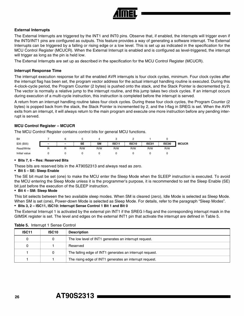
MCU Control Register – MCUCR
The MCU Control Register contains control bits for general MCU functions.
• Bits 7, 6 – Res: Reserved Bits
These bits are reserved bits in the AT90S2313 and always read as zero.• Bit 5 – SE: Sleep Enable
The SE bit must be set (one) to make the MCU enter the Sleep Mode when the SLEEP instruction is executed. To avoidthe MCU entering the Sleep Mode unless it is the programmer’s purpose, it is recommended to set the Sleep Enable (SE)bit just before the execution of the SLEEP instruction.• Bit 4 – SM: Sleep Mode
This bit selects between the two available sleep modes. When SM is cleared (zero), Idle Mode is selected as Sleep Mode.When SM is set (one), Power-down Mode is selected as Sleep Mode. For details, refer to the paragraph “Sleep Modes”.• Bits 3, 2 – ISC11, ISC10: Interrupt Sense Control 1 Bit 1 and Bit 0
The External Interrupt 1 is activated by the external pin INT1 if the SREG I-flag and the corresponding interrupt mask in theGIMSK register is set. The level and edges on the external INT1 pin that activate the interrupt are defined in Table 5.
Bit 7 6 5 4 3 2 1 0
$35 ($55) – – SE SM ISC11 ISC10 ISC01 ISC00 MCUCR
Read/Write R R R/W R/W R/W R/W R/W R/W
Initial value 0 0 0 0 0 0 0 0
Table 5. Interrupt 1 Sense Control
ISC11 ISC10 Description
0 0 The low level of INT1 generates an interrupt request.
0 1 Reserved
1 0 The falling edge of INT1 generates an interrupt request.
1 1 The rising edge of INT1 generates an interrupt request.
AT90S231326
AT90S2313
• Bits 1, 0 – ISC01, ISC00: Interrupt Sense Control 0 Bit 1 and Bit 0
The External Interrupt 0 is activated by the external pin INT0 if the SREG I-flag and the corresponding interrupt mask is set.The level and edges on the external INT0 pin that activate the interrupt are defined in Table 6.
The value on the INTn pin is sampled before detecting edges. If edge interrupt is selected, pulses with a duration longerthan one CPU clock period will generate an interrupt. Shorter pulses are not guaranteed to generate an interrupt. If low-level interrupt is selected, the low level must be held until the completion of the currently executing instruction to generatean interrupt. If enabled, a level-triggered interrupt will generate an interrupt request as long as the pin is held low.
Sleep ModesTo enter the sleep modes, the SE bit in MCUCR must be set (one) and a SLEEP instruction must be executed. If anenabled interrupt occurs while the MCU is in a sleep mode, the MCU awakes, executes the interrupt routine, and resumesexecution from the instruction following SLEEP. The contents of the register file, SRAM and I/O memory are unaltered. If areset occurs during Sleep Mode, the MCU wakes up and executes from the Reset vector.
Idle Mode
When the SM bit is cleared (zero), the SLEEP instruction forces the MCU into the Idle Mode, stopping the CPU but allowingTimer/Counters, Watchdog and the interrupt system to continue operating. This enables the MCU to wake up from externaltriggered interrupts as well as internal ones like Timer Overflow interrupt and Watchdog reset. If wake-up from the AnalogComparator Interrupt is not required, the Analog Comparator can be powered down by setting the ACD-bit in the AnalogComparator Control and Status Register (ACSR). This will reduce power consumption in Idle Mode. When the MCU wakesup from Idle Mode, the CPU starts program execution immediately.
Power-down Mode
When the SM bit is set (one), the SLEEP instruction forces the MCU into the Power-down Mode. In this mode, the externaloscillator is stopped while the external interrupts and the Watchdog (if enabled) continue operating. Only an external reset,a Watchdog reset (if enabled), an external level interrupt on INT0 or INT1 can wake up the MCU.
Note that when a level-triggered interrupt is used for wake-up from power-down, the low level must be held for a timelonger than the reset delay Time-out period tTOUT. Otherwise, the device will not wake up.
Timer/CountersThe AT90S2313 provides two general-purpose Timer/Counters – one 8-bit T/C and one 16-bit T/C. The Timer/Countershave individual prescaling selection from the same 10-bit prescaling timer. Both Timer/Counters can either be used as atimer with an internal clock time base or as a counter with an external pin connection that triggers the counting.
Table 6. Interrupt 0 Sense Control
ISC01 ISC00 Description
0 0 The low level of INT0 generates an interrupt request.
0 1 Reserved
1 0 The falling edge of INT0 generates an interrupt request.
1 1 The rising edge of INT0 generates an interrupt request.
27
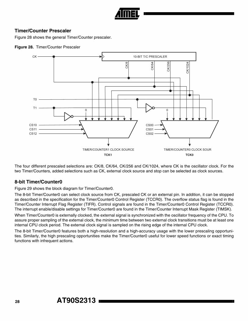
Timer/Counter PrescalerFigure 28 shows the general Timer/Counter prescaler.
Figure 28. Timer/Counter Prescaler
The four different prescaled selections are: CK/8, CK/64, CK/256 and CK/1024, where CK is the oscillator clock. For thetwo Timer/Counters, added selections such as CK, external clock source and stop can be selected as clock sources.
8-bit Timer/Counter0Figure 29 shows the block diagram for Timer/Counter0.
The 8-bit Timer/Counter0 can select clock source from CK, prescaled CK or an external pin. In addition, it can be stoppedas described in the specification for the Timer/Counter0 Control Register (TCCR0). The overflow status flag is found in theTimer/Counter Interrupt Flag Register (TIFR). Control signals are found in the Timer/Counter0 Control Register (TCCR0).The interrupt enable/disable settings for Timer/Counter0 are found in the Timer/Counter Interrupt Mask Register (TIMSK).
When Timer/Counter0 is externally clocked, the external signal is synchronized with the oscillator frequency of the CPU. Toassure proper sampling of the external clock, the minimum time between two external clock transitions must be at least oneinternal CPU clock period. The external clock signal is sampled on the rising edge of the internal CPU clock.
The 8-bit Timer/Counter0 features both a high-resolution and a high-accuracy usage with the lower prescaling opportuni-ties. Similarly, the high prescaling opportunities make the Timer/Counter0 useful for lower speed functions or exact timingfunctions with infrequent actions.
TCK1 TCK0
AT90S231328

AT90S2313
Figure 29. Timer/Counter0 Block Diagram
Timer/Counter0 Control Register – TCCR0
• Bits 7..3 – Res: Reserved Bits
These bits are reserved bits in the AT90S2313 and always read zero.• Bits 2,1,0 – CS02, CS01, CS00: Clock Select0, Bit 2,1 and 0
The Clock Select0 bits 2, 1 and 0 define the prescaling source of Timer/Counter0.
Bit 7 6 5 4 3 2 1 0
$33 ($53) – – – – – CS02 CS01 CS00 TCCR0
Read/Write R R R R R R/W R/W R/W
Initial value 0 0 0 0 0 0 0 0
Table 7. Clock 0 Prescale Select
CS02 CS01 CS00 Description
0 0 0 Stop, the Timer/Counter0 is stopped.
0 0 1 CK
0 1 0 CK/8
0 1 1 CK/64
1 0 0 CK/256
1 0 1 CK/1024
1 1 0 External Pin T0, falling edge
1 1 1 External Pin T0, rising edge
T0
29
The Stop condition provides a Timer Enable/Disable function. The CK down divided modes are scaled directly from the CKoscillator clock. If the external pin modes are used for Timer/Counter0, transitions on PD4/(T0) will clock the counter even ifthe pin is configured as an output. This feature can give the user software control of the counting.
Timer/Counter0 – TCNT0
The Timer/Counter0 is realized as an up-counter with read and write access. If the Timer/Counter0 is written and a clocksource is present, the Timer/Counter0 continues counting in the timer clock cycle following the write operation.
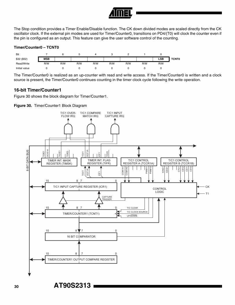
16-bit Timer/Counter1Figure 30 shows the block diagram for Timer/Counter1.
Figure 30. Timer/Counter1 Block Diagram
Bit 7 6 5 4 3 2 1 0
$32 ($52) MSB LSB TCNT0
Read/Write R/W R/W R/W R/W R/W R/W R/W R/W
Initial value 0 0 0 0 0 0 0 0
T1
AT90S231330

AT90S2313
The 16-bit Timer/Counter1 can select clock source from CK, prescaled CK or an external pin. In addition, it can be stoppedas described in the specification for the Timer/Counter1 Control Register (TCCR1B). The different status flags (Overflow,Compare Match and Capture Event) and control signals are found in the Timer/Counter Interrupt Flag Register (TIFR). Theinterrupt enable/disable settings for Timer/Counter1 are found in the Timer/Counter Interrupt Mask Register (TIMSK).
When Timer/Counter1 is externally clocked, the external signal is synchronized with the oscillator frequency of the CPU. Toassure proper sampling of the external clock, the minimum time between two external clock transitions must be at least oneinternal CPU clock period. The external clock signal is sampled on the rising edge of the internal CPU clock.
The 16-bit Timer/Counter1 features both a high-resolution and a high-accuracy usage with the lower prescaling opportuni-ties. Similarly, the high prescaling opportunities makes the Timer/Counter1 useful for lower speed functions or exact timingfunctions with infrequent actions.
The Timer/Counter1 supports an Output Compare function using the Output Compare Register 1A (OCR1A) as the datasource to be compared to the Timer/Counter1 contents. The Output Compare functions include optional clearing of thecounter on compare matches, and actions on the Output Compare pin 1 on compare matches.
Timer/Counter1 can also be used as an 8-, 9- or 10-bit Pulse Width Modulator. In this mode the counter and the OCR1 reg-ister serve as a glitch-free standalone PWM with centered pulses. Refer to page 35 for a detailed description of thisfunction.
The Input Capture function of Timer/Counter1 provides a capture of the Timer/Counter1 contents to the Input Capture Reg-ister (ICR1), triggered by an external event on the Input Capture Pin (ICP). The actual capture event settings are defined bythe Timer/Counter1 Control Register (TCCR1B). In addition, the Analog Comparator can be set to trigger the input capture.Refer to “Analog Comparator” on page 46 for details on this. The ICP pin logic is shown in Figure 31.
Figure 31. ICP Pin Schematic Diagram
If the Noise Canceler function is enabled, the actual trigger condition for the capture event is monitored over four samples,and all four must be equal to activate the capture flag.
31
Timer/Counter1 Control Register A – TCCR1A
• Bits 7,6 – COM1A1, COM1A0: Compare Output Mode1, Bits 1 and 0
The COM1A1 and COM1A0 control bits determine any output pin action following a compare match in Timer/Counter1.Any output pin actions affect pin OC1 (Output Compare pin 1) (PB3). This is an alternative function to the I/O port, and thecorresponding direction control bit must be set (one) to control an output pin. The control configuration is shown in Table 8.
Note: In PWM mode, these bits have a different function. Refer to Table 12 for a detailed description.
• Bits 5..2 – Res: Reserved Bits
These bits are reserved bits in the AT90S2313 and always read zero.• Bits 1,0 – PWM11, PWM10: Pulse Width Modulator Select Bits
These bits select PWM operation of Timer/Counter1 as specified in Table 9. This mode is described on page 35.
Timer/Counter1 Control Register B – TCCR1B
• Bit 7 – ICNC1: Input Capture1 Noise Canceler (4 CKs)
When the ICNC1 bit is cleared (zero), the input capture trigger noise canceler function is disabled. The input capture is trig-gered at the first rising/falling edge sampled on the ICP (input capture pin) as specified. When the ICNC1 bit is set (one),four successive samples are measured on the ICP (input capture pin), and all samples must be high/low according to theinput capture trigger specification in the ICES1 bit. The actual sampling frequency is the XTAL clock frequency.• Bit 6 – ICES1: Input Capture1 Edge Select
While the ICES1 bit is cleared (zero), the Timer/Counter1 contents are transferred to the Input Capture Register (ICR1) onthe falling edge of the input capture pin (ICP). While the ICES1 bit is set (one), the Timer/Counter1 contents are transferredto the Input Capture Register (ICR1) on the rising edge of the input capture pin (ICP).• Bits 5, 4 – Res: Reserved Bits
These bits are reserved bits in the AT90S2313 and always read zero.
Bit 7 6 5 4 3 2 1 0
$2F ($4F) COM1A1 COM1A0 – – – – PWM11 PWM10 TCCR1A
Read/Write R/W R/W R R R R R/W R/W
Initial value 0 0 0 0 0 0 0 0
Table 8. Compare 1 Mode Select
COM1A1 COM1A0 Description
0 0 Timer/Counter1 disconnected from output pin OC1
0 1 Toggle the OC1 output line.
1 0 Clear the OC1 output line (to zero).
1 1 Set the OC1 output line (to one).
Table 9. PWM Mode Select
PWM11 PWM10 Description
0 0 PWM operation of Timer/Counter1 is disabled
0 1 Timer/Counter1 is an 8-bit PWM
1 0 Timer/Counter1 is a 9-bit PWM
1 1 Timer/Counter1 is a 10-bit PWM
Bit 7 6 5 4 3 2 1 0
$2E ($4E) ICNC1 ICES1 – – CTC1 CS12 CS11 CS10 TCCR1B
Read/Write R/W R/W R R R/W R/W R/W R/W
Initial value 0 0 0 0 0 0 0 0
AT90S231332
AT90S2313
• Bit 3 – CTC1: Clear Timer/Counter1 on Compare Match
When the CTC1 control bit is set (one), the Timer/Counter1 is reset to $0000 in the clock cycle after a compareA match. Ifthe CTC1 control bit is cleared, Timer/Counter1 continues counting and is unaffected by a compare match. Since the com-pare match is detected in the CPU clock cycle following the match, this function will behave differently when a prescalinghigher than 1 is used for the timer. When a prescaling of 1 is used, and the compareA register is set to C, the timer willcount as follows if CTC1 is set:
... | C-2 | C-1 | C | 0 | 1 |...
When the prescaler is set to divide by 8, the timer will count like this:
... | C-2, C-2, C-2, C-2, C-2, C-2, C-2, C-2 | C-1, C-1, C-1, C-1, C-1, C-1, C-1, C-1 | C, 0, 0, 0, 0, 0, 0, 0 |...
In PWM mode, this bit has no effect.• Bits 2,1,0 – CS12, CS11, CS10: Clock Select1, Bits 2, 1 and 0
The Clock Select1 bits 2, 1 and 0 define the prescaling source of Timer/Counter1.
The Stop condition provides a Timer Enable/Disable function. The CK down divided modes are scaled directly from the CKoscillator clock. If the external pin modes are used for Timer/Counter1, transitions on PD5/(T1) will clock the counter even ifthe pin is configured as an output. This feature can give the user software control of the counting.
Timer/Counter1 – TCNT1H and TCNT1L
This 16-bit register contains the prescaled value of the 16-bit Timer/Counter1. To ensure that both the high and low bytesare read and written simultaneously when the CPU accesses these registers, the access is performed using an 8-bit tem-porary register (TEMP). This temporary register is also used when accessing OCR1A and ICR1. If the main program andinterrupt routines perform access to registers using TEMP, interrupts must be disabled during access from the main pro-gram or interrupts if interrupts are re-enabled.• TCNT1 Timer/Counter1 Write:
When the CPU writes to the high byte TCNT1H, the written data is placed in the TEMP register. Next, when the CPU writes the low byte TCNT1L, this byte of data is combined with the byte data in the TEMP register, and all 16 bits are written to the TCNT1 Timer/Counter1 register simultaneously. Consequently, the high byte TCNT1H must be accessed first for a full 16-bit register write operation.
Table 10. Clock 1 Prescale Select
CS12 CS11 CS10 Description
0 0 0 Stop, the Timer/Counter1 is stopped.
0 0 1 CK
0 1 0 CK/8
0 1 1 CK/64
1 0 0 CK/256
1 0 1 CK/1024
1 1 0 External Pin T1, falling edge
1 1 1 External Pin T1, rising edge
Bit 15 14 13 12 11 10 9 8
$2D ($4D) MSB TCNT1H
$2C ($4C) LSB TCNT1L
7 6 5 4 3 2 1 0
Read/Write R/W R/W R/W R/W R/W R/W R/W R/W
R/W R/W R/W R/W R/W R/W R/W R/W
Initial value 0 0 0 0 0 0 0 0
0 0 0 0 0 0 0 0
33

• TCNT1 Timer/Counter1 Read:When the CPU reads the low byte TCNT1L, the data of the low byte TCNT1L is sent to the CPU and the data of the high byte TCNT1H is placed in the TEMP register. When the CPU reads the data in the high byte TCNT1H, the CPU receives the data in the TEMP register. Consequently, the low byte TCNT1L must be accessed first for a full 16-bit register read operation.
The Timer/Counter1 is realized as an up or up/down (in PWM mode) counter with read and write access. If Timer/Counter1is written to and a clock source is selected, the Timer/Counter1 continues counting in the timer clock cycle after it is presetwith the written value.
Timer/Counter1 Output Compare Register A – OCR1AH and OCR1AL
The output compare register is a 16-bit read/write register.
The Timer/Counter1 Output Compare Register contains the data to be continuously compared with Timer/Counter1.Actions on compare matches are specified in the Timer/Counter1 Control and Status registers.
Since the Output Compare Register (OCR1A) is a 16-bit register, a temporary register TEMP is used when OCR1A is writ-ten to ensure that both bytes are updated simultaneously. When the CPU writes the high byte, OCR1AH, the data istemporarily stored in the TEMP register. When the CPU writes the low byte, OCR1AL, the TEMP register is simultaneouslywritten to OCR1AH. Consequently, the high byte OCR1AH must be written first for a full 16-bit register write operation.
The TEMP register is also used when accessing TCNT1, and ICR1. If the main program and interrupt routines performaccess to registers using TEMP, interrupts must be disabled during access from the main program or interrupts if interruptsare re-enabled.
Timer/Counter1 Input Capture Register – ICR1H and ICR1L
The input capture register is a 16-bit read-only register.
When the rising or falling edge (according to the input capture edge setting [ICES1]) of the signal at the input capture pin(ICP) is detected, the current value of the Timer/Counter1 is transferred to the Input Capture Register (ICR1). At the sametime, the input capture flag (ICF1) is set (one).
Since the Input Capture Register (ICR1) is a 16-bit register, a temporary register TEMP is used when ICR1 is read toensure that both bytes are read simultaneously. When the CPU reads the low byte ICR1L, the data is sent to the CPU andthe data of the high byte ICR1H is placed in the TEMP register. When the CPU reads the data in the high byte ICR1H, theCPU receives the data in the TEMP register. Consequently, the low byte ICR1L must be accessed first for a full 16-bitregister read operation.
The TEMP register is also used when accessing TCNT1 and OCR1A. If the main program and interrupt routines performaccess to registers using TEMP, interrupts must be disabled during access from the main program or interrupts if interruptsare re-enabled.
Bit 15 14 13 12 11 10 9 8
$2B ($4B) MSB OCR1AH
$2A ($4A) LSB OCR1AL
7 6 5 4 3 2 1 0
Read/Write R/W R/W R/W R/W R/W R/W R/W R/W
R/W R/W R/W R/W R/W R/W R/W R/W
Initial value 0 0 0 0 0 0 0 0
0 0 0 0 0 0 0 0
Bit 15 14 13 12 11 10 9 8
$25 ($45) MSB ICR1H
$24 ($44) LSB ICR1L
7 6 5 4 3 2 1 0
Read/Write R R R R R R R R
R R R R R R R R
Initial value 0 0 0 0 0 0 0 0
0 0 0 0 0 0 0 0
AT90S231334
AT90S2313
Timer/Counter1 in PWM Mode
When the PWM mode is selected, Timer/Counter1 and the Output Compare Register1 (OCR1A) form an 8-, 9- or 10-bit,free-running, glitch-free and phase-correct PWM with output on the PB3(OC1) pin. Timer/Counter1 acts as an up/downcounter, counting up from $0000 to TOP (see Table 11), where it turns and counts down again to zero before the cycle isrepeated. When the counter value matches the contents of the 8, 9 or 10 least significant bits of OCR1A, the PB3(OC1) pinis set or cleared according to the settings of the COM1A1 and COM1A0 bits in the Timer/Counter1 Control Register(TCCR1). Refer to Table 12 for details.
Note that in the PWM mode, the 10 least significant OCR1A bits, when written, are transferred to a temporary location.They are latched when Timer/Counter1 reaches TOP. This prevents the occurrence of odd-length PWM pulses (glitches) inthe event of an unsynchronized OCR1A write. See Figure 32 for an example.
Figure 32. Effects on Unsynchronized OCR1 Latching
During the time between the write and the latch operations, a read from OCR1A will read the contents of the temporarylocation. This means that the most recently written value always will read out of OCR1A.
Table 11. Timer TOP Values and PWM Frequency
PWM Resolution Timer TOP Value Frequency
8-bit $00FF (255) fTC1/510
9-bit $01FF (511) fTC1/1022
10-bit $03FF(1023) fTC1/2046
Table 12. Compare1 Mode Select in PWM Mode
COM1A1 COM1A0 Effect on OC1
0 0 Not connected
0 1 Not connected
1 0Cleared on compare match, upcounting. Set on compare match, down-counting (non-inverted PWM).
1 1Cleared on compare match, downcounting. Set on compare match, up-counting (inverted PWM).
Compare Value changes
Compare Value changes
35

When the OCR1 contains $0000 or TOP, the output OC1 is updated to low or high on the next compare match according tothe settings of COM1A1/COM1A0. This is shown in Table 13.
Note: If the compare register contains the TOP value and the prescaler is not in use (CS12..CS10 = 001), the PWM output will not pro-duce any pulse at all, because the up-counting and down-counting values are reached simultaneously. When the prescaler is in use (CS12..CS10 ≠ 001 or 000), the PWM output goes active when the counter reaches the TOP value, but the down-counting compare match is not interpreted to be reached before the next time the counter reaches the TOP value, making a one-period PWM pulse.
In PWM mode, the Timer Overflow Flag1 (TOV1) is set when the counter advances from $0000. Timer Overflow Interrupt1operates exactly as in normal Timer/Counter mode (i.e., it is executed when TOV1 is set, provided that Timer OverflowInterrupt1 and global interrupts are enabled). This also applies to the Timer Output Compare1 flag and interrupt.
Watchdog TimerThe Watchdog Timer is clocked from a separate on-chip oscillator that runs at 1 MHz. This is the typical value at VCC = 5V.See characterization data for typical values at other VCC levels. By controlling the Watchdog Timer prescaler, the Watchdogreset interval can be adjusted. See Table 14 for a detailed description. The WDR (Watchdog Reset) instruction resets theWatchdog Timer. Eight different clock cycle periods can be selected to determine the reset period. If the reset periodexpires without another Watchdog reset, the AT90S2313 resets and executes from the reset vector. For timing details onthe Watchdog reset, refer to page 23.
To prevent unintentional disabling of the Watchdog, a special turn-off sequence must be followed when the Watchdog isdisabled. Refer to the description of the Watchdog Timer Control Register for details.
Figure 33. Watchdog Timer
Table 13. PWM Outputs OCR = $0000 or TOP
COM1A1 COM1A0 OCR1A Output OC1
1 0 $0000 L
1 0 TOP H
1 1 $0000 H
1 1 TOP L
AT90S231336

AT90S2313
Watchdog Timer Control Register – WDTCR
• Bits 7..5 – Res: Reserved Bits
These bits are reserved bits in the AT90S2313 and will always read as zero.• Bit 4 – WDTOE: Watchdog Turn-off Enable
This bit must be set (one) when the WDE bit is cleared. Otherwise, the Watchdog will not be disabled. Once set, hardwarewill clear this bit to zero after four clock cycles. Refer to the description of the WDE bit for a Watchdog disable procedure.• Bit 3 – WDE: Watchdog Enable
When the WDE is set (one) the Watchdog Timer is enabled, and if the WDE is cleared (zero), the Watchdog Timer functionis disabled. WDE can only be cleared if the WDTOE bit is set (one). To disable an enabled Watchdog Timer, the followingprocedure must be followed:
1. In the same operation, write a logical “1” to WDTOE and WDE. A logical “1” must be written to WDE even though it is set to 1 before the disable operation starts.
2. Within the next four clock cycles, write a logical “0” to WDE. This disables the Watchdog.• Bits 2..0 – WDP2, WDP1, WDP0: Watchdog Timer Prescaler 2, 1 and 0
The WDP2, WDP1 and WDP0 bits determine the Watchdog Timer prescaling when the Watchdog Timer is enabled. Thedifferent prescaling values and their corresponding time-out periods are shown in Table 14.
Note: The frequency of the Watchdog Oscillator is voltage-dependent, as shown in the Electrical Characteristics section.The WDR (Watchdog Reset) instruction should always be executed before the Watchdog Timer is enabled. This ensures that the reset period will be in accordance with the Watchdog Timer prescale settings. If the Watchdog Timer is enabled without reset, the Watchdog Timer may not start counting from zero.To avoid unintentional MCU reset, the Watchdog Timer should be disabled or reset before changing the Watchdog Timer Prescale Select.
Bit 7 6 5 4 3 2 1 0
$21 ($41) – – – WDTOE WDE WDP2 WDP1 WDP0 WDTCR
Read/Write R R R R/W R/W R/W R/W R/W
Initial value 0 0 0 0 0 0 0 0
Table 14. Watchdog Timer Prescale Select
WDP2 WDP1 WDP0 Number of WDT Oscillator CyclesTypical Time-out at VCC = 3.0V
Typical Time-out at VCC = 5.0V
0 0 0 16K cycles 47 ms 15 ms
0 0 1 32K cycles 94 ms 30 ms
0 1 0 64K cycles 0.19 s 60 ms
0 1 1 128K cycles 0.38 s 0.12 s
1 0 0 256K cycles 0.75 s 0,24 s
1 0 1 512K cycles 1.5 s 0.49 s
1 1 0 1,024K cycles 3.0 s 0.97 s
1 1 1 2,048K cycles 6.0 s 1.9 s
37

EEPROM Read/Write AccessThe EEPROM access registers are accessible in the I/O space.
The write access time is in the range of 2.5 - 4 ms, depending on the VCC voltages. A self-timing function, however, lets theuser software detect when the next byte can be written. If the user code contains code that writes the EEPROM, some pre-caution must be taken. In heavily filtered power supplies, VCC is likely to rise or fall slowly on power-up/down. This causesthe device for some period of time to run at a voltage lower than specified as minimum for the clock frequency used. CPUoperation under these conditions may cause the Program Counter to perform unintentional jumps and eventually executethe EEPROM write code. To secure EEPROM integrity, the user is advised to use an external under-voltage reset circuit inthis case.
In order to prevent unintentional EEPROM writes, a specific write procedure must be followed. Refer to the description ofthe EEPROM Control Register for details on this.
When the EEPROM is written, the CPU is halted for two clock cycles before the next instruction is executed. When theEEPROM is read, the CPU is halted for four clock cycles before the next instruction is executed.
EEPROM Address Register – EEAR
• Bit 7 – Res: Reserved Bit
This bit is a reserved bit in the AT90S2313 and will always read as zero.• Bit 6..0 – EEAR6..0: EEPROM Address
The EEPROM Address Register (EEAR6..0) specifies the EEPROM address in the 128 bytes EEPROM space. TheEEPROM data bytes are addressed linearly between 0 and 127.
EEPROM Data Register – EEDR
• Bit 7..0 – EEDR7..0: EEPROM Data
For the EEPROM write operation, the EEDR register contains the data to be written to the EEPROM in the address givenby the EEAR register. For the EEPROM read operation, the EEDR contains the data read out from the EEPROM at theaddress given by EEAR.
EEPROM Control Register – EECR
• Bit 7..3 – Res: Reserved Bits
These bits are reserved bits in the AT90S2313 and will always read as zero.• Bit 2 – EEMWE: EEPROM Master Write Enable
The EEMWE bit determines whether setting EEWE to one causes the EEPROM to be written. When EEMWE is set (one),setting EEWE will write data to the EEPROM at the selected address. If EEMWE is zero, setting EEWE will have no effect.When EEMWE has been set (one) by software, hardware clears the bit to zero after four clock cycles. See the descriptionof the EEWE bit for a EEPROM write procedure.
Bit 7 6 5 4 3 2 1 0
$1E ($3E) – EEAR6 EEAR5 EEAR4 EEAR3 EEAR2 EEAR1 EEAR0 EEAR
Read/Write R R/W R/W R/W R/W R/W R/W R/W
Initial value 0 0 0 0 0 0 0 0
Bit 7 6 5 4 3 2 1 0
$1D ($3D) MSB LSB EEDR
Read/Write R/W R/W R/W R/W R/W R/W R/W R/W
Initial value 0 0 0 0 0 0 0 0
Bit 7 6 5 4 3 2 1 0
$1C ($3C) – – – – – EEMWE EEWE EERE EECR
Read/Write R R R R R R/W R/W R/W
Initial value 0 0 0 0 0 0 0 0
AT90S231338

AT90S2313
• Bit 1 – EEWE: EEPROM Write Enable
The EEPROM Write Enable Signal (EEWE) is the write strobe to the EEPROM. When address and data are correctly setup, the EEWE bit must be set to write the value into the EEPROM. The EEMWE bit must be set when the logical “1” is writ-ten to EEWE, otherwise no EEPROM write takes place. The following procedure should be followed when writing theEEPROM (the order of steps 2 and 3 is unessential):
1. Wait until EEWE becomes zero.
2. Write new EEPROM address to EEAR (optional).
3. Write new EEPROM data to EEDR (optional).
4. Write a logical “1” to the EEMWE bit in EECR (to be able to write a logical “1” to the EEMWE bit, the EEWE bit must be written to zero in the same cycle).
5. Within four clock cycles after setting EEMWE, write a logical “1” to EEWE.
When the write access time (typically 2.5 ms at VCC = 5V or 4 ms at VCC = 2.7V) has elapsed, the EEWE bit is cleared(zero) by hardware. The user software can poll this bit and wait for a zero before writing the next byte. When EEWE hasbeen set, the CPU is halted for two cycles before the next instruction is executed.
Caution: An interrupt between step 4 and step 5 will make the write cycle fail, since the EEPROM Master Write Enable willtime-out. If an interrupt routine accessing the EEPROM is interrupting another EEPROM access, the EEAR or EEDR regis-ter will be modified, causing the interrupted EEPROM access to fail. It is recommended to have the global interrupt flagcleared during the last four steps to avoid these problems.• Bit 0 – EERE: EEPROM Read Enable
The EEPROM Read Enable Signal (EERE) is the read strobe to the EEPROM. When the correct address is set up in theEEAR register, the EERE bit must be set. When the EERE bit is cleared (zero) by hardware, requested data is found in theEEDR register. The EEPROM read access takes one instruction and there is no need to poll the EERE bit. When EEREhas been set, the CPU is halted for four cycles before the next instruction is executed.
The user should poll the EEWE bit before starting the read operation. If a write operation is in progress when new data oraddress is written to the EEPROM I/O registers, the write operation will be interrupted and the result is undefined.
Prevent EEPROM CorruptionDuring periods of low VCC, the EEPROM data can be corrupted because the supply voltage is too low for the CPU and theEEPROM to operate properly. These issues are the same as for board-level systems using the EEPROM, and the samedesign solutions should be applied.
An EEPROM data corruption can be caused by two situations when the voltage is too low. First, a regular write sequenceto the EEPROM requires a minimum voltage to operate correctly. Secondly, the CPU itself can execute instructions incor-rectly if the supply voltage for executing instructions is too low.
EEPROM data corruption can easily be avoided by following these design recommendations (one is sufficient):
1. Keep the AVR RESET active (low) during periods of insufficient power supply voltage. This is best done by an external low VCC Reset Protection circuit, often referred to as a Brown-out Detector (BOD). Please refer to the AVR 180 application note for design considerations regarding power-on reset and low-voltage detection.
2. Keep the AVR core in Power-down Sleep Mode during periods of low VCC. This will prevent the CPU from attempting to decode and execute instructions, effectively protecting the EEPROM registers from unintentional writes.
3. Store constants in Flash memory if the ability to change memory contents from software is not required. Flash memory cannot be updated by the CPU and will not be subject to corruption.
39

UARTThe AT90S2313 features a full duplex (separate receive and transmit registers) Universal Asynchronous Receiver andTransmitter (UART). The main features are:• Baud rate generator that can generate a large number of baud rates (bps)
• High baud rates at low XTAL frequencies
• 8 or 9 bits data
• Noise filtering
• Overrun detection
• Framing Error detection
• False Start Bit detection
• Three separate interrupts on TX Complete, TX Data Register Empty and RX Complete
Data TransmissionA block schematic of the UART transmitter is shown in Figure 34.
Data transmission is initiated by writing the data to be transmitted to the UART I/O Data Register (UDR). Data is transferredfrom UDR to the Transmit shift register when:• A new character has been written to UDR after the stop bit from the previous character has been shifted out. The shift
register is loaded immediately.
• A new character has been written to UDR before the stop bit from the previous character has been shifted out. The shift register is loaded when the stop bit of the character currently being transmitted has been shifted out.
Figure 34. UART Transmitter
AT90S231340

AT90S2313
If the 10(11)-bit Transmitter shift register is empty, data is transferred from UDR to the shift register. At this time the UDRE(UART Data Register Empty) bit in the UART Status Register (USR) is set. When this bit is set (one), the UART is ready toreceive the next character. At the same time as the data is transferred from UDR to the 10(11)-bit shift register, bit 0 of theshift register is cleared (start bit) and bit 9 or 10 is set (stop bit). If 9-bit data word is selected (the CHR9 bit in the UARTControl Register [UCR] is set), the TXB8 bit in UCR is transferred to bit 9 in the Transmit shift register.
On the Baud Rate clock following the transfer operation to the shift register, the start bit is shifted out on the TXD pin. Thenfollows the data, LSB first. When the stop bit has been shifted out, the shift register is loaded if any new data has beenwritten to the UDR during the transmission. During loading, UDRE is set. If there is no new data in the UDR register to sendwhen the stop bit is shifted out, the UDRE flag will remain set until UDR is written again. When no new data has beenwritten, and the stop bit has been present on TXD for one bit length, the TX Complete Flag (TXC) in USR is set.
The TXEN bit in UCR enables the UART transmitter when set (one). When this bit is cleared (zero), the PD1 pin can beused for general I/O. When TXEN is set, the UART Transmitter will be connected to PD1, which is forced to be an outputpin regardless of the setting of the DDD1 bit in DDRD.
Data ReceptionFigure 35 shows a block diagram of the UART Receiver.
Figure 35. UART Receiver
The receiver front-end logic samples the signal on the RXD pin at a frequency of 16 times the baud rate. While the line isidle, one single sample of logical “0” will be interpreted as the falling edge of a start bit, and the start bit detection sequence
41

is initiated. Let sample 1 denote the first zero-sample. Following the 1-to-0 transition, the receiver samples the RXD pin atsamples 8, 9 and 10. If two or more of these three samples are found to be logical “1”s, the start bit is rejected as a noisespike and the receiver starts looking for the next 1-to-0 transition.
If, however, a valid start bit is detected, sampling of the data bits following the start bit is performed. These bits are alsosampled at samples 8, 9 and 10. The logical value found in at least two of the three samples is taken as the bit value. Allbits are shifted into the transmitter shift register as they are sampled. Sampling of an incoming character is shown inFigure 36.
Figure 36. Sampling Received Data
When the stop bit enters the receiver, the majority of the three samples must be “1” to accept the stop bit. If two or moresamples are logical “0”s, the Framing Error (FE) flag in the UART Status Register (USR) is set. Before reading the UDRregister, the user should always check the FE bit to detect Framing Errors.
Whether or not a valid stop bit is detected at the end of a character-reception cycle, the data is transferred to UDR and theRXC flag in USR is set. UDR is in fact two physically separate registers; one for transmitted data and one for received data.When UDR is read, the Receive Data register is accessed, and when UDR is written, the Transmit Data register isaccessed. If 9-bit data word is selected (the CHR9 bit in the UART Control Register [UCR] is set), the RXB8 bit in UCR isloaded with bit 9 in the Transmit shift register when data is transferred to UDR.
If, after having received a character, the UDR register has not been read since the last receive, the OverRun (OR) flag inUCR is set. This means that the last data byte shifted into the shift register could not be transferred to UDR and has beenlost. The OR bit is buffered and is updated when the valid data byte in UDR is read. Thus, the user should always check theOR bit after reading the UDR register in order to detect any overruns if the baud rate is high or CPU load is high.
When the RXEN bit in the UCR register is cleared (zero), the receiver is disabled. This means that the PD0 pin can be usedas a general I/O pin. When RXEN is set, the UART Receiver will be connected to PD0, which is forced to be an input pinregardless of the setting of the DDD0 bit in DDRD. When PD0 is forced to input by the UART, the PORTD0 bit can still beused to control the pull-up resistor on the pin.
When the CHR9 bit in the UCR register is set, transmitted and received characters are nine bits long plus start and stopbits. The ninth data bit to be transmitted is the TXB8 bit in UCR register. This bit must be set to the wanted value before atransmission is initiated by writing to the UDR register. The ninth data bit received is the RXB8 bit in the UCR register.
UART Control
The UART I/O Data Register – UDR
The UDR register is actually two physically separate registers sharing the same I/O address. When writing to the register,the UART Transmit Data register is written. When reading from UDR, the UART Receive Data register is read.
UART Status Register – USR
The USR register is a read-only register providing information on the UART status.
Bit 7 6 5 4 3 2 1 0
$0C ($2C) MSB LSB UDR
Read/Write R/W R/W R/W R/W R/W R/W R/W R/W
Initial value 0 0 0 0 0 0 0 0
Bit 7 6 5 4 3 2 1 0
$0B ($2B) RXC TXC UDRE FE OR – – – USR
Read/Write R R/W R R R R R R
Initial value 0 0 1 0 0 0 0 0
AT90S231342

AT90S2313
• Bit 7 – RXC: UART Receive Complete
This bit is set (one) when a received character is transferred from the Receiver Shift register to UDR. The bit is set regard-less of any detected framing errors. When the RXCIE bit in UCR is set, the UART Receive Complete interrupt will beexecuted when RXC is set (one). RXC is cleared by reading UDR. When interrupt-driven data reception is used, the UARTReceive Complete Interrupt routine must read UDR in order to clear RXC, otherwise a new interrupt will occur once theinterrupt routine terminates.• Bit 6 – TXC: UART Transmit Complete
This bit is set (one) when the entire character (including the stop bit) in the Transmit Shift register has been shifted out andno new data has been written to UDR. This flag is especially useful in half-duplex communications interfaces, where atransmitting application must enter receive mode and free the communications bus immediately after completing thetransmission.
When the TXCIE bit in UCR is set, setting of TXC causes the UART Transmit Complete interrupt to be executed. TXC iscleared by hardware when executing the corresponding interrupt handling vector. Alternatively, the TXC bit is cleared(zero) by writing a logical “1” to the bit.• Bit 5 – UDRE: UART Data Register Empty
This bit is set (one) when a character written to UDR is transferred to the Transmit shift register. Setting of this bit indicatesthat the transmitter is ready to receive a new character for transmission.
When the UDRIE bit in UCR is set, the UART Transmit Complete interrupt is executed as long as UDRE is set. UDRE iscleared by writing UDR. When interrupt-driven data transmittal is used, the UART Data Register Empty Interrupt routinemust write UDR in order to clear UDRE, otherwise a new interrupt will occur once the interrupt routine terminates.
UDRE is set (one) during reset to indicate that the transmitter is ready.• Bit 4 – FE: Framing Error
This bit is set if a Framing Error condition is detected (i.e., when the stop bit of an incoming character is zero).
The FE bit is cleared when the stop bit of received data is one.• Bit 3 – OR: Overrun
This bit is set if an Overrun condition is detected (i.e., when a character already present in the UDR register is not readbefore the next character has been shifted into the Receiver Shift register). The OR bit is buffered, which means that it willbe set once the valid data still in UDRE is read.
The OR bit is cleared (zero) when data is received and transferred to UDR.• Bits 2..0 – Res: Reserved Bits
These bits are reserved bits in the AT90S2313 and will always read as zero.
UART Control Register – UCR
• Bit 7 – RXCIE: RX Complete Interrupt Enable
When this bit is set (one), a setting of the RXC bit in USR will cause the Receive Complete Interrupt routine to be executedprovided that global interrupts are enabled.• Bit 6 – TXCIE: TX Complete Interrupt Enable
When this bit is set (one), a setting of the TXC bit in USR will cause the Transmit Complete Interrupt routine to be executedprovided that global interrupts are enabled.• Bit 5 – UDRIE: UART Data Register Empty Interrupt Enable
When this bit is set (one), a setting of the UDRE bit in USR will cause the UART Data Register Empty Interrupt routine to beexecuted provided that global interrupts are enabled.• Bit 4 – RXEN: Receiver Enable
This bit enables the UART receiver when set (one). When the receiver is disabled, the TXC, OR and FE status flags cannotbecome set. If these flags are set, turning off RXEN does not cause them to be cleared.
Bit 7 6 5 4 3 2 1 0
$0A ($2A) RXCIE TXCIE UDRIE RXEN TXEN CHR9 RXB8 TXB8 UCR
Read/Write R/W R/W R/W R/W R/W R/W R W
Initial value 0 0 0 0 0 0 1 0
43

• Bit 3 – TXEN: Transmitter Enable
This bit enables the UART transmitter when set (one). When disabling the transmitter while transmitting a character, thetransmitter is not disabled before the character in the shift register plus any following character in UDR has been com-pletely transmitted.• Bit 2 – CHR9: 9 Bit Characters
When this bit is set (one), transmitted and received characters are nine bits long plus start and stop bits. The ninth bit isread and written by using the RXB8 and TXB8 bits in UCR, respectively. The ninth data bit can be used as an extra stop bitor a parity bit.• Bit 1 – RXB8: Receive Data Bit 8
When CHR9 is set (one), RXB8 is the ninth data bit of the received character.• Bit 0 – TXB8: Transmit Data Bit 8
When CHR9 is set (one), TXB8 is the ninth data bit in the character to be transmitted.
Baud Rate GeneratorThe baud rate generator is a frequency divider that generates baud rates according to the following equation:
• BAUD = Baud Rate
• fCK = Crystal Clock frequency
• UBRR = Contents of the UART Baud Rate register (UBRR) (0 - 255)
For standard crystal frequencies, the most commonly used baud rates can be generated by using the UBRR settings inTable 15. UBRR values that yield an actual baud rate differing less than 2% from the target baud rate, are boldfaced in thetable. However, using baud rates that have more than 1% error is not recommended. High error ratings give less noiseresistance.
BAUDfCK
16(UBRR 1)+-------------------------------------=
AT90S231344
AT90S2313
Table 15. UBRR Settings at Various Crystal Frequencies
UART Baud Rate Register – UBRR
The UBRR register is an 8-bit read/write register that specifies the UART Baud Rate according to the formula on the previ-ous page.
Bit 7 6 5 4 3 2 1 0
$09 ($29) MSB LSB UBRR
Read/Write R/W R/W R/W R/W R/W R/W R/W R/W
Initial value 0 0 0 0 0 0 0 0
Baud Rate 1 MHz %Error 1.8432 MHz %Error 2 MHz %Error 2.4576 MHz %Error2400 UBRR= 25 0.2 UBRR= 47 0.0 UBRR= 51 0.2 UBRR= 63 0.04800 UBRR= 12 0.2 UBRR= 23 0.0 UBRR= 25 0.2 UBRR= 31 0.09600 UBRR= 6 7.5 UBRR= 11 0.0 UBRR= 12 0.2 UBRR= 15 0.014400 UBRR= 3 7.8 UBRR= 7 0.0 UBRR= 8 3.7 UBRR= 10 3.119200 UBRR= 2 7.8 UBRR= 5 0.0 UBRR= 6 7.5 UBRR= 7 0.028800 UBRR= 1 7.8 UBRR= 3 0.0 UBRR= 3 7.8 UBRR= 4 6.338400 UBRR= 1 22.9 UBRR= 2 0.0 UBRR= 2 7.8 UBRR= 3 0.057600 UBRR= 0 7.8 UBRR= 1 0.0 UBRR= 1 7.8 UBRR= 2 12.576800 UBRR= 0 22.9 UBRR= 1 33.3 UBRR= 1 22.9 UBRR= 1 0.0115200 UBRR= 0 84.3 UBRR= 0 0.0 UBRR= 0 7.8 UBRR= 0 25.0
Baud Rate 3.2768 MHz %Error 3.6864 MHz %Error 4 MHz %Error 4.608 MHz %Error2400 UBRR= 84 0.4 UBRR= 95 0.0 UBRR= 103 0.2 UBRR= 119 0.04800 UBRR= 42 0.8 UBRR= 47 0.0 UBRR= 51 0.2 UBRR= 59 0.09600 UBRR= 20 1.6 UBRR= 23 0.0 UBRR= 25 0.2 UBRR= 29 0.014400 UBRR= 13 1.6 UBRR= 15 0.0 UBRR= 16 2.1 UBRR= 19 0.019200 UBRR= 10 3.1 UBRR= 11 0.0 UBRR= 12 0.2 UBRR= 14 0.028800 UBRR= 6 1.6 UBRR= 7 0.0 UBRR= 8 3.7 UBRR= 9 0.038400 UBRR= 4 6.3 UBRR= 5 0.0 UBRR= 6 7.5 UBRR= 7 6.757600 UBRR= 3 12.5 UBRR= 3 0.0 UBRR= 3 7.8 UBRR= 4 0.076800 UBRR= 2 12.5 UBRR= 2 0.0 UBRR= 2 7.8 UBRR= 3 6.7115200 UBRR= 1 12.5 UBRR= 1 0.0 UBRR= 1 7.8 UBRR= 2 20.0
Baud Rate 7.3728 MHz %Error 8 MHz %Error 9.216 MHz %Error 11.059 MHz %Error2400 UBRR= 191 0.0 UBRR= 207 0.2 UBRR= 239 0.0 UBRR= 287 -4800 UBRR= 95 0.0 UBRR= 103 0.2 UBRR= 119 0.0 UBRR= 143 0.09600 UBRR= 47 0.0 UBRR= 51 0.2 UBRR= 59 0.0 UBRR= 71 0.014400 UBRR= 31 0.0 UBRR= 34 0.8 UBRR= 39 0.0 UBRR= 47 0.019200 UBRR= 23 0.0 UBRR= 25 0.2 UBRR= 29 0.0 UBRR= 35 0.028800 UBRR= 15 0.0 UBRR= 16 2.1 UBRR= 19 0.0 UBRR= 23 0.038400 UBRR= 11 0.0 UBRR= 12 0.2 UBRR= 14 0.0 UBRR= 17 0.057600 UBRR= 7 0.0 UBRR= 8 3.7 UBRR= 9 0.0 UBRR= 11 0.076800 UBRR= 5 0.0 UBRR= 6 7.5 UBRR= 7 6.7 UBRR= 8 0.0115200 UBRR= 3 0.0 UBRR= 3 7.8 UBRR= 4 0.0 UBRR= 5 0.0
45
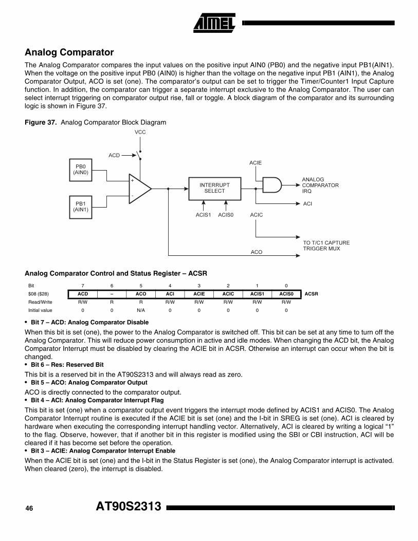
Analog ComparatorThe Analog Comparator compares the input values on the positive input AIN0 (PB0) and the negative input PB1(AIN1).When the voltage on the positive input PB0 (AIN0) is higher than the voltage on the negative input PB1 (AIN1), the AnalogComparator Output, ACO is set (one). The comparator’s output can be set to trigger the Timer/Counter1 Input Capturefunction. In addition, the comparator can trigger a separate interrupt exclusive to the Analog Comparator. The user canselect interrupt triggering on comparator output rise, fall or toggle. A block diagram of the comparator and its surroundinglogic is shown in Figure 37.
Figure 37. Analog Comparator Block Diagram
Analog Comparator Control and Status Register – ACSR
• Bit 7 – ACD: Analog Comparator Disable
When this bit is set (one), the power to the Analog Comparator is switched off. This bit can be set at any time to turn off theAnalog Comparator. This will reduce power consumption in active and idle modes. When changing the ACD bit, the AnalogComparator Interrupt must be disabled by clearing the ACIE bit in ACSR. Otherwise an interrupt can occur when the bit ischanged.• Bit 6 – Res: Reserved Bit
This bit is a reserved bit in the AT90S2313 and will always read as zero.• Bit 5 – ACO: Analog Comparator Output
ACO is directly connected to the comparator output.• Bit 4 – ACI: Analog Comparator Interrupt Flag
This bit is set (one) when a comparator output event triggers the interrupt mode defined by ACIS1 and ACIS0. The AnalogComparator Interrupt routine is executed if the ACIE bit is set (one) and the I-bit in SREG is set (one). ACI is cleared byhardware when executing the corresponding interrupt handling vector. Alternatively, ACI is cleared by writing a logical “1”to the flag. Observe, however, that if another bit in this register is modified using the SBI or CBI instruction, ACI will becleared if it has become set before the operation.• Bit 3 – ACIE: Analog Comparator Interrupt Enable
When the ACIE bit is set (one) and the I-bit in the Status Register is set (one), the Analog Comparator interrupt is activated.When cleared (zero), the interrupt is disabled.
Bit 7 6 5 4 3 2 1 0
$08 ($28) ACD – ACO ACI ACIE ACIC ACIS1 ACIS0 ACSR
Read/Write R/W R R R/W R/W R/W R/W R/W
Initial value 0 0 N/A 0 0 0 0 0
AT90S231346

AT90S2313
• Bit 2 – ACIC: Analog Comparator Input Capture Enable
When set (one), this bit enables the Input Capture function in Timer/Counter1 to be triggered by the Analog Comparator.The comparator output is, in this case, directly connected to the Input Capture front-end logic, making the comparator uti-lize the noise canceler and edge-select features of the Timer/Counter1 Input Capture interrupt. When cleared (zero), noconnection between the Analog Comparator and the Input Capture function is given. To make the comparator trigger theTimer/Counter1 Input Capture interrupt, the TICIE1 bit in the Timer Interrupt Mask Register (TIMSK) must be set (one).• Bits 1,0 – ACIS1, ACIS0: Analog Comparator Interrupt Mode Select
These bits determine which comparator events trigger the Analog Comparator interrupt. The different settings are shown inTable 16.
Note: When changing the ACIS1/ACIS0 bits, the Analog Comparator Interrupt must be disabled by clearing its Interrupt Enable bit in the ACSR register. Otherwise an interrupt can occur when the bits are changed.
I/O PortsAll AVR ports have true read-modify-write functionality when used as general digital I/O ports. This means that the directionof one port pin can be changed without unintentionally changing the direction of any other pin with the SBI and CBI instruc-tions. The same applies for changing drive value (if configured as output) or enabling/disabling of pull-up resistors (ifconfigured as input).
Port BPort B is an 8-bit bi-directional I/O port.
Three I/O memory address locations are allocated for the Port B, one each for the Data Register – PORTB, $18 ($38), DataDirection Register – DDRB, $17($37) and the Port B Input Pins – PINB, $16($36). The Port B Input Pins address is read-only, while the Data Register and the Data Direction Register are read/write.
All port pins have individually selectable pull-up resistors. The Port B output buffers can sink 20 mA and thus drive LED dis-plays directly. When pins PB0 to PB7 are used as inputs and are externally pulled low, they will source current if theinternal pull-up resistors are activated.
The Port B pins with alternate functions are shown in Table 17.
When the pins are used for the alternate function, the DDRB and PORTB registers have to be set according to the alternatefunction description.
Table 16. ACIS1/ACIS0 Settings
ACIS1 ACIS0 Interrupt Mode
0 0 Comparator Interrupt on Output Toggle
0 1 Reserved
1 0 Comparator Interrupt on Falling Output Edge
1 1 Comparator Interrupt on Rising Output Edge
Table 17. Port B Pin Alternate Functions
Port Pin Alternate Functions
PB0 AIN0 (Analog comparator positive input)
PB1 AIN1 (Analog comparator negative input)
PB3 OC1 (Timer/Counter1 Output compare match output)
PB5 MOSI (Data input line for memory downloading)
PB6 MISO (Data output line for memory uploading)
PB7 SCK (Serial clock input)
47
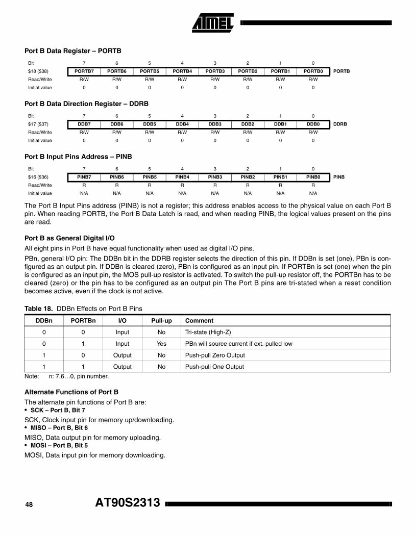
Port B Data Register – PORTB
Port B Data Direction Register – DDRB
Port B Input Pins Address – PINB
The Port B Input Pins address (PINB) is not a register; this address enables access to the physical value on each Port Bpin. When reading PORTB, the Port B Data Latch is read, and when reading PINB, the logical values present on the pinsare read.
Port B as General Digital I/O
All eight pins in Port B have equal functionality when used as digital I/O pins.
PBn, general I/O pin: The DDBn bit in the DDRB register selects the direction of this pin. If DDBn is set (one), PBn is con-figured as an output pin. If DDBn is cleared (zero), PBn is configured as an input pin. If PORTBn is set (one) when the pinis configured as an input pin, the MOS pull-up resistor is activated. To switch the pull-up resistor off, the PORTBn has to becleared (zero) or the pin has to be configured as an output pin The Port B pins are tri-stated when a reset conditionbecomes active, even if the clock is not active.
Note: n: 7,6…0, pin number.
Alternate Functions of Port B
The alternate pin functions of Port B are:• SCK – Port B, Bit 7
SCK, Clock input pin for memory up/downloading.• MISO – Port B, Bit 6
MISO, Data output pin for memory uploading.• MOSI – Port B, Bit 5
MOSI, Data input pin for memory downloading.
Bit 7 6 5 4 3 2 1 0
$18 ($38) PORTB7 PORTB6 PORTB5 PORTB4 PORTB3 PORTB2 PORTB1 PORTB0 PORTB
Read/Write R/W R/W R/W R/W R/W R/W R/W R/W
Initial value 0 0 0 0 0 0 0 0
Bit 7 6 5 4 3 2 1 0
$17 ($37) DDB7 DDB6 DDB5 DDB4 DDB3 DDB2 DDB1 DDB0 DDRB
Read/Write R/W R/W R/W R/W R/W R/W R/W R/W
Initial value 0 0 0 0 0 0 0 0
Bit 7 6 5 4 3 2 1 0
$16 ($36) PINB7 PINB6 PINB5 PINB4 PINB3 PINB2 PINB1 PINB0 PINB
Read/Write R R R R R R R R
Initial value N/A N/A N/A N/A N/A N/A N/A N/A
Table 18. DDBn Effects on Port B Pins
DDBn PORTBn I/O Pull-up Comment
0 0 Input No Tri-state (High-Z)
0 1 Input Yes PBn will source current if ext. pulled low
1 0 Output No Push-pull Zero Output
1 1 Output No Push-pull One Output
AT90S231348

AT90S2313
• OC1 – Port B, Bit 3
OC1, Output Compare Match Output. The PB3 pin can serve as an external output for timer 1 compare match. The PB3 pinhas to be configured as an output (DDB3 is set [one]) to serve this function. See the timer description for further details, andhow to enable the output.• AIN1 – Port B, Bit 1
AIN1, Analog Comparator Negative Input. When configured as an input (DDB1 is cleared [zero]) and with the internal MOSpull-up resistor switched off (PB1 is cleared [zero]), this pin also serves as the negative input of the on-chip AnalogComparator.• AIN0 – Port B, Bit 0
AIN0, Analog Comparator Positive Input. When configured as an input (DDB0 is cleared [zero]) and with the internal MOSpull-up resistor switched off (PB0 is cleared [zero]), this pin also serves as the positive input of the on-chip AnalogComparator.
Port B Schematics
Note that all port pins are synchronized. The synchronization latches are, however, not shown in the figures.
Figure 38. Port B Schematic Diagram (Pins PB0 and PB1)
49

Figure 39. Port B Schematic Diagram (Pin PB3)
Figure 40. Port B Schematic Diagram (Pins PB2 and PB4)
PB3
DDB3
MOSPULL-UP
RESET
RQ D
C
RD
WD
WP
COM1A0COM1A1
COMP. MATCH1OUTPUTMODE SELECT
RESET
RQ D
C
PORTB3
RL
RP
WP: WRITE PORTBWD: WRITE DDRBRL: READ PORTB LATCHRP: READ PORTB PINRD: READ DDRB
DA
TA
BU
S
AT90S231350

AT90S2313
Figure 41. Port B Schematic Diagram (Pin PB5)
Figure 42. Port B Schematic Diagram (Pin PB6)
51

Figure 43. Port B Schematic Diagram (Pin PB7)
Port DThree I/O memory address locations are allocated for the Port D: one each for the Data Register – PORTD, $12($32), DataDirection Register – DDRD, $11($31) and the Port D Input Pins – PIND, $10($30). The Port D Input Pins address is read-only, while the Data Register and the Data Direction Register are read/write.
Port D has seven bi-directional I/O pins with internal pull-up resistors, PD6..PD0. The Port D output buffers can sink 20 mA.As inputs, Port D pins that are externally pulled low will source current if the pull-up resistors are activated.
Some Port D pins have alternate functions as shown in Table 19:
When the pins are used for the alternate function, the DDRD and PORTD registers have to be set according to the alter-nate function description.
Table 19. Port D Pin Alternate Functions
Port Pin Alternate Function
PD0 RXD (Receive data input for the UART)
PD1 TXD (Transmit data output for the UART)
PD2 INT0 (External interrupt 0 input)
PD3 INT1 (External interrupt 1 input)
PD4 TO (Timer/Counter0 external input)
PD5 T1 (Timer/Counter1 external input)
PD6 ICP (Timer/Counter1Input Capture pin)
AT90S231352

AT90S2313
Port D Data Register – PORTD
Port D Data Direction Register – DDRD
Port D Input Pins Address – PIND
The Port D Input Pins address (PIND) is not a register; this address enables access to the physical value on each Port Dpin. When reading PORTD, the Port D Data Latch is read, and when reading PIND, the logical values present on the pinsare read.
Port D as General Digital I/O
PDn, general I/O pin: The DDDn bit in the DDRD register selects the direction of this pin. If DDDn is set (one), PDn is con-figured as an output pin. If DDDn is cleared (zero), PDn is configured as an input pin. If PORTDn is set (one) whenconfigured as an input pin, the MOS pull-up resistor is activated. To switch the pull-up resistor off, the PORTDn has to becleared (zero) or the pin has to be configured as an output pin. The Port D pins are tri-stated when a reset conditionbecomes active, even if the clock is not active.
Note: n: 6…0, pin number.
Alternate Functions of Port D
The alternate functions of Port D are:• ICP – Port D, Bit 6
Timer/Counter1 Input Capture pin. See the Timer/Counter1 description for further details.• T1 – Port D, Bit 5
T1, Timer 1 clock source. See the Timer description for further details.• T0 – Port D, Bit 4
T0, Timer/Counter0 clock source. See the Timer description for further details.• INT1 – Port D, Bit 3
INT1, External Interrupt Source 1. The PD3 pin can serve as an external interrupt source to the MCU. See the interruptdescription for further details and how to enable the source.
Bit 7 6 5 4 3 2 1 0
$12 ($32) – PORTD6 PORTD5 PORTD4 PORTD3 PORTD2 PORTD1 PORTD0 PORTD
Read/Write R R/W R/W R/W R/W R/W R/W R/W
Initial value 0 0 0 0 0 0 0 0
Bit 7 6 5 4 3 2 1 0
$11 ($31) – DDD6 DDD5 DDD4 DDD3 DDD2 DDD1 DDD0 DDRD
Read/Write R R/W R/W R/W R/W R/W R/W R/W
Initial value 0 0 0 0 0 0 0 0
Bit 7 6 5 4 3 2 1 0
$10 ($30) – PIND6 PIND5 PIND4 PIND3 PIND2 PIND1 PIND0 PIND
Read/Write R R R R R R R R
Initial value 0 N/A N/A N/A N/A N/A N/A N/A
Table 20. DDDn Bits on Port D Pins
DDDn PORTDn I/O Pull-up Comment
0 0 Input No Tri-state (High-Z)
0 1 Input Yes PDn will source current if ext. pulled low
1 0 Output No Push-pull Zero Output
1 1 Output No Push-pull One Output
53

• INT0 – Port D, Bit 2
INT0, External Interrupt Source 0. The PD2 pin can serve as an external interrupt source to the MCU. See the interruptdescription for further details and how to enable the source.• TXD – Port D, Bit 1
Transmit Data (Data output pin for the UART). When the UART transmitter is enabled, this pin is configured as an outputregardless of the value of DDRD1.• RXD – Port D, Bit 0
Receive Data (Data input pin for the UART). When the UART receiver is enabled, this pin is configured as an input regard-less of the value of DDRD0. When the UART forces this pin to be an input, a logical “1” in PORTD0 will turn on the internalpull-up.
Port D Schematics
Note that all port pins are synchronized. The synchronization latches are, however, not shown in the figures.
Figure 44. Port D Schematic Diagram (Pin PD0)
DA
TA B
US
D
D
Q
Q
RESET
RESET
C
C
WD
WP
RD
MOSPULL-UP
PD0
RXD
RXENWP:WD:RL:RP:RD:RXD:RXEN:
WRITE PORTDWRITE DDRDREAD PORTD LATCHREAD PORTD PINREAD DDRDUART RECEIVE DATAUART RECEIVE ENABLE
DDD0
PORTD0
RL
RP
AT90S231354
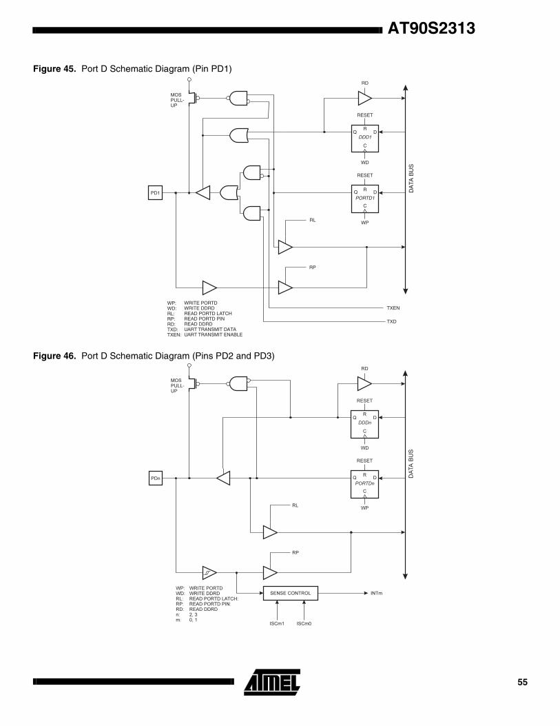
AT90S2313
Figure 45. Port D Schematic Diagram (Pin PD1)
Figure 46. Port D Schematic Diagram (Pins PD2 and PD3)
DA
TA B
US
D
D
Q
Q
RESET
RESET
C
C
WD
WP
RD
RP
RL
MOSPULL-UP
PD1
R
R
WP:WD:RL:RP:RD:TXD:TXEN:
WRITE PORTDWRITE DDRDREAD PORTD LATCHREAD PORTD PINREAD DDRDUART TRANSMIT DATAUART TRANSMIT ENABLE
DDD1
PORTD1
TXEN
TXD
55

Figure 47. Port D Schematic Diagram (Pins PD4 and PD5)
Figure 48. Port D Schematic Diagram (Pin PD6)
DA
TA B
US
D
D
Q
Q
RESET
RESET
C
C
WD
WP
RD
MOSPULL-UP
PDn
R
R
WP:WD:RL:RP:RD:n:m:
WRITE PORTDWRITE DDRDREAD PORTD LATCHREAD PORTD PINREAD DDRD4, 50, 1
DDDn
PORTDn
SENSE CONTROL TIMERm CLOCKSOURCE MUX
CSm2 CSm0
RL
RP
CSm1
AT90S231356

AT90S2313
Memory Programming
Program and Data Memory Lock BitsThe AT90S2313 MCU provides two Lock bits that can be left unprogrammed (“1”) or can be programmed (“0”) to obtain theadditional features listed in Table 21. The Lock bits can only be erased with the Chip Erase operation.
Note: 1. In the Parallel mode, further programming of the Fuse bits are also disabled. Program the Fuse bits before programming the Lock bits.
Fuse BitsThe AT90S2313 has two Fuse bits: SPIEN and FSTRT.• When the SPIEN Fuse is programmed (“0”), Serial Program and Data Downloading is enabled. The default value is
programmed (“0”).
• When the FSTRT Fuse is programmed (“0”), the short start-up time is selected. The default value is unprogrammed (“1”). Parts with this bit pre-programmed (“0”) can be delivered on demand.
The Fuse bits are not accessible in Serial Programming Mode. The status of the Fuses are not affected by Chip Erase.
Signature BytesAll Atmel microcontrollers have a 3-byte signature code that identifies the device. This code can be read in both serial andparallel mode. The three bytes reside in a separate address space.
For the AT90S2313(1) they are:
1. $000: $1E (indicates manufactured by Atmel)
2. $001: $91 (indicates 2 Kb Flash memory)
3. $002: $01 (indicates AT90S2313 device when signature byte $001 is $91)Note: 1. When both Lock bits are programmed (Lock mode 3), the signature bytes cannot be read in serial mode. Reading the signa-
ture bytes will return: $00, $01 and $02.
Programming the Flash and EEPROMAtmel’s AT90S2313 offers 2K bytes of in-system reprogrammable Flash program memory and 128 bytes of EEPROM datamemory.
The AT90S2313 is shipped with the on-chip Flash program and EEPROM data memory arrays in the erased state(i.e., contents = $FF) and ready to be programmed. This device supports a high-voltage (12V) Parallel Programming Modeand a low-voltage Serial Programming Mode. The +12V is used for programming enable only, and no current of signifi-cance is drawn by this pin. The Serial Programming Mode provides a convenient way to download program and data intothe AT90S2313 inside the user’s system.
The program and EEPROM memory arrays in the AT90S2313 are programmed byte-by-byte in either programming mode.For the EEPROM, an auto-erase cycle is provided within the self-timed write instruction in the Serial Programming Mode.During programming, the supply voltage must be in accordance with Table 22.
Table 21. Lock Bit Protection Modes
Memory Lock Bits
Protection TypeMode LB1 LB2
1 1 1 No memory lock features enabled.
2 0 1 Further programming of the Flash and EEPROM is disabled.(1)
3 0 0 Same as mode 2, and verify is also disabled.
57

Parallel ProgrammingThis section describes how to parallel program and verify Flash program memory, EEPROM data memory, Lock bits andFuse bits in the AT90S2313.
Signal Names
In this section, some pins of the AT90S2313 are referenced by signal names describing their function during parallelprogramming. Pins not described in the following table are referenced by pin names. See Figure 49 and Table 23. Pins notdescribed in Table 23 are referenced by pin names.
The XA1/XA0 pins determine the action executed when the XTAL1 pin is given a positive pulse. The bit coding is shown inTable 24.
When pulsing WR or OE, the command loaded determines the action executed. The command is a byte where thedifferent bits are assigned functions as shown in Table 25.
Figure 49. Parallel Programming
.
Table 22. Supply Voltage during Programming
Part Serial Programming Parallel Programming
AT90S2313 2.7 - 6.0V 4.5 - 5.5V
Table 23. Pin Name Mapping
Signal Name in Programming Mode Pin Name I/O Function
RDY/BSY PD1 O 0: Device is busy programming, 1: Device is ready for new command
OE PD2 I Output Enable (Active low)
WR PD3 I Write Pulse (Active low)
BS PD4 I Byte Select (“0” selects low byte, “1” selects high byte)
XA0 PD5 I XTAL Action Bit 0
XA1 PD6 I XTAL Action Bit 1
DATA PB7-0 I/O Bi-directional Data Bus (Output when OE is low)
AT90S231358
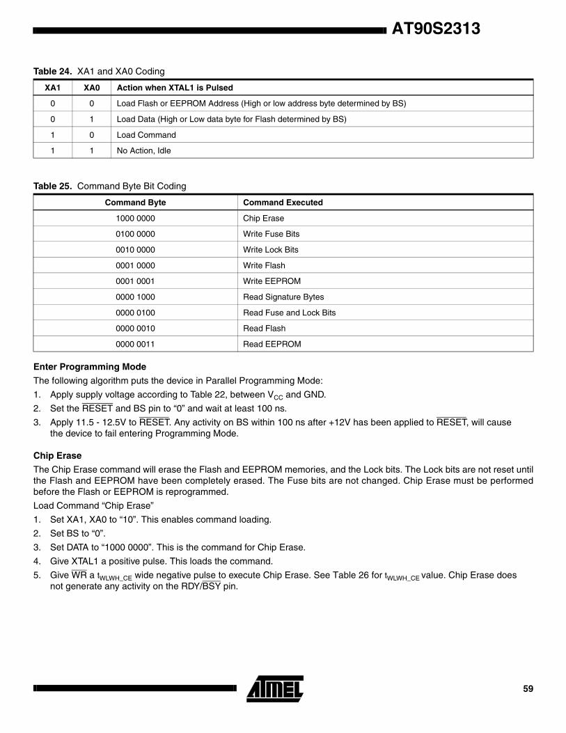
AT90S2313
Enter Programming Mode
The following algorithm puts the device in Parallel Programming Mode:
1. Apply supply voltage according to Table 22, between VCC and GND.
2. Set the RESET and BS pin to “0” and wait at least 100 ns.
3. Apply 11.5 - 12.5V to RESET. Any activity on BS within 100 ns after +12V has been applied to RESET, will cause the device to fail entering Programming Mode.
Chip Erase
The Chip Erase command will erase the Flash and EEPROM memories, and the Lock bits. The Lock bits are not reset untilthe Flash and EEPROM have been completely erased. The Fuse bits are not changed. Chip Erase must be performedbefore the Flash or EEPROM is reprogrammed.
Load Command “Chip Erase”
1. Set XA1, XA0 to “10”. This enables command loading.
2. Set BS to “0”.
3. Set DATA to “1000 0000”. This is the command for Chip Erase.
4. Give XTAL1 a positive pulse. This loads the command.
5. Give WR a tWLWH_CE wide negative pulse to execute Chip Erase. See Table 26 for tWLWH_CE value. Chip Erase does not generate any activity on the RDY/BSY pin.
Table 24. XA1 and XA0 Coding
XA1 XA0 Action when XTAL1 is Pulsed
0 0 Load Flash or EEPROM Address (High or low address byte determined by BS)
0 1 Load Data (High or Low data byte for Flash determined by BS)
1 0 Load Command
1 1 No Action, Idle
Table 25. Command Byte Bit Coding
Command Byte Command Executed
1000 0000 Chip Erase
0100 0000 Write Fuse Bits
0010 0000 Write Lock Bits
0001 0000 Write Flash
0001 0001 Write EEPROM
0000 1000 Read Signature Bytes
0000 0100 Read Fuse and Lock Bits
0000 0010 Read Flash
0000 0011 Read EEPROM
59

Programming the Flash
A: Load Command “Write Flash”
1. Set XA1, XA0 to “10”. This enables command loading.
2. Set BS to “0”.
3. Set DATA to “0001 0000”. This is the command for Write Flash.
4. Give XTAL1 a positive pulse. This loads the command.
B: Load Address High Byte
1. Set XA1, XA0 to “00”. This enables address loading.
2. Set BS to “1”. This selects high byte.
3. Set DATA = Address high byte ($00 - $03).
4. Give XTAL1 a positive pulse. This loads the address high byte.
C: Load Address Low Byte
1. Set XA1, XA0 to “00”. This enables address loading.
2. Set BS to “0”. This selects low byte.
3. Set DATA = Address low byte ($00 - $FF).
4. Give XTAL1 a positive pulse. This loads the address low byte.
D: Load Data Low Byte
1. Set XA1, XA0 to “01”. This enables data loading.
2. Set DATA = Data low byte ($00 - $FF).
3. Give XTAL1 a positive pulse. This loads the data low byte.
E: Write Data Low Byte
1. Set BS to “0”. This selects low data.
2. Give WR a negative pulse. This starts programming of the data byte. RDY/BSY goes low.
3. Wait until RDY/BSY goes high to program the next byte.
(See Figure 50 for signal waveforms.)
F: Load Data High Byte
1. Set XA1, XA0 to “01”. This enables data loading.
2. Set DATA = Data high byte ($00 - $FF).
3. Give XTAL1 a positive pulse. This loads the data high byte.
G: Write Data High Byte
1. Set BS to “1”. This selects high data.
2. Give WR a negative pulse. This starts programming of the data byte. RDY/BSY goes low.
3. Wait until RDY/BSY goes high to program the next byte.
(See Figure 51 for signal waveforms.)
The loaded command and address are retained in the device during programming. For efficient programming, the followingshould be considered:• The command needs only be loaded once when writing or reading multiple memory locations.
• Address high byte needs only be loaded before programming a new 256-word page in the Flash.
• Skip writing the data value $FF; that is, the contents of the entire Flash and EEPROM after a Chip Erase.
These considerations also apply to EEPROM programming and Flash, EEPROM and signature byte reading.
AT90S231360

AT90S2313
Figure 50. Programming the Flash
Figure 51. Programming the Flash (Continued)
$10 ADDR. HIGH ADDR. LOW DATA LOWDATA
XA1
XA0
BS
XTAL1
WR
RDY/BSY
RESET
OE
12V
DATA HIGHDATA
XA1
XA0
BS
XTAL1
WR
RDY/BSY
RESET +12V
OE
61
Reading the Flash
The algorithm for reading the Flash memory is as follows (refer to “Programming the Flash” for details on command andaddress loading):
1. A: Load Command “0000 0010”.
2. B: Load Address High Byte ($00 - $03).
3. C: Load Address Low Byte ($00 - $FF).
4. Set OE to “0”, and BS to “0”. The Flash word low byte can now be read at DATA.
5. Set BS to “1”. The Flash word high byte can now be read from DATA.
6. Set OE to “1”.
Programming the EEPROM
The programming algorithm for the EEPROM data memory is as follows (refer to “Programming the Flash” for details oncommand, address and data loading):
1. A: Load Command “0001 0001”.
2. C: Load Address Low Byte ($00 - $7F).
3. D: Load Data Low Byte ($00 - $FF).
4. E: Write Data Low Byte.
Reading the EEPROM
The algorithm for reading the EEPROM memory is as follows (refer to “Programming the Flash” for details on commandand address loading):
1. A: Load Command “0000 0011”.
2. C: Load Address Low Byte ($00 - $7F).
3. Set OE to “0”, and BS to “0”. The EEPROM data byte can now be read at DATA.
4. Set OE to “1”.
Programming the Fuse Bits
The algorithm for programming the Fuse bits is as follows (refer to “Programming the Flash” for details on command anddata loading):
1. A: Load Command “0100 0000”.
2. D: Load Data Low Byte. Bit n = “0” programs and bit n = “1” erases the Fuse bit.
Bit 5 = SPIEN Fuse bit.
Bit 0 = FSTRT Fuse bit.
Bit 7-6,4-1 = “1”. These bits are reserved and should be left unprogrammed (“1”).
3. Give WR a tWLWH_PFB wide negative pulse to execute the programming; tWLWH_PFB is found in Table 26. Programming the Fuse bits does not generate any activity on the RDY/BSY pin.
AT90S231362

AT90S2313
Programming the Lock Bits
The algorithm for programming the Lock bits is as follows (refer to “Programming the Flash” on page 60 for details on com-mand and data loading):
1. A: Load Command “0010 0000”.
2. D: Load Data Low Byte. Bit n = “0” programs the Lock bit.
Bit 2 = Lock Bit2
Bit 1 = Lock Bit1
Bit 7-3,0 = “1”. These bits are reserved and should be left unprogrammed (“1”).
3. E: Write Data Low Byte.
The Lock bits can only be cleared by executing Chip Erase.
Reading the Fuse and Lock Bits
The algorithm for reading the Fuse and Lock bits is as follows (refer to “Programming the Flash” on page 60 for details oncommand loading):
1. A: Load Command “0000 0100”.
2. Set OE to “0”, and BS to “1”. The status of the Fuse and Lock bits can now be read at DATA (“0” means programmed).
Bit 7 = Lock Bit1
Bit 6 = Lock Bit2
Bit 5 = SPIEN Fuse bit
Bit 0 = FSTRT Fuse bit
3. Set OE to “1”.
Observe that BS needs to be set to “1”.
Reading the Signature Bytes
The algorithm for reading the signature bytes is as follows (refer to “Programming the Flash” on page 60 for details on com-mand and address loading):
1. A: Load Command “0000 1000”.
2. C: Load Address Low Byte ($00 - $02).
Set OE to “0”, and BS to “0”. The selected signature byte can now be read at DATA.
3. Set OE to “1”.
63

Parallel Programming Characteristics
Figure 52. Parallel Programming Timing
Notes: 1. Use tWLWH_CE for chip erase and tWLWH_PFB for programming the Fuse bits.2. If tWLWH is held longer than tWLRH, no RDY/BSY pulse will be seen.
Table 26. Parallel Programming Characteristics, TA = 25°C ± 10%, VCC = 5V ± 10%
Symbol Parameter Min Typ Max Units
VPP Programming Enable Voltage 11.5 12.5 V
IPP Programming Enable Current 250.0 µA
tDVXH Data and Control Setup before XTAL1 High 67.0 ns
tXHXL XTAL1 Pulse Width High 67.0 ns
tXLDX Data and Control Hold after XTAL1 Low 67.0 ns
tXLWL XTAL1 Low to WR Low 67.0 ns
tBVWL BS Valid to WR Low 67.0 ns
tRHBX BS Hold after RDY/BSY High 67.0 ns
tWLWH WR Pulse Width Low(1) 67.0 ns
tWHRL WR High to RDY/BSY Low(2) 20.0 ns
tWLRH WR Low to RDY/BSY High(2) 0.5 0.7 0.9 ms
tXLOL XTAL1 Low to OE Low 67.0 ns
tOLDV OE Low to DATA Valid 20.0 ns
tOHDZ OE High to DATA Tri-stated 20.0 ns
tWLWH_CE WR Pulse Width Low for Chip Erase 5.0 10.0 15.0 ms
tWLWH_PFB WR Pulse Width Low for Programming the Fuse Bits 1.0 1.5 1.8 ms
Data & Contol(DATA, XA0/1, BS)
DATA
Writ
eR
ead
XTAL1 tXHXL
tWLWH
tDVXH
tXLOL tOLDV
tWHRL
tWLRH
WR
RDY/BSY
OE
tXLDX
tXLWL
tRHBX
tOHDZ
tBVWL
AT90S231364
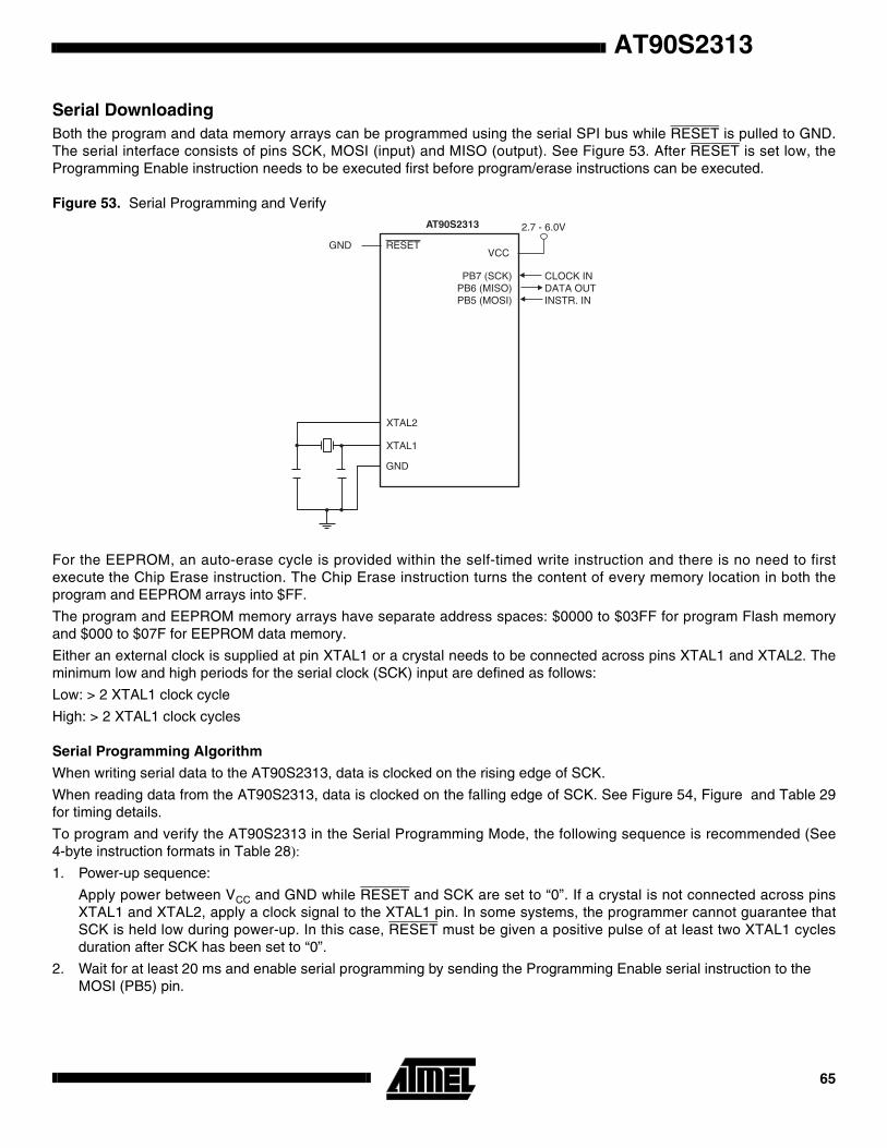
AT90S2313
Serial DownloadingBoth the program and data memory arrays can be programmed using the serial SPI bus while RESET is pulled to GND.The serial interface consists of pins SCK, MOSI (input) and MISO (output). See Figure 53. After RESET is set low, theProgramming Enable instruction needs to be executed first before program/erase instructions can be executed.
Figure 53. Serial Programming and Verify
For the EEPROM, an auto-erase cycle is provided within the self-timed write instruction and there is no need to firstexecute the Chip Erase instruction. The Chip Erase instruction turns the content of every memory location in both theprogram and EEPROM arrays into $FF.
The program and EEPROM memory arrays have separate address spaces: $0000 to $03FF for program Flash memoryand $000 to $07F for EEPROM data memory.
Either an external clock is supplied at pin XTAL1 or a crystal needs to be connected across pins XTAL1 and XTAL2. Theminimum low and high periods for the serial clock (SCK) input are defined as follows:
Low: > 2 XTAL1 clock cycle
High: > 2 XTAL1 clock cycles
Serial Programming Algorithm
When writing serial data to the AT90S2313, data is clocked on the rising edge of SCK.
When reading data from the AT90S2313, data is clocked on the falling edge of SCK. See Figure 54, Figure and Table 29for timing details.
To program and verify the AT90S2313 in the Serial Programming Mode, the following sequence is recommended (See4-byte instruction formats in Table 28):1. Power-up sequence:
Apply power between VCC and GND while RESET and SCK are set to “0”. If a crystal is not connected across pinsXTAL1 and XTAL2, apply a clock signal to the XTAL1 pin. In some systems, the programmer cannot guarantee thatSCK is held low during power-up. In this case, RESET must be given a positive pulse of at least two XTAL1 cyclesduration after SCK has been set to “0”.
2. Wait for at least 20 ms and enable serial programming by sending the Programming Enable serial instruction to the MOSI (PB5) pin.
AT90S2313
VCC
2.7 - 6.0V
PB7 (SCK)PB6 (MISO)PB5 (MOSI)
RESET
GND
XTAL1
GND
CLOCK INDATA OUTINSTR. IN
XTAL2
65

3. The serial programming instructions will not work if the communication is out of synchronization. When in sync, the second byte ($53) will echo back when issuing the third byte of the Programming Enable instruction. Whether the echo is correct or not, all four bytes of the instruction must be transmitted. If the $53 did not echo back, give SCK a positive pulse and issue a new Programming Enable instruction. If the $53 is not seen within 32 attempts, there is no functional device connected.
4. If a Chip Erase is performed (must be done to erase the Flash), wait tWD_ERASE after the instruction, give RESET a positive pulse, and start over from step 2. See Table 30 for tWD_ERASE value.
5. The Flash or EEPROM array is programmed one byte at a time by supplying the address and data together with the appropriate Write instruction. An EEPROM memory location is first automatically erased before new data is written. Use Data Polling to detect when the next byte in the Flash or EEPROM can be written. If polling is not used, wait tWD_PROG before transmitting the next instruction. See Table 31 for tWD_PROG value. In an erased device, no $FFs in the data file(s) need to be programmed.
6. Any memory location can be verified by using the Read instruction that returns the content at the selected address at the serial output MISO (PB6) pin.
7. At the end of the programming session, RESET can be set high to commence normal operation.
8. Power-off sequence (if needed):
Set XTAL1 to “0” (if a crystal is not used).
Set RESET to “1”.
Turn VCC power off.
Data Polling EEPROM
When a byte is being programmed into the EEPROM, reading the address location being programmed will give the valueP1 until the auto-erase is finished, and then the value P2. See Table 27 for P1 and P2 values.
At the time the device is ready for a new EEPROM byte, the programmed value will read correctly. This is used to deter-mine when the next byte can be written. This will not work for the values P1 and P2, so when programming these values,the user will have to wait for at least the prescribed time tWD_PROG before programming the next byte. See Table 30 fortWD_PROG value. As a chip-erased device contains $FF in all locations, programming of addresses that are meant to contain$FF can be skipped. This does not apply if the EEPROM is reprogrammed without first chip-erasing the device.
Data Polling Flash
When a byte is being programmed into the Flash, reading the address location being programmed will give the value $7F.At the time the device is ready for a new byte, the programmed value will read correctly. This is used to determine when thenext byte can be written. This will not work for the value $7F, so when programming this value, the user will have to wait forat least tWD_PROG before programming the next byte. As a chip-erased device contains $FF in all locations, programming ofaddresses that are meant to contain $FF can be skipped.
Figure 54. Serial Programming Waveforms
Table 27. Read Back Value during EEPROM Polling
Part P1 P2
AT90S2313 $80 $7F
AT90S231366

AT90S2313
Note: a = address high bitsb = address low bitsH = 0 – Low byte, 1 – High Byteo = data outi = data inx = don’t care1 = Lock bit 12 = Lock bit 2
Note: 1. The signature bytes are not readable in lock mode 3, i.e. both Lock bits programmed.
Table 28. Serial Programming Instruction Set
Instruction
Instruction Format
OperationByte 1 Byte 2 Byte 3 Byte4
Programming Enable1010 1100 0101 0011 xxxx xxxx xxxx xxxx Enable serial programming while
RESET is low.
Chip Erase1010 1100 100x xxxx xxxx xxxx xxxx xxxx Chip erase Flash and EEPROM
memory arrays.
Read Program Memory0010 H000 xxxx xxaa bbbb bbbb oooo oooo Read H (high or low) data o from
program memory at word address a:b.
Write Program Memory0100 H000 xxxx xxaa bbbb bbbb iiii iiii Write H (high or low) data i to
program memory at word address a:b.
Read EEPROM Memory
1010 0000 xxxx xxxx xbbb bbbb oooo oooo Read data o from EEPROM memory at address b.
Write EEPROM Memory
1100 0000 xxxx xxxx xbbb bbbb iiii iiii Write data i to EEPROM memory at address b.
Write Lock Bits1010 1100 111x x21x xxxx xxxx xxxx xxxx Write Lock bits. Set bits 1,2 = “0” to
program Lock bits.
Read Signature Bytes 0011 0000 xxxx xxxx xxxx xxbb oooo oooo Read signature byte o at address b.(1)
67
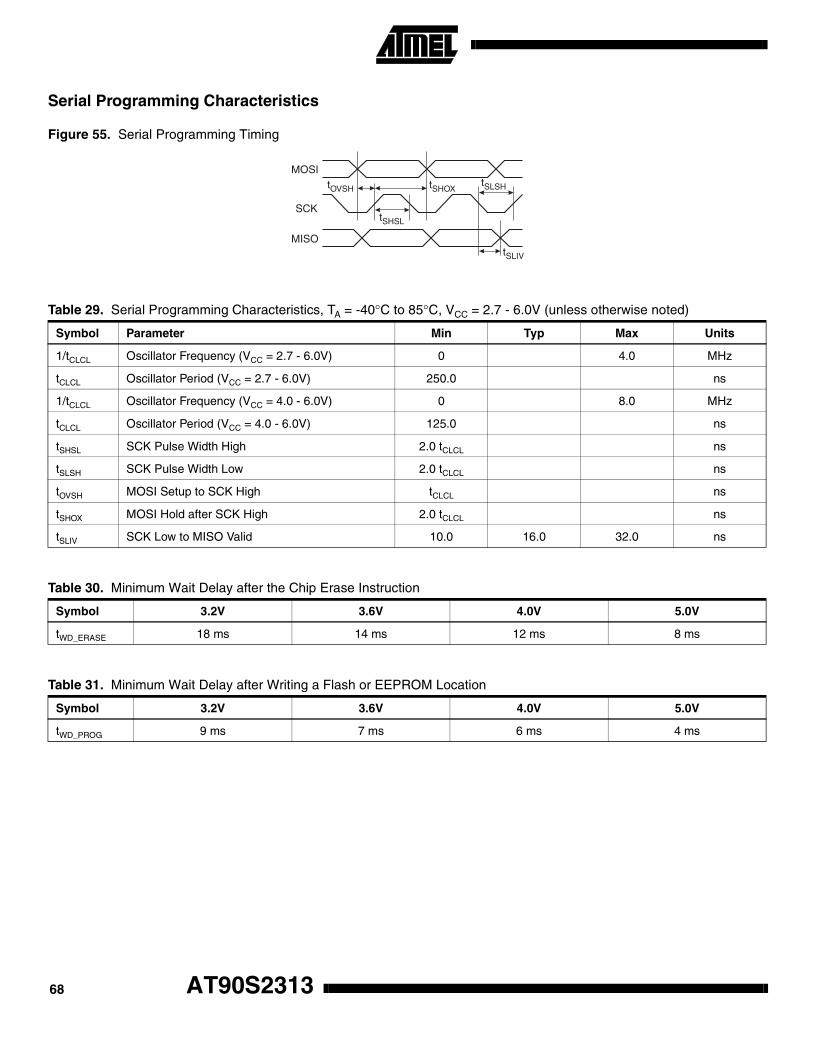
Serial Programming Characteristics
Figure 55. Serial Programming Timing
Table 29. Serial Programming Characteristics, TA = -40°C to 85°C, VCC = 2.7 - 6.0V (unless otherwise noted)
Symbol Parameter Min Typ Max Units
1/tCLCL Oscillator Frequency (VCC = 2.7 - 6.0V) 0 4.0 MHz
tCLCL Oscillator Period (VCC = 2.7 - 6.0V) 250.0 ns
1/tCLCL Oscillator Frequency (VCC = 4.0 - 6.0V) 0 8.0 MHz
tCLCL Oscillator Period (VCC = 4.0 - 6.0V) 125.0 ns
tSHSL SCK Pulse Width High 2.0 tCLCL ns
tSLSH SCK Pulse Width Low 2.0 tCLCL ns
tOVSH MOSI Setup to SCK High tCLCL ns
tSHOX MOSI Hold after SCK High 2.0 tCLCL ns
tSLIV SCK Low to MISO Valid 10.0 16.0 32.0 ns
Table 30. Minimum Wait Delay after the Chip Erase Instruction
Symbol 3.2V 3.6V 4.0V 5.0V
tWD_ERASE 18 ms 14 ms 12 ms 8 ms
Table 31. Minimum Wait Delay after Writing a Flash or EEPROM Location
Symbol 3.2V 3.6V 4.0V 5.0V
tWD_PROG 9 ms 7 ms 6 ms 4 ms
MOSI
MISO
SCK
tOVSH
tSHSL
tSLSHtSHOX
tSLIV
AT90S231368

AT90S2313
Electrical Characteristics
Absolute Maximum Ratings*Operating Temperature.................................. -55°C to +125°C *NOTICE: Stresses beyond those listed under “Absolute
Maximum Ratings” may cause permanent dam-age to the device. This is a stress rating only and functional operation of the device at these or other conditions beyond those indicated in the operational sections of this specification is not implied. Exposure to absolute maximum rating conditions for extended periods may affect device reliability.
Storage Temperature ..................................... -65°C to +150°C
Voltage on Any Pin Except RESETwith Respect to Ground ...............................-1.0V to VCC+0.5V
Voltage on RESET with Respect to Ground ....-1.0V to +13.0V
Maximum Operating Voltage ............................................ 6.6V
DC Current per I/O Pin ............................................... 40.0 mA
DC Current VCC and GND Pins ................................ 200.0 mA
69

Notes: 1. “Max” means the highest value where the pin is guaranteed to be read as low.2. “Min” means the lowest value where the pin is guaranteed to be read as high.3. Although each I/O port can sink more than the test conditions (20 mA at VCC = 5V, 10 mA at VCC = 3V) under steady state
conditions (non-transient), the following must be observed:1] The sum of all IOL, for all ports, should not exceed 200 mA2] The sum of all IIOL, for port D0 - D5 and XTAL2 should not exceed 100 mA.3] The sum of all IOL, for ports B0 - B7 and D6 should not exceed 100 mA.If IOL exceeds the test condition, VOL may exceed the related specification. Pins are not guaranteed to sink current greater than the listed test condition.
4. Although each I/O port can source more than the test conditions (3 mA at VCC = 5V, 1.5 mA at VCC = 3V) under steady state conditions (non-transient), the following must be observed:1] The sum of all IOH, for all ports, should not exceed 200 mA2] The sum of all IOH, for port D0 - D5 and XTAL2 should not exceed 100 mA.3] The sum of all IOH, for ports B0 - B7 and D6 should not exceed 100 mA.If IOH exceeds the test condition, VOH may exceed the related specification. Pins are not guaranteed to source current greater than the listed test condition.
5. Minimum VCC for power-down is 2V.
DC CharacteristicsTA = -40°C to 85°C, VCC = 2.7V to 6.0V (unless otherwise noted)
Symbol Parameter Condition Min Typ Max Units
VIL Input Low Voltage (Except XTAL1) -0.5 0.3 VCC(1) V
VIL1 Input Low Voltage (XTAL1) -0.5 0.3 VCC(1) V
VIH Input High Voltage (Except XTAL1, RESET) 0.6 VCC(2) VCC + 0.5 V
VIH1 Input High Voltage (XTAL1) 0.7 VCC(2) VCC + 0.5 V
VIH2 Input High Voltage (RESET) 0.85 VCC(2) VCC + 0.5 V
VOLOutput Low Voltage(3)
(Ports B, D)IOL = 20 mA, VCC = 5VIOL = 10 mA, VCC = 3V
0.60.5
VV
VOHOutput High Voltage(4)
(Ports B, D)IOH = -3 mA, VCC = 5VIOH = -1.5 mA, VCC = 3V
4.32.3
VV
IILInput LeakageCurrent I/O pin
VCC = 6V, pin low (absolute value)
1.5 µA
IIHInput LeakageCurrent I/O pin
VCC = 6V, pin high(absolute value)
980.0 nA
RRST Reset Pull-up Resistor 100.0 500.0 kΩ
RI/O I/O Pin Pull-up Resistor 35.0 120.0 kΩ
ICC Power Supply CurrentActive Mode, VCC = 3V, 4 MHz 3.0 mA
Idle Mode VCC = 3V, 4 MHz 1.0 mA
ICC Power-down Mode(5)WDT enabled, VCC = 3V 9.0 15.0 µA
WDT disabled, VCC = 3V <1.0 2.0 µA
VACIOAnalog Comparator Input Offset Voltage
VCC = 5VVin = VCC /2
40.0 mV
IACLKAnalog Comparator Input Leakage Current
VCC = 5VVin = VCC/2
-50.0 50.0 nA
tACPDAnalog Comparator Propagation Delay
VCC = 2.7VVCC = 4.0V
750.0500.0
ns
AT90S231370

AT90S2313
External Clock Drive Waveforms
Figure 56. External Clock
External Clock Drive
Symbol Parameter
VCC = 2.7V to 6.0V VCC = 4.0V to 6.0V
UnitsMin Max Min Max
1/tCLCL Oscillator Frequency 0 4 0 10.0 MHz
tCLCL Clock Period 250.0 100.0 ns
tCHCX High Time 100.0 40.0 ns
tCLCX Low Time 100.0 40.0 ns
tCLCH Rise Time 1.6 0.5 µs
tCHCL Fall Time 1.6 0.5 µs
VIL1
VIH1
71

Typical CharacteristicsThe following charts show typical behavior. These figures are not tested during manufacturing. All current consumptionmeasurements are performed with all I/O pins configured as inputs and with internal pull-ups enabled. A sine wave genera-tor with rail-to-rail output is used as clock source.
The power consumption in Power-Down Mode is independent of clock selection.
The current consumption is a function of several factors such as: operating voltage, operating frequency, loading of I/Opins, switching rate of I/O pins, code executed and ambient temperature. The dominating factors are operating voltage andfrequency.
The current drawn from capacitive loaded pins may be estimated (for one pin) as CL • VCC • f where CL = load capacitance,VCC = operating voltage and f = average switching frequency of I/O pin.
The parts are characterized at frequencies higher than test limits. Parts are not guaranteed to function properly at frequen-cies higher than the ordering code indicates.
The difference between current consumption in Power-down Mode with Watchdog timer enabled and Power-down Modewith Watchdog timer disabled represents the differential current drawn by the Watchdog timer.
Figure 57. Active Supply Current vs. Frequency
0
5
10
15
20
25
0 1 2 3 4 5 6 7 8 9 10 11 12 13 14 15
ACTIVE SUPPLY CURRENT vs. FREQUENCYT = 25˚CA
Frequency (MHz)
Icc
(mA
)
Vcc = 5.5V
Vcc = 5V
Vcc= 2.7V
Vcc= 3.0VVcc = 3.3VVcc= 3.6VVcc= 4V
Vcc= 4.5V
Vcc = 6V
AT90S231372

AT90S2313
Figure 58. Active Supply Current vs. VCC
Figure 59. Idle Supply Current vs. Frequency
0
2
4
6
8
10
12
2 2.5 3 3.5 4 4.5 5 5.5 6
ACTIVE SUPPLY CURRENT vs. VccFREQUENCY = 4 MHz
Icc
(mA
)
Vcc(V)
T = 85˚CA
T = 25˚CA
0
1
2
3
4
5
6
7
8
0 1 2 3 4 5 6 7 8 9 10 11 12 13 14 15
Vcc= 6V
Vcc= 5.5V
Vcc= 5V
Vcc= 4.5V
Vcc= 4V
Vcc= 3.6VVcc= 3.3VVcc= 3.0V
Vcc= 2.7V
IDLE SUPPLY CURRENT vs. FREQUENCYT = 25˚CA
Frequency (MHz)
Icc
(mA
)
73

Figure 60. Idle Supply Current vs. VCC
Figure 61. Power-down Supply Current vs. VCC
IDLE SUPPLY CURRENT vs. VccI
cc (m
A)
Vcc(V)
FREQUENCY = 4 MHz
0
0.5
1
1.5
2
2.5
3
3.5
2 2.5 3 3.5 4 4.5 5 5.5 6
T = 25˚CA
T = 85˚CA
0
0.2
0.4
0.6
0.8
1
1.2
1.4
1.6
1.8
2
2 2.5 3 3.5 4 4.5 5 5.5 6
T = 85˚CA
T = 25˚CA
POWER DOWN SUPPLY CURRENT vs. Vcc
Icc
(µΑ
)
Vcc(V)
WATCHDOG TIMER DISABLED
T = 45˚CA
T = 70˚CA
AT90S231374

AT90S2313
Figure 62. Power-down Supply Current vs. VCC
Figure 63. Analog Comparator Current vs. VCC
Note: Analog Comparator offset voltage is measured as absolute offset.
0
20
40
60
80
100
120
140
160
2 2.5 3 3.5 4 4.5 5 5.5 6
T = 85˚CA
T = 25˚CA
POWER DOWN SUPPLY CURRENT vs. Vcc
Icc
(µΑ
)
Vcc(V)
WATCHDOG TIMER ENABLED
0
0.1
0.2
0.3
0.4
0.5
0.6
0.7
0.8
0.9
2 2.5 3 3.5 4 4.5 5 5.5 6
ANALOG COMPARATOR CURRENT vs. Vcc
Icc
(mA
)
Vcc(V)
T = 25˚CA
T = 85˚CA
75
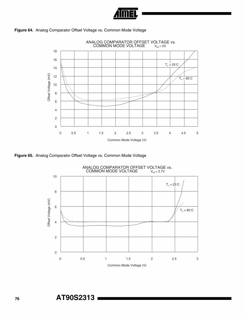
Figure 64. Analog Comparator Offset Voltage vs. Common Mode Voltage
Figure 65. Analog Comparator Offset Voltage vs. Common Mode Voltage
0
2
4
6
8
10
12
14
16
18
0 0.5 1 1.5 2 2.5 3 3.5 4 4.5 5
ANALOG COMPARATOR OFFSET VOLTAGE vs.V = 5VccCOMMON MODE VOLTAGE
Common Mode Voltage (V)
Offs
et V
olta
ge (
mV
)
T = 85˚CA
T = 25˚CA
0
2
4
6
8
10
0 0.5 1 1.5 2 2.5 3
ANALOG COMPARATOR OFFSET VOLTAGE vs.COMMON MODE VOLTAGE
Common Mode Voltage (V)
Offs
et V
olta
ge (
mV
)
V = 2.7Vcc
T = 85˚CA
T = 25˚CA
AT90S231376

AT90S2313
Figure 66. Analog Comparator Input Leakage Current
Figure 67. Watchdog Oscillator Frequency vs. VCC
Note: Sink and source capabilities of I/O ports are measured on one pin at a time.
60
50
40
30
20
10
0
-100 0.5 1.51 2 2.5 3.53 4 4.5 5 6 6.5 75.5
ANALOG COMPARATOR INPUT LEAKAGE CURRENTT = 25˚CA
I (
nA)
AC
LK
V (V)IN
V = 6VCC
0
200
400
600
800
1000
1200
1400
1600
2 2.5 3 3.5 4 4.5 5 5.5 6
T = 85˚CA
T = 25˚CA
WATCHDOG OSCILLATOR FREQUENCY vs. Vcc
V (V)cc
F (
KH
z)R
C
77
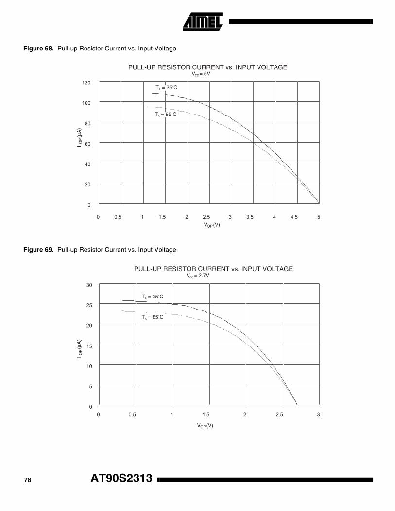
Figure 68. Pull-up Resistor Current vs. Input Voltage
Figure 69. Pull-up Resistor Current vs. Input Voltage
0
20
40
60
80
100
120
0 0.5 1 1.5 2 2.5 3 3.5 4 4.5 5
PULL-UP RESISTOR CURRENT vs. INPUT VOLTAGEV = 5Vcc
I (
µA)
OP
V (V)OP
T = 85˚CA
T = 25˚CA
0
5
10
15
20
25
30
0 0.5 1 1.5 2 2.5 3
PULL-UP RESISTOR CURRENT vs. INPUT VOLTAGE
I (
µA)
OP
V (V)OP
V = 2.7Vcc
T = 85˚CA
T = 25˚CA
AT90S231378

AT90S2313
Figure 70. I/O Pin Sink Current vs. Output Voltage
Figure 71. I/O Pin Source Current vs. Output Voltage
0
10
20
30
40
50
60
70
0 0.5 1 1.5 2 2.5 3
V = 5VccI
(m
A)
OL
V (V)OL
T = 85˚CA
T = 25˚CA
I/O PIN SINK CURRENT vs. OUTPUT VOLTAGE
0
2
4
6
8
10
12
14
16
18
20
0 0.5 1 1.5 2 2.5 3 3.5 4 4.5 5
I/O PIN SOURCE CURRENT vs. OUTPUT VOLTAGEV = 5Vcc
I (
mA
)O
H
V (V)OH
T = 85˚CA
T = 25˚CA
79

Figure 72. I/O Pin Sink Current vs. Output Voltage
Figure 73. I/O Pin Source Current vs. Output Voltage
0
5
10
15
20
25
0 0.5 1 1.5 2
I (
mA
)O
L
V (V)OL
T = 85˚CA
T = 25˚CA
I/O PIN SINK CURRENT vs. OUTPUT VOLTAGEV = 2.7Vcc
0
1
2
3
4
5
6
0 0.5 1 1.5 2 2.5 3
I/O PIN SOURCE CURRENT vs. OUTPUT VOLTAGE
I (
mA
)O
H
V (V)OH
T = 85˚CA
T = 25˚CA
V = 2.7Vcc
AT90S231380

AT90S2313
Figure 74. I/O Pin Input Threshold Voltage vs. VCC
Figure 75. I/O Pin Input Hysteresis vs. VCC
0
0.5
1
1.5
2
2.5
2.7 4.0 5.0
Thr
esho
ld V
olta
ge (
V)
V cc
I/O PIN INPUT THRESHOLD VOLTAGE vs. VccT = 25˚CA
0
0.02
0.04
0.06
0.08
0.1
0.12
0.14
0.16
0.18
2.7 4.0 5.0
Inpu
t hys
tere
sis
(V)
V cc
I/O PIN INPUT HYSTERESIS vs. VccT = 25˚CA
81

Notes: 1. For compatibility with future devices, reserved bits should be written to zero if accessed. Reserved I/O memory addresses should never be written.
2. Some of the status flags are cleared by writing a logical “1” to them. Note that the CBI and SBI instructions will operate on all bits in the I/O register, writing a “1” back into any flag read as set, thus clearing the flag. The CBI and SBI instructions work with registers $00 to $1F only.
Register SummaryAddress Name Bit 7 Bit 6 Bit 5 Bit 4 Bit 3 Bit 2 Bit 1 Bit 0 Page
$3F ($5F) SREG I T H S V N Z C page 18$3E ($5E) Reserved$3D ($5D) SPL SP7 SP6 SP5 SP4 SP3 SP2 SP1 SP0 page 19$3C ($5C) Reserved$3B ($5B) GIMSK INT1 INT0 - - - - - - page 24$3A ($5A) GIFR INTF1 INTF0 page 24$39 ($59) TIMSK TOIE1 OCIE1A - - TICIE1 - TOIE0 - page 24$38 ($58) TIFR TOV1 OCF1A - - ICF1 - TOV0 - page 25$37 ($57) Reserved$36 ($56) Reserved$35 ($55) MCUCR - - SE SM ISC11 ISC10 ISC01 ISC00 page 26$34 ($54) Reserved$33 ($53) TCCR0 - - - - - CS02 CS01 CS00 page 29$32 ($52) TCNT0 Timer/Counter0 (8 Bits) page 30$31 ($51) Reserved$30 ($50) Reserved$2F ($4F) TCCR1A COM1A1 COM1A0 - - - - PWM11 PWM10 page 32$2E ($4E) TCCR1B ICNC1 ICES1 . - CTC1 CS12 CS11 CS10 page 32$2D ($4D) TCNT1H Timer/Counter1 – Counter Register High Byte page 33$2C ($4C) TCNT1L Timer/Counter1 – Counter Register Low Byte page 33$2B ($4B) OCR1AH Timer/Counter1 – Compare Register High Byte page 34$2A ($4A) OCR1AL Timer/Counter1 – Compare Register Low Byte page 34$29 ($49) Reserved$28 ($48) Reserved$27 ($47) Reserved$26 ($46) Reserved$25 ($45) ICR1H Timer/Counter1 – Input Capture Register High Byte page 34$24 ($44) ICR1L Timer/Counter1 – Input Capture Register Low Byte page 34$23 ($43) Reserved$22 ($42) Reserved$21 ($41) WDTCR - - - WDTOE WDE WDP2 WDP1 WDP0 page 37$20 ($40) Reserved$1F ($3F) Reserved$1E ($3E) EEAR - EEPROM Address Register page 38$1D ($3D) EEDR EEPROM Data Register page 38$1C ($3C) EECR - - - - - EEMWE EEWE EERE page 38$1B ($3B) Reserved$1A ($3A) Reserved$19 ($39) Reserved$18 ($38) PORTB PORTB7 PORTB6 PORTB5 PORTB4 PORTB3 PORTB2 PORTB1 PORTB0 page 48$17 ($37) DDRB DDB7 DDB6 DDB5 DDB4 DDB3 DDB2 DDB1 DDB0 page 48$16 ($36) PINB PINB7 PINB6 PINB5 PINB4 PINB3 PINB2 PINB1 PINB0 page 48$15 ($35) Reserved$14 ($34) Reserved$13 ($33) Reserved$12 ($32) PORTD - PORTD6 PORTD5 PORTD4 PORTD3 PORTD2 PORTD1 PORTD0 page 53$11 ($31) DDRD - DDD6 DDD5 DDD4 DDD3 DDD2 DDD1 DDD0 page 53$10 ($30) PIND - PIND6 PIND5 PIND4 PIND3 PIND2 PIND1 PIND0 page 53
... Reserved$0C ($2C) UDR UART I/O Data Register page 42$0B ($2B) USR RXC TXC UDRE FE OR - - - page 42$0A ($2A) UCR RXCIE TXCIE UDRIE RXEN TXEN CHR9 RXB8 TXB8 page 43$09 ($29) UBRR UART Baud Rate Register page 45$08 ($28) ACSR ACD - ACO ACI ACIE ACIC ACIS1 ACIS0 page 46
… Reserved$00 ($20) Reserved
AT90S231382

AT90S2313
Instruction Set SummaryMnemonic Operands Description Operation Flags # ClocksARITHMETIC AND LOGIC INSTRUCTIONSADD Rd, Rr Add Two Registers Rd ← Rd + Rr Z,C,N,V,H 1ADC Rd, Rr Add with Carry Two Registers Rd ← Rd + Rr + C Z,C,N,V,H 1ADIW Rdl, K Add Immediate to Word Rdh:Rdl ← Rdh:Rdl + K Z,C,N,V,S 2SUB Rd, Rr Subtract Two Registers Rd ← Rd − Rr Z,C,N,V,H 1SUBI Rd, K Subtract Constant from Register Rd ← Rd − K Z,C,N,V,H 1SBIW Rdl, K Subtract Immediate from Word Rdh:Rdl ← Rdh:Rdl − K Z,C,N,V,S 2SBC Rd, Rr Subtract with Carry Two Registers Rd ← Rd − Rr − C Z,C,N,V,H 1SBCI Rd, K Subtract with Carry Constant from Reg. Rd ← Rd − K − C Z,C,N,V,H 1AND Rd, Rr Logical AND Registers Rd ← Rd • Rr Z,N,V 1ANDI Rd, K Logical AND Register and Constant Rd ← Rd • K Z,N,V 1OR Rd, Rr Logical OR Registers Rd ← Rd v Rr Z,N,V 1ORI Rd, K Logical OR Register and Constant Rd ← Rd v K Z,N,V 1EOR Rd, Rr Exclusive OR Registers Rd ← Rd ⊕ Rr Z,N,V 1COM Rd One’s Complement Rd ← $FF − Rd Z,C,N,V 1NEG Rd Two’s Complement Rd ← $00 − Rd Z,C,N,V,H 1SBR Rd, K Set Bit(s) in Register Rd ← Rd v K Z,N,V 1CBR Rd, K Clear Bit(s) in Register Rd ← Rd • ($FF − K) Z,N,V 1INC Rd Increment Rd ← Rd + 1 Z,N,V 1DEC Rd Decrement Rd ← Rd − 1 Z,N,V 1TST Rd Test for Zero or Minus Rd ← Rd • Rd Z,N,V 1CLR Rd Clear Register Rd ← Rd ⊕ Rd Z,N,V 1SER Rd Set Register Rd ← $FF None 1BRANCH INSTRUCTIONSRJMP k Relative Jump PC ← PC + k + 1 None 2IJMP Indirect Jump to (Z) PC ← Z None 2RCALL k Relative Subroutine Call PC ← PC + k + 1 None 3ICALL Indirect Call to (Z) PC ← Z None 3RET Subroutine Return PC ← STACK None 4RETI Interrupt Return PC ← STACK I 4CPSE Rd, Rr Compare, Skip if Equal if (Rd = Rr) PC ← PC + 2 or 3 None 1/2CP Rd, Rr Compare Rd − Rr Z,N,V,C,H 1CPC Rd, Rr Compare with Carry Rd − Rr − C Z,N,V,C,H 1CPI Rd, K Compare Register with Immediate Rd − K Z,N,V,C,H 1SBRC Rr, b Skip if Bit in Register Cleared if (Rr(b) = 0) PC ← PC + 2 or 3 None 1/2SBRS Rr, b Skip if Bit in Register is Set if (Rr(b) = 1) PC ← PC + 2 or 3 None 1/2SBIC P, b Skip if Bit in I/O Register Cleared if (P(b) = 0) PC ← PC + 2 or 3 None 1/2SBIS P, b Skip if Bit in I/O Register is Set if (R(b) = 1) PC ← PC + 2 or 3 None 1/2BRBS s, k Branch if Status Flag Set if (SREG(s) = 1) then PC ←=PC + k + 1 None 1/2BRBC s, k Branch if Status Flag Cleared if (SREG(s) = 0) then PC ←=PC + k + 1 None 1/2BREQ k Branch if Equal if (Z = 1) then PC ← PC + k + 1 None 1/2BRNE k Branch if Not Equal if (Z = 0) then PC ← PC + k + 1 None 1/2BRCS k Branch if Carry Set if (C = 1) then PC ← PC + k + 1 None 1/2BRCC k Branch if Carry Cleared if (C = 0) then PC ← PC + k + 1 None 1/2BRSH k Branch if Same or Higher if (C = 0) then PC ← PC + k + 1 None 1/2BRLO k Branch if Lower if (C = 1) then PC ← PC + k + 1 None 1/2BRMI k Branch if Minus if (N = 1) then PC ← PC + k + 1 None 1/2BRPL k Branch if Plus if (N = 0) then PC ← PC + k + 1 None 1/2BRGE k Branch if Greater or Equal, Signed if (N ⊕ V = 0) then PC ← PC + k + 1 None 1/2BRLT k Branch if Less than Zero, Signed if (N ⊕ V = 1) then PC ← PC + k + 1 None 1/2BRHS k Branch if Half-carry Flag Set if (H = 1) then PC ← PC + k + 1 None 1/2BRHC k Branch if Half-carry Flag Cleared if (H = 0) then PC ← PC + k + 1 None 1/2BRTS k Branch if T-Flag Set if (T = 1) then PC ← PC + k + 1 None 1/2BRTC k Branch if T-Flag Cleared if (T = 0) then PC ← PC + k + 1 None 1/2BRVS k Branch if Overflow Flag is Set if (V = 1) then PC ← PC + k + 1 None 1/2BRVC k Branch if Overflow Flag is Cleared if (V = 0) then PC ← PC + k + 1 None 1/2BRIE k Branch if Interrupt Enabled if (I = 1) then PC ← PC + k + 1 None 1/2BRID k Branch if Interrupt Disabled if (I = 0) then PC ← PC + k + 1 None 1/2
83
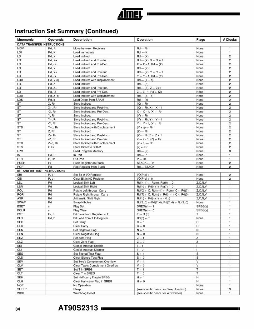
DATA TRANSFER INSTRUCTIONSMOV Rd, Rr Move between Registers Rd ← Rr None 1LDI Rd, K Load Immediate Rd ← K None 1LD Rd, X Load Indirect Rd ← (X) None 2LD Rd, X+ Load Indirect and Post-Inc. Rd ← (X), X ← X + 1 None 2LD Rd, -X Load Indirect and Pre-Dec. X ← X − 1, Rd ← (X) None 2LD Rd, Y Load Indirect Rd ← (Y) None 2LD Rd, Y+ Load Indirect and Post-Inc. Rd ← (Y), Y ← Y + 1 None 2LD Rd, -Y Load Indirect and Pre-Dec. Y ← Y − 1, Rd ← (Y) None 2LDD Rd, Y+q Load Indirect with Displacement Rd ← (Y + q) None 2LD Rd, Z Load Indirect Rd ← (Z) None 2LD Rd, Z+ Load Indirect and Post-Inc. Rd ← (Z), Z ← Z+1 None 2LD Rd, -Z Load Indirect and Pre-Dec. Z ← Z - 1, Rd ← (Z) None 2LDD Rd, Z+q Load Indirect with Displacement Rd ← (Z + q) None 2LDS Rd, k Load Direct from SRAM Rd ← (k) None 2ST X, Rr Store Indirect (X) ← Rr None 2ST X+, Rr Store Indirect and Post-Inc. (X) ← Rr, X ← X + 1 None 2ST -X, Rr Store Indirect and Pre-Dec. X ← X - 1, (X) ← Rr None 2ST Y, Rr Store Indirect (Y) ← Rr None 2ST Y+, Rr Store Indirect and Post-Inc. (Y) ← Rr, Y ← Y + 1 None 2ST -Y, Rr Store Indirect and Pre-Dec. Y ← Y - 1, (Y) ← Rr None 2STD Y+q, Rr Store Indirect with Displacement (Y + q) ← Rr None 2ST Z, Rr Store Indirect (Z) ← Rr None 2ST Z+, Rr Store Indirect and Post-Inc. (Z) ← Rr, Z ← Z + 1 None 2ST -Z, Rr Store Indirect and Pre-Dec. Z ← Z - 1, (Z) ← Rr None 2STD Z+q, Rr Store Indirect with Displacement (Z + q) ← Rr None 2STS k, Rr Store Direct to SRAM (k) ← Rr None 2LPM Load Program Memory R0 ← (Z) None 3IN Rd, P In Port Rd ← P None 1OUT P, Rr Out Port P ← Rr None 1PUSH Rr Push Register on Stack STACK ← Rr None 2POP Rd Pop Register from Stack Rd ← STACK None 2BIT AND BIT-TEST INSTRUCTIONSSBI P, b Set Bit in I/O Register I/O(P,b) ← 1 None 2CBI P, b Clear Bit in I/O Register I/O(P,b) ← 0 None 2LSL Rd Logical Shift Left Rd(n+1) ← Rd(n), Rd(0) ← 0 Z,C,N,V 1LSR Rd Logical Shift Right Rd(n) ← Rd(n+1), Rd(7) ← 0 Z,C,N,V 1ROL Rd Rotate Left through Carry Rd(0) ←=C, Rd(n+1) ← Rd(n), C ←=Rd(7) Z,C,N,V 1ROR Rd Rotate Right through Carry Rd(7) ←=C, Rd(n) ← Rd(n+1), C ←=Rd(0) Z,C,N,V 1ASR Rd Arithmetic Shift Right Rd(n) ← Rd(n+1), n = 0..6 Z,C,N,V 1SWAP Rd Swap Nibbles Rd(3..0) ←=Rd(7..4), Rd(7..4) ←=Rd(3..0) None 1BSET s Flag Set SREG(s) ← 1 SREG(s) 1BCLR s Flag Clear SREG(s) ← 0 SREG(s) 1BST Rr, b Bit Store from Register to T T ← Rr(b) T 1BLD Rd, b Bit Load from T to Register Rd(b) ← T None 1SEC Set Carry C ← 1 C 1CLC Clear Carry C ← 0 C 1SEN Set Negative Flag N ← 1 N 1CLN Clear Negative Flag N ← 0 N 1SEZ Set Zero Flag Z ← 1 Z 1CLZ Clear Zero Flag Z ← 0 Z 1SEI Global Interrupt Enable I ← 1 I 1CLI Global Interrupt Disable I ← 0 I 1SES Set Signed Test Flag S ← 1 S 1CLS Clear Signed Test Flag S ← 0 S 1SEV Set Two’s Complement Overflow V ← 1 V 1CLV Clear Two’s Complement Overflow V ← 0 V 1SET Set T in SREG T ← 1 T 1CLT Clear T in SREG T ← 0 T 1SEH Set Half-carry Flag in SREG H ← 1 H 1CLH Clear Half-carry Flag in SREG H ← 0 H 1NOP No Operation None 1SLEEP Sleep (see specific descr. for Sleep function) None 3WDR Watchdog Reset (see specific descr. for WDR/timer) None 1
Instruction Set Summary (Continued)Mnemonic Operands Description Operation Flags # Clocks
AT90S231384
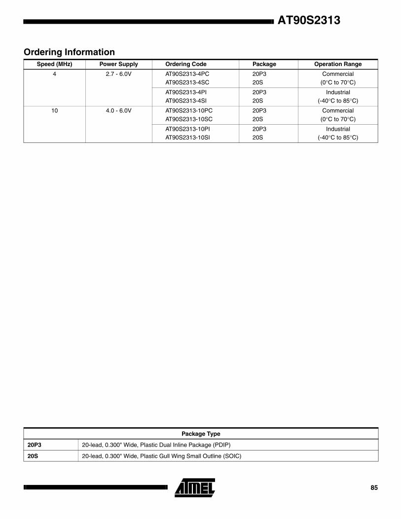
AT90S2313
Ordering InformationSpeed (MHz) Power Supply Ordering Code Package Operation Range
4 2.7 - 6.0V AT90S2313-4PCAT90S2313-4SC
20P320S
Commercial(0°C to 70°C)
AT90S2313-4PIAT90S2313-4SI
20P320S
Industrial(-40°C to 85°C)
10 4.0 - 6.0V AT90S2313-10PC
AT90S2313-10SC
20P3
20S
Commercial
(0°C to 70°C)
AT90S2313-10PIAT90S2313-10SI
20P320S
Industrial(-40°C to 85°C)
Package Type
20P3 20-lead, 0.300" Wide, Plastic Dual Inline Package (PDIP)
20S 20-lead, 0.300" Wide, Plastic Gull Wing Small Outline (SOIC)
85

Packaging Information
1.060(26.9).980(24.9) PIN
1
.280(7.11)
.240(6.10)
.090(2.29)MAX
.005(.127)MIN
.015(.381) MIN
.022(.559)
.014(.356).070(1.78).045(1.13)
.325(8.26)
.300(7.62)
015
REF
.430(10.92) MAX
.014(.356)
.008(.203)
.110(2.79)
.090(2.29)
.150(3.81)
.115(2.92)
SEATINGPLANE
.210(5.33)MAX
.900(22.86) REF
JEDEC STANDARD MS-001 BA
AT90S231386
0.299 (7.60)0.291 (7.39)
0.020 (0.508)0.013 (0.330)
0.420 (10.7)0.393 (9.98)
PIN 1
.050 (1.27) BSC
0.513 (13.0)0.497 (12.6)
0.012 (0.305)0.003 (0.076)
0.105 (2.67)0.092 (2.34)
08
REF
0.035 (0.889)0.015 (0.381)
0.013 (0.330)0.009 (0.229)
20P3, 20-lead, 0.300" Wide,Plastic Dual Inline Package (PDIP)Dimensions in Inches and (Millimeters)
20S, 20-lead, 0.300" Wide,Plastic Gull Wing Small Outline (SOIC)Dimensions in Inches and (Millimeters)
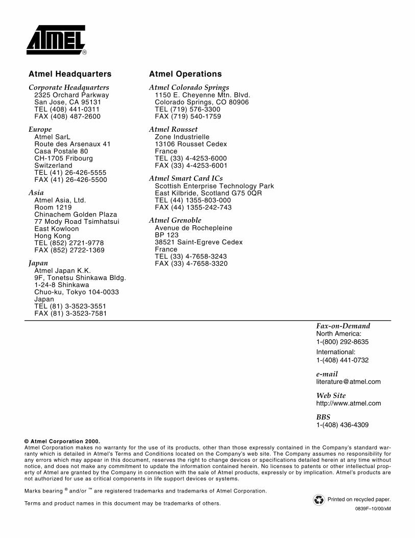
© Atmel Corporation 2000.Atmel Corporation makes no warranty for the use of its products, other than those expressly contained in the Company’s standard war-ranty which is detailed in Atmel’s Terms and Conditions located on the Company’s web site. The Company assumes no responsibility forany errors which may appear in this document, reserves the right to change devices or specifications detailed herein at any time withoutnotice, and does not make any commitment to update the information contained herein. No licenses to patents or other intellectual prop-erty of Atmel are granted by the Company in connection with the sale of Atmel products, expressly or by implication. Atmel’s products arenot authorized for use as critical components in life support devices or systems.
Atmel Headquarters Atmel Operations
Corporate Headquarters2325 Orchard ParkwaySan Jose, CA 95131TEL (408) 441-0311FAX (408) 487-2600
EuropeAtmel SarLRoute des Arsenaux 41Casa Postale 80CH-1705 FribourgSwitzerlandTEL (41) 26-426-5555FAX (41) 26-426-5500
AsiaAtmel Asia, Ltd.Room 1219Chinachem Golden Plaza77 Mody Road TsimhatsuiEast KowloonHong KongTEL (852) 2721-9778FAX (852) 2722-1369
JapanAtmel Japan K.K.9F, Tonetsu Shinkawa Bldg.1-24-8 ShinkawaChuo-ku, Tokyo 104-0033JapanTEL (81) 3-3523-3551FAX (81) 3-3523-7581
Atmel Colorado Springs1150 E. Cheyenne Mtn. Blvd.Colorado Springs, CO 80906TEL (719) 576-3300FAX (719) 540-1759
Atmel RoussetZone Industrielle13106 Rousset CedexFranceTEL (33) 4-4253-6000FAX (33) 4-4253-6001
Atmel Smart Card ICsScottish Enterprise Technology ParkEast Kilbride, Scotland G75 0QRTEL (44) 1355-803-000FAX (44) 1355-242-743
Atmel GrenobleAvenue de RochepleineBP 12338521 Saint-Egreve CedexFranceTEL (33) 4-7658-3243FAX (33) 4-7658-3320
Fax-on-DemandNorth America:1-(800) 292-8635
International:1-(408) 441-0732
Web Sitehttp://www.atmel.com
BBS1-(408) 436-4309
Printed on recycled paper.
0839F–10/00/xM
Marks bearing ® and/or ™ are registered trademarks and trademarks of Atmel Corporation.
Terms and product names in this document may be trademarks of others.