ARM architcture
57
Hossam Adel
-
Upload
hossam-adel -
Category
Engineering
-
view
611 -
download
5
Transcript of ARM architcture

Hossam Adel

Hossam Adel Mohammed
eg.linkedin.com/in/enghossam
Positions :
Electronics Engineer | Helwan Company for Engineering Industries (Military Factory 99).
Electronics Engineer |Ministry of Industry and Foreign Trade.
Embedded SW/HW Developer | IST Industries.
Embedded system Instructor at AMIT

Lecture Contents:
-Embedded Introduction.
1- ARM Overview.
2- ARM architecture
a- Pipeline
b- Memory management
- Cache, TCM, MMU, TLB and MPU
c- DMA “direct memory access controller ”
d-NEON ( SIMD ) unit and Multi-Tasks.
e- AMBA specifications.
f- Interworking with Tumb.
3- Security in ARM.
4- semihosting.

What’s mean of Embedded ?! Any system depend on MC / MP that called Embedded System.
An Embedded System is a computer system with a dedicated function.
Embedded systems are designed to do some specific task, rather than be a
general-purpose computer for multiple tasks.
SOC ?!
Ardunio & Raspberry PI.

How to Build suitable ES 1 - Select suitable MC.
2 - Select Peripherals.
3- Select OS (RTOS).
4 - Select Lang. Programmed.
a- Assembly
b- C/C++


ARM Ltd ARM founded in November 1990
Advanced RISC Machines
Company headquarters in Cambridge, UK Processor design centres in Cambridge, Austin, and Sophia Antipolis
Sales, support, and engineering offices all over the world
Best known for its range of RISC processor cores designs
Other products – fabric IP, software tools, models, cell libraries - to help partners develop and ship ARM-based SoCs
More information about ARM and our offices on our web site: http://www.arm.com/aboutarm/
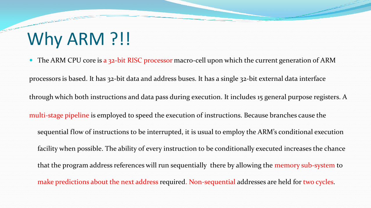
Why ARM ?!! The ARM CPU core is a 32-bit RISC processor macro-cell upon which the current generation of ARM
processors is based. It has 32-bit data and address buses. It has a single 32-bit external data interface
through which both instructions and data pass during execution. It includes 15 general purpose registers. A
multi-stage pipeline is employed to speed the execution of instructions. Because branches cause the
sequential flow of instructions to be interrupted, it is usual to employ the ARM’s conditional execution
facility when possible. The ability of every instruction to be conditionally executed increases the chance
that the program address references will run sequentially there by allowing the memory sub-system to
make predictions about the next address required. Non-sequential addresses are held for two cycles.
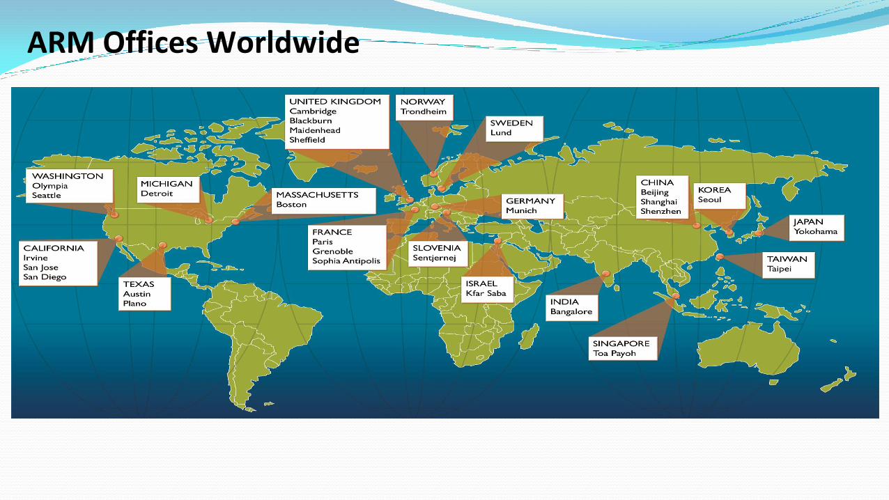
ARM Offices Worldwide

ARM Connected Community – 900+
Connect, Collaborate, Create – accelerating innovation

Embedded Processors

Application Processors
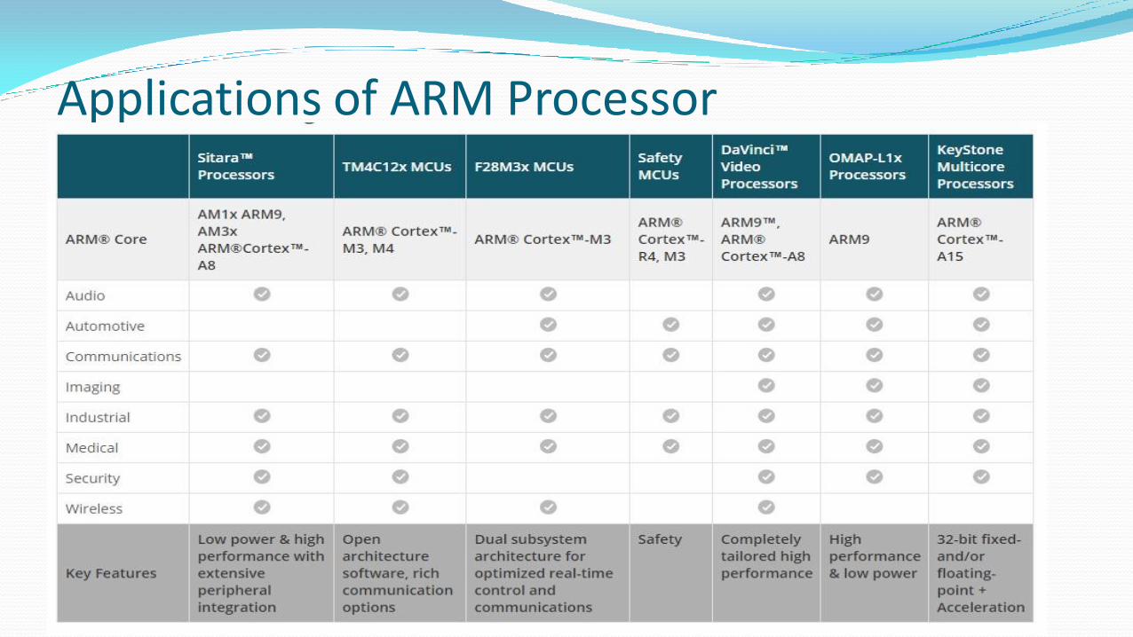
Applications of ARM Processor
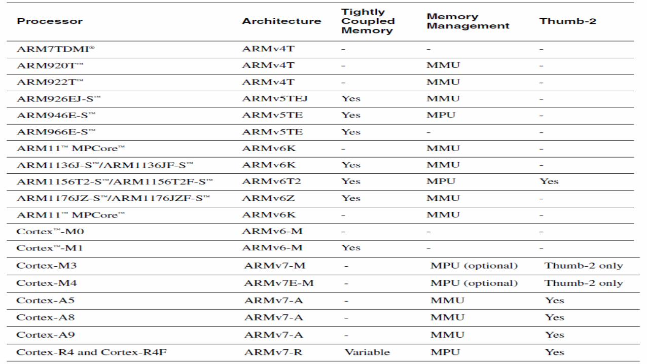

ARM Processor Family
Processor
family
# of pipeline
stages
Memory
organization
Clock
Rate
MIPS/MHz
ARM6 3 Von
Neumann
25 MHz
ARM7 3 Von
Neumann
66 MHz 0.9
ARM8 5 Von
Neumann
72 MHz 1.2
ARM9 5 Harvard 200 MHz 1.1
ARM10 6 Harvard 400 MHz 1.25
StrongARM 5 Harvard 233 MHz 1.15
ARM11 8 Von
Neumann/
Harvard
550 MHz 1.2
16

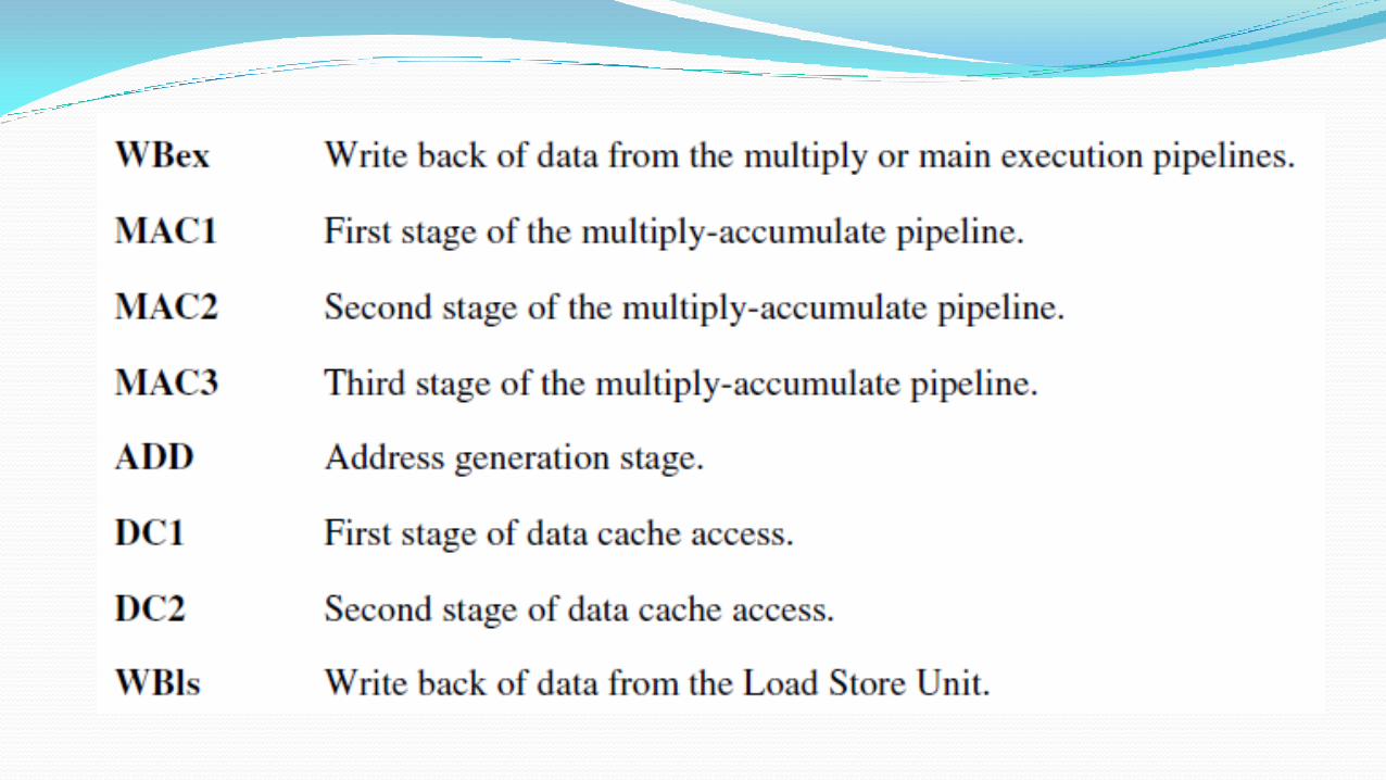
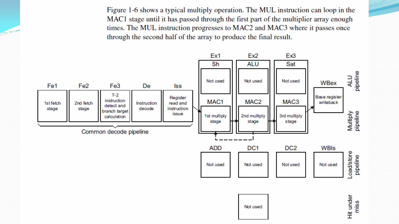
Pipeline :
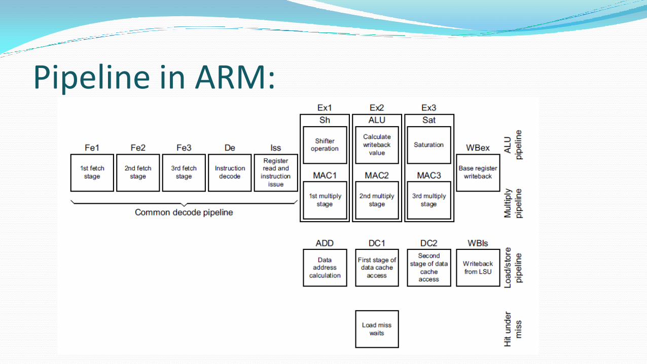
Pipeline in ARM:


System Control Coprocessorfunctions of the system control coprocessor are:
• overall system control and configuration
• optional cache configuration and management
• optional Tightly-Coupled Memory (TCM) configuration and management
• optional Memory Protection Unit (MPU) configuration and management
• debug accesses to the caches
• system performance monitoring.

Memory System of ARM1176JZ
Cache Organization
TCM - Tightly-coupled memory
MMU
TLB
MPU
DMA - Direct Memory Access

Memory Size and Speed
25
On-chip cache memory
registers
2nd-level off chip cache
Main memory
Hard disk
Access
timecapacity
Slow
Fast
Large
Small
Cost
Cheap
Expensive
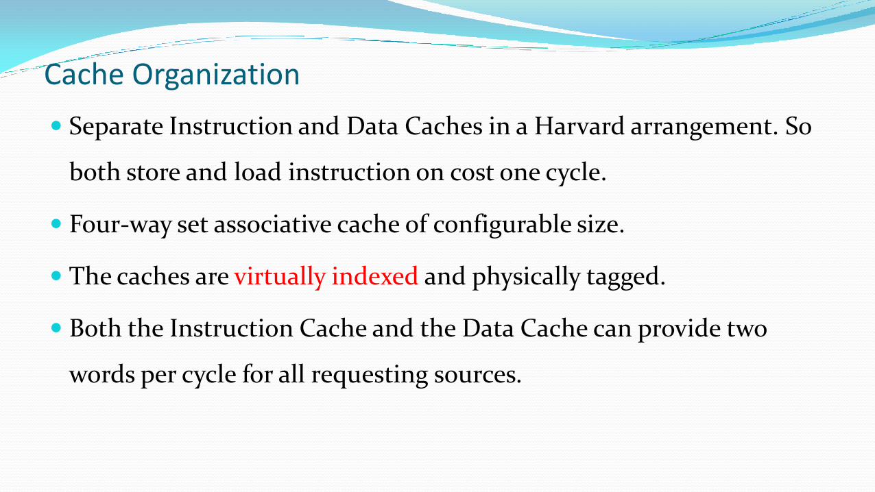
Cache Organization
Separate Instruction and Data Caches in a Harvard arrangement. So
both store and load instruction on cost one cycle.
Four-way set associative cache of configurable size.
The caches are virtually indexed and physically tagged.
Both the Instruction Cache and the Data Cache can provide two
words per cycle for all requesting sources.

Features of the cache system
The cache is a Harvard implementation (Separate Instruction and Data Caches ).
The other main operations performed by the cache is cache line Write-Back.
Cache replacement policies are Pseudo-Random or Round-Robin, Round-Robin
uses a single counter for all sets, that selects the way used for replacement.
Cache lines can be either Write-Back or Write-Through,
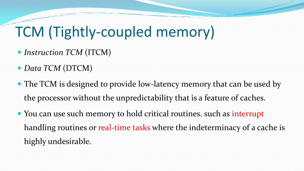
TCM (Tightly-coupled memory) Instruction TCM (ITCM)
Data TCM (DTCM)
The TCM is designed to provide low-latency memory that can be used by
the processor without the unpredictability that is a feature of caches.
You can use such memory to hold critical routines. such as interrupt
handling routines or real-time tasks where the indeterminacy of a cache is
highly undesirable.

TCM Behavior
TCM forms a continuous area of memory that is always valid if the TCM is enabled. The TCM is used
as part of the physical memory map of the system, and is not backed by a level of external memory
with the same physical addresses. For this reason, the TCM behaves differently from the caches for
regions of memory that are marked as being Write-Through Cachable. In such regions, no external
writes occur in the event of a write to memory locations contained in the TCM.
MMU Memory Management Unit
The processor MMU works with the cache memory system to control accesses to and
from external memory.
The MMU also controls the translation of virtual addresses to physical addresses.
The processor implements an ARMv6 MMU enhanced with features to provide address
translation and access permission checks for all ports of the processor.
While controlling the translation of virtual addresses to physical addresses, MMU in
ARM11 makes use of TLB (Translation Look aside Buffers)
TLB Translation Look aside Buffers
A single set of two-level page tables stored in main memory controls the
contents of the instruction and data side
Micro TLB
Main TLB

Micro TLB & Main TLB Micro TLB -- The first level of caching for the page table information is a small
Micro TLB of ten entries that is implemented on each of the instruction and
data sides.
You can configure Micro TLB replacement to be round-robin or random. By
default the round-robin replacement algorithm is used.
Main TLB -- the second layer in the TLB structure that catches the cache misses
from the Micro TLBs. It provides a centralized source for translation entries.
Misses from the instruction and data Micro TLBs are handled by a unified main

MPU Memory protection unit
The MPU supports 16 memory regions. Each region is programmed with a base address
and size, and can be overlayed to enable efficient programming of the memory map. To
support overlaying the regions are assigned priorities, with region 0 having the lowest
priority and region 15 having the highest. The MPU returns access permissions and
attributes for the highest priority region in which the address hits.

Enabling the MPU
When enabled, the behavior of the MPU is as follows:
• When the Load Store Unit or Pre-fetch Unit generates a memory access, the MPU
compares the memory address with the programmed memory regions.
• If the address does not exist in a memory region, a background fault is signalled
to the requesting block, along with status information to enable the Fault Status
Register to be correctly formed.
• If a matching memory region is found, then the region information is used:
1. The access permission bits are used to determine if the access is permitted.
If the access is not permitted the MPU signals a memory abort, otherwise
the access is permitted to proceed.
2. The memory region attributes are used to determine if the access is cached,
uncached or device and if it is shared.
• If the address matches in multiple memory regions, then a fixed priority scheme
selects the attributes for the highest numbered region.
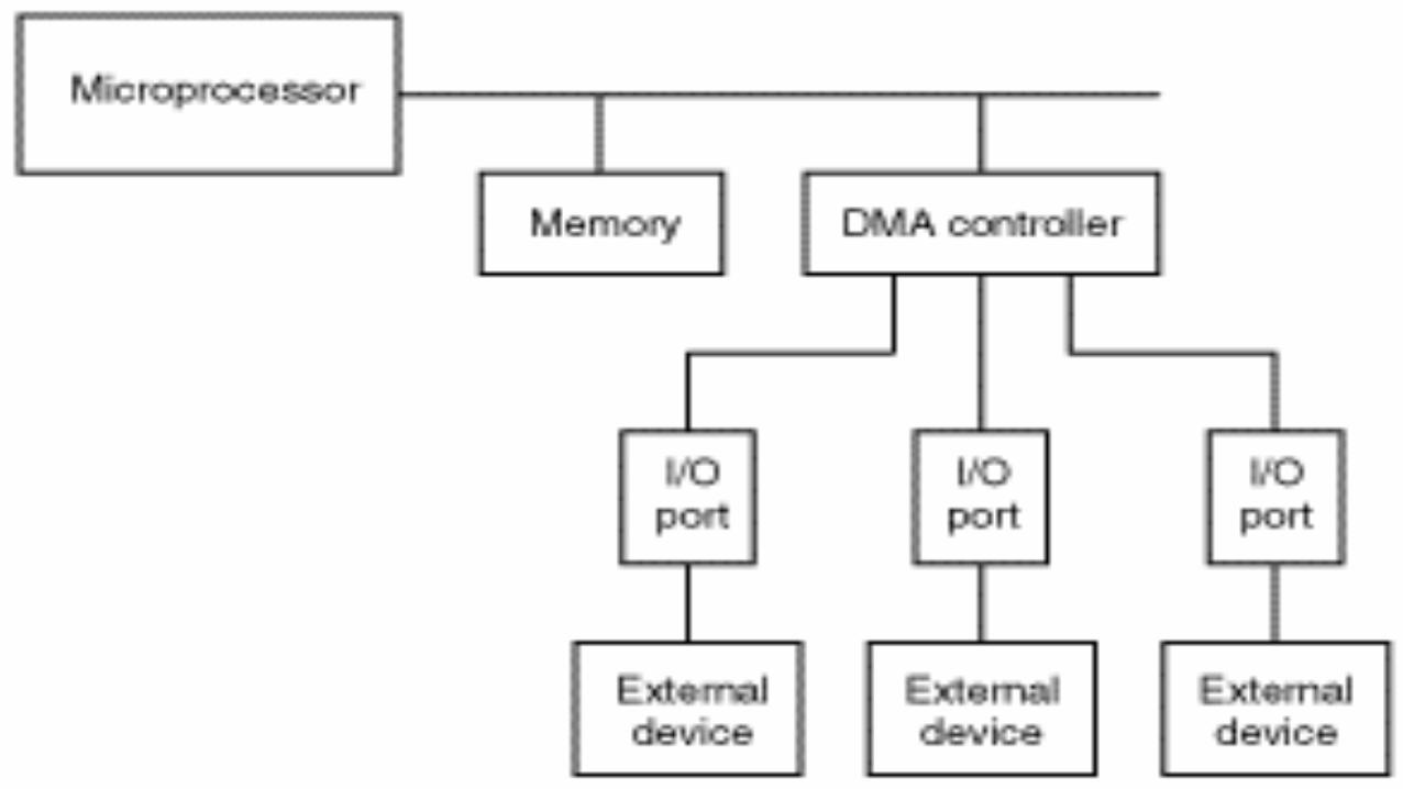
Direct memory access (DMA) Direct memory access (DMA) is a feature of computerized systems that allows certain
hardware subsystems to access main system memory independently of the central
processing unit (CPU).
Without DMA, when the CPU is using programmed input/output, it is typically fully
occupied for the entire duration of the read or write operation, and is thus unavailable
to perform other work. With DMA, the CPU initiates the transfer, does other operations
while the transfer is in progress, and receives an interrupt from the DMA controller
when the operation is done. This feature is useful any time the CPU cannot keep up
with the rate of data transfer, or where the CPU needs to perform useful work while
waiting for a relatively slow I/O data transfer.

Many hardware systems use DMA, including disk drive controllers, graphics
cards, network cards and sound cards. DMA is also used for intra-chip data
transfer in multi-core processors. Computers that have DMA channels can
transfer data to and from devices with much less CPU overhead than computers
without DMA channels. Similarly, a processing element inside a multi-core
processor can transfer data to and from its local memory without occupying its
processor time, allowing computation and data transfer to proceed in parallel.
DMA can also be used for "memory to memory" copying or moving of data
within memory. DMA can offload expensive memory operations, such as large
copies or scatter-gather operations, from the CPU to a dedicated DMA engine.
An implementation example is the I/O Acceleration Technology.

The NEON unit (SIMD) The NEON unit provides 32 vector registers that each hold 16 bytes of
information.
These 16 byte registers can then be operated on in parallel in the NEON unit.
For example, in one vector add instruction you can add eight 16-bit integers
to eight other16 bit integers to produce eight 16-bit results.
The NEON unit supports 8-bit, 16-bit and 32-bit integer operations, and
some 64-bit operations, in addition to 32-bit floating point operations.

What is NEON? NEON is a wide SIMD data processing architecture
Extension of the ARM instruction set (v7-A)
32 x 64-bit wide registers (can also be used as 16 x 128-bit wide registers)
NEON instructions perform “Packed SIMD” processing
Registers are considered as vectors of elements of the same data type
Data types available: signed/unsigned 8-bit, 16-bit, 32-bit, 64-bit, single prec. float
Instructions usually perform the same operation in all lanes
Dn
Dm
Dd
Lane
Source RegistersSource Registers
Operation
Destination Register
ElementsElementsElements
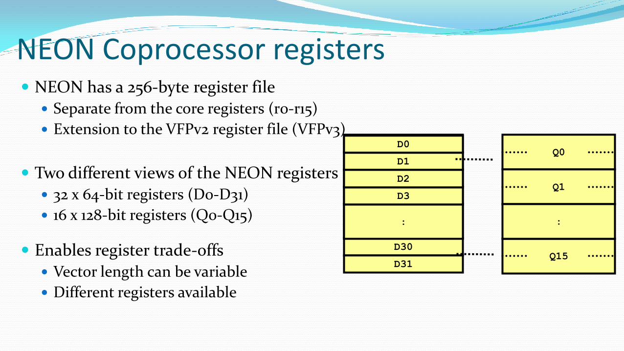
NEON Coprocessor registers NEON has a 256-byte register file Separate from the core registers (r0-r15)
Extension to the VFPv2 register file (VFPv3)
Two different views of the NEON registers
32 x 64-bit registers (D0-D31)
16 x 128-bit registers (Q0-Q15)
Enables register trade-offs
Vector length can be variable
Different registers available
Q0
Q1
Q15
:
D0
D1
D2
D3
:
D30
D31
D0
D1
D2
D3
:
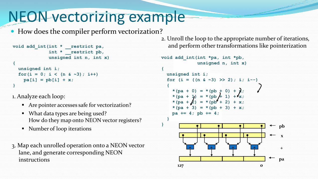
NEON vectorizing example How does the compiler perform vectorization?
void add_int(int * __restrict pa,
int * __restrict pb,
unsigned int n, int x)
{
unsigned int i;
for(i = 0; i < (n & ~3); i++)
pa[i] = pb[i] + x;
}
1. Analyze each loop:
Are pointer accesses safe for vectorization?
What data types are being used?How do they map onto NEON vector registers?
Number of loop iterations
void add_int(int *pa, int *pb,
unsigned n, int x)
{
unsigned int i;
for (i = ((n & ~3) >> 2); i; i--)
{
*(pa + 0) = *(pb + 0) + x;
*(pa + 1) = *(pb + 1) + x;
*(pa + 2) = *(pb + 2) + x;
*(pa + 3) = *(pb + 3) + x;
pa += 4; pb += 4;
}
}
2. Unroll the loop to the appropriate number of iterations, and perform other transformations like pointerization
+ + + +3. Map each unrolled operation onto a NEON vector lane, and generate corresponding NEON instructions
pb
x
pa
+
0127
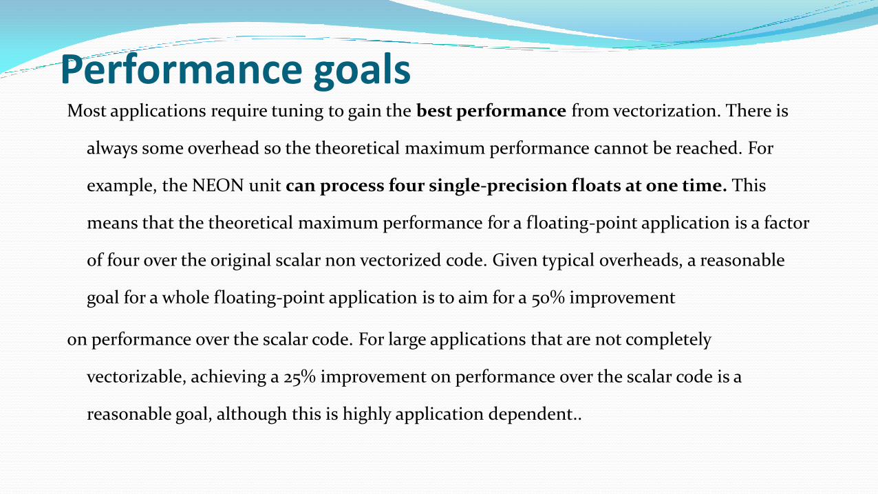
Performance goalsMost applications require tuning to gain the best performance from vectorization. There is
always some overhead so the theoretical maximum performance cannot be reached. For
example, the NEON unit can process four single-precision floats at one time. This
means that the theoretical maximum performance for a floating-point application is a factor
of four over the original scalar non vectorized code. Given typical overheads, a reasonable
goal for a whole floating-point application is to aim for a 50% improvement
on performance over the scalar code. For large applications that are not completely
vectorizable, achieving a 25% improvement on performance over the scalar code is a
reasonable goal, although this is highly application dependent..

AMBA specifications : The Advanced Microcontroller Bus Architecture.
Three distinct buses are defined within the AMBA specification:
the Advanced High-performance Bus (AHB)
the Advanced System Bus (ASB)
the Advanced Peripheral Bus (APB).


Advanced High-performance Bus (AHB) The AMBA AHB is for high-performance, high clock frequency system modules. The AHB acts as the high-performance system backbone bus. AHB supports the efficient connection of processors, on-chip memories and off-chip external memory interfaces with low-power peripheral macrocell functions. AHB is also specified to ensure ease of use in an efficient design flow using synthesis and automated test techniques.
Advanced System Bus (ASB) The AMBA ASB is for high-performance system modules. AMBA ASB is an alternative system bus suitable for use where the high-performance features of AHB are not required. ASB also supports the efficient connection of processors, on-chip memories and off-chip external memory interfaces with low-power peripheral macrocell functions.
Advanced Peripheral Bus (APB) The AMBA APB is for low-power peripherals. AMBA APB is optimized for minimal power consumption and reduced interface complexity to support peripheral functions. APB can be used in conjunction with either version of the system bus.
Objectives of the AMBA specification The AMBA specification has been derived to satisfy four key requirements:
• to facilitate the right-first-time development of embedded microcontroller
products with one or more CPUs or signal processors
• to be technology-independent and ensure that highly reusable peripheral and
system macro-Cells can be migrated across a diverse range of IC processes and be
appropriate for full-custom, standard cell and gate array technologies
• to encourage modular system design to improve processor independence,
providing a development road-map for advanced cached CPU cores and the
development of peripheral libraries
• to minimize the silicon infrastructure required to support efficient on-chip and
off-chip communication for both operation and manufacturing test.

Interworking with Tumb. What’s mean of Tumb.
Why Tumb code.
When you write code for an ARM processor that supports Thumb instructions, you
probably build most of your application to run in Thumb state. This gives the best code
density. With 8-bit or 16-bit wide memory, it also gives the best performance. However,
you might want parts of your application to run in ARM state for reasons such as:
Speed Some parts of an application might be speed critical. These sections
might be more efficient running in ARM state than in Thumb state.
Some systems include a small amount of fast 32-bit memory. ARM code
can be run from this without the overhead of fetching each instruction
from 8-bit or 16-bit memory.
Functionality
Thumb instructions are less flexible than their equivalent ARM
instructions. Some operations are not possible in Thumb state. A state
change to ARM is required to carry out the following operations:
• accesses to CPSR to enable or disable interrupts, and to change
mode,
• accesses to coprocessors
• execution of Digital Signal Processor (DSP) math instructions that
can not be performed in C language.

Exception handling
The processor automatically enters ARM state when a processor
exception occurs. This means that the first part of an exception handler
must be coded with ARM instructions, even if it reenters Thumb state to
carry out the main processing of the exception. At the end of such
processing, the processor must be returned to ARM state to return from
the handler to the main application.
Standalone Thumb programs
An ARM processor that supports Thumb instructions always starts in
ARM state. To run simple Thumb assembly language programs, add an
ARM header that carries out a state change to Thumb state and then calls
the main Thumb routine.

Security in ARM Global Platform based Trusted Execution
Environment and TrustZone® Ready
The foundations for trusted services
ARM® TrustZone® technology based Trusted
Execution Environment (TEE) as an important
component of delivering secure services (including
premium content) and applications. The paper then
describes how a correctly implemented TrustZone®
based TEE system can be “Secure by default”, and
robust against software attack.
The Four Compartment Security Model To protect against these security threats, ARM offers a four compartment security model that
provides increasing levels of security through a combination of reducing the attack surface and
increasing isolation. A system designer will typically use a combination of the following to
provide an appropriate level of protection of user and system assets:
Normal World - User mode/System mode - PL0/PL1 in ARMv7 or EL0/EL1 in ARMv8
Running processes or applications are isolated from each other by the operating system
and the MMU. Each executing process has it’s own addressable memory, isolated from
other processes, along with a set of capabilities and permissions are administered by the
operating system kernel which executes with System level privilege.
This is the normal operating state for application software together with the operating system
and is often referred to as the ‘Normal World’, in contrast to the ‘Trusted World’ described below.

Hypervisor Mode - PL2 in ARMv7 or EL2 in ARMv8 The hypervisor allows multiple instances of
the same or different operating systems to execute on the same processor as a virtual machine.
Each virtual machine can be isolated from each other, and through use of a System MMU, such as
the MMU-400, other bus masters can also be virtualized. This separation can be used to protect
and secure resources and assets in one virtual machine from other virtual machines.
Trusted World - Secure state or EL3 in ARMv8 Using the Trust Zone® security extensions,
allows the system to be physically partitioned into the secure and non-secure components. This
provides further isolation of assets and can be used to ensure that software operating within the
normal operating system cannot directly access secure memory or secure peripherals.
SecurCore processors enable physically separate, tamper proof ICs offering secured processing
and storage protected against both physical and software attack.
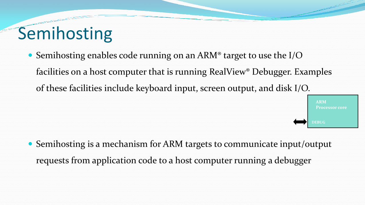
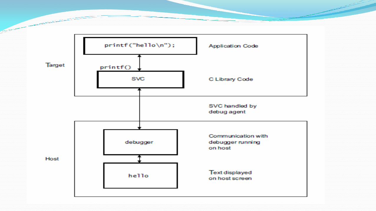
Semihosting Semihosting enables code running on an ARM® target to use the I/O
facilities on a host computer that is running RealView® Debugger. Examples
of these facilities include keyboard input, screen output, and disk I/O.
Semihosting is a mechanism for ARM targets to communicate input/output
requests from application code to a host computer running a debugger
ARMProcessor core
DEBUG

On chipmemory
Example ARM-based system ARM core deeply embedded within an SoC
External debug and trace via JTAG or CoreSightinterface
Design can have both external and internal memories
Varying width, speed and size – depending on system requirements
Can include ARM licensed CoreLink peripherals
Interrupt controller, since core only has two interrupt sources
Other peripherals and interfaces
Can include on-chip memory from ARM Artisan Physical IP Libraries
Elements connected using AMBA (Advanced Microcontroller Bus Architecture)
ARMProcessor core
AM
BA
AX
I
ExternalMemory Interface
APB Bridge
AM
BA
AP
B
CoreLink InterruptController
OtherCoreLink Peripherals
DMAPort
Clocks and Reset Controller
DEBUG
nIRQnFIQ
FLASH
SDRAM
ARM based SoCCustom Peripherals