IJESRT /Archives-2015/August... · http: // ... be considered in the power converter...
14
[Shah*, 4.(8): August, 2015] ISSN: 2277-9655 (I2OR), Publication Impact Factor: 3.785 http: // www.ijesrt.com © International Journal of Engineering Sciences & Research Technology [946] IJESRT INTERNATIONAL JOURNAL OF ENGINEERING SCIENCES & RESEARCH TECHNOLOGY MATLAB SIMULATIV STUDY OF SEPIC CONVERTER Ashfaq Shah*, S.P. Phulambrikar * Electrical Engg.Deptt. S.A.T.I. Vidisha, R.G.P.V. University, Bhopal(India). Electrical Engg.Deptt. S.A.T.I. Vidisha, R.G.P.V. University, Bhopal(India). ABSTRACT A high-power-factor rectifier suitable for universal line base on a modified version of the single-ended primary inductance converter (SEPIC) is presented in this. paper. The voltage multiplier.technique is applied to the classical SEPIC.circuit, obtaining new.operation characteristics as low-switch-voltage operation and high static gain at low.line voltage. The new configuration.also allows the reduction of the losses associated to the diode reverse.recovery current and soft commutation is obtained with a simple regenerative.snubber circuit. single-ended.primary inductance.converter (SEPIC) step up the input voltage 220 Vdc to 1200 Vdc with the switching frequency of 24 kHz. For close loop operation of single-ended primary inductance converter (SEPIC) with PI controller that uses to control the behaviors of the system in linear .This arrangement has close loop system. The computer program used for simulation of SEPIC is MATLAB SIMULINK & . This project consists of design, simulating the model and stability and other analysis of proposed model. KEYWORDS: single-ended primary inductanceconverter (SEPIC), high power factor (HPF), current controller (VCi) INTRODUCTION RESEARCH BACKGROUND Circuits run best with a steady and*specific input*Controlling the input to#specific#sub circuits is crucial for full filling design*requirements.*AC to AC *conversion*can*be easily*done with*the *transformer*however*dc dc*conversion*is*not*as*simple. Diodes#and#voltage*bridges*are useful for the reducing voltage by*a set*amount*but*can be inefficient. Voltage regulators are used to provide reference#voltage. %additionally battery voltage*decreases*as batteries discharge which can cause many*problems if there is no*voltage*control.*the most*efficient method of#regulating#voltage through a circuit is with the dc dc converter. There are*five*main#types#of#dc dc*converters. #Buck converters can only reduce voltage and boost converters only increase*voltage and buck boost CUK and SEPIC converters can increase or decrease the voltage. NEED FOR A BETTER TECHNIQUE Can deliver high boost *ratio with*minimum voltage and current stress being imposed on the Switches so that*moderately rated# (for example 30 V to 100 V range) MOSFETs rectifiers may be used. Can*operate*at moderate*duty*cycles (for example less than 85% to 90%)*for easier CCM *and PWM*control. Are true switchers without *the drawbacks# (including low output current) overcharge pumps Avoid*the*voltage3spikes and*ringing*associated with transformer*leakage*inductance. Some applications of*converters only*need to buck or*boost the voltage*and can simply*use the*corresponding converters. However#sometimes#the desired output voltage #will be in the range*of input*voltage*when*this is the*case*it is*usually best to use a*converter that can decrease or increase the voltage Buck boost converters*can be cheaper because they only*require a single*inductor% and *capacitor.*However*these*converters*suffer*from a high*amountinput *current*ripple*this#ripple*can*create*harmonic*in*many*applications these*harmonics*#using a large8capacitor or *an LC filter.*This often makes the buck and boost expensive or inefficient.*Another*issue*that can*complicate*the*usage*of buck boost *converters*is* that they*invert the*voltage.*CUK*converters*solve*both of*these problems by using extra*capacitor*and*inductor.*However*both*CUK*and*buck boost#converter#operation#cause#large#amounts*of#electrical#stress*on*the#components#this
-
Upload
trinhthien -
Category
Documents
-
view
216 -
download
3
Transcript of IJESRT /Archives-2015/August... · http: // ... be considered in the power converter...
[Shah*, 4.(8): August, 2015] ISSN: 2277-9655
(I2OR), Publication Impact Factor: 3.785
http: // www.ijesrt.com © International Journal of Engineering Sciences & Research Technology
[946]
IJESRT INTERNATIONAL JOURNAL OF ENGINEERING SCIENCES & RESEARCH
TECHNOLOGY
MATLAB SIMULATIV STUDY OF SEPIC CONVERTER Ashfaq Shah*, S.P. Phulambrikar
* Electrical Engg.Deptt. S.A.T.I. Vidisha, R.G.P.V. University, Bhopal(India).
Electrical Engg.Deptt. S.A.T.I. Vidisha, R.G.P.V. University, Bhopal(India).
ABSTRACT A high-power-factor rectifier suitable for universal line base on a modified version of the single-ended primary
inductance converter (SEPIC) is presented in this. paper. The voltage multiplier.technique is applied to the classical
SEPIC.circuit, obtaining new.operation characteristics as low-switch-voltage operation and high static gain at low.line
voltage. The new configuration.also allows the reduction of the losses associated to the diode reverse.recovery current
and soft commutation is obtained with a simple regenerative.snubber circuit. single-ended.primary
inductance.converter (SEPIC) step up the input voltage 220 Vdc to 1200 Vdc with the switching frequency of 24 kHz.
For close loop operation of single-ended primary inductance converter (SEPIC) with PI controller that uses to control
the behaviors of the system in linear .This arrangement has close loop system. The computer program used for
simulation of SEPIC is MATLAB SIMULINK & . This project consists of design, simulating the model and stability
and other analysis of proposed model.
KEYWORDS: single-ended primary inductanceconverter (SEPIC), high power factor (HPF), current controller (VCi)
INTRODUCTION
RESEARCH BACKGROUND Circuits run best with a steady and*specific input*Controlling the input to#specific#sub circuits is crucial for full
filling design*requirements.*AC to AC *conversion*can*be easily*done with*the *transformer*however*dc
dc*conversion*is*not*as*simple. Diodes#and#voltage*bridges*are useful for the reducing voltage by*a
set*amount*but*can be inefficient. Voltage regulators are used to provide reference#voltage. %additionally battery
voltage*decreases*as batteries discharge which can cause many*problems if there is no*voltage*control.*the
most*efficient method of#regulating#voltage through a circuit is with the dc dc converter. There
are*five*main#types#of#dc dc*converters. #Buck converters can only reduce voltage and boost converters only
increase*voltage and buck boost CUK and SEPIC converters can increase or decrease the voltage.
NEED FOR A BETTER TECHNIQUE Can deliver high boost*ratio with*minimum voltage and current stress being imposed on the Switches so
that*moderately rated# (for example 30 V to 100 V range) MOSFETs rectifiers may be used.
Can*operate*at moderate*duty*cycles (for example less than 85% to 90%)*for easier CCM *and
PWM*control.
Are true switchers without*the drawbacks# (including low output current) overcharge pumps
Avoid*the*voltage3spikes and*ringing*associated with transformer*leakage*inductance.
Some applications of*converters only*need to buck or*boost the voltage*and can simply*use the*corresponding
converters. However#sometimes#the desired output voltage #will be in the range*of input*voltage*when*this is
the*case*it is*usually best to use a*converter that can decrease or increase the voltage Buck boost converters*can be
cheaper because they only*require a single*inductor% and *capacitor.*However*these*converters*suffer*from a
high*amountinput*current*ripple*this#ripple*can*create*harmonic*in*many*applications these*harmonics*#using
a large8capacitor or *an LC filter.*This often makes the buck and boost expensive or inefficient.*Another*issue*that
can*complicate*the*usage*of buck boost*converters*is* that they*invert the*voltage.*CUK*converters*solve*both
of*these problems by using extra*capacitor*and*inductor.*However*both*CUK*and*buck
boost#converter#operation#cause#large#amounts*of#electrical#stress*on*the#components#this

[Shah*, 4.(8): August, 2015] ISSN: 2277-9655
(I2OR), Publication Impact Factor: 3.785
http: // www.ijesrt.com © International Journal of Engineering Sciences & Research Technology
[947]
can*resulting*device*failure*or overheating.# *THE*BOOST*converter*is#the&usual&structure#utilized#in* high
power factor*(HPF)#rectifiers in order to improve power factor*(PF)*and reduce the total*current
harmonic*distortion (THD). However for universal input*voltage*application*the efficiency can be*reduced*mainly
in the lowest input voltage and the worst*operation*condition must be considered in the power converter
design#procedure. #the improvement of the*efficiency at lower line voltage is important because the thermal design
and heat*sinks size are*defined considering#the#worst#operation point. Many works were#develope in order
#improve the operation*characteristics of the power*converter utilize in HPF#universal#input#rectifers. A review
of*the main*single-phase topologies*and techniques used in an*HPF rectifier*is presented in*discussion*about*the
use of single stage and two stages structures is*presented in two switches topology for universal input HPF#rectifier
is presented in.*some single stage isolated%HPF%rectifiers are%presented in. The use of% high static gain and% low
switch*voltage topologies can*improve the*efficiency operating with*low input voltage,*as presented in. The voltage
multiplier*technique was presented in for a*boost*converter in order to increase the static gain with reduced switch
voltage. However*the boost voltage doublers cannot be used for a universal input voltage HPF rectifier because
the*output voltage must be*higher than the double of the*maximum input*voltage modification*in the multiphase
boost#voltage#doubler was#proposed in for a#universal input HPF rectifier#in order to#obtain high static#gain at the
lower#input voltage with the#same dc#output voltage#level of a classical boost converter (Vo = 400 V).
The integration of a voltage*multiplier cell*with a classical*single ended primary*inductance converter*(SEPIC)*is
proposed in this paper in*order to obtain a*high step-up*static gain operating with low input voltage and a low step-
up static gain for the high input voltage operation. The operation#characteristics#obtained with this modification
makes the proposed*structure an interesting alternative for the*universal input HPF*rectifier or wide input*voltage
range applications#operating#with high*efficiency.*The*proposed converter*operates*with a*switch voltage lower
than the output voltage and with an input current*ripple lower than the*classical boost converter. The power circuit
of the proposed converter can be integrated with a simple regenerative#snubber obtaining soft switching commutation
and increasing the efficiency.
Main goal in power electronics is to transform electrical energy from on form to another to make electrical energy to
reach the load with highest efficiency is the target to be achieved power electronics*also target to*reduce the*size of
the device to*convert*these energy*which aims to reduce cost,*smaller in size and*high availability in*this project
the*power electronics device that use to dc to dc converter.
The dc-dc converter*for this*project*is single*ended primary*inductance converter.*it is use to convert unregulated*
dc input to a*controlled dc*output with*desired*voltage*level. The*single*indeed*primary*inductance converter
step up the input voltage*220 Vdc to 1200 Vdc*with the switching frequency 24 kHz. For#close loop operation#of
SEPIC with PI#controller that uses to control the behaviors of the system in linear .This arrangement is #close loop
system The software is#use to do*simulation is*MATLAB SIMULINK*this project*consists
of*designing*simulation and*stability and*other*analysis.
INTRODUCTION
A dc*converter can be*considered as dc*equivalent to an ac*transformer with a*continuously variable turn ratio like
a*transformer it is used to step*down or step up a dc voltage*source. There are various dc dc*converters such as buck
(step down) boost (step up) and*buck-boost and cuk*converter the basic*step down and step up*converters can
be*transformed into a number of new topologies by bringing in the tapped inductor. Switching regulators are preferred
over linear regulators for their high efficiency and providing step up step down or inverter*output unlike
linear*regulator*which does only step-down operations in reality the conversion*efficiency of linear*regulators
is*limited to only 30% and they find*application in analog*circuits to*ensure nearly constant*Supply voltage
providing high*power supply*rejection ratio .In*switching controller circuits*semiconductor*switches regulate the
dynamic transfer of power from input to output with very short transition times due to this switching action there is
ripple added to output voltage the output should be a dc#voltage with a minimum superimposition of ac ripple. Pulse
width modulations is the most*widely used method for*controlling the output*voltage. It holds a constant*switching
*frequency and*varies the duty cycle. Duty cycle is*well defined*as the*ratio of switch*on time to reciprocal of
the*switching frequency*Meanwhile the switching*frequency is fixed this modulation#arrangement#has a relatively
narrow noise spectrum allowing a simple low pass*filter to sharply#reduce#peak to peak ripple at output voltage his
requirement is achieved*by arranging an inductor*and capacitor in the converter in such a manner as to form a low
pass filter network this*needs the*frequency of low pass*filter to be much*less than switching frequency*The

[Shah*, 4.(8): August, 2015] ISSN: 2277-9655
(I2OR), Publication Impact Factor: 3.785
http: // www.ijesrt.com © International Journal of Engineering Sciences & Research Technology
[948]
following section discusses*various converter*topologies*and their operation Perfect*circuits are consider for
ease*of understanding and*explanation the main difference between each is the arrangement of the*switches and
output filter*inductor and capacitor.
GENERAL
The purpose of this project is to design and optimize a SEPIC dc to dc#converter The#SEPIC converter allows a
range of dc#voltage to readjusted to maintain the constant voltage output. This project talks about the importance of
dc to dc#converters and why SEPIC converters are used instead of other dc to dc#converters. This project also #detail
about how to#control the output of the converter with either potentiometer or feedback to show how it can be
implements a circuit from these projections learns dc to dc converter optimization and control.
PROPOSED SEPIC Converter TOPOLOGY
The proposed SEPIC Converter is illustrated in Fig 3.1
Fig 2.1 Modified SEPIC converter
The power circuit*of classical SEPIC*converter is*presented in the*stepup and stepdown static*gains of the
SEPIC*converter is an*interesting operation*characteristic for a*wide input*thvoltage range*application however
the*switch voltage is*equal to the*sum of the input and*output voltages*this topology*is not used*for
universal*input HPF*rectifier.
The voltage*multiplier technique was*presented in order to*increase the static*gain of*single-phase*and
multiphase*boost dc to dc*converters. An*adaptation of the*voltage multiplier*technique*with the SEPIC*the
inclusion of the*diode Dm and the*capacitor Cm. Many operational characteristic*Cs of the classical SEPIC
converter*are changed with proposed*modification
CONTROL SCHEME Control algorithm of the*proposed converter*is based on classical*structure of the average*current mode
control*with the digital*implementation and the*power system*operating in CCM. The*design procedure of
the*control system for the*boost converter is*well established and*used in this*implementation. The
implementation*of the control*system for the*proposed converter*is accomplished*by using*exactly the
same*control designed for the*classical boost converter this*approximations is possible*because the*additional
poles*inserted by the*inductor L2 and*capacitors Cs and Cm*occur in a*frequency higher*than the poles*inserter by
*inductor L1 and the*output

[Shah*, 4.(8): August, 2015] ISSN: 2277-9655
(I2OR), Publication Impact Factor: 3.785
http: // www.ijesrt.com © International Journal of Engineering Sciences & Research Technology
[949]
Filter*capacitor Co the capacitors Cs and Cm are very*small comparing*with the output*filter capacitor.
The*inductor L2 is also a*made of the input*inductor L1. As the*crossing frequencies*of voltage and current*control
loops are*lower than *frequency of the*lower frequency*poles the*additional higher*frequency poles does
not*present a significant*influence in the phase*margin and the*gain margin thus*maintaining approximately*the
same*dynamic response*for both*power stage*structures in order*to show this characteristic the same*control
algorithm*designed for the*classical boost*converter is*used with the*proposed converter*and the
experimental*results*obtained confirm this*consideration. The control*algorithm is*developed*using the
MC56F8013 digital*signal controller*operating with a*sampling rate equal to 24 kHz. The*sample of the*output
voltage is*compared with a*reference of the*output voltage The*error signal obtained *is applied to a*digital
proportional integral*controller. The result obtained*from the voltage*controller is*multiplied by a*sample of
the*rectified input voltage and the*resultant signal*is the reference*waveform for the*current control*loop (iref ).
The sampling of the*rectified input*current is compared*with the current*reference. The result (Ei) is*applied to
a*digital PI controller. The output*of the current*controller (VCi) is*applied to the pulse*width modulator*generating
the command*signal of the power*switch.
OPERATING PRINCIPLE OF SEPIC CONVERTER
The*capacitor CM is charged*with the output*voltage of the*classical boost*converter. Therefore*the voltage
applied*to the inductor L2 during the*conduction of the*power switch is higher than*that in the*classical SEPIC
thereby*increasing the*static gain. The*polarity of the voltage*stored in the*capacitor CS is inverted*in the
proposed*converter the*continuous conduction*mode operation of the*modified SEPIC converter*presents
the*following two*operation*stages.
[1] First stage ([t0 to t1]:-At the instant t0 the switch S is turned-offhand the energy stored in the input inductor
L1 is transferred to the output through the capacitor CS and output diode Do and also to the capacitor Cm
through the diode Dm Therefore the switch voltage is equal to the capacitor Cm voltage. The energy stored
in the inductor L2 is transferred to the output through the diode Do.
Fig.2.2 first operation stage

[Shah*, 4.(8): August, 2015] ISSN: 2277-9655
(I2OR), Publication Impact Factor: 3.785
http: // www.ijesrt.com © International Journal of Engineering Sciences & Research Technology
[950]
[2] Second stage ([t1, At the instant t1 the switch S is turned on and the diodes Dm and Do are blocked and the
inductors L1 and L2 store#energyThe input voltage is applied to the input inductor L1 and the voltage VCs
Vcm is applied to the inductor L2 . The voltage Vcm is higher than the voltage VCs.
Fig.2.3 second operation stage
The main theoretical waveforms operating with hard switching commutation are presented in Fig. 2.4

[Shah*, 4.(8): August, 2015] ISSN: 2277-9655
(I2OR), Publication Impact Factor: 3.785
http: // www.ijesrt.com © International Journal of Engineering Sciences & Research Technology
[951]
Fig.2.4 main theoretical waveforms operating with hard switching commutation
The voltage in all diodes and the power switch is equal to the capacitor CM voltage. The output voltage is equal to the
sum of the Cs and Cm capacitors voltages. The average L1 inductor current is equal to the input current and the
average L2 inductor current is equal to the output current.
PWM AND TRANSISTORS PWM is the main part in designing a buck converter. By using pulse-width modulation (PWM) control controlling of
output voltage is achieved by varying the duty cycle of the switch. Duty cycle intends to ratio of the period where
power semiconductor is kept ON to the cycle period. Pulse width modulation (PWM) is a powerful technique for
controlling analog circuits with a processor's digital outputs.PWM is operating in a wide variety of applications starts
from measurement and communications to power control and conversion Control of PWM is usually effected by an
IC is necessary for controlling the output. The transistor switch is the most important thing of the switched supply and
controls the power delivered to the load. And also Power MOSFET’s are more suitable than BJT at power output of
[Shah*, 4.(8): August, 2015] ISSN: 2277-9655
(I2OR), Publication Impact Factor: 3.785
http: // www.ijesrt.com © International Journal of Engineering Sciences & Research Technology
[952]
the order of 50 W. when selecting a transistor also must consider its fast switching times and able to withstand the
voltage spikes produced by the inductor
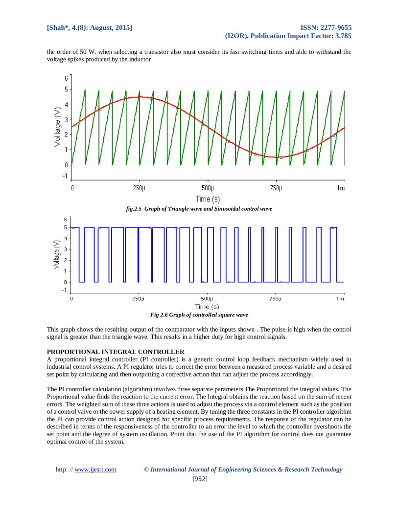
fig.2.5 Graph of Triangle wave and Sinusoidal control wave
Fig 2.6 Graph of controlled square wave
This graph shows the resulting output of the comparator with the inputs shown . The pulse is high when the control
signal is greater than the triangle wave. This results in a higher duty for high control signals.
PROPORTIONAL INTEGRAL CONTROLLER
A proportional integral controller (PI controller) is a generic control loop feedback mechanism widely used in
industrial control systems. A PI regulator tries to correct the error between a measured process variable and a desired
set point by calculating and then outputting a corrective action that can adjust the process accordingly.
The PI controller calculation (algorithm) involves three separate parameters The Proportional the Integral values. The
Proportional value finds the reaction to the current error. The Integral obtains the reaction based on the sum of recent
errors. The weighted sum of these three actions is used to adjust the process via a control element such as the position
of a control valve or the power supply of a heating element. By tuning the three constants in the PI controller algorithm
the PI can provide control action designed for specific process requirements. The response of the regulator can be
described in terms of the responsiveness of the controller to an error the level to which the controller overshoots the
set point and the degree of system oscillation. Point that the use of the PI algorithm for control does not guarantee
optimal control of the system.
[Shah*, 4.(8): August, 2015] ISSN: 2277-9655
(I2OR), Publication Impact Factor: 3.785
http: // www.ijesrt.com © International Journal of Engineering Sciences & Research Technology
[953]
Proportional term The proportional term makes a change to the output that is proportional to the current error value. The proportional
response may be adjusted by multiplying the error by a constant Kp termed the proportional gain.
The proportional term is given by:
Pout = Kpe(t)
· Io: Integral output
· Ki: Integral Gain
· e: Error = SP – PV
· τ: Time in the past involvement to the integral responses
A high proportional gain results in a large change in the output for a given change in the error. When proportional
gain is too high the system can become unstable In contrast a little gain results in a small output response to a large
input error and a less responsive controller. When proportional gain is too low the regulate action may be too small
when responding to system disturbances.
In the absence of disturbances pure proportional control will not settle at its target value but will maintain a steady
state error that is a function of the proportional gain and the process gain. Despite the steady state offset both tuning
principle and industrial practice indicate that it is the proportional term that should contribute the bulk of the output
change.
Integral term
The contribution from the integral term is proportional to both the magnitude of the error and the duration of the error.
Adding the instantaneous error over time gives the accumulated offset that should have been corrected previously.
The emerged error is then multiplied by the integral gain and added to the controller output. The magnitude of the
involvement of the integral term to the overall control action is determined by the integral gain Ki.
The integral term is given by:
Ki ∫ 𝑒 𝑡
0 d
Where
· Io: Integral output
· Ki: Integral Gain, a tuning parameter
· e: Error = SP – PV
· τ: Time in the past involvement to the integral responses
The integral term (when added to the proportional term) accelerates the movement of the process towards set point
and eliminates the residual steady-state error that occurs with a proportional only controller. Meanwhile the integral
term is responding to accumulated errors from the past it can introduce the present value to overshoot the set point
value cross over the set point and then create a deviation in the other direction.
DESIGN AND SIMULATION OF CIRCUITS Duty Cycle Calculation:
The amount that the SEPIC converters step up or down the voltage depends primarily on the Duty Cycle and the
parasitic elements in the circuit. The output of an ideal SEPIC converter is
𝑉𝑜 =D∗Vi
1−D
However this does not account for losses due to parasitic elements such as the diode drop VD. These make the equation
𝑉𝑜 + 𝑉𝑑 =D ∗ Vi
1 − D
This becomes
𝐷 =Vo + Vd
Vi + Vo + Vd

[Shah*, 4.(8): August, 2015] ISSN: 2277-9655
(I2OR), Publication Impact Factor: 3.785
http: // www.ijesrt.com © International Journal of Engineering Sciences & Research Technology
[954]
The maximum Duty Cycle will occur when the input voltage is at the minimum. If VD=.5V the
𝐷𝑚𝑖𝑛 =1200V+0.5V
120V+1200V+0.5V ≈ .91
The minimum duty cycle will occur when the input voltage is at the maximum.
𝐷𝑚𝑖𝑛 =1200V+0.5V
220V+1200V+0.5V ≈ 8.4
Inductor Calculation
In theory*the larger the*inductors are the*better the circuit will*operate and reduce*the ripple. However,
larger*inductors are more*expensive and*have a larger internal*resistance. This*greater internal*resistance will
make*the converter less*efficient. Creating*the best converter requires*choosing inductors*that are just
large*enough to keep*the voltage*and current ripple at an*acceptable*amount.
𝐿 =Vi min(Dmax)
∆io max Fsw =
120∗.63
(0.5A)∗50Khz = 3 mH inductors with low internal*resistance and*around 3mH will be ideal*for both
of the*inductors in the circuit.
GENERAL
Simulation has*become a very powerful*tool on the industry*application as well*as in ac ademi Cs nowadays.
This*is now essential*for an electrical*engineer to understand*the concept of simulation and learn*its use in
various*applications. matlab Simulator*is one of the best*ways to study the system*or circuit behavior*without
damging*it The tools*for performng*the simulation on*computer in*various fields*are available*in the market
for*engineering professional*Lots of industries*are spending a considerable*amount of time and*money in
doing*simulation before*manufacturing*their product. In majority*of the research*and development (R&D)
work*the simulation*plays a very*important role. Without*simulation of proposed models*it is quiet impossible*to
proceed*further. It must be noted*that in power electroniCs, matlab*simulation and a proof
of*concept*hardware*prototype in the*laboratore are complimentary to*each other. While
computer*simulation*must not be considered as*substitute for hardware*prototype. The goal of*this chapter is to
describe*simulation of impedance*source inverter*with R R L and RLE loads*using MATLAB tool.
SIMULATION RESULT
Simulations are carried for proposed SEPIC converter in both open and closed loops.
PROPOSED METHOD – SEPIC converter circuit
The Simulation circuit of the proposed SEPIC converter

[Shah*, 4.(8): August, 2015] ISSN: 2277-9655
(I2OR), Publication Impact Factor: 3.785
http: // www.ijesrt.com © International Journal of Engineering Sciences & Research Technology
[955]
Fig 3.1 Simulation circuit of SEPIC converter
The output voltage is shown in the Fig.3.2
[Shah*, 4.(8): August, 2015] ISSN: 2277-9655
(I2OR), Publication Impact Factor: 3.785
http: // www.ijesrt.com © International Journal of Engineering Sciences & Research Technology
[956]
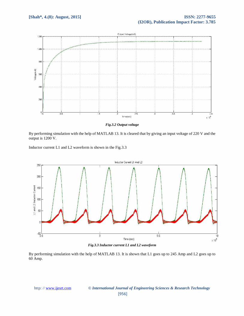
Fig.3.2 Output voltage
By performing simulation with the help of MATLAB 13. It is cleared that by giving an input voltage of 220 V and the
output is 1200 V.
Inductor current L1 and L2 waveform is shown in the Fig.3.3
Fig.3.3 Inductor current L1 and L2 waveform
By performing simulation with the help of MATLAB 13. It is shown that L1 goes up to 245 Amp and L2 goes up to
60 Amp.
[Shah*, 4.(8): August, 2015] ISSN: 2277-9655
(I2OR), Publication Impact Factor: 3.785
http: // www.ijesrt.com © International Journal of Engineering Sciences & Research Technology
[957]
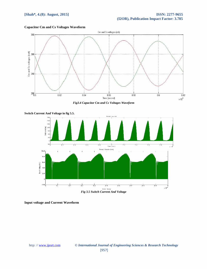
Capacitor Cm and Cs Voltages Waveform
Fig3.4 Capacitor Cm and Cs Voltages Waveform
Switch Current And Voltage in fig 5.5.
Fig 3.5 Switch Current And Voltage
Input voltage and Current Waveform

[Shah*, 4.(8): August, 2015] ISSN: 2277-9655
(I2OR), Publication Impact Factor: 3.785
http: // www.ijesrt.com © International Journal of Engineering Sciences & Research Technology
[958]
Fig 3.6 Input voltage and Current Waveform
5.4 Comparison of Theoretical Output waveform and Simulated Output Waveform
Fig. 3.7
CONCLUSION A modified*version of the*SEPIC*converter is*proposed for the*implementation of a*high-PF rectifier*suitable
for*universal line*application. Although*the proposed*structure*presents a*higher*circuit complexity*than
the*classical boost*converter*the advantages*obtained are*the higher#static gain for the#operation with the#lower
input#voltage range#lower#switch voltage#operation higher efficiency#operation#with the lowest#input
voltage#lower input#current#ripple and easy#integration with a#regenerative#snubber. Three snubber#circuits

[Shah*, 4.(8): August, 2015] ISSN: 2277-9655
(I2OR), Publication Impact Factor: 3.785
http: // www.ijesrt.com © International Journal of Engineering Sciences & Research Technology
[959]
are*proposed in*order to obtain a*reduction of the diode*reverse recovery*current problem, and also*obtaining turn-
on and*turn-off soft*switching for all input*voltage ranges*and*output power*variation. The average*current
mode*control is used*for the classical*boost converter*and also for*the proposed*converter, and the*dynamic
response*obtained with*both converters is*approximately the*same. The experimental*results are*obtained with*the
implementation*of a rectifier*with an output*Voltage equal to Vo = 1200 Volt for an*input voltage*of 220V.
REFERENCES [1] H. Cheng, K. Smedley, and A. Abramovitz, “Wide input wide output (WIWO)dc–dc converter,” IEEE
Transactions on Power Electronics, vol. 25, no. 2, Feb 2010.
[2] D. Maksimovic and S. Cuk, “Switching converter with wide dc conversion range,” IEEE Trans. Power Electron.,
vol. 6, no. 1, pp. 151–157, Jan. 1991.
[3] K. Yao, M. Ye, M. Xu, and F. C. Lee, “Tapped-inductor buck converter for high-step-down dc–dc conversion,”
IEEE Trans. Power Electron., vol. 20, no. 4, pp. 775–780, Jul. 2005.
[4] J.-H. Park and B.-H. Cho, “Nonisolation soft-switching buck converter with tapped-inductor for wide-input
extreme step-down applications,” IEEE Trans. Circuits Syst. I, Reg. Papers, vol. 54, no. 8, pp. 1809–1818,Aug. 2007.
[5] K. Yao, Y. Ren, J. Wei, M. Xu, and F. Lee, “A family of buck type dc–dc converters with autotransformers,” in
Proc. Appl. Power Electron. Conf. Expo. (APEC 2003), pp. 114–120.
[6] K. Nishijima, K. Abe, D. Ishida, T. Nakano, T. Nabeshima, T. Sato, and K. Harada, “A novel tapped-inductor
buck converter for divided power distribution system,” in Proc. IEEE PESC Conf. (PESC 2006), Jun., 18–22, pp. 1–
6.
[7] G. Spiazzi and S. Buso, “Power factor preregulator based on modified tapped-inductor buck converter,” in Proc.
IEEE PESC Conf., 1998, vol. 2, pp. 873–879.
[8] F. L. Luo and H. Ye, “Positive output cascade boost converters,” Proc. Inst. Electr. Eng. Electr. Power Appl., vol.
151, no. 5, pp. 590–606, Sep.2004.
[9] Q. Zhao and F. C. Lee, “High efficiency, high step-up dc–dc converters,” IEEE Trans. Power Electron., vol. 18,
no. 1, pp. 65–73, Jan. 2003.
[10] N. Vazquez, L. Estrada, C. Hernandez, and E. Rodriguez, “The tapped- inductor boost converter,” in Proc. IEEE
Int. Symp. Ind. Electron., Jun.,4–7, 2007, pp. 538–543.