LT8710 - Synchronous SEPIC/ Inverting/Boost … · and can be easily configured for boost, SEPIC,...
44
LT8710 1 8710f For more information www.linear.com/LT8710 TYPICAL APPLICATION FEATURES DESCRIPTION Synchronous SEPIC/ Inverting/Boost Controller with Output Current Control The LT ® 8710 is a synchronous PWM DC/DC controller with a rail-to-rail output current monitor and control. The LT8710 is ideal for many types of power supply topologies and can be easily configured for boost, SEPIC, inverting, or flyback configurations. The LT8710’s rail-to-rail output current monitor and control allows the part to be configured in current limited applica- tions such as battery charging. The FLAG pin can be used as a power good indication or C/10 indication allowing for accurate bulk and float battery voltages. The LT8710’s switching frequency range can be set be- tween 100kHz and 750kHz using an external resistor or synchronized to an external clock. The LT8710 also features innovative EN/FBIN pin cir- cuitry that allows for slowly varying input signals and an adjustable undervoltage lockout function. The pin is also used for input voltage regulation to avoid collapsing a high impedance input supply. Additional features such as frequency foldback and soft-start are integrated. The LT8710 is available in a 20-lead TSSOP package. 300kHz Inverter Generates –5V from a 4.5V to 25V Input APPLICATIONS L, LT, LTC, LTM, Linear Technology and the Linear logo are registered trademarks of Linear Technology Corporation. All other trademarks are the property of their respective owners. Protected by U.S. Patents, Including 7579816. n Wide Input Range: 4.5V to 80V n Rail-to-Rail Output Current Monitor and Control n Input Voltage Regulation for High Impedance Inputs n C/10 or Power Good Indication Pin n MODE Pin for Forced CCM or Pulse-Skipping Operation n Switching Frequency Up to 750kHz n Easily Configurable as a Boost, SEPIC, Inverting or Flyback Converter with Single Feedback Pin n Can Be Synchronized to External Clock n High Gain EN/FBIN Pin Accepts Slowly Varying Input Signals n 20-Lead TSSOP Package n High Power Local Power Supply n Wide Input Voltage Range SEPIC/Inverting n Lead Acid Battery Charger n Automotive Engine Control Unit (ECU) Power n Solar Panel Power Converter Efficiency and Power Loss IMON SS GND CSP TG CSN BG LT8710 8710 TA01a MODE INTV CC RT SYNC V IN EN/FBIN BIAS INTV EE FBX FLAG V C ISN ISP V OUT –5V 7A V IN 4.5V TO 25V 13.3k 2.2μH 120μF 2.2μF 100μF ×2 10k 10μF ×4 118k 1.5m 4m 2.2μH • • 10μF ×2 60.4k 11.5k 2.2μF INTV CC 330μF + 47nF 220nF 3.3nF 100pF + 499Ω 0.47μF LOAD CURRENT (A) 0 EFFICIENCY (%) POWER LOSS (W) 100 80 90 70 65 50 40 30 20 8 6 7 5 4 3 2 1 0 1 4 5 6 8710 TA01b 7 2 3 V IN = 5V V IN = 12V
Transcript of LT8710 - Synchronous SEPIC/ Inverting/Boost … · and can be easily configured for boost, SEPIC,...

LT8710
18710f
For more information www.linear.com/LT8710
Typical applicaTion
FeaTures DescripTion
Synchronous SEPIC/ Inverting/Boost Controller with
Output Current Control
The LT®8710 is a synchronous PWM DC/DC controller with a rail-to-rail output current monitor and control. The LT8710 is ideal for many types of power supply topologies and can be easily configured for boost, SEPIC, inverting, or flyback configurations.
The LT8710’s rail-to-rail output current monitor and control allows the part to be configured in current limited applica-tions such as battery charging. The FLAG pin can be used as a power good indication or C/10 indication allowing for accurate bulk and float battery voltages.
The LT8710’s switching frequency range can be set be-tween 100kHz and 750kHz using an external resistor or synchronized to an external clock.
The LT8710 also features innovative EN/FBIN pin cir-cuitry that allows for slowly varying input signals and an adjustable undervoltage lockout function. The pin is also used for input voltage regulation to avoid collapsing a high impedance input supply. Additional features such as frequency foldback and soft-start are integrated. The LT8710 is available in a 20-lead TSSOP package.
300kHz Inverter Generates –5V from a 4.5V to 25V Input
applicaTions
L, LT, LTC, LTM, Linear Technology and the Linear logo are registered trademarks of Linear Technology Corporation. All other trademarks are the property of their respective owners. Protected by U.S. Patents, Including 7579816.
n Wide Input Range: 4.5V to 80Vn Rail-to-Rail Output Current Monitor and Controln Input Voltage Regulation for High Impedance Inputsn C/10 or Power Good Indication Pinn MODE Pin for Forced CCM or Pulse-Skipping
Operationn Switching Frequency Up to 750kHzn Easily Configurable as a Boost, SEPIC, Inverting or
Flyback Converter with Single Feedback Pinn Can Be Synchronized to External Clockn High Gain EN/FBIN Pin Accepts Slowly Varying Input
Signalsn 20-Lead TSSOP Package
n High Power Local Power Supplyn Wide Input Voltage Range SEPIC/Invertingn Lead Acid Battery Chargern Automotive Engine Control Unit (ECU) Powern Solar Panel Power Converter
Efficiency and Power Loss
IMON SSGND
CSP TGCSNBG
LT8710
8710 TA01a
MODE
INTVCC
RT
SYNC
VIN
EN/FBINBIAS
INTVEE
FBX
FLAGVC
ISN
ISP
VOUT –5V7A
VIN4.5V TO 25V
13.3k
2.2µH
120µF
2.2µF
100µF×2
10k
10µF×4
118k
1.5m
4m
2.2µH• •10µF ×2
60.4k
11.5k
2.2µFINTVCC
330µF+
47nF 220nF 3.3nF
100pF
+
499Ω
0.47µF
LOAD CURRENT (A)0
EFFI
CIEN
CY (%
)
POWER LOSS (W
)
100
80
90
70
65
50
40
30
20
8
6
7
5
4
3
2
1
01 4 5 6
8710 TA01b
72 3
VIN = 5VVIN = 12V
LT8710
28710f
For more information www.linear.com/LT8710
pin conFiguraTion
absoluTe MaxiMuM raTings(Note 1)
FE PACKAGE20-LEAD PLASTIC TSSOP
1
2
3
4
5
6
7
8
9
10
TOP VIEW
20
19
18
17
16
15
14
13
12
11
FBX
VC
SS
FLAG
IMON
ISN
ISP
BIAS
INTVEE
TG
GND
SYNC
RT
MODE
EN/FBIN
CSP
CSN
VIN
INTVCC
BG
21GND
TJMAX = 125°C, θJA = 38°C/W, θJC = 10°C/W
EXPOSED PAD (PIN 21) IS GND, MUST BE SOLDERED TO PCB
orDer inForMaTionLEAD FREE FINISH TAPE AND REEL PART MARKING* PACKAGE DESCRIPTION TEMPERATURE RANGE
LT8710EFE#PBF LT8710EFE#TRPBF LT8710FE 20-Lead Plastic TSSOP –40°C to 125°C
LT8710IFE#PBF LT8710IFE#TRPBF LT8710FE 20-Lead Plastic TSSOP –40°C to 125°C
Consult LTC Marketing for parts specified with wider operating temperature ranges. *The temperature grade is identified by a label on the shipping container.For more information on lead free part marking, go to: http://www.linear.com/leadfree/ For more information on tape and reel specifications, go to: http://www.linear.com/tapeandreel/
VIN Voltage ................................................ –0.3V to 80VBIAS Voltage .............................................. –0.3V to 80VEN/FBIN Voltage ......................................... –0.3V to 80VBG Voltage ............................................................Note 5TG Voltage ............................................................Note 5RT Voltage ................................................... –0.3V to 5V SS Voltage ................................................... –0.3V to 3VFBX Voltage .................................................................5VFBX Current ............................................................–1mAVC Voltage .................................................... –0.3V to 2VSYNC Voltage ............................................ –0.3V to 5.5VFLAG Voltage ............................................... –0.3V to 7VFLAG Current ......................................................... ±1mA
MODE Voltage ............................................ –0.3V to 40VINTVCC Voltage ............................................ –0.3V to 7VINTVEE Voltage......................................................Note 5CSP Voltage ................................................. –0.3V to 2VCSN Voltage ................................................. –0.3V to 2VISP Voltage ................................. ISN – 0.4V to ISN + 2VISN Voltage ................................................ –0.3V to 80VIMON Voltage ............................................ –0.3V to 2.5VOperating Junction Temperature Range LT8710E ............................................. –40°C to 125°C LT8710I .............................................. –40°C to 125°CStorage Temperature Range .................. –65°C to 150°CLead Temperature (Soldering, 10 sec) ................... 300°C

LT8710
38710f
For more information www.linear.com/LT8710
elecTrical characTerisTics
PARAMETER CONDITIONS MIN TYP MAX UNITS
Minimum Operating Input Voltage VIN OR VBIAS VIN if VBIAS ≥ 4.5V
l 0
4.25 4.5 V V
Quiescent Current, IVIN VBIAS = VISN = 7.5V, Not Switching VBIAS = 6.3V, VINTVEE = VISN = 0V, Not Switching
4 5.5
5.5 7.5
mA mA
Quiescent Current in Shutdown VEN/FBIN = 0V 0 1 µA
EN/FBIN Active Mode EN/FBIN Rising l 1.64 1.7 1.76 V
EN/FBIN Chip Enable EN/FBIN Rising EN/FBIN Falling
l
l
1.22 1.18
1.3 1.26
1.38 1.34
V V
EN/FBIN Chip Enable Hysteresis 44 mV
EN/FBIN Input Voltage Low Shutdown Mode l 0.3 V
EN/FBIN Pin Bias Current VEN/FBIN = 3V VEN/FBIN = 1.7V VEN/FBIN = 1.6V VEN/FBIN = 0V
14 13
44 19.5 17.5
0
60 25
22.5 0.1
µA µA µA µA
SS Charge Current VSS = 0V, Current Flows Out of SS Pin l 7 10.1 13.8 µA
SS Low Detection Voltage Part Exiting Undervoltage Lockout l 18 50 82 mV
SS Hi Detection Voltage SS Rising SS Falling
1.5 1.3
1.8 1.7
2.1 2.05
V V
SS Hi Detection Hysteresis 100 mV
Low Dropout Regulators, INTVCC and INTVEE
INTVCC Voltage IINTVCC = 10mA l 6.2 6.3 6.4 V
INTVCC Undervoltage Lockout INTVCC Rising INTVCC Falling
l
l
3.88 3.5
4 3.73
4.12 3.95
V V
INTVCC Undervoltage Lockout Hysteresis 270 mV
INTVCC Dropout Voltage VIN – INTVCC, VIN = 6V, VBIAS = 0V, IINTVCC = 10mA VBIAS – VINTVCC, VIN = 0V, VBIAS = 6V, IINTVCC = 10mA
255 280
mV mV
INTVCC Load Regulation VIN = 12V, VBIAS = 0V, IINTVCC = 0mA to 80mA VIN = 0V, VBIAS = 12V, IINTVCC = 0mA to 40mA
–0.44 –0.34
–2 –2
% %
INTVCC Line Regulation 10V ≤ VIN ≤ 80V, VBIAS = 0V, IINTVCC = 10mA 10V ≤ VBIAS ≤ 80V, VIN = 0V, IINTVCC = 10mA
–0.003 –0.006
–0.03 –0.03
%/V %/V
INTVCC Maximum External Load Current 5 mA
INTVEE Voltage, VBIAS – VINTVEE IINTVEE = 10mA l 6.03 6.18 6.33 V
INTVEE Undervoltage Lockout, VBIAS – VINTVEE
VBIAS – VINTVEE Rising VBIAS – VINTVEE Falling
l
l
3.24 2.94
3.42 3.22
3.6 3.48
V V
INTVEE Undervoltage Lockout Hysteresis, VBIAS – VINTVEE
200 mV
INTVEE Dropout Voltage, VINTVEE VBIAS = 6V, IINTVEE = 10mA 0.75 V
Control Loops (Refer to Block Diagram to Locate Amplifiers)
Current Limit Voltage, VCSP – VCSN VFBX = 1.1V, Minimum Duty Cycle VFBX = 1.1V, Maximum Duty Cycle
l
l
46 23
50 31
54 38
mV mV
VFBX = 1.4V, MODE = 0V, Minimum Duty Cycle VFBX = 1.4V, MODE = 0V, Maximum Duty Cycle
l
l
–23 –38
–32 –51
–41 –65
mV mV
FBX Positive Output Regulation Voltage, EA1
l 1.191 1.213 1.237 V
FBX Negative Output Regulation Voltage, EA2
l –2 9.6 21 mV
The l denotes the specifications which apply over the full operating temperature range, otherwise specifications for each channel are at TA = 25°C. VIN = 12V, VEN/FBIN = 12V, VBIAS = 12V, unless otherwise noted (Note 2).

LT8710
48710f
For more information www.linear.com/LT8710
PARAMETER CONDITIONS MIN TYP MAX UNITS
Positive FBX Pin Bias Current VFBX = Positive FBX Reg Voltage, Current into Pin l 81.9 83.7 85.6 µA
Negative FBX Pin Bias Current VFBX = Negative FBX Reg Voltage, Current Out of Pin l 81.1 83.1 85.2 µA
FBX Amp Transconductance, EA1 or EA2
ΔI = 2μA 200 µmhos
FBX Amp Voltage Gain, EA1 or EA2 70 V/V
FBX Line Regulation 4.5V ≤ VIN ≤ 80V, VBIAS = 0V –0.02 –0.001 0.02 %/V
Output Current Sense Regulation Voltage, VISP – VISN
VISN = 80V, VFBX = 1V VISN = 12V, VFBX = 1V VISN = 0V, VFBX = 1V VISN = 12V, VFBX = 1V, INTVEE in UVLO and VSS > 1.8V
l
l
l
l
43 43 40 17
50 50 50 25
57 57 60 34
mV mV mV mV
IMON Regulation Voltage, EA3 VFBX = 1V VFBX = 1V, INTVEE in UVLO and VSS > 1.8V
l
l
1.184 0.885
1.213 0.916
1.24 0.947
V V
Output Current Sense Amp Transconductance, A6
ΔI = 10μA 1000 µmhos
Output Current Sense Amp Voltage Gain, A6
11.9 V/V
Output Current Sense Amp Input Dynamic Range, A6
Negative Input Range, VISP – VISN Positive Input Range, VISP – VISN
500
–51.8 mV mV
IMON Amp Transconductance, EA3 ΔI = 2μA, VFBX = 1V 165 µmhos
IMON Amp Voltage Gain, EA3 VFBX = 1V 65 V/V
EN/FBIN Input Regulation Voltage, EA4 VFBX = 1V l 1.55 1.607 1.662 V
EN/FBIN Amp Transconductance, EA4 ΔI = 2µA, VFBX = 1V 140 µmhos
EN/FBIN Amp Voltage Gain, EA4 VFBX = 1V 55 V/V
MODE Forced CCM Threshold To Exit Forced CCM Mode, MODE Rising To Enter Forced CCM Mode, MODE Falling
l
l
1.19 1.125
1.224 1.175
1.258 1.23
V V
MODE Forced CCM Threshold Hysteresis
49 mV
DCM Comparator Threshold in Pulse-Skipping Mode, MODE = 2V
VISN = 80V, To Enter DCM Mode, VISP – VISN Falling VISN = 12V, To Enter DCM Mode, VISP – VISN Falling VISN = 0V, To Enter DCM Mode, VISP – VISN Falling
l
l
l
–4.5 –4.5 –7.5
2.8 2.8 2.8
10 10 13
mV mV mV
DCM Comparator Threshold in Forced CCM, MODE =0V
VISN = 80V, To Enter DCM Mode, VISP – VISN Falling VISN = 12V, To Enter DCM Mode, VISP – VISN Falling VISN = 0V, To Enter DCM Mode, VISP – VISN Falling
l
l
l
–220 –220 –220
–300 –300 –300
–380 –380 –380
mV mV mV
Oscillator
Switching Frequency, fOSC RT = 46.4k RT = 357k
l
l
640 85
750 100
860 115
kHz kHz
Switching Frequency in Foldback Compared to Normal fOSC 1/5 ratio
Switching Frequency Range Free-Running or Synchronizing l 100 750 kHz
SYNC High Level for Sync l 1.5 V
SYNC Low Level for Sync l 0.4 V
SYNC Clock Pulse Duty Cycle VSYNC = 0V to 3V 20 80 %
Recommended Min SYNC Ratio fSYNC/fOSC
3/4
elecTrical characTerisTics The l denotes the specifications which apply over the full operating temperature range, otherwise specifications for each channel are at TA = 25°C. VIN = 12V, VEN/FBIN = 12V, VBIAS = 12V, unless otherwise noted (Note 2).

LT8710
58710f
For more information www.linear.com/LT8710
PARAMETER CONDITIONS MIN TYP MAX UNITS
Gate Drivers, BG and TG
BG Rise Time CBG = 3300pF (Note 3) 24 ns
BG Fall Time CBG = 3300pF (Note 3) 21 ns
TG Rise Time CTG = 3300pF (Note 3) 15 ns
TG Fall Time CTG = 3300pF (Note 3) 16 ns
BG and TG Non-Overlap Time TG Rising to BG Rising, CBG = CTG = 3300pF (Note 3) BG Falling to TG Falling, CBG = CTG = 3300pF (Note 3)
80 45
140 90
220 150
ns ns
BG Minimum On-Time CBG = CTG = 3300pF 150 420 ns
BG Minimum Off-Time CBG = CTG = 3300pF 100 480 ns
TG Minimum On-Time CBG = CTG = 3300pF 0 150 ns
TG Minimum Off-Time CBG = CTG = 3300pF 290 770 ns
C/10 and Power Good Indicators, FLAG
FLAG C/10 Indicator Threshold VISP – VISN Falling, VFBX = 1.215V VISP – VISN Rising, VFBX = 1.215V
l
l
1 4
5 10
16 23
mV mV
FLAG C/10 Indicator Hysteresis 5 mV
FLAG Power Good Threshold for Positive FBX Voltage
VFBX Rising, VISP – VISN = 0V VFBX Falling, VISP – VISN = 0V
l
l
1.127 1.062
1.153 1.095
1.184 1.126
V V
FLAG Power Good Threshold for Negative FBX Voltage
VFBX Falling, VISP – VISN = 0V VFBX Rising, VISP – VISN = 0V
l
l
46 103
68.5 126
90 152
mV mV
FLAG Power Good Hysteresis for Positive or Negative FBX Voltage
58 mV
FLAG Anti-Glitch Delay from C/10 or Power Good Threshold Trip to FLAG Toggle
100
µs
FLAG Output Voltage Low 100µA into FLAG Pin l 9 50 mV
FLAG Leakage Current VFLAG = 7V, FLAG Off 0.01 1 µA
Note 1: Stresses beyond those listed under Absolute Maximum Ratings may cause permanent damage to the device. Exposure to any Absolute Maximum Rating condition for extended periods may affect device reliability and lifetime.Note 2: The LT8710E is guaranteed to meet performance specifications from 0°C to 125°C junction temperature. Specifications over the –40°C to 125°C operating temperature range are assured by design, characterization and correlation with statistical process controls. The LT8710I is guaranteed over the full –40°C to 125°C operating junction temperature range.
Note 3: Rise and fall times are measured using 10% and 90% levels. Delay times are measured using 50% levels.Note 4: This IC includes overtemperature protection that is intended to protect the device during momentary overload conditions. Junction temperature will exceed 125°C when overtemperature protection is active. Continuous operation over the specified maximum operating junction temperature may impair device reliability.Note 5: Do not apply a positive or negative voltage or current source to the BG, TG, and INTVEE pins, otherwise permanent damage may occur.
elecTrical characTerisTics The l denotes the specifications which apply over the full operating temperature range, otherwise specifications for each channel are at TA = 25°C. VIN = 12V, VEN/FBIN = 12V, VBIAS = 12V, unless otherwise noted (Note 2).

LT8710
68710f
For more information www.linear.com/LT8710
Positive and Negative Output Voltage Regulation (FBX)
Positive and Negative FBX Current at Output Voltage Regulation
Input Voltage Regulation (EN/FBIN)
Input Voltage Regulation vs FBX (EN/FBIN)
Output Current Sense Regulation Voltage (ISP-ISN and IMON)
Output Current Sense Regulation Voltage vs FBX (ISP-ISN and IMON)
Max Current Limit vs Duty Cycle (CSP - CSN)
Max Current Limit vs Temperature at Min DC (CSP - CSN)
Max Current Limit vs SS (CSP - CSN)
Typical perForMance characTerisTics TA = 25°C, unless otherwise noted.
DUTY CYCLE (%)0
MAX
POS
ITIV
E CS
P-CS
N (m
V)
MAX NEGATIVE CSP-CSN (m
V)
60
50
55
40
30
45
35
25
20
–20
–30
–25
–40
–50
–35
–45
–55
–605020 70 80 90
8710 G01
10030 4010 60
fOSC = 300kHz
TEMPERATURE (°C)–50
MAX
POS
ITIV
E CS
P-CS
N (m
V)M
AX NEGATIVE CSP-CSN (mV)
56
52
54
50
48
46
44
–26
–30
–28
–34
–32
–36
–3850–25 75 100
8710 G02
1250 25SS (V)
0.0
CSP-
CSN
(mV)
60
40
50
30
20
10
00.80.2 1 1.2 1.4
8710 G03
1.60.4 0.6
TEMPERATURE (°C)–50
EN/F
BIN
VOLT
AGE
(V)
1.63
1.61
1.62
1.60
1.59
1.58
1.57–25 50 75 100
8710 G06
1250 25
FBX (V)0.6
EN/F
BIN
(V)
2.0
1.8
1.9
1.7
1.6
1.5
1.40.7 1 1.1 1.2
8710 G07
1.30.8 0.9
TEMPERATURE (°C)–50
POSI
TIVE
FBX
VOL
TAGE
(V)
NEGATIVE FBX VOLTAGE (mV)
1.2225
1.2175
1.2200
1.2150
1.2125
1.2100
1.2075
15.0
10.0
12.5
7.5
5.0
2.5
0–25 50 75 100
8710 G04
1250 25TEMPERATURE (°C)
–50
POSI
TIVE
FBX
CUR
RENT
INTO
PIN
(µA)
NEGATIVE FBX CURRENT OUT OF PIN (µA)
86
84
85
83
82
81
80
86
84
85
83
82
81
80–25 50 75 100
8710 G05
1250 25
TEMPERATURE (°C)–50
AVER
AGE
ISP-
ISN
(mV)
IMON (V)
57.5
52.5
55.0
50.0
47.5
45.0
42.5
1.2175
1.2125
1.2150
1.2100
1.2075
1.2050
1.2025–25 50 75 100
8710 G08
1250 25
IMON
AVE ISP-ISN
FBX (V)0.6
AVER
AGE
ISP-
ISN
(mV)
IMON (V)
60
50
55
45
40
35
30
1.30
1.20
1.25
1.15
1.10
1.05
1.000.7 1 1.1 1.2
8710 G09
1.30.8 0.9
IMON
AVE ISP-ISN

LT8710
78710f
For more information www.linear.com/LT8710
MODE Forced CCM ThresholdsEN/FBIN Chip Enable and Active Mode Thresholds EN/FBIN Pin Current
Oscillator Frequency vs Temperature
Oscillator Frequency During Soft-Start BG and TG Transition Time
DCM Thresholds (ISP-ISN) Power Good Thresholds (FBX) C/10 Thresholds (ISP-ISN)
Typical perForMance characTerisTics TA = 25°C, unless otherwise noted.
TEMPERATURE (°C)–50
POSI
TIVE
FBX
(V) NEGATIVE FBX (V)
1.16
1.14
1.15
1.13
1.12
1.11
1.10
1.09
1.08
140
120
130
110
100
90
80
70
60–25 50 75 100
8710 G11
1250 25
FALLING
RISING
EN/FBIN VOLTAGE (V)0
EN/F
BIN
PIN
CURR
ENT
(µA)
35
30
25
15
10
20
5
00.25 1 1.25 1.5 1.75
8710 G15
20.5 0.75
–40°C25°C125°C
FBX VOLTAGE (V)0NO
RMAL
IZED
OSC
ILLA
TOR
FREQ
UENC
Y (F
SW/F
NOM
)
1
1/2
1/3
1/51/4
00.2 0.8 1 1.2
8710 G17
0.4 0.6
NONINVERTINGCONFIGURATIONS
INVERTINGCONFIGURATIONS
TEMPERATURE (°C)–50
f OSC
(kHz
)
900
800
700
500
400
200
100
600
300
0–25 50 75 100 125
8710 G16
0 25
RT = 46.4kΩ
RT = 357kΩ
TEMPERATURE (°C)–50
ISP-
ISN
(mV)
ISP-ISN (mV)
6
4
5
3
2
1
0
–280
–300
–290
–310
–320
–330
–340–25 50 75 100
8710 G10
1250 25
MODE = 0V, FCM
MODE = 2V, DCM
TEMPERATURE (°C)–50
AVER
AGE
ISP-
ISN
(mV)
14
10
12
8
6
4
2
0–25 50 75 100
8710 G12
1250 25
FALLING
RISING
CAP LOAD (nF)0
TRAN
SITI
ON T
IME
(ns)
80
70
60
40
30
10
50
20
02 8 10
8710 G18
4 6
BG RISINGBG FALLINGTG RISINGTG FALLING
TEMPERATURE (°C)–50
MOD
E (V
)
1.24
1.22
1.23
1.21
1.20
1.18
1.17
1.19
1.16
1.15
1.14–25 50 75 100
8710 G13
1250 25
FALLING, ENTER FCM
RISING, EXIT FCM
TEMPERATURE (°C)–50
EN/F
BIN
CHIP
ENA
BLE
(V) EN/FBIN ACTIVE M
ODE (V)
1.40
1.36
1.38
1.34
1.32
1.28
1.26
1.30
1.24
1.22
1.20
1.75
1.71
1.73
1.69
1.67
1.63
1.61
1.59
1.57
1.65
1.55–25 50 75 100
8710 G14
1250 25
FALLING
RISING
RISING ONLY

LT8710
88710f
For more information www.linear.com/LT8710
INTVCC Current Limit vs VIN or BIAS
INTVCC Dropout from VIN or BIAS INTVEE vs Temperature
INTVEE UVLO vs Temperature INTVEE Current Limit vs BIAS INTVEE Dropout (BIAS = 6V)
Minimum Operating Input Voltage INTVCC vs Temperature INTVCC UVLO vs Temperature
Typical perForMance characTerisTics TA = 25°C, unless otherwise noted.
TEMPERATURE (°C)–50
V IN
OR V
BIAS
(V)
4.35
4.33
4.29
4.25
4.23
4.21
4.19
4.17
4.31
4.27
4.15–25 75 100 125
8710 G19
0 25 50TEMPERATURE (°C)
–50
INTV
CC (V
)
6.40
6.28
6.24
6.36
6.32
6.20–25 75 100 125
8710 G20
0 25 50
IINTVCC = 10mA
TEMPERATURE (°C)–50
INTV
CC (V
)
4.2
3.9
3.8
3.7
3.6
4.1
4.0
3.5–25 75 100 125
8710 G21
0 25 50
RISING
FALLING
INPUT VOLTAGE (V)10
INTV
CC C
URRE
NT L
IMIT
(mA)
150
100
75
50
25
125
020 60 70 80
8710 G22
30 40 50
VIN
BIAS
VIN OR BIAS
INTVCC > 3.5V
INTVCC > 3.5V
INTVCC < 3.5V
INTVCC LOAD CURRENT (mA)100
INPU
T - I
NTV C
C (V
)
500
400
350
300
250
450
20020 60 70 80
8710 G23
30 40 50
VIN
BIAS
TEMPERATURE (°C)–25–50
BIAS
- IN
TVEE
(V)
3.6
3.4
3.3
3.2
3.1
3.5
3.00 100 125
8710 G25
25 50 75
FALLING
RISING
BIAS (V)2010
INTV
EE C
URRE
NT L
IMIT
(mA)
75
45
30
15
60
030 70 80
8710 G26
40 50 60
BIAS - INTVEE = 5V
INTVEE LOAD CURRENT (mA)100
INTV
EE (V
)
1.2
1.0
0.9
0.7
0.6
0.5
0.8
1.1
0.440 50
8710 G27
20 30
–40°C25°C125°C
TEMPERATURE (°C)–25–50
BIAS
- IN
TVEE
(V)
6.28
6.20
6.16
6.12
6.24
6.080 100 125
8710 G24
25 50 75
IINTVEE = 10mA

LT8710
98710f
For more information www.linear.com/LT8710
pin FuncTionsFBX (Pin 1): Positive and Negative Feedback Pin. For a boost, SEPIC, or inverting converter, tie a resistor from the FBX pin to VOUT according to the following equations:
RFBX =
VOUT –1.213V83.7µA
; Boost or SEPIC Converter
RFBX =
|VOUT|+9.6mV83.1µA
; Inverting Converter
VC (Pin 2): Error Amplifier Output Pin. Tie external com-pensation network to this pin.
SS (Pin 3): Soft-Start Pin. Place a soft-start capacitor here that is greater than 5x the IMON capacitor. Upon start-up, the SS pin will be charged by a (nominally) 260k resistor to ~2.7V. During a current overload as seen by ISP - ISN, overtemperature, or UVLO condition, the SS pin will be quickly discharged to reset the part. Once those conditions are clear, the part will attempt to restart.
FLAG (Pin 4): Power Good or C/10 Indication Pin. The FLAG pin functions as an active high power good pin if C/10 is true. Alternatively, the FLAG pin functions as an active high C/10 indication pin if power is good. Power is good when FBX < 68.5mV or FBX > 1.153V and has 58mV of hysteresis. When FBX = 1.153V, it’s 5% below regulation which corresponds to ~10% below regulation on VOUT (for VOUT > 8V). Active high C/10 indication is when the charge current seen by the ISP and ISN pins is less than 10% of full current (VISP – VISN < 5mV) as the charge current decreases. For increasing charge currents, the C/10 threshold has to reach 20% of full current (VISP – VISN > 10mV). The C/10 indication can be used to set the bulk and float voltage when charging a battery. For either C/10 or power good indicators, there is a 100µs anti-glitch delay. A pull-up resistor or some other form of pull-up network needs to exist on this pin to use these features. See the Block Diagram and Applications section for more information.
IMON (Pin 5): Output Current Sense Monitor Output Pin. Outputs a voltage that is proportional to the voltage seen across the ISP and ISN pins.
VIMON = 11.9 • (VISP – ISN + 51.8mV)
Since the voltage across the ISP and ISN pins is AC, a filtering capacitor is needed on the IMON pin to average out the ISP and ISN voltage. Recommended capacitor
value is 10nF to 100nF. A 51.8mV offset is added to the amplifier, so when the average ISP – ISN voltage is 0V, the IMON voltage is 616mV. When the average voltage across the ISP and ISN pins is 50mV, the IMON pin will output 1.213V. Do not resistively load down this pin.
ISN, ISP (Pins 6, 7): Output Current Sense Negative and Positive Input Pins Respectively. Kelvin connect ISN and ISP pins to a sense resistor to limit the output current. The commanded NFET current will limit the voltage difference across the sense resistor to 50mV.
BIAS (Pin 8): Alternate Input Supply and PFET Bias Pin. Must be locally bypassed. The BIAS pin sets the top rail for the TG gate driver. Must connect to the converter’s VOUT for a positive output voltage or INTVCC for a converter’s negative output voltage.
INTVEE (Pin 9): 6.18V-Below-BIAS Regulator Pin. Must be locally bypassed with a minimum capacitance of 2.2µF to BIAS. This pin sets the bottom rail for the TG gate driver. The TG gate driver can begin switching when BIAS – INTVEE exceeds 3.42V (typical). Connect pin to ground for an inverting converter.
TG (Pin 10): PFET Gate Drive Pin. Low and high levels are BIAS – INTVEE and BIAS respectively.
BG (Pin 11): NFET Gate Drive Pin. Low and high levels are GND and INTVCC respectively.
INTVCC (Pin 12): 6.3V Dual Input LDO Regulator Pin. Must be locally bypassed with a minimum capacitance of 2.2µF to GND. Logic will choose to run INTVCC from the VIN or BIAS pins. A maximum 5mA external load can connect to the INTVCC pin. The undervoltage lockout on INTVCC is 4V (typical). The BG gate driver can begin switching when INTVCC exceeds 4V (typical).
VIN (Pin 13): Input Supply Pin. Must be locally bypassed. Can run down to 0V as long as BIAS > 4.5V.
CSN, CSP (Pins 14, 15): NFET Current Sense Negative and Positive Input Pins Respectively. Kelvin connect these pins to a sense resistor to limit the NFET switch current. The maximum sense voltage at low duty cycle is 50mV.
EN/FBIN (Pin 16): Enable and Input Voltage Regulation Pin. In conjunction with the UVLO (undervoltage lockout) circuit, this pin is used to enable/disable the chip and restart the soft-start sequence. The EN/FBIN pin is also

LT8710
108710f
For more information www.linear.com/LT8710
pin FuncTionsused to limit the NFET current to avoid collapsing the input supply. Drive below 0.3V to disable the chip with very low quiescent current. Drive above 1.7V (typical) to activate the chip and restart the soft-start sequence. The commanded NFET current will adjust when the EN/FBIN pin voltage drops between 1.55V and 1.662V. See the Block Diagram and Applications section for more information. Do not float this pin.
MODE (Pin 17): Forced CCM Mode Pin. Drive below 1.175V (typical) to operate in forced CCM. Drive above 1.224V (typical) to operate in DCM and/or pulse-skipping mode at light loads. If SS < 1.8V (typical) or INTVEE is in UVLO, the part will operate in DCM at light load.
RT (Pin 18): Timing Resistor Pin. Adjusts the LT8710’s switching frequency. Place a resistor from this pin to ground to set the frequency to a fixed free-running level. Do not float this pin.
SYNC (Pin 19): To synchronize the switching frequency to an outside clock, simply drive this pin with a clock. The high voltage level of the clock must exceed 1.5V, and the low level must be less than 0.4V. Drive this pin to less than 0.4V to revert to the internal free running clock. See the Applications Information section for more information.
GND (Pin 20, Exposed Pad Pin 21): Ground. Must be soldered directly to local ground plane.
block DiagraM
Figure 1. Block Diagram
2.7V
MODE
DCM_EN
ISN
IMON
DCM_EN
666.5mVCHRG
PG
ISPDCM_EN
8710 BD
TG DRIVERDISABLE
–+
SS
GND
UVLO
100µsANTI-GLITCH
LEVELSHIFT
START-UPAND RESET
LOGIC
ADJUSTABLEOSCILLATOR
SOFT-START
51.5k1.3V 1.7VRIN2
–
+
–
+
EA1
EA2
RT VC
RC
RT
SYNC IMON
ISN
FBX
ISP
÷N
SS
EN/FBIN
1.607V
SYNCBLOCK
SLOPECOMPENSATION
CVCC
6.3V
VIN
VIN
INTVCC
EN/FBIN
BIAS
CSN
MN
RSENSE1RSENSE2
BG TG BIAS
DRIVER DRIVER
BIAS – 6.18V INTVEE
INTVCC
FLAG
INTVCC BIAS
–
+A5
CSP
L1
CIN
C1
MP
• L2 •
LDO LOGIC
LDO
UVLO 1.213VREFERENCE
EN/FBINLOGIC
IMON
1.38V–
+
DIE TEMP
175°C–
+
1.153V
–
+
68.5mV
1.213V
–
+
–
+
1.224V
–
+1.8V
–
+50mV
FBX
DCM_EN
260k
DRIVERDISABLECSS
RIN1
FREQUENCYFOLDBACK
A7
SR1
RSQ
–
+
14.5k
14.5k
1.213V
11.9k51.8mV
–
+
EA4 –
+
EA3
–
+A6 +–
CIMONCFCC
LDOCVEE
RFBX
COUT
VOUT
C2
R1 D1

LT8710
118710f
For more information www.linear.com/LT8710
sTaTe DiagraM
Figure 2. State Diagram
8710 SD
• ALL SWITCHES DISABLED
CHIP OFF
• SS PULLED LOW• INTVCC CHARGES UP
INITIALIZE
• SS SLOWLY CHARGES UP• VC PULLED LOW
ACTIVE MODE
• PFET TURNS OFF FOR REMAINDER OF CYCLE IF ISP-ISN VOLTAGE FALLS BELOW 2.8mV (TYP)• FOR VERY LIGHT LOAD, PART MAY SKIP PULSES
DCM AT LIGHT LOAD
• VC COMMANDS PEAK INDUCTOR CURRENT TO MAINTAIN REGULATION
REGULATION
• OUTPUT CURRENT LIMITED TO 25mV (TYP) AVERAGE ACROSS THE ISP-ISN PINS
OUTPUT CURRENT FOLDBACK
• BG AND TG SWITCH AT CONSTANT FREQUENCY• INDUCTOR CURRENT CAN REVERSE• IF ISP-ISN VOLTAGE GOES BELOW –300mV (TYP), PFET TURNS OFF SO INDUCTOR CURRENT GOES MORE POSITIVE
FORCED CCM OPERATION
• SS DISCHARGES QUICKLY• SWITCHER DISABLED
EN/FBIN < 1.3V (TYP)OR
VIN AND BIAS < 4.5V (MAX)
1.3V < EN/FBIN < 1.7V (TYP)AND
VIN OR BIAS > 4.5V
EN/FBIN > 1.7VAND
VIN OR BIAS > 4.5VAND
INTVCC > 4V (TYP)
INTVEE REGULATORIN UVLO
ANDSS > 1.8V (TYP)
MODE < 1.175V (TYP)AND
SS > 1.8V (TYP) MODE > 1.224V (TYP)
SS < 50mV
RESET
RESET DETECTED
• NO RESET CONDITIONS DETECTED
RESET OVER
RESET
RESET
• NFET BEGINS SWITCHING• PFET STARTS SWITCHING WHEN INTVEE REGULATOR IS OUT OF UVLO
BEGIN SWITCHING
RESET
RESET
RESET
REGULATION = OUTPUT VOLTAGE (FBX)INPUT VOLTAGE (EN/FBIN)OUTPUT CURRENT (ISP-ISN AND IMON)
RESET = UVLO ON VIN OR BIAS ( < 4.5V (MAX))UVLO ON INTVCC ( < 4V (TYP))EN/FBIN < 1.7V (TYP) AT 1ST POWER-UPEN/FBIN < 1.26V (TYP) AFTER ACTIVE MODE SETOVERCURRENT (ISP – ISN > 63.6mV AVERAGE (TYP))OVERTEMPERATURE (TJ > 175°C (TYP))

LT8710
128710f
For more information www.linear.com/LT8710
operaTionOPERATION – OVERVIEW
The LT8710 uses a constant frequency, current mode control scheme to provide excellent line and load regula-tion. The part’s undervoltage lockout (UVLO) function, together with soft-start and frequency foldback, offers a controlled means of starting up. Output voltage, output current, and input voltage have control over the commanded peak current which allows a wide range of applications to be built using the LT8710. Synchronous switching makes high efficiency and high output current applications pos-sible. When operating at light currents with the MODE pin > 1.224V (typical), the LT8710 will disable synchronous operation for part of the cycle to prevent negative switch currents. Refer to the Block Diagram (Figure 1) and the State Diagram (Figure 2) for the following description of the part’s operation.
OPERATION – START-UP
Several functions are provided to enable a very clean start-up of the LT8710.
Precise Turn-On Voltages
The EN/FBIN pin has two voltage levels for activating the part; one that enables the part and allows internal rails to operate and a 2nd voltage threshold which activates a soft-start cycle and switching can begin. To enable the part, take the EN/FBIN pin above 1.3V (typical). This com-parator has 44mV of hysteresis to protect against glitches and slow ramping. To activate a soft-start cycle and allow switching, take EN/FBIN above 1.7V (typical). When EN/FBIN exceeds 1.7V (typical), the logic state is latched so that if EN/FBIN drops between 1.3V to 1.7V (typical), the SS pin is not pulled low by the EN/FBIN pin. The EN/FBIN pin is also used for input voltage regulation which is at 1.607V (typical). Input voltage regulation is explained in more detail in the Operation – Regulation section. Taking the EN/FBIN pin below 0.3V shuts down the chip, result-ing in extremely low quiescent current. See Figure 3 that illustrates the different EN/FBIN voltage thresholds.
Undervoltage Lockout (UVLO)
The LT8710 has internal UVLO circuitry that disables the chip when the greater of VIN or BIAS < 4.5V (maximum) or INTVCC < 4V (typical). The EN/FBIN pin can also be used to create a configurable UVLO. See the Applications section for more information.
Soft-Start of Switch Current
The soft-start circuitry provides for a gradual ramp-up of the switch current (refer to Max Current Limit vs SS in Typical Performance Characteristics). When the part is brought out of shutdown, the external SS capacitor is first discharged which resets the states of the logic circuits in the chip. Once INTVCC comes out of UVLO (> 4V typical) and the chip is in active mode, an integrated 260k resistor pulls the SS pin to ~2.7V at a ramp rate set by the external capacitor connected to the pin. Typical values for the soft-start capacitor range from 100nF to 1µF. The soft-start capacitor should also be at least 5x greater than the external capacitor connected to the IMON pin to avoid start-up issues.
Figure 3. EN/FBIN Modes of Operation8710 F03
ACTIVE MODE THRESHOLD(TOLERANCE)
NORMAL OPERATION IF ACTIVE MODE SET
INPUT VOLTAGE REGULATION(ONLY IF ACTIVE MODE SET)
EN/F
BIN
(V)
CHIP ENABLE THRESHOLD(HYSTERSIS AND TOLERANCE)
LOCKOUT(SWITCH OFF, SS CAP DISCHARGED, INTVCC AND
INTVEE DISABLED)
SHUTDOWN(LOW QUIESCENT CURRENT)
SWITCH OFF, INTVCC AND INTVEE ENABLED, SS CAPDISCHARGED IF ACTIVE MODE NOT SET
ACTIVE MODE(NORMAL OPERATION)
(MODE LATCHED UNTIL EN/FBIN DROPS BELOWCHIP ENABLE TRESHOLD)
1.76V
1.64V
1.662V
1.55V
1.38V
1.18V
0.3V
0V

LT8710
138710f
For more information www.linear.com/LT8710
Frequency Foldback
The frequency foldback circuitry reduces the switching frequency when 175mV < FBX < 1.01V (typical). This feature lowers the minimum duty cycle that the part can achieve, thus allowing better control of the inductor current at start-up. When the FBX voltage is pulled outside of this range, the switching frequency returns to normal. If the part is configured to be in forced continuous conduction mode (MODE pin is driven below 1.175V), then the frequency foldback circuitry is disabled as long as INTVEE is not in UVLO and the SS pin is higher than the SS Hi threshold.
Note that the peak inductor current at start-up is a function of many variables including load profile, output capacitance, target VOUT, VIN, switching frequency, etc.
OPERATION – REGULATION
Use the Block Diagram when stepping through the following description of the LT8710 operating in regulation. Also, assume the converter’s load current is high enough such that the part is operating in synchronous switching. The LT8710 has three modes of regulation:
1. Output Voltage (via FBX pin)
2. Input Voltage (via EN/FBIN pin)
3. Output Current (via ISP, ISN, and IMON pins)
All three of these regulation loops control the peak com-manded current through the external NFET, MN. This operation is the same regardless of the regulation mode, so that will be described first.
At the start of each oscillator cycle, the SR latch (SR1) is set, which first turns off the external PFET, MP, and then turns on the external NFET, MN. The NFET’s source current flows through an external current sense resistor (RSENSE1) generating a voltage proportional to the NFET switch current. This voltage is then amplified by A5 and added to a stabilizing ramp. The resulting sum is fed into the positive terminal of the PWM comparator A7. When the voltage on the positive input of A7 exceeds the voltage on the negative input (VC pin), the SR latch is reset, turning off the NFET and then turning on the PFET. The voltage on the VC pin is controlled by one of the regulation loops, or a combination of regulation loops. For simplicity, each
mode of regulation will be described independently so that only one of the modes of regulation is in command of the LT8710.
Output Voltage Regulation
A single external resistor is used to set the target output voltage. See the Pin Functions section for selecting the feedback resistor for a desired output voltage. The VC pin voltage (negative input of A7) is set by EA1 (or EA2), which is simply an amplified difference between the FBX pin voltage and the reference voltage (1.213V if the LT8710 is configured as a noninverting converter or 9.6mV if configured as an inverting converter). In this manner, the FBX error amplifier sets the correct peak current level to maintain output voltage regulation.
Input Voltage Regulation
A single resistor or resistor divider from the EN/FBIN pin to the converter’s input voltage sets the input voltage regulation. It is recommended to use a resistor divider for improved accuracy as described in the Setting the Input Voltage Regulation or Undervoltage Lockout section. The EN/FBIN pin voltage connects to the positive input of amplifier EA4. The VC pin voltage is set by EA4, which is simply an amplified difference between the EN/FBIN pin voltage and a 1.607V reference voltage. In this manner, the EN/FBIN error amplifier sets the correct peak current level to maintain input voltage regulation.
Output Current Regulation
An external sense resistor connected between the ISP and ISN pins (RSENSE2) sets the maximum output current of the converter when placed in the source of the PFET, MP. A built-in 51.8mV offset is added to the voltage seen across RSENSE2. That voltage is then amplified and outputs to the IMON pin. An external capacitor must be placed from IMON to ground to filter the amplified chopped voltage that’s sensed across RSENSE2. The voltage at the IMON pin is fed to the negative input of the IMON error amplifier, EA3. The VC pin voltage is set by EA3, which is simply an amplified difference between the IMON pin voltage and the 1.213V reference voltage. In this manner, the IMON error amplifier sets the correct peak current level to maintain output current regulation.
operaTion

LT8710
148710f
For more information www.linear.com/LT8710
Note that if the INTVEE LDO is in UVLO and SS > 1.8V (typical), then the voltage reference at the positive input of EA3 is 916mV (typical), resulting in limiting the output current to about half of its set limit.
OPERATION – RESET CONDITIONS
The LT8710 has three reset cases. When the part is in reset, the SS pin is pulled low and both power switches, MN and MP, are forced off. Once all of the reset conditions are gone, the part is allowed to begin a soft-start sequence and switching can commence. Each of the following events can cause the LT8710 to be in reset:
1. UVLO
a. The greater of VIN and BIAS is < 4.5V (maximum)
b. INTVCC < 4V (typical)
c. EN/FBIN < 1.7V (typical) at first power-up
2. Overcurrent sensed by IMON > 1.38V (typical)
3. Die Temperature > 175°C
OPERATION – POWER SWITCH CONTROL
The main power switch is the external NFET (MN in Block Diagram) and the synchronous power switch is the ex-ternal PFET (MP in Block Diagram). The two switches are never on at the same time, and there is a non-overlap time of ~140ns and ~90ns on the rising and falling edges respectively (see Electrical Characteristics) to prevent cross conduction. Figure 4 below shows the BG and TG (BIAS–TG) signals:
Light Load Current (MODE Pin)
The MODE pin can be used to tell the LT8710 to operate in forced CCM regardless of load current, or operate in DCM at light loads.
• MODE < 1.175V (typical) = Forced CCM or FCM
• MODE > 1.224V (typical) = DCM or Pulse-Skipping
The forced continuous mode (FCM) allows the inductor current to reverse directions without any switches being forced off. At very light load currents, the inductor cur-rent will swing positive and negative as the appropriate average current is delivered to the output. There are some exceptions that negate the MODE pin and force the part to operate in DCM at light loads:
1. The INTVEE LDO is in UVLO (BIAS – INTVEE < 3.42V typical).
2. SS < 1.8V (typical).
3. The part is in a reset condition.
When the LT8710 is in discontinuous mode (DCM), syn-chronous switch MP is held off whenever MP’s current falls near 0 current (less than 2.8mV (typical) across RSENSE2). This is to prevent current draw from the output and/or feeding current to the input supply. Under very light loads, the current comparator A7, may also remain tripped for several cycles (i.e. skipping pulses). Since MP is held off during the skipped pulses, the inductor current will not reverse.
OPERATION – C/10 AND POWER GOOD (FLAG PIN)
The FLAG pin is an open-drain pin that functions as an ac-tive high C/10 and power good pin. The FLAG pin changes states 100µs (typical) after the internal comparators tell the FLAG pin to change states to reject glitches or tran-sient events.
operaTion
Figure 4. Synchronous Switching8710 F04
BGON
TGON
140ns 90ns

LT8710
158710f
For more information www.linear.com/LT8710
C/10 Indication
If power is good, then the FLAG pin will function as an active high C/10 indication pin. C/10 is when the charging current (output current) has dropped to 1/10 its maximum and is useful in battery charging applications. The C/10 comparator monitors the voltage at the IMON pin, and when the average ISP-ISN voltage drops below 5mV (typical), the FLAG pin pull-down device is turned off, and the FLAG pin voltage is allowed to pull high. The FLAG pin will pull low again if the average ISP-ISN voltage rises above 10mV (typical). The IMON voltage corresponding to 5mV and 10mV on ISP – ISN is 666.5mV and 727.5mV respectively.
Note that if the LT8710 is set to operate in FCM (MODE pin low), then the C/10 comparator is disabled and the FLAG pin operates only as a power good pin. See the Ap-plications section for more information.
Power Good Indication
If C/10 is detected (average ISP-ISN < 5mV typical), then the FLAG pin functions as an active high power good (PG) pin. Power is good when the FBX voltage is greater than 95% of its regulation target, which corresponds to ~90% of the VOUT regulation target (for VOUT > ~8V). This corresponds to FBX > 1.153V (typical) for noninverting converters and FBX < 68.5mV (typical) for inverting converters. The PG comparators have 58mV of hysteresis to reject glitches.
OPERATION – LDO REGULATORS (INTVCC AND INTVEE)
The INTVCC LDO regulates at 6.3V (typical) and is used as the top rail for the BG gate driver. The INTVCC LDO can run from VIN or BIAS and will intelligently select to run from the best for minimizing power loss in the chip, but at the same time, select the proper input for maintaining INTVCC as close to 6.3V as possible. The INTVCC regulator also has safety features to limit the power dissipation in the internal pass device and also to prevent it from dam-age if the pin is shorted to ground. The UVLO threshold on INTVCC is 4V (typical), and the LT8710 will be in reset until the LDO comes out of UVLO.
The INTVEE regulator regulates to 6.18V (typical) below the BIAS pin voltage. The BIAS and INTVEE voltages are used for the top and bottom rails of the TG gate driver respectively. Just like the INTVCC regulator, the INTVEE regulator has a safety feature to limit the power dissipation in the internal pass device. The TG pin can begin switch-ing after the INTVEE regulator comes out of UVLO (3.42V typical across the BIAS and INTVEE pins) and the part is not in a reset condition.
operaTion

LT8710
168710f
For more information www.linear.com/LT8710
BOOST CONVERTER COMPONENT SELECTION
applicaTions inForMaTion
Figure 5. Boost Converter – The Component Values Given are Typical Values for a 400kHz, 4.5V to 9V to 12V/6A Boost.
The LT8710 can be configured as a boost converter as in Figure 5. This topology generates a positive output voltage where the input voltage is lower than the output voltage. A single feedback resistor sets the output voltage.
For a desired output current and output voltage over a given input voltage range, Table 1 is a step-by-step set of equations to calculate component values for the LT8710 when operating as a boost converter. Refer to more detail in this section and the Appendix for further information on the design equations presented in Table 1.
Variable Definitions: VIN(MIN) = Minimum Input Voltage VIN(MAX) = Maximum Input Voltage VOUT = Output Voltage IOUT = Output Current of Converter f = Switching Frequency DCMAX = Power Switch Duty Cycle at VIN(MIN) VCSPN = Current Limit Voltage at DCMAX
Table 1. Boost Design EquationsParameters/Equations
Step 1: Inputs Pick VIN, VOUT, IOUT, and f to calculate equations below.
Step 2: DCMAX
DCMAX ≅ 1–
VIN(MIN)
VOUT
Step 3: VCSPN See Max Current Limit vs Duty Cycle plot in Typical Performance Characteristics to find VCSPN at DCMAX.
Step 4: RSENSE1
RSENSE1 ≤ 0.58 •
VCSPNIOUT
•(1– DCMAX)
Step 5: RSENSE2
RSENSE2 ≤
0.051.6 • IOUT
Step 6: LLTYP =
RSENSE1 •VIN(MIN)
12.5m • f• 1–
VIN(MIN)
VOUT
(1)
LMIN =RSENSE1 •VOUT
40m • f• 1–
VIN(MIN)
VOUT – VIN(MIN)
(2)
LMAX1 =RSENSE1 •VIN(MIN)
5m • f• 1–
VIN(MIN)
VOUT
(3)
LMAX2 =RSENSE1 •VIN(MAX)
5m • f• 1–
VIN(MAX)
VOUT
(4)
• Solve equations 1 to 4 for a range of L values.• The minimum value of the L range is the higher of
LTYP and LMIN. The maximum of the L value range is the lower of LMAX1 and LMAX2.
Step 7: COUT
COUT ≥
IOUT •DCMAXf •0.005 • VOUT
Step 8: CIN
CIN ≥
DCMAX8 •L • f2 • 0.005
Step 9: CIMON
CIMON ≥
100µ•DCMAX0.005• f
Step 10: RFBX
RFBX =
VOUT –1.213V83.7µA
Step 11: RT
RT =
35,880f
–1; f in kHz andRT in kΩ
NOTE: The final values for COUT and CIN may deviate from the above equations in order to obtain desired load transient performance for a particular application. The COUT and CIN equations assume zero ESR, so increase the capacitance accordingly based on the combined ESR.
IMON SSGND
CSP TGCSNBG
LT8710
8710 F05
MODE
INTVCC
RT
SYNC
VIN
EN/FBIN BIAS
INTVEE
FBX
FLAG
VC
ISP
ISN
VOUT 12V6A
VIN4.5V TO
9V
RIN113.3k
RIN210k
L11.3µH
RSENSE1
RSENSE25m
MN×2
CIN2330µF
2.2µF
COUT122µF×4
CIN122µF×4
RT88.7k
1m
MP
RFBX130k
RC18k
2.2µF
COUT2330µF
+
CSS220nF
CIMON47nF
CC3.3nF
CF100pF
+

LT8710
178710f
For more information www.linear.com/LT8710
IMON SSGND
CSP TGCSNBG
LT8710
8710 F06
MODE
INTVCC
RT
SYNC
VIN
EN/FBIN BIAS
INTVEE
FBX
FLAG
VC
ISP
ISN
VOUT 5V5A
VIN3V TO 40V(OPERATING)4.5V TO 40V(START-UP)
RIN14.02k
RIN210k
L12.9µH
RSENSE1
RSENSE26m
MN
CIN2220µF
2.2µF
COUT1100µF×4
RT178k
1.5m
MP•
RFBX45.3k
RC8.87k
2.2µF
COUT2330µF+
CSS220nF
CIMON47nF
CC6.8nF
CF100pF
+
L22.9µH
•
C110µF ×2
CIN110µF×6
SEPIC CONVERTER COMPONENT SELECTION – COUPLED OR UNCOUPLED INDUCTORS
applicaTions inForMaTion
Figure 6. SEPIC Converter – The Component Values Given Are Typical Values for a 200kHz, 3V to 40V to 5V/5A SEPIC Topology Using Coupled Inductors.
The LT8710 can also be configured as a SEPIC as in Figure 6. This topology generates a positive output volt-age where the input voltage can be lower, equal, or higher than the output voltage. Output disconnect is inherently built into the SEPIC topology, meaning no DC path exists between the input and output due to capacitor C1.
For a desired output current and output voltage over a given input voltage range, Table 2 is a step-by-step set of equations to calculate component values for the LT8710 when operating as a SEPIC converter. Refer to more detail in this section and the Appendix for further information on the design equations presented in Table 2.
Variable Definitions: VIN(MIN) = Minimum Input Voltage VOUT = Output Voltage IOUT = Output Current of Converter f = Switching Frequency DCMAX = Power Switch Duty Cycle at VIN(MIN) VCSPN = Current Limit Voltage at DCMAX
Table 2. SEPIC Design EquationsParameters/Equations
Step 1: Inputs Pick VIN, VOUT, IOUT, and f to calculate equations below.
Step 2: DCMAX
DCMAX ≅ VOUT
VIN(MIN)+ VOUT
Step 3: VCSPN See Max Current Limit vs Duty Cycle plot in Typical Performance Characteristics to find VCSPN at DCMAX.
Step 4: RSENSE1
RSENSE1 ≤ 0.58 •
VCSPNIOUT
•(1–DCMAX)
Step 5: RSENSE2
RSENSE2 ≤
0.051.6 •IOUT
Step 6: LLTYP =
RSENSE1 •VOUT12.5m • f
•VIN(MIN)
VIN(MIN)+ VOUT
(1)
LMIN =RSENSE1 •VOUT
40m • f• 1–
VIN(MIN)
VOUT
2
(2)
LMAX =RSENSE1 •VOUT
5m • f•
VIN(MIN)
VIN(MIN)+ VOUT
(3)
• Solve equations 1, 2, and 3 for a range of L values.• The minimum value of the L range is the higher of
LTYP and LMIN. The maximum of the L value range is LMAX.
• L = L1 = L2 for coupled inductors.• L = L1 || L2 for uncoupled inductors.
Step 7: C1 C1≥10µF TYPICAL( );VRATING> VIN
Step 8: COUT
COUT ≥
IOUT •DCMAXf •0.005 • VOUT
Step 9: CIN
CIN ≥
DCMAX8 •L • f2 • 0.005
Step 10: CIMON
CIMON ≥
100µ•DCMAX0.005• f
Step 11: RFBX
RFBX =
VOUT –1.213V83.7µA
Step 12: RT
RT =
35,880f
–1; f in kHz andRT in kΩ
NOTE: The final values for COUT and CIN may deviate from the above equations in order to obtain desired load transient performance for a particular application. The COUT and CIN equations assume zero ESR, so increase the capacitance accordingly based on the combined ESR.

LT8710
188710f
For more information www.linear.com/LT8710
DUAL INDUCTOR INVERTING COMPONENT SELECTION – COUPLED OR UNCOUPLED INDUCTORS
applicaTions inForMaTion
Figure 7. Dual Inductor Inverting Converter – The Component Values Given Are Typical Values for a 300kHz, 4.5V to 25V to –5V/7A Inverting Topology Using Coupled Inductors.
Due to its unique FBX pin, the LT8710 can work in a dual inductor inverting configuration as in Figure 7. Changing the connections of L2 and the PFET in the SEPIC topol-ogy, results in generating negative output voltages. This solution results in very low output voltage ripple due to inductor L2 in series with the output. Output disconnect is inherently built into this topology due to the capacitor C1.
For a desired output current and output voltage over a given input voltage range, Table 3 is a step-by-step set of equations to calculate component values for the LT8710 when operating as a dual inductor inverting converter. Refer to more detail in this section and the Appendix for further information on the design equations presented in Table 3.
Variable Definitions: VIN(MIN) = Minimum Input Voltage VIN(MAX) = Maximum Input Voltage VOUT = Output Voltage IOUT = Output Current of Converter f = Switching Frequency DCMAX = Power Switch Duty Cycle at VIN(MIN) VCSPN = Current Limit Voltage at DCMAX
Table 3. Dual Inductor Inverting Design EquationsParameters/Equations
Step 1: Inputs Pick VIN, VOUT, IOUT, and f to calculate equations below.
Step 2: DCMAX
DCMAX ≅ | VOUT|
VIN(MIN)+ |VOUT|
Step 3: VCSPN See Max Current Limit vs Duty Cycle plot in Typical Performance Characteristics to find VCSPN at DCMAX.
Step 4: RSENSE1
RSENSE1 ≤ 0.58 •
VCSPNIOUT
•(1–DCMAX)
Step 5: RSENSE2
RSENSE2 ≤
0.051.6 •IOUT
Step 6: LLTYP =
RSENSE1• | VOUT |12.5m • f
•VIN(MIN)
VIN(MIN)+ |VOUT|
(1)
LMIN =RSENSE1• |VOUT |
40m • f• 1–
VIN(MIN)
VOUT
2
(2)
LMAX =RSENSE1• |VOUT|
5m • f•
VIN(MIN)
VIN(MIN)+ |VOUT|
(3)
• Solve equations 1, 2, and 3 for a range of L values.• The minimum value of the L range is the higher of
LTYP and LMIN. The maximum of the L value range is LMAX.
• L = L1 = L2 for coupled inductors.• L = L1 || L2 for uncoupled inductors.
Step 7: C1 C1≥10µF TYPICAL( );VRATING> VIN+|VOUT|
Step 8: COUTCOUT ≥
18 • f2•0.005
•VIN(MAX)
VIN(MAX)+ |VOUT|
Step 9: CIN
CIN ≥
DCMAX8 •L • f2 • 0.005
Step 10: CIMON
CIMON ≥
100µ•DCMAX0.005• f
Step 11: RFBX
RFBX =
|VOUT |+9. 6mV83.1µA
Step 12: RT
RT =
35,880f
–1; f in kHz andRT in kΩ
NOTE: The final values for COUT and CIN may deviate from the above equations in order to obtain desired load transient performance for a particular application. The COUT and CIN equations assume zero ESR, so increase the capacitance accordingly based on the combined ESR.
IMON SSGND
CSP TGCSNBG
LT8710
8710 F07
MODE
INTVCC
RT
SYNC
VIN
EN/FBIN BIAS
INTVEE
FBX
FLAG
VC
ISN
ISP
VOUT –5V7A
VIN4.5V TO
25V
RIN113.3k
RIN210k
L12.2µH
RSENSE1
INTVCC
RSENSE2
MN
CIN2120µF
2.2µF
COUT1100µF×2
RT118k
1.5m
MP
•
L22.2µH •
RFBX60.4k
R1499Ω
D1
4m
RC11.5k
2.2µF
C20.47µF
COUT2330µF+
CSS220nF
CIMON47nF
CC3.3nF
CC100pF
+
C110µF ×2
CIN110µF×4

LT8710
198710f
For more information www.linear.com/LT8710
8710 F08
GND
VINVIN
RIN1
RIN2(OPTIONAL)
EN/FBIN
1.7V1.3V
–
+
1.607V
VC
51.5k
17.6µAAT 1.607V
EA4
CHIP ENABLEEN/FBNLOGIC
ACTIVE MODESETTING THE OUTPUT VOLTAGE REGULATION
The LT8710 output voltage is set by connecting an external resistor (RFBX) from the converter’s output, VOUT, to the FBX pin. The equations below determines RFBX:
RFBX =VOUT –1.213V
83.7µA; Boost or SEPIC Converter
RFBX =|VOUT | –9.6mV
83.1µA; Inverting Converter
See the Electrical Characteristics for tolerances on the FBX regulation voltage and current.
SETTING THE INPUT VOLTAGE REGULATION OR UNDERVOLTAGE LOCKOUT
By connecting a resistor divider between VIN, EN/FBIN, and GND, the EN/FBIN pin provides a mean to regulate the input voltage or to create an undervoltage lockout function. Referring to error amplifier EA4 in the block diagram, when EN/FBIN is lower than the 1.607V refer-ence, VC is pulled low. For example, if VIN is provided by a relatively high impedance source (e.g. a solar panel) and the current draw pulls VIN below a preset limit, VC will be reduced, thus reducing current draw from the input supply and limiting the input voltage drop. Note that using this function in forced continuous mode (MODE pin low) can result in current being drawn from the output and forced into the input. If this behavior is not desired then set the MODE pin high to prevent reverse current flow.
To set the minimum or regulated input voltage use:
VIN(MIN–REG) = 1.607V • 1+RIN1RIN2
+17.6µA •RIN1
RIN1=VIN(MIN–REG)–1.607V
1.607VRIN2
+17.6µA
where RIN1 and RIN2 are shown in Figure 8. For increased accuracy, set RIN2 ≤ 10k. The resistor RIN2 is optional, but it is recommended to be used to increase the accuracy of the input voltage regulation by making the RIN1 current much higher than the EN/FBIN pin current.
applicaTions inForMaTion
Figure 8. Configurable UVLO
This same technique can be used to create an undervoltage lockout if the LT8710 is NOT in forced continuous mode. When in discontinuous mode, forcing VC low will stop all switching activity. Note that this does not reset the soft start function, therefore resumption of switching activity will not be accompanied by a soft-start.
Note that for very low input impedance supplies, a capaci-tor from EN/FBIN to ground may be needed to prevent oscillations from the input voltage regulation control loop.
At start-up, the minimum voltage on EN/FBIN must exceed 1.7V (typical) to begin a soft-start cycle. Afterwards, the EN/FBIN voltage can drop below 1.7V and the input can be regulated such that the EN/FBIN voltage is at ~1.607V. So the equation below gives the start-up VIN for a desired input regulation voltage:
VIN(START-UP) =
1.7V1.607V
• VIN(MIN –REG)+0.78µA •RIN1
OUTPUT CURRENT MONITORING AND LIMITING (RSENSE2 AND ISP-ISN AND IMON PINS)
The LT8710 has an output current monitor circuit that can be used to monitor and/or limit the output current. The current monitor circuit works as shown in Figure 9. If it is not desirable to monitor and limit the output cur-rent, simply connect the IMON pin to ground. Note that the current sense resistor connected to the ISP and ISN pins must still be used, and the value should follow the guidelines in the next couple sections.

LT8710
208710f
For more information www.linear.com/LT8710
The current through RSENSE2 is sensing the current through MP which is turning on and off every clock cycle. Since the current through RSENSE2 is chopped, a filter capacitor connected from the IMON pin to ground is needed to filter the voltage at the IMON pin before heading to EA3. Below is the equation to calculate the required IMON pin capacitor:
CIMON ≥
100µA •DCMAX5mV • f
where DCMAX is the maximum duty cycle of the converter’s application (VIN at the lowest of its input range) and f is the switching frequency.
To prevent start-up issues, the IMON capacitor should charge up faster than the SS capacitor. It is recommended to size the SS capacitor at least 5x greater than the IMON capacitor.
Output Current Monitoring
The voltage at the IMON pin is a gained up version of the voltage seen across the ISP and ISN pins. Below are the equations relating the RSENSE2 current to the IMON pin
voltage. Assume the current through RSENSE2 is steady state and that its time average current is approximately equal to the converter’s load current:
VIMON =11.9 • IRSENSE2(AVE)•RSENSE2 +51.8mV( )
IOUT ≈IRSENSE2(AVE)=
VIMON11.9
– 51.8mV
RSENSE2
Output Current Limiting
As shown in Figure 9, IMON voltages exceeding 1.213V (typical) causes the VC voltage to reduce, thus limiting the inductor current. This voltage on IMON corresponds to an average voltage of 50mV across RSENSE2. Below is the equation for selecting the RSENSE2 resistor for limiting the output current at steady state:
RSENSE2 =
50mVIOUT(LIMIT)
If it is not desirable to limit the output current, size RSENSE2 by setting IOUT(LIMIT) at least 60% higher than the maximum output current of the converter. This current sense resistor is needed if using the synchronous PFET in the converter. If the PFET is replaced with a Schottky, then RSENSE2 is not needed if output current limiting or monitoring isn’t required.
Note that if the INTVEE LDO is in UVLO and SS > 1.8V (typi-cal), then the reference voltage at EA3 reduces to 916mV, and the output current is limited to about half its set point.
Output Overcurrent
As shown in Figure 9, a comparator monitors the voltage at the IMON pin and triggers a reset condition if the IMON pin voltage exceeds 1.38V (typical). This corresponds to an average voltage of 63.6mV (typical) across the ISP and ISN pins:
IOUT(OVERCURRENT) =63.6mVRSENSE2
IOUT(OVERCURRENT) =1.27 •IOUT(LIMIT)
applicaTions inForMaTion
Figure 9. Output Current Monitor and Control
8710 F09
ISN
TO SYSTEMVOUT
RSENSE2MP
51.8mV
–
+1.213V
11.9K
1.38VOVERCURRENT
VC
–
+ EA3
GND IMON
CIMON
ISPTG
–++–
CHRG –
+
666.5mV
1mA/VA7

LT8710
218710f
For more information www.linear.com/LT8710
RFBX =VOUT(FLOAT)–1.213V
83.7µA
RFLAG =RFBX •1.213V
VOUT(BULK)– VOUT(FLOAT)
Battery Charging and C/10
A useful application for limiting the output current is to charge a battery. When charging a battery such as a 12V lead acid battery, it may be useful to charge to a bulk and float voltage, in which case, the C/10 function of the FLAG pin can be used. For decreasing charge currents, C/10 is detected when the IMON voltage falls below 666.5mV (typical) and corresponds to an average ISP – ISN voltage of 5mV (typical). For increasing charge currents, C/10 is cleared when IMON gets above 727.5mV (typical) which corresponds to an average ISP – ISN voltage of 10mV (typical).
To set a bulk and float battery voltage, simply connect a resistor from the FLAG pin to the FBX pin. When the battery charging current is high (C/10 not detected), the target output voltage is the bulk battery voltage as set by the resistor connected between the FLAG and FBX pins. Once the charging current drops such that C/10 is detected, the target output voltage drops to the float battery voltage as set by the external FBX resistor. See Figure 10 below on the FLAG pin connections and equations for setting the bulk and float battery voltages. Note that in order to use the C/10 feature, the MODE pin must be high to operate in DCM at light loads.
applicaTions inForMaTion
Figure 10. FLAG Pin Connections and Equations for Battery Charging
8710 F10
FBX
VOUT
FROMCONTROLLER
VOUT
RFBX
LEAD ACIDBATTERY
1.213V
FLAG
100µsANTI-GLITCH
GND
PG
COUT
+
83.7µA
RFLAG
IMONDCM_EN
CHRG
–
+
666.5mV
Capacitor Charging
When the application is to charge a bank of capacitors such as SuperCaps, the charging current is set by RSENSE2 and the FLAG pin isn’t necessarily needed as in the case of charging a battery.
Temperature Dependent Output Voltage Using NTC Resistor
It may be desirable to regulate the converter’s output based on the ambient temperature. The INTVCC LDO regulated voltage is 6.3V ± 1.6% (see Electrical Characteristics), and a negative temperature coefficient (NTC) resistor can be used to sum into the FBX pin to create an output voltage that decreases with temperature. See Figure 11 for the necessary connections.
The FBX voltages regulates to 1.213V (typical) for posi-tive output voltages. For an accurate room temperature output voltage, size the resistor divider off the INTVCC pin to give 1.213V such that the current through R2 is ~0 at room temperature. Choose RNTC(25) ≤ 10kΩ and use the equations below to calculate R1, RFBX, and VOUT at room temperature and R2 for a desired VOUT change over temperature.
VOUT(25) ≅ 1.213V+83.7µA •RFBX +RRFBX
2•
1.213V – 6.3V •R1
R1+RNTC(25)
RNTC =RNTC(25) •eβ •
1T
– 1T25
( )∆VOUT = –6.3V •
RFBXR2
•R1•
1R1+RNTC(T(MAX))
–1
R1+RNTC(T(MIN))
1R1+RNTC(T(MAX))
–1
R1+RNTC(T(MIN))
1=RR NTC(25)6.3–1.213V
1.213V
2=–6.3V∆VOUT
•RFBX • •RR 1
LT8710
228710f
For more information www.linear.com/LT8710
where:
RNTC(25) = Resistance of the NTC resistor at 25°C
b = Material-specific constant of NTC resistor. Specified at two temperatures such as b25/85. If more than two bs are specified, use the most appropriate for the application.
T = Absolute temperature in Kelvin
T25 = Room temperature in Kelvin (298.15k)
To provide a desired load current for any given application, RSENSE1 must be sized appropriately. The switch current will be at its highest when the input voltage is at the lowest of its range. The equation below calculates RSENSE1 for a desired output current:
RSENSE1≤ 0.74 • η•
VCSPNIOUT
• 1–DCMAX( ) • 1–iRIPPLE
2
where
η = Converter efficiency (assume ~90%)
VCSPN = Max current limit voltage (see Max Current Limit vs Duty Cycle (CSP-CSN) plot in the Typical Performance Characteristics)
IOUT = Converter load current
DCMAX = Switching duty cycle at minimum VIN (see Power Switch Duty Cycle in Appendix)
iRIPPLE = Peak-to-peak inductor ripple current percent- age at minimum VIN (recommended to use 25%)
REVERSE CURRENT APPLICATIONS (MODE PIN LOW)
When the forced continuous mode is selected (MODE pin low), inductor current is allowed to reverse directions and flow from the VOUT side to the VIN side. This can lead to current sinking from the output and being forced into the input. The reverse current is at a maximum magnitude when VC is lowest. The graph of Max Current Limit vs Duty Cycle (CSP – CSN) in the Typical Performance Character-istics section can help to determine the maximum reverse current capability.
The IMON pin voltage will indicate negative inductor cur-rents. Refer to the equation for IMON in the Pin Functions. Note that the IMON voltage is only accurate if the dynamic voltage across RSENSE2 stays within –51.8mV to 500mV. If the valley inductor current goes more negative than –300mV as sensed by RSENSE2, the external PFET will turn off, and the inductor current will start going more positive.
applicaTions inForMaTion
SWITCH CURRENT LIMIT (RSENSE1 AND CSP-CSN PINS)
The external current sense resistor (RSENSE1) sets the maximum peak current though the external NFET switch (MN). The maximum voltage across RSENSE1 is 50mV (typical) at very low switch duty cycles, and then slope compensation decreases the current limit as the duty cycle increases (see the Max Current Limit vs Duty Cycle (CSP-CSN) plot in the Typical Performance Characteristics). The equation below gives the switch current limit for a given duty cycle and current sense resistor (find VCSPN at the operating duty cycle in the plot mentioned).
ISW(LIMIT) =
VCSPNRSENSE1
Figure 11. Temperature Dependent Output Using an NTC Resistor Divider
8710 F11
VCGND
6.3V
R1
RNTC
FBX
INTVCC
–
+EA1
–
+EA214.5k
14.5k
1.213VFROM SYSTEM
R2
RFBX
VOUT

LT8710
238710f
For more information www.linear.com/LT8710
approach, as VIN approaches the OVP point, the MODE pin approaches the MODE FCM threshold (1.224V typical) and the LT8710 won't allow reverse current flow, preventing VIN to go above the OVP point.
CURRENT SENSE FILTERING
Certain applications may require filtering of the inductor current sense signals due to excessive switching noise that can appear across RSENSE1 and/or RSENSE2. Higher operat-ing voltages, higher values of RSENSE, and more capacitive MOSFETs will all contribute additional noise across RSENSE when MOSFETs transition. The CSP/CSN and/or the ISP/ISN sense signals can be filtered by adding one of the RC networks shown in Figure 14. The filter shown in Figure 14a filters out differential noise, whereas the filter in Figure 14b filters out the differential and common mode noise at the expense of an additional capacitor and approximately twice the capacitance value. It is recommended to Kelvin the ground connection directly to the paddle of the LT8710 if using the filter in Figure 14b. The filter network should be placed as close as possible to the LT8710. Resistors greater than 10Ω should be avoided as this can increase the offset voltages at the CSP/CSN and ISP/ISN pins.
applicaTions inForMaTion
Figure 12. Backup Power Converter
Figure 13. Input Overvoltage Protection
Backup Power
With the use of reverse current control and input voltage regulation, the LT8710 can be used as a backup power converter as shown in Figure 12 below. With the MODE pin low to operate in FCM, when the input source is removed, the output can supply current into the input and keep the input regulated for some amount of time. The amount of time depends on the output capacitance and the load current at the input.
Figure 14a. Differential RC Filter on CSP/CSN and/or ISP/ISN Pins
Once VOUT drops low enough to put the INTVEE LDO in UVLO (VOUT at ~4.25V), the PFET will stop switching and the current will stop flowing from VOUT to VSYSTEM. For this type of application, it is recommended to use a PFET that is in the linear mode of operation with only 4V of gate drive.
Input Overvoltage Protection
Whenever the MODE pin is low to allow current to flow from output to input, it is strongly recommended to add a couple external components to protect the input from overvoltage as shown in Figure 13 below. With either
Figure 14b. Differential and Common Mode RC Filter on CSP/CSN and/or ISP/ISN Pins
GND
CSP TGCSNBG
LT8710
8710 F12
MODE
VIN
EN/FBINBIAS
INTVEE
FBX
ISP
ISN
VOUT
VSYSTEM VPWR IF VPWR IS PRESENT10.5V IF VPWR IS REMOVED
VPWR12V ± 5%
INPUT POWERSOURCE CAN BEREMOVED
IDEALDIODE
RIN149.9k
L1
CIN2
RIN210k
RSENSE2
RSENSE1L2
•
•
C1
MN
MP
RFBX
CAPBANK
+
+
CIN1
8710 F13
VIN
MODE
VIN_OVP = VZ + 1.224V VIN_OVP = 1.224V • 1 +
OR
1k
VIN
MODE
ROVP1
ROVP2
ROVP2ROVP1( )
8710 F014a
RSENSE1, RSENSE2 2.2nF
5.1Ω
5.1Ω
CSP OR ISP
LT8710
CSN OR ISN
8710 F014b
RSENSE1, RSENSE2
4.7nF
5.1Ω
5.1Ω
CSP OR ISP
LT8710
CSN OR ISN
4.7nF

LT8710
248710f
For more information www.linear.com/LT8710
The RC product should be kept less than 30ns, which is simply the total series R (5.1Ω+5.1Ω in this case) times the equivalent capacitance seen across the sense pins (2.2nF for Figure 14a and 2.35nF for Figure 14b).
SWITCHING FREQUENCY
The LT8710 uses a constant frequency architecture between 100kHz and 750kHz. The frequency can be set using the internal oscillator or can be synchronized to an external clock source. Selection of the switching frequency is a trade-off between efficiency and component size. Low frequency operation increases efficiency by reducing MOSFET switching losses, but requires larger inductance and/or capacitance to maintain low output ripple voltage. For high power applications, consider operating at lower frequencies to minimize MOSFET heating from switching losses. The switching frequency can be set by placing an appropriate resistor from the RT pin to ground and tying the SYNC pin low. The frequency can also be synchronized to an external clock source driven into the SYNC pin. The following sections provide more details.
Oscillator Timing Resistor (RT)
The operating frequency of the LT8710 can be set by the internal free-running oscillator. When the SYNC pin is driven low (< 0.4V), the frequency of operation is set by a resistor from the RT pin to ground. The oscillator frequency is calculated using the following formula:
f =
35,880RT+1( )
where f is in kHz and RT is in k. Conversely, RT (in k) can be calculated from the desired frequency (in kHz) using:
RT =
35,880f
–1
Clock Synchronization
An external source can set the operating frequency of the LT8710 by providing a digital clock signal into the SYNC pin (RT resistor still required). The LT8710 will operate at the SYNC clock frequency. The LT8710 will revert to its internal free-running oscillator clock when the SYNC pin is driven below 0.4V for a few free-running clock periods.
Driving SYNC high for an extended period of time effec-tively stops the operating clock and prevents latch SR1 from becoming set (see Block Diagram). As a result, the switching operation of the LT8710 will stop.
The duty cycle of the SYNC signal must be between 20% and 80% for proper operation. Also, the frequency of the SYNC signal must meet the following two criteria:
1. SYNC may not toggle outside the frequency range of 100kHz to 750kHz unless it is stopped below 0.4V to enable the free-running oscillator.
2. The SYNC frequency can always be higher than the free-running oscillator frequency (as set by the RT resistor), fOSC, but should not be less than 25% below fOSC.
After SYNC begins toggling, it is recommended that switch-ing activity is stopped before the SYNC pin stops toggling. Excess negative inductor current can result when SYNC stops toggling as the LT8710 transitions from the external SYNC clock source to the internal free-running oscillator clock. Switching activity can be stopped by driving the EN/FBIN pin low.
LDO REGULATORS
The LT8710 has two linear regulators to run the BG and TG gate drivers. The INTVCC LDO regulates 6.3V (typical) above ground, and the INTVEE regulator regulates 6.18V (typical) below the BIAS pin.
INTVCC LDO Regulator
The INTVCC LDO is used as the top rail for the BG gate driver for positive output converters. In the case of a nega-tive output converter, the INTVCC LDO is used as the top rail for both the BG and TG gate drivers (BIAS and INTVEE must tie to INTVCC and GND respectively). An external capacitor greater than 2.2µF must be placed from the INTVCC pin to ground. The UVLO threshold on INTVCC is 4V (typical), and the LT8710 will be in reset until the LDO comes out of UVLO.
The INTVCC LDO can run off VIN or BIAS and will intel-ligently select to run off the best for minimizing chip power loss, but at the same time, select the proper input for maintaining INTVCC as close to 6.3V as possible. For
applicaTions inForMaTion
LT8710
258710f
For more information www.linear.com/LT8710
INTVEE LDO Regulator
The BIAS and INTVEE voltages are used for the top and bottom rails of the TG gate driver respectively. An exter-nal capacitor greater than 2.2µF must be placed between the BIAS and INTVEE pins. The UVLO threshold on the regulator (BIAS-INTVEE) is 3.42V (typical) as long as the BIAS voltage is greater than ~3.36V. The TG pin can begin switching after the INTVEE regulator comes out of UVLO. For positive output converters, BIAS must be tied to the converter’s output voltage. For negative output converters, BIAS must connect to the INTVCC pin and the INTVEE pin ties to ground. In this manner, the voltage of the INTVEE regulator is driven to the INTVCC voltage of 6.3V and hence the TG gate driver will have levels of 0V and 6.3V.
Overcurrent protection circuitry typically limits the maxi-mum current draw from the regulator to ~70mA. If the BIAS voltage is greater than 20V (typical), then the current limit of the regulator reduces linearly with input voltage to limit the maximum power in the INTVEE pass device. See the INTVEE Current Limit vs BIAS plot in the Typical Performance Characteristics.
The same thermal guidelines from the INTVCC LDO Regula-tor section apply to the INTVEE regulator as well.
NON-SYNCHRONOUS CONVERTER
It may be desirable in some applications to replace the external PFET with a Schottky diode to make a non-synchronous converter. One example would be a high output voltage application because the voltage drop across the rectifier has a small affect on the efficiency of the converter. In fact, for high output voltage applications, replacing the PFET with a Schottky may result in higher efficiency because the LT8710 doesn’t have to supply gate drive to the PFET. Figure 16 shows the recommended connections for using the LT8710 as a non-synchronous boost converter, however the same concept can be used for any other converter.
Note that the MODE pin must be tied high if using the LT8710 as a non-synchronous converter or else the out-put might not be regulated at light load. Also, the TG pin
applicaTions inForMaTion
Figure 15. INTVCC Input Voltage Selection
example, Figure 15 is a plot that shows an application where VOUT/BIAS is regulated to 12V and VIN starts at 24V and ramps down to 5V and indicates that INTVCC is regulating from VIN or BIAS.
Overcurrent protection circuitry typically limits the maxi-mum current draw from the LDO to ~125mA and ~65mA when running from VIN and BIAS respectively. When INTVCC is below ~3.5V during start-up or an overload condition, the typical current limit is reduced to ~25mA when running from either VIN or BIAS. If the selected input voltage is greater than 20V (typical), then the current limit of the LDO reduces linearly with input voltage to limit the maximum power in the INTVCC pass device. See the INTVCC Current Limit vs VIN or BIAS plot in the Typical Performance Char-acteristics. If the die temperature exceeds 175°C (typical), the current limit of the LDO drops to 0.
Power dissipated in the INTVCC LDO should be minimized to improve efficiency and prevent overheating of the LT8710. The current limit reduction with input voltage circuit helps prevent the part from overheating, but these guidelines should be followed. The maximum current drawn through the INTVCC LDO occurs under the following conditions:
1. Large (capacitive) MOSFETs being driven at high frequencies.
2. The converter’s switch voltage (VOUT for boost or VIN + |VOUT| for dual inductor converters) is high, thus requiring more charge to turn the MOSFET gates on and off.
In general, use appropriately sized MOSFETs and lower the switching frequency for higher voltage applications to keep the INTVCC current at a minimum.
8710 F15
BIASTIME
SELECTED INPUT
VOLT
AGE
BIAS
BIAS VINVIN
VIN
12V
24V
11.2V8.5V
8V
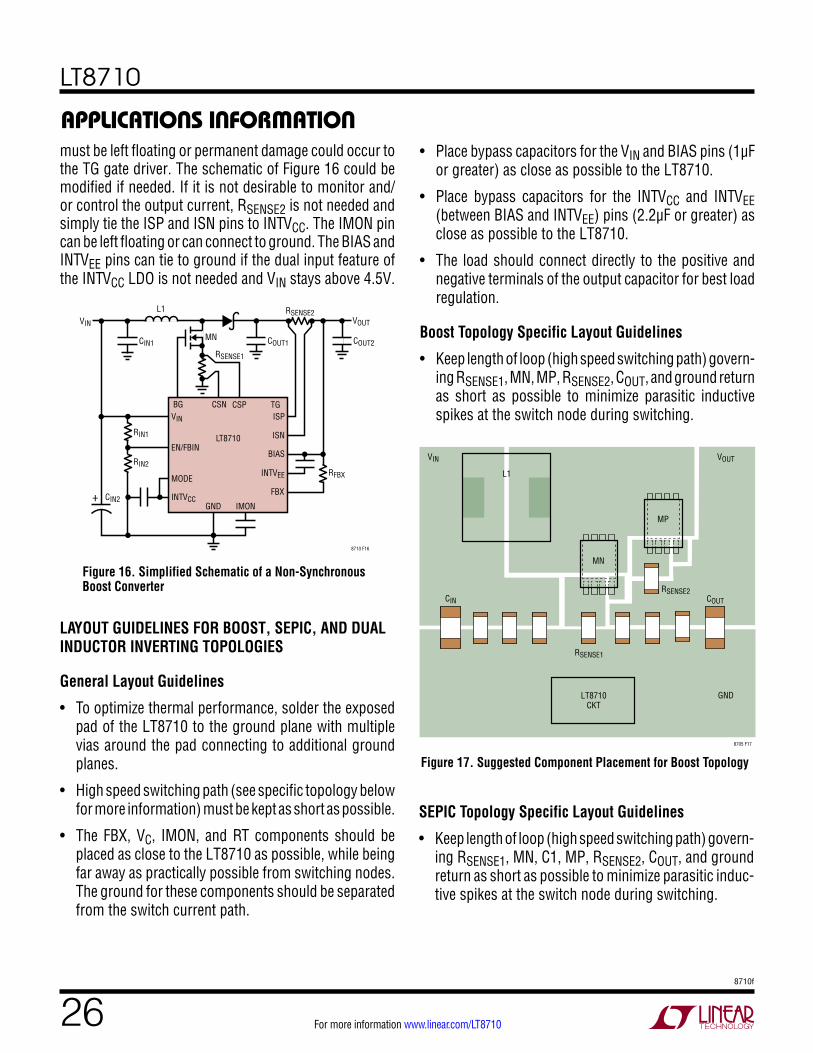
LT8710
268710f
For more information www.linear.com/LT8710
must be left floating or permanent damage could occur to the TG gate driver. The schematic of Figure 16 could be modified if needed. If it is not desirable to monitor and/or control the output current, RSENSE2 is not needed and simply tie the ISP and ISN pins to INTVCC. The IMON pin can be left floating or can connect to ground. The BIAS and INTVEE pins can tie to ground if the dual input feature of the INTVCC LDO is not needed and VIN stays above 4.5V.
• Place bypass capacitors for the VIN and BIAS pins (1µF or greater) as close as possible to the LT8710.
• Place bypass capacitors for the INTVCC and INTVEE (between BIAS and INTVEE) pins (2.2µF or greater) as close as possible to the LT8710.
• The load should connect directly to the positive and negative terminals of the output capacitor for best load regulation.
Boost Topology Specific Layout Guidelines
• Keep length of loop (high speed switching path) govern-ing RSENSE1, MN, MP, RSENSE2, COUT, and ground return as short as possible to minimize parasitic inductive spikes at the switch node during switching.
applicaTions inForMaTion
Figure 17. Suggested Component Placement for Boost Topology
Figure 16. Simplified Schematic of a Non-SynchronousBoost Converter
LAYOUT GUIDELINES FOR BOOST, SEPIC, AND DUAL INDUCTOR INVERTING TOPOLOGIES
General Layout Guidelines
• To optimize thermal performance, solder the exposed pad of the LT8710 to the ground plane with multiple vias around the pad connecting to additional ground planes.
• High speed switching path (see specific topology below for more information) must be kept as short as possible.
• The FBX, VC, IMON, and RT components should be placed as close to the LT8710 as possible, while being far away as practically possible from switching nodes. The ground for these components should be separated from the switch current path.
IMONGND
CSP TGCSNBG
LT8710
8710 F16
MODE
INTVCC
VIN
EN/FBINBIAS
INTVEE
FBX
ISP
ISN
VOUT VIN
RIN1
L1
CIN2
RIN2
RSENSE2
RSENSE1
MNCIN1
RFBX
COUT2
+
COUT1
SEPIC Topology Specific Layout Guidelines
• Keep length of loop (high speed switching path) govern-ing RSENSE1, MN, C1, MP, RSENSE2, COUT, and ground return as short as possible to minimize parasitic induc-tive spikes at the switch node during switching.
MN
LT8710CKT
L1
RSENSE1
RSENSE2
8705 F17
VIN
CIN
VOUT
COUT
GND
MP

LT8710
278710f
For more information www.linear.com/LT8710
applicaTions inForMaTion
Figure 18. Suggested Component Placement for SEPIC Topology
Figure 19. Suggested Component Placement for Dual Inductor Inverting Topology
Figure 20. Suggested Routing and Connections of CSP/CSN and ISP/ISN Lines
THERMAL CONSIDERATIONS
Overview
The primary components on the board that consume the most power and produce the most heat are the power switches, MN and MP, the power inductor, and the LT8710 IC. It is imperative that a good thermal path be provided for these components to dissipate the heat generated within the packages. This can be accomplished by taking advantage of the thermal pads on the underside of the packages. It is recommended that multiple vias in the printed circuit board be used to conduct heat away from each of these components and into a copper plane with as much area as possible. For the case of the power switches, the copper area of the drain connections shouldn’t be too big as to create a large EMI surface that can radiate noise around the board.
Dual Inductor Inverting Topology Specific Layout Guidelines
• Keep ground return path from the low side of RSENSE1 and RSENSE2 (to chip) separated from CIN’s and COUT’s ground return path (to chip) in order to minimize switch-ing noise coupling into the input and output. Notice the cuts in the ground return for the low side of RSENSE1 and RSENSE2.
• Keep length of loop (high speed switching path) govern-ing RSENSE1, MN, C1, MP, RSENSE2, and ground return as short as possible to minimize parasitic inductive spikes at the switch node during switching.
Current Sense Resistor Layout Guidelines
• Route the CSP/CSN and ISP/ISN lines differentially (close together) from the chip to the current sense resistor as shown in Figure 20.
• Place the vias that connect the CSP/CSN and ISP/ISN lines directly at the terminals of the current sense resis-tor as shown in Figure 20.
8705 F18
LT8710CKT
GND
MN
MP
L1 L2
RSENSE1
RSENSE2
VIN C1
CIN
VOUT
COUT
•
•
8705 F19
LT8710CKT GND
CIN COUT
RSENSE1 RSENSE2
R1
D1
C2
C1
MPMN
VIN VOUTL1 L2
•
•
8705 F20
RSENSE1, 2
TOCURRENT
SENSEPINS

LT8710
288710f
For more information www.linear.com/LT8710
applicaTions inForMaTionPower MOSFET Loss and Thermal Calculations
The LT8710 requires two external power MOSFETs, an NFET switch for the BG gate driver and a PFET switch for the TG gate driver. Important parameters for estimating the power dissipation in the MOSFETs are:
1. On-resistance (RDSON)
2. Gate-to-drain charge (QGD)
3. PFET body diode forward voltage (VBD)
4. VDS of the FETs during their Off-Time
5. Switch current (ISW)
6. Switching frequency (f)
The power loss in each power switch has a DC and AC term. The DC term is when the power switch is fully on, and the AC term is when the power switch is transitioning from on-off or off-on.
The following applies for both the NFET and PFET power switches. For a boost application, the average current through the MOSFET (ISW) during its on-time, is the same as the average input current. The magnitude of the drain-to-source voltage, VDS, during its off-time is approximately VOUT. For a SEPIC or dual inductor inverting application, the average current through each MOSFET (ISW) during its on-time, is the sum of the average input current and the output current. The |VDS| voltage during the off-time is approximately VIN + |VOUT|. During the non-overlap time of the gate drivers, the peak and valley inductor current is flowing through the body diode of the PFET. Below are the equations for the power loss in MN and MP.
P PMOSFET I2R PSWI CHT INGPMN=
=IN2 •RDS N+ +VDS •IN • f • tRF PRR –N
PMP =IP2 •RDSO
O
N+VBD• IPK+
+
IVY1.6 • f•140ns+PRR –P
ISW =IOUT
(1–DC); IPK =ISW+
+
iRIPPLE2
; IVY =ISW –iRIPPLE
2
IN= DC • ISW 2 iRIPPLE2
12
IP = 1–DC( ) •
+ISW 2 iRIPPLE2
12
PRR –N≈VDS •IRR • tRR • f
P
2
2RR –P ≈VDS •IRR • tRR • f
where:
f = Switching Frequency
IN = NFET RMS Current
IP = PFET RMS Current
tRF = Average of the rise and fall times of the NFET’s drain voltage
ISW = Average switch current during its on-time
IPK = Peak inductor current
IVY = Valley inductor current
iRIPPLE = Inductor ripple current
DC = Switch duty cycle (see Power Switch Duty Cycle section in Appendix)
VBD = PFET body diode forward voltage at ISW
VDS = Voltage across the FET when it’s off. VOUT for a boost, VIN + |VOUT| for a dual inductor inverting or SEPIC converter
PRR-N = PFET body diode reverse recovery power loss in the NFET
PRR-P = PFET body diode reverse recovery power loss in the PFET
LT8710
298710f
For more information www.linear.com/LT8710
applicaTions inForMaTionIRR = Current needed to remove the PFET body diode charge
tRR = Reverse recovery time of PFET body diode
Typical values for tRF are 10ns to 40ns depending on the MOSFET capacitance and drain voltage. In general, the lower the QGD of the MOSFET, the faster the rise and fall times of its drain voltage. For best calculations, measure the rise and fall times in the application.
PFET body diode reverse recovery power loss is depen-dent on many factors and can be difficult to quantify in an application. In general, this power loss increases with higher VDS and/or higher switching frequency.
Chip Power and Thermal Calculations
Power dissipation in the LT8710 chip comes from three primary sources: INTVCC and INTVEE LDOs providing gate drive to the BG and TG pins and additional input quiescent current. The average current through each LDO is deter-mined by the gate charge of the power switches, MN and MP, and the switching frequency. Below are the equations for calculating the chip power loss followed by examples.
Noninverting Converter: The INTVCC LDO primarily sup-plies voltage for the BG gate driver. The BIAS and INTVEE voltages supply the top and bottom rails of the TG gate driver respectively. The chip Q current comes from the higher of VIN and BIAS. Below are the chip power equa-tions for a noninverting converter:
PVCC = 1.04 • QMN • f • VSELECT PVEE1 = QMP • f • VBIAS PVEE2 = 3.1mA • (1 – DC) • VBIAS PQ = 4mA • VMAX
where:
f = Switching frequency
DC = Switch duty cycle (see Power Switch Duty Cycle section in Appendix)
QMN = Total gate charge of NFET power switch (MN) at 6.3VGS
QMP = Total gate charge of PFET power switch (MP) at 6.18VSG
VSELECT = INTVCC LDO selected input voltage, VIN or BIAS (see LDO REGULATORS section)
VMAX = Higher of VIN and BIAS.
Inverting Converter: Due to BIAS connecting to INTVCC and INTVEE connecting to ground (see Typical Applica-tions), all the chip power comes from the VIN pin. The INTVCC LDO primarily supplies voltage for both the BG and TG gate drivers. The chip Q current comes from VIN. For consistency, the power that’s needed to run the TG gate driver is still labeled as PVEE even though the power is coming from INTVCC. Below are the chip power equations for an inverting converter: PVCC = 1.04 • QMN • f • VIN PVEE1 = QMP • f • VIN PVEE2 = 3.15mA • (1 – DC) • VIN PQ = 5.5mA • VIN
where:
f = Switching frequency
DC = Switch duty cycle (see Power Switch Duty Cycle section in Appendix)
QMN = Total gate charge of NFET power switch (MN) at 6.3VGS
QMP = Total gate charge of PFET power switch (MP) at 6.3VSG
Chip Power Calculations Example
Table 4 calculates the power dissipation of the LT8710 for a 200kHz, 3V – 40V to 5V SEPIC application when VIN is 12V. From PCHIP in Table 4, the die junction temperature can be calculated using the appropriate thermal resistance and worst-case ambient temperature:
TJ = TA + QJA • PCHIP
where TJ = die junction temperature, TA = ambient tem-perature and θJA is the thermal resistance from the silicon junction to the ambient air.
The published θJA value is 38°C/W for the TSSOP exposed pad package. In practice, lower θJA values are realizable if board layout is performed with appropriate grounding

LT8710
308710f
For more information www.linear.com/LT8710
applicaTions inForMaTion
Table 4. Power Calculations Example for a 200kHz, 3V to 40V to 5V/5A SEPIC (VIN = 12V, MN = FDMS86500L and MP = SUD50P06-15)DEFINITION OF VARIABLES EQUATION DESIGN EXAMPLE VALUE
DC = Switch Duty Cycle
DC ≅ VOUT
VIN+ VOUT DC ≅ 5V
12V +5V DC ≅ 29.4%
PVCC = INTVCC LDO Power Driving the BG Gate DriverQMN = NFET Total Gate Charge at VGS = 6.3Vf = Switching FrequencyVSELECT = LDO Chooses VIN
PVCC = 1.04 • QMN • f • VSELECT PVCC = 1.04 • 73nC • 200kHz • 12V PVCC = 182.2mW
PVEE1 = INTVEE LDO Power Driving the TG Gate DriverQMP = PFET Total Gate Charge at VSG = 4.25V
PVEE1 = QMP • f • VBIAS PVEE1 = 55nC • 200kHz • 5V PVEE1 = 55mW
PVEE2 = Additional TG Gate Driver Power Loss
PVEE2 = 3.1mA • (1 – DC) • VBIAS PVEE2 = 3.1mA • (1– 0.294) • 5V PVEE2 = 10.9mW
PQ = Chip Bias Loss VMAX = Higher Voltage of VIN and BIAS
PQ = 4mA • VMAX PQ = 4mA • 12V PQ = 48mW
PCHIP = 296.1mW
(accounting for heat sinking properties of the board) and other considerations listed in the Layout Guidelines sec-tion. For instance, a θJA value of ~22°C/W was consistently achieved when board layout was optimized as per the suggestions in the Layout Guidelines section.
Thermal Lockout
If the die temperature reaches ~175°C, the part will go into reset, so the power switches turn off and the soft-start capacitor will be discharged. The LT8710 will come out of reset when the die temperature drops by ~5°C (typical).

LT8710
318710f
For more information www.linear.com/LT8710
appenDixPOWER SWITCH DUTY CYCLE
In order to maintain loop stability and deliver adequate current to the load, the external power NFET (MN in the Block Diagram) cannot remain on for 100% of each clock cycle. The maximum allowable duty cycle is given by:
DCMAX =
TP –MinOffTime( )TP
•100%
where TP is the clock period and MinOffTime (found in the Electrical Characteristics) is a maximum of 480ns.
Conversely, the external power NFET (MN in the Block Diagram) cannot remain off for 100% of each clock cycle, and will turn on for a minimum on time (MinOnTime) when in regulation. This MinOnTime governs the minimum al-lowable duty cycle given by:
DCMIN =
(MinOnTime)TP
•100%
where TP is the clock period and MinOnTime (found in the Electrical Characteristics) is a maximum of 420ns.
The application should be designed such that the operating duty cycle is between DCMIN and DCMAX.
Duty cycle equations for several common topologies are given below where VON_MP is the voltage drop across the external power PFET (MP) when it is on, and VON_MN is the voltage drop across the external power NFET (MN) when it is on.
For the boost topology (see Figure 5):
DCBOOST ≅
VOUT – VIN+ VON_MPVOUT+ VON_MP – VON_MN
For the SEPIC or dual inductor inverting topology (see Figures 6 and 7):
DCSEPIC_&_INVERT ≅ | VOUT|+VON_MP
VIN+|VOUT|+VON_MP – VON_MN
The LT8710 can be used in configurations where the duty cycle is higher than DCMAX, but it must be operated in the discontinuous conduction mode (MODE pin must be high) so that the effective duty cycle is reduced.
INDUCTOR SELECTION
For high efficiency, choose inductors with high frequency core material, such as ferrite, to reduce core losses. Also to improve efficiency, choose inductors with more volume for a given inductance. The inductor should have low DCR (copper-wire resistance) to reduce I2R losses, and must be able to handle the peak inductor current without saturat-ing. Note that in some applications, the current handling requirements of the inductor can be lower, such as in the SEPIC topology where each inductor carries a fraction of the total switch current. Molded chokes or chip inductors do not have enough core area to support peak inductor currents in the 5A to 15A range. To minimize radiated noise, use a toroidal or shielded inductor. See Table 5 for a list of inductor manufacturers.
Table 5. Inductor ManufacturersCoilcraft MSS1278, XAL1010, and
MSD1278 Serieswww.coilcraft.com
Cooper Bussmann
DRQ127, DR127, and HCM1104 Series
www.cooperbussmann.com
Vishay IHLP Series www.vishay.com
Würth WE-DCT Series WE-CFWI Series
www.we-online.com
Minimum Inductance
Although there can be a trade-off with efficiency, it is often desirable to minimize board space by choosing smaller inductors. When choosing an inductor, there are three conditions that limit the minimum inductance; (1) providing adequate load current, and (2) avoidance of subharmonic oscillation, and (3) supplying a minimum ripple current to avoid false tripping of the current comparator.

LT8710
328710f
For more information www.linear.com/LT8710
appenDixAdequate Load Current
Small value inductors result in increased ripple currents and thus, due to the limited peak switch current, decrease the average current that can be provided to the load. In order to provide adequate load current, L should be at least:
LBOOST ≥VIN •DC
2 • f •VCSPN
RSENSE1–
VOUT •IOUTVIN •η
or
LDUAL ≥VIN •DC
2 • f •VCSPN
RSENSE1–
|VOUT|•IOUTVIN •η
–IOUT
where:
LBOOST = L1 for boost topologies (see Figure 5)
LDUAL = L1 = L2 for coupled dual inductor topologies (see Figures 6 and 7)
LDUAL = L1 || L2 for uncoupled dual inductor topolo- gies (see Figures 6 and 7)
DC = Switch duty cycle (see previous section)
VCSPN = Current limit voltage at the operating switch duty cycle (see Max Current Limit vs Duty Cycle (CSP – CSN) plot in the Typical Per- formance Characteristics)
RSENSE1 = Current sense resistor connected across the CSP-CSN pins (see Block Diagram)
η = Power conversion efficiency (assume 90%)
f = Switching frequency
IOUT = Maximum output current
Negative values of LBOOST or LDUAL indicate that the out-put load current, IOUT, exceeds the switch current limit capability of the converter. Decrease RSENSE1 to increase the switch current limit.
Avoiding Subharmonic Oscillations
The LT8710’s internal slope compensation circuit will prevent subharmonic oscillations that can occur when the duty cycle is greater than 50%, provided that the in-ductance exceeds a minimum value. In applications that operate with duty cycles greater than 50%, the inductance must be at least:
LMIN ≥
VIN •RSENSE1•(2 •DC–1)40m •DC • f •(1–DC)
where
LMIN = L1 for boost topologies (see Figure 5)
LMIN = L1 = L2 for coupled dual inductor topologies (see Figures 6 and 7)
LMIN = L1 || L2 for uncoupled dual inductor topologies (see Figures 6 and 7)
Maximum Inductance
Excessive inductance can reduce ripple current to levels that are difficult for the current comparator (A5 in the Block Diagram) to cleanly discriminate, thus causing duty cycle jitter and/or poor regulation. The maximum inductance can be calculated by:
LMAX ≤
VIN •RSENSE1•DC5m • f
where:
LMAX = L1 for boost topologies (see Figure 5)
LMAX = L1 = L2 for coupled dual inductor topologies (see Figures 6 and 7)
LMAX = L1 || L2 for uncoupled dual inductor topologies (see Figures 6 and 7)
Inductor Current Rating
The inductor(s) must have a rating greater than its (their) peak operating current to prevent inductor saturation, which would result in efficiency losses. The maximum
Boost Topology
SEPIC or Inverting Topologies

LT8710
338710f
For more information www.linear.com/LT8710
appenDixinductor current (considering start-up and steady-state conditions) is given by:
IL_PEAK =
54mV –16mV •DC2
RSENSE1+
VIN • TMIN_PROPL
where
IL_PEAK = Peak inductor current in L1 for a boost topology, or the sum of the peak inductor currents for dual inductor topologies.
TMIN_PROP = 100ns (propagation delay through the current feedback loop).
For wide input voltage range applications, as the input volt-age increases, the max peak inductor current also increases due to the duty cycle decreasing. It is recommended to utilize the output current limiting feature to reduce the max peak inductor current given by the following equation:
IL_PEAK =
VISPNRSENSE2 •(1–DC)
+VIN •DC2 • f •L
where….
VISPN = 57mV max for noninverting converters and 60mV max for inverting converters.
Note that these equations offer conservative results for the required inductor current ratings. The current ratings could be lower for applications with light loads, and if the SS capacitor is sized appropriately to limit inductor currents at start-up.
POWER MOSFET SELECTION
The LT8710 requires two external power MOSFETs, an NFET switch for the BG gate driver and a PFET switch for the TG gate driver. It is important to select MOSFETs for optimizing efficiency. For choosing an NFET and PFET, the important device parameters are:
1. Breakdown voltage (BVDSS)
2. Gate threshold voltage (VGSTH)
3. On-resistance (rDSON)
4. Total gate charge (QG)
5. Turn-off delay time (tD(OFF))
6. Package has exposed paddle
The drain-to-source breakdown voltage of the NFET and PFET power MOSFETs must exceed:
• BVDSS > VOUT for boost converter
• BVDSS > VIN+|VOUT| for SEPIC or dual inductor inverting converter
If operating close to the BVDSS rating of the MOSFET, check the leakage specifications on the MOSFET because leakage can decrease the efficiency of the converter.
The NFET and PFET gate-to-source drive is approximately 6.3V and 6.18V respectively, so logic level MOSFETs are required. The BG gate driver can begin switching when the INTVCC voltage exceeds ~4V, so ensure the selected NFET is in the linear mode of operation with 4V of gate-to-source drive to prevent possible damage to the NFET.
The TG gate driver can begin switching when the BIAS-INTVEE voltage exceeds ~3.42V, so it is optimal that the PFET be in the linear mode of operation with 3.42V of gate-to-source drive. However, the PFET is less likely to get damaged if it’s not operating in the linear region since the drain-to-source voltage is clamped by its body diode during the NFET’s off-time. Having said that, try to choose a PFET with a low body diode reverse recovery time to minimize stored charge in the PFET. The stored charge in the PFET body diode gets removed when the NFET switch turns on and can lead to efficiency hits especially in ap-plications where the VDS of the PFET (during off-time) is high. For these applications, it may be beneficial to put a Schottky diode across the PFET to reduce the amount of charge in the PFET body diode. In applications where the output voltage is high in magnitude, it may be better to replace the PFET with a Schottky diode since the converter may be more efficient with a Schottky.
Power MOSFET on-resistance and total gate charge go hand-in-hand and are typically inversely proportional to each other; the lower the on-resistance, the higher total gate charge. Choose MOSFETs with an on-resistance to give a voltage drop to be less than 300mV at the peak

LT8710
348710f
For more information www.linear.com/LT8710
appenDixcurrent. At the same time, choose MOSFETs with a lower total gate charge to reduce LT8710 power dissipation and MOSFET switching losses.
The turn-off delay time (tD(OFF)) of available NFETs is generally smaller than the LT8710’s non-overlap time. However, the turn-off time of the available PFETs should be looked at before deciding on a PFET for a given applica-tion. The turn-off time must be less than the non-overlap time of the LT8710 or else the NFET and PFET could be on at the same time and damage to external components may occur. If the PFET turn-off delay time as specified in the data sheet is less than the LT8710 non-overlap time, then the PFET is good to use. If the turn-off delay time is longer than the non-overlap time, it doesn’t necessarily mean it can’t be used. It may be unclear how the PFET manufacturer measures the turn-off delay time, so it is best to measure the PFET turn-off delay time with respect to the PFET gate voltage.
Finally, both the NFET and PFET power MOSFETs should be in a package with an exposed paddle for the drain connection to be able to dissipate heat. The on-resistance of MOSFETs is proportional to temperature, so it’s more efficient if the MOSFETs are running cool with the help of the exposed paddle. See Table 6 for a list of power MOSFET manufacturers.
Table 6. Power MOSFET (NFET and PFET) ManufacturersFairchild Semiconductor www.fairchildsemi.com
On-Semiconductor www.onsemi.com
Vishay www.vishay.com
Diodes Inc. www.diodes.com
INPUT AND OUTPUT CAPACITOR SELECTION
Input and output capacitance is necessary to suppress voltage ripple caused by discontinuous current moving in and out of the regulator. A parallel combination of ca-pacitors is typically used to achieve high capacitance and low ESR (equivalent series resistance). Tantalum, special polymer, aluminum electrolytic and ceramic capacitors are all available in surface mount packages. Capacitors with low ESR and high ripple current ratings, such as OS-CON and POSCAP are also available.
Ceramic capacitors should be placed near the regulator input and output to suppress high frequency switching noise. A minimum 1µF ceramic capacitor should also be placed from VIN to GND and from BIAS to GND as close to the LT8710 pins as possible. Due to their excellent low ESR characteristics, ceramic capacitors can significantly reduce ripple voltage and help reduce power loss in the higher ESR bulk capacitors. X5R or X7R dielectrics are preferred, as these materials retain their capacitance over wide voltage and temperature ranges. Many ceramic ca-pacitors, particularly 0805 or 0603 case sizes, have greatly reduced capacitance at the desired operating voltage.
Input Capacitor, CIN
The input capacitor, CIN, sees the ripple current of the input inductor, L1, which eases the capacitance requirements of CIN. Below is the equation for calculating the capacitance of CIN for 0.5% input voltage ripple:
CIN >
DC8 •L • f2 •0.005
where:
DC = Switch duty cycle (see Power Switch Duty Cycle section)
L = LBOOST or LDUAL (see Inductor Selection section)
f = Switching frequency
The worst-case for the input capacitor (largest capacitance needed) is when the input voltage is at its lowest because the duty cycle is the highest. Keep in mind that the volt-age rating of the input capacitor needs to be greater than the maximum input voltage. This equation calculates the capacitance value during steady-state operation and may need to be adjusted for desired transient response. Also, this assumes no ESR, so the input capacitance may need to be larger depending on the equivalent ESR of the input capacitor(s).
Output Capacitor, COUT
The output capacitor, COUT, in a boost or SEPIC topology has chopped current flowing through it, whereas the output capacitor in a dual inductor inverting topology sees the

LT8710
358710f
For more information www.linear.com/LT8710
appenDixinductor ripple current. Below is the equation for calculating the capacitance of COUT for 0.5% output voltage ripple:
COUT >
IOUT •DCf •0.005 • VOUT
or
COUT >
1–DC8 •L • f2•0.005
where:IOUT = Maximum output current of converterDC = Switch duty cycle (see Power Switch Duty Cycle section)L = LBOOST or LDUAL (see Inductor Selection section)
f = Switching frequency
The worst-case for the output capacitor (largest capacitance needed) is when the output regulation voltage is relatively low. This equation calculates the capacitance value during steady-state operation and may need to be adjusted for desired transient response. Also, this assumes no ESR, so the output capacitance may need to be larger depending on the equivalent ESR of the output capacitor(s). See Table 7 for a list of ceramic capacitor manufacturers.
Table 7. Ceramic Capacitor ManufacturersTDK www.tdk.comMurata www.murata.comTaiyo Yuden www.t-yuden.com
COMPENSATION – ADJUSTMENT
To compensate the feedback loop of the LT8710, a series resistor capacitor network in parallel with an optional single capacitor should be connected from the VC pin to GND. For most applications, choose a series capacitor in the range of 1nF to 10nF with 4.7nF being a good starting value. The optional parallel capacitor should range in value from 47pF to 220pF with 100pF being a good starting value. The compensation resistor, RC, is usually in the range of 5k to 50k. A good technique to compensate a new application is to use a 100k potentiometer in place of the series resistor RC. With the series and parallel capacitors at 4.7nF and 100pF respectively, adjust the potentiometer while observing the transient response and Figure 21c. Transient Response is Well Damped
Figure 21a. Transient Response Shows Excessive Ringing
Figure 21b. Transient Response is Better
the optimum value for RC can be found. The series capaci-tor can be reduced or increased from 4.7nF to speed up the converter or slow down the converter, respectively. For the circuit in Figure 7, a 3.3nF series cap was used. Figures 21a to 21c illustrate this process for the circuit of Figure 7 with a load current stepped between 2A and 5.5A with an input voltage of 9V. Figure 21a shows the transient response with RC equal to 1k. The phase mar-gin is poor as evidenced by the excessive ringing in the output voltage and inductor current. In Figure 21b, the value of RC is increased to 4k, which results in a more damped response. Figure 21c shows the results when RC is increased further to 11.5k. The transient response is nicely damped and the compensation procedure is complete.
Dual Inductor Inverting Topology
Boost or SEPIC Topologies
8705 F21a
VOUT200mV/DIV
AC-COUPLED
LOAD STEP5A/DIV
IL1 + IL25A/DIV
RC = 1k200µs/DIV
8705 F21b
VOUT200mV/DIV
AC-COUPLED
LOAD STEP5A/DIV
IL1 + IL25A/DIV
RC = 4k200µs/DIV
8705 F21c
VOUT200mV/DIV
AC-COUPLED
LOAD STEP5A/DIV
IL1 + IL25A/DIV
RC = 11.5k200µs/DIV

LT8710
368710f
For more information www.linear.com/LT8710
appenDixCOMPENSATION – THEORY
Like all other current mode switching regulators, the LT8710 needs to be compensated for stable and efficient operation. Two feedback loops are used in the LT8710: a fast current loop which does not require compensation, and a slower voltage loop which does. Standard bode plot analysis can be used to understand and adjust the voltage feedback loop.
As with any feedback loop, identifying the gain and phase contribution of the various elements in the loop is critical. Figure 22 shows the key equivalent elements of a boost converter. Because of the fast current control loop, the power stage of the IC, inductor and PFET have been re-placed by a combination of the equivalent transconductance amplifier gmp and the current controlled current source
(which converts IVIN to
ηVINVOUT
IVIN ). Gmp acts as a current source where the peak input current, IVIN, is proportional to the VC voltage and current sense resistor, RSENSE1.
Figure 22. Boost Converter Equivalent Model
Note that the maximum output currents of gmp and gma are finite. The external current sense resistor, RSENSE1, sets the value of:
gmp ≈
16 •RSENSE1
The error amplifier, gma, is nominally about 200µmhos with a source and sink current of about 12µA and 19µA respectively.
From Figure 22, the DC gain, poles and zeros can be calculated as follows:
DC GAIN:
ADC =gma •RO •gmp • η•VIN
VOUT•RL2
•0.5 •R2
RFBX +0.5 •R2
Output Pole:P1=2
2 • π •RL •COUT
Error AmpPole:P2=1
2 • π •(RO+RC)•CC
Error Amp Zero: Z1=1
2 • π •RC•CC
ESR Zero: Z2=1
2 • π •RESR •COUT
RHP Zero: Z3=VIN2 •RL
2 • π • VOUT2 •L
HighFrequency Pole:P3>fS3
Phase Lead Zero: Z4=1
2 • π •RFBX •CPL
Phase LeadPole:P4=1
2 • π •RFBX •0.5 •R2RFBX +0.5 •R2
•CPL
Error AmpFilter Pole:P5=1
2 • π •RC •RORC+RO
•CF
,CF <CC10
The current mode zero (Z3) is a right half plane zero which can be an issue in feedback control design, but is manageable with proper external component selection.
8710 F22
CC: COMPENSATION CAPACITORCOUT: OUTPUT CAPACITORCPL: PHASE LEAD CAPACITORCF: HIGH FREQUENCY FILTER CAPACITORgma: TRANSCONDUCTANCE AMPLIFIER INSIDE ICgmp: POWER STAGE TRANSCONDUCTANCE AMPLIFIERRC: COMPENSATION RESISTORRL: OUTPUT RESISTANCE DEFINED AS VOUT/ILOADMAXRO: OUTPUT RESISTANCE OF gmaR2, RFBX: FEEDBACK RESISTOR DIVIDER NETWORK RESR: OUTPUT CAPACITOR ESRη: CONVERTER EFFICIENCY (~90% AT HIGHER CURRENTS)
IVIN
CPL
CF
–
+
–
+
1.213VREFERENCE
CC
RC RO
VC R2
RFBX
VOUT
RL
R2
FBXgma
gmp
η • VINVOUT
• IVIN
RESR
COUT
RL

LT8710
378710f
For more information www.linear.com/LT8710
appenDixUsing the circuit in Figure 24 with a 4A load as an example, Table 9 shows the parameters used to generate the bode plot shown in Figure 23.
Table 9: Bode Plot ParametersPARAMETER VALUE UNITS COMMENT
RL 3 Ω Application Specific
COUT 88 µF Application Specific
RESR 2 mΩ Application Specific
RO 350 kΩ Not Adjustable
CC 3300 pF Adjustable
CF 100 pF Optional/Adjustable
CPL 0 pF Optional/Adjustable
RC 18 kΩ Adjustable
RFBX 130 kΩ Adjustable
R2 14.5 kΩ Not Adjustable
VOUT 12 V Application Specific
VIN 5 V Application Specific
gma 200 µmho Not Adjustable
gmp 167 mho Application Specific
L 1.3 µH Application Specific
fOSC 400 kHz Adjustable
Figure 23. Bode Plot for Example Boost Converter
From Figure 23, the phase is –135° when the gain reaches 0dB giving a phase margin of 45°. The crossover fre-quency is 20kHz, which is about three times lower than the frequency of the RHP zero Z3 to achieve adequate phase margin.
Figure 24. 5V to 12V Boost Converter
IMON SSGND
CSP TGCSNBG
LT8710
8710 F24
MODE
INTVCC
RT
SYNC
VIN
EN/FBIN BIAS
INTVEE
FBX
FLAG
VC
ISP
ISN
VOUT 12V6A
VIN5V
RIN113.3k
L11.3µH
CIN2330µF
2.2µF
COUT22µF×4
RIN210kCIN1
22µF×4
RT88.7k
1m
RSENSE25m
MN×2
MP
RSENSE1
RFBX130k
RC18k
2.2µF
CIMON47nF
CSS220nF
CC3.3nF
CF100pF
+
FREQUENCY (Hz)GA
IN (d
B)
PHASE (DEG)
140
100
120
80
60
40
20
0
–20
0
–90
–45
–135
–180
–225
–270
–315
–36010 10k 100k 1M
8710 F23
100 1k
PHASE
GAIN45° AT20kHz

LT8710
388710f
For more information www.linear.com/LT8710
Typical applicaTion300kHz, 4.5V to 25V Input to –5V Output Delivers Up to 7A Output Current
Efficiency and Power LossTransient Response with 2A to 5.5A to 2A
Output Load Step (VIN = 12)
8710 TA02c
VOUT200mV/DIV
AC-COUPLED
LOAD STEP5A/DIV
IL1 + IL25A/DIV
200µs/DIV
CIN1: 10µF, 50V, 1210, X7SCIN2: OSCON 120µF, 35V, 35SVPF120MCOUT1: 100µF, 6.3V, 1812, X5RCOUT2: OSCON 330µF, 16V, 16SEQP330MC1: 10µF, 50V, 1210, X7S
L1, L2: WÜRTH 2.2µH WE-CFWI 74485540220MN: FAIRCHILD FDMS8333LMP: FAIRCHILD FDD4141RSENSE1: 1.5mΩ 2010RSENSE2: 4mΩ 2512D1: NXP PMEG2010EA
IMON SSGND
CSP TGCSNBG
LT8710
8710 TA02a
MODE
INTVCC
RT
SYNC
VIN
EN/FBINBIAS
INTVEE
FBX
FLAG
VC
ISN
ISP
VOUT –5V7A
VIN4.5V TO 25V
13.3k
L12.2µH
CIN2120µF
2.2µF
COUT1100µF×2
10k
CIN110µF×4
118k
1.5m
MN MP
RSENSE1
RSENSE24m
L22.2µH• •
C110µF ×2
60.4k
11.5k
2.2µFINTVCC
COUT2330µF+
47nF 220nF 3.3nF
100pF
+
499Ω D1
0.47µF
LOAD CURRENT (A)0
EFFI
CIEN
CY (%
)
POWER LOSS (W
)
100
80
90
70
65
50
40
30
20
8
6
7
5
4
3
2
1
01 4 5 6
8710 TA02b
72 3
VIN = 5VVIN = 12V

LT8710
398710f
For more information www.linear.com/LT8710
Typical applicaTion300kHz, SuperCap Backup Power
8710 TA03c
VIN10V/DIV
VOUT10V/DIV
VIMON1V/DIV
IL1 + IL25A/DIV
30s/DIV
8710 TA03d
VIN10V/DIV
VOUT10V/DIV
VIMON1V/DIV
IL1 + IL25A/DIV
30s/DIV
LOAD CURRENT (A)0
HOLD
-UP
TIM
E (s
)
200
150
175
125
100
75
50
25
00.5 1.5 2 2.5
8710 TA03b
31
VSYSTEM = 10.5VDURING HOLD-UP
System Hold-Up Time vsSystem Load Current
SuperCaps Charging When VIN Is Applied
SuperCaps Hold-Up System at 10.5V for ~83s When VIN Is Removed (ISYSTEM = 1A)
L1, L2: COILCRAFT 10µH MSD1278-103MLMN: FAIRCHILD FDMC8327LMP: VISHAY Si7611DNRSENSE1: 5mΩ 2010RSENSE2: 50mΩ 2512DIN: APPROPRIATE SCHOTTKY DIODE OR IDEALDIODE SUCH AS LTC4358, LTC4352, LTC4412, ETC.
CIN1: 22µF, 25V, 1812, X7RCOUT: 22µF, 25V, 1812, X7RC1: 10µF, 25V, 1210, X7RCS1-6: POWERSTOR HB1840-2R5606-RD1: CENTRAL SEMI CMDZ5245B-LTZ
IMON SSGND
CSP TGCSNBG
LT8710
8710 TA03a
MODE
INTVCC
RT
SYNC
VIN
EN/FBINBIAS
INTVEE
FBX
FLAG
VC
ISP
ISN
VOUT 15V
VIN12V ±5%
INPUT POWERSOURCE CAN BEREMOVED
DIN
49.9k
L1, 10µH
CIN2120µF
2.2µF10k
D115V
RT118k
5m
MN
MP
RSENSE1
L210µH
• C1, 10µF
165k
14.3k
47nF 220nF 2.2nF
100pF
+
CIN122µF×2
COUT22µF×2
•
RSENSE250m
VSYSTEM = VIN WHEN VIN IS PRESENT10.5V WHEN VIN IS REMOVED
1k
1.2k
1.2k
1.2k
1.2k
1.2k
1.2k
CS160F
+
CS260F
+
CS360F
+
CS460F
+
CS560F
+
CS660F
+
5.1Ω 5.1Ω
4.7nF 4.7nF
2.2µF

LT8710
408710f
For more information www.linear.com/LT8710
Typical applicaTion400kHz, 12V Boost Converter Delivers Up to 6A from a 4.5V to 9V Input
Efficiency and Power LossTransient Response with 2A to 5A to 2A
Output Load Step (VIN = 5V)
8710 TA04c
VOUT200mV/DIV
AC-COUPLED
LOAD STEP2A/DIV
IL1 + IL25A/DIV
200µs/DIV
L1: WÜRTH 1.3µH WE-HCI 7443551130MN: VISHAY SiR802DPMP: VISHAY Si7635DPRSENSE1: 1mΩ 2512RSENSE2: 5mΩ 2512
CIN1: 22µF, 16V, 1206, X5RCIN2: OSCON 330µF, 16V, 16SEQP330MCOUT1: 22µF, 25V, 1812, X7RCOUT2: OSCON 330µF, 16V, 16SEQP330M
IMON SSGND
CSP TGCSNBG
LT8710
8710 TA04a
MODE
INTVCC
RT
SYNC
VIN
EN/FBINBIAS
INTVEE
FBX
FLAG
VC
ISP
ISN
VOUT 12V6A
VIN4.5 TO 9V
13.3k
L11.3µH
COUT2330µF
2.2µF
10k
88.7k
1m
MN×2
MP
RSENSE1
130k
18k
2.2µF
47nF 220nF 3.3nF
100pF
+
RSENSE25m
COUT122µF×4
COUT2330µF
+CIN122µF×4
LOAD CURRENT (A)0
EFFI
CIEN
CY (%
)
POWER LOSS (W
)
100
80
90
70
60
50
40
30
20
8
6
7
5
4
3
2
1
01 4 5 6
8710 TA04b
2 3
VIN = 5VVIN = 8V

LT8710
418710f
For more information www.linear.com/LT8710
Typical applicaTion
Schematic and Equations for Calculating VOUT
VOUT Cleanly Transitions Through 0V with a 1V, 100Hz Sine Wave CNTL Signal (RLOAD = 2Ω)
Transient Response with Stepping VCNTL from 0V to –1V to 0V with 2Ω Output Load
300kHz, –5V to 5V Output Cleanly Transitions Through 0V with 3A Source and Sink Capability*
8710 TA05c
VCNTL1V/DIV
VOUT5V/DIV
IL1 + IL210A/DIV
5ms/DIV 8710 TA05d
VCNTL1V/DIV
VOUT5V/DIV
IL1 + IL210A/DIV
500µs/DIV
L1, L2: WÜRTH 4.4µH WE-CFWI 74485540440MN: FAIRCHILD FDMS8333LMP: FAIRCHILD FDD4141RSENSE1: 3mΩ 2010RSENSE2: 10mΩ 2512
* PATENT PENDING
CIN1: 22µF, 25V, 1812, X7RCIN2: OSCON 330µF, 16V, 16SEQP330MCOUT: 100µF, 6.3V, 1812, X5RC1: 10µF, 25V, 1210, X7RD1: CENTRAL SEMI CMPD1001
IMON SSGND
CSP TG
TG
CSNBG
LT8710
8710 TA05a
MODE
INTVCC
RT
SYNC
VIN
EN/FBINBIAS
INTVEE
FBX
FLAG
VC
ISP
ISP ISN
ISN
MP
TG
ISP
ISN
VOUT –5V TO 5V±3A
VIN
VCNTL
0V FOR VOUT = –5V–0.5V FOR VOUT = 0V–1V FOR VOUT = 5V
=
VIN11V TO
13V
L14.4µH
RSENSE1
MN
CIN2330µF
2.2µF
COUT100µF×3
CIN122µF×4
118k
3m
•
L24.4µH •
C110µF ×2
60.4k
D1
39.2k
2.2µF6.04k
10nF
47nF 220nF 2.2nF
100pF
+
RSENSE210m
FET BVDSS > 2VIN – VOUTCIVRATING > VIN – VOUT
DC =VIN – VOUT
2VIN – VOUT
FBX~9.6mV
RFBXRCNTL
VCNTL
VOUT
~83.1µA
8710 TA05b
LT8710
VOUT = 9.6mV –83.1µA • RFBX – (VCNTL – 9.6mV)RCNTL
RFBX
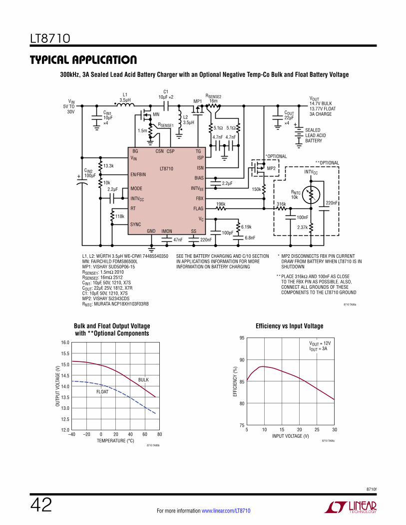
LT8710
428710f
For more information www.linear.com/LT8710
300kHz, 3A Sealed Lead Acid Battery Charger with an Optional Negative Temp-Co Bulk and Float Battery Voltage
Efficiency vs Input VoltageBulk and Float Output Voltagewith **Optional Components
Typical applicaTion
TEMPERATURE (°C)–40
OUTP
UT V
OLTA
GE (V
)
16.0
15.0
15.5
14.5
14.0
13.5
13.0
12.5
12.0–20 40 60 80
8710 TA06b
0 20
BULK
FLOAT
INPUT VOLTAGE (V)5
EFFI
CIEN
CY (%
)
95
90
85
80
7510 25 30
8710 TA06c
15 20
VOUT = 12VIOUT = 3A
L1, L2: WÜRTH 3.5µH WE-CFWI 74485540350MN: FAIRCHILD FDMS86500LMP1: VISHAY SUD50P06-15RSENSE1: 1.5mΩ 2010RSENSE2: 16mΩ 2512CIN1: 10µF, 50V, 1210, X7SCOUT: 22µF, 25V, 1812, X7RC1: 10µF, 50V, 1210, X7SMP2: VISHAY Si2343CDSRNTC: MURATA NCP18XH103F03RB
SEE THE BATTERY CHARGING AND C/10 SECTIONIN APPLICATIONS INFORMATION FOR MORE INFORMATION ON BATTERY CHARGING
* MP2 DISCONNECTS FBX PIN CURRENT DRAW FROM BATTERY WHEN LT8710 IS IN SHUTDOWN
** PLACE 316kΩ AND 100nF AS CLOSE TO THE FBX PIN AS POSSIBLE. ALSO, CONNECT ALL GROUNDS OF THESE COMPONENTS TO THE LT8710 GROUND
IMON SSGND
CSP TGCSNBG
LT8710
8710 TA06a
MODE
INTVCC
RT
SYNC
VIN
EN/FBINBIAS
INTVEE
FBX
FLAG
VC
ISP
ISN
VOUT 14.7V BULK13.77V FLOAT3A CHARGE
VIN5V TO
30V
13.3k
L13.5µH
RSENSE1
MN
CIN2100µF
2.2µF
COUT22µF×4
10k
CIN110µF×4
118k
1.5m
•
C110µF ×2
150k
*OPTIONAL
MP2
RNTC10k
INTVCC
196k 316k
6.19k
2.2µF
SEALEDLEAD ACIDBATTERY
47nF 220nF 6.8nF
100nF
100pF
+
L23.5µH
•
MP1
+
2.37k
220nF
**OPTIONAL
RSENSE216m
5.1Ω 5.1Ω
4.7nF 4.7nF

LT8710
438710f
For more information www.linear.com/LT8710
Information furnished by Linear Technology Corporation is believed to be accurate and reliable. However, no responsibility is assumed for its use. Linear Technology Corporation makes no representa-tion that the interconnection of its circuits as described herein will not infringe on existing patent rights.
FE20 (CB) TSSOP REV J 1012
0.09 – 0.20(.0035 – .0079)
0° – 8°
0.25REF
RECOMMENDED SOLDER PAD LAYOUT
0.50 – 0.75(.020 – .030)
4.30 – 4.50*(.169 – .177)
1 3 4 5 6 7 8 9 10
111214 13
6.40 – 6.60*(.252 – .260)
3.86(.152)
2.74(.108)
20 1918 17 16 15
1.20(.047)MAX
0.05 – 0.15(.002 – .006)
0.65(.0256)
BSC0.195 – 0.30
(.0077 – .0118)TYP
2
2.74(.108)
0.45 ±0.05
0.65 BSC
4.50 ±0.10
6.60 ±0.10
1.05 ±0.10
3.86(.152)
MILLIMETERS(INCHES) *DIMENSIONS DO NOT INCLUDE MOLD FLASH. MOLD FLASH
SHALL NOT EXCEED 0.150mm (.006") PER SIDE
NOTE:1. CONTROLLING DIMENSION: MILLIMETERS
2. DIMENSIONS ARE IN
3. DRAWING NOT TO SCALE
SEE NOTE 4
4. RECOMMENDED MINIMUM PCB METAL SIZE FOR EXPOSED PAD ATTACHMENT
6.40(.252)BSC
FE Package20-Lead Plastic TSSOP (4.4mm)
(Reference LTC DWG # 05-08-1663 Rev J)Exposed Pad Variation CB
package DescripTionPlease refer to http://www.linear.com/designtools/packaging/ for the most recent package drawings.
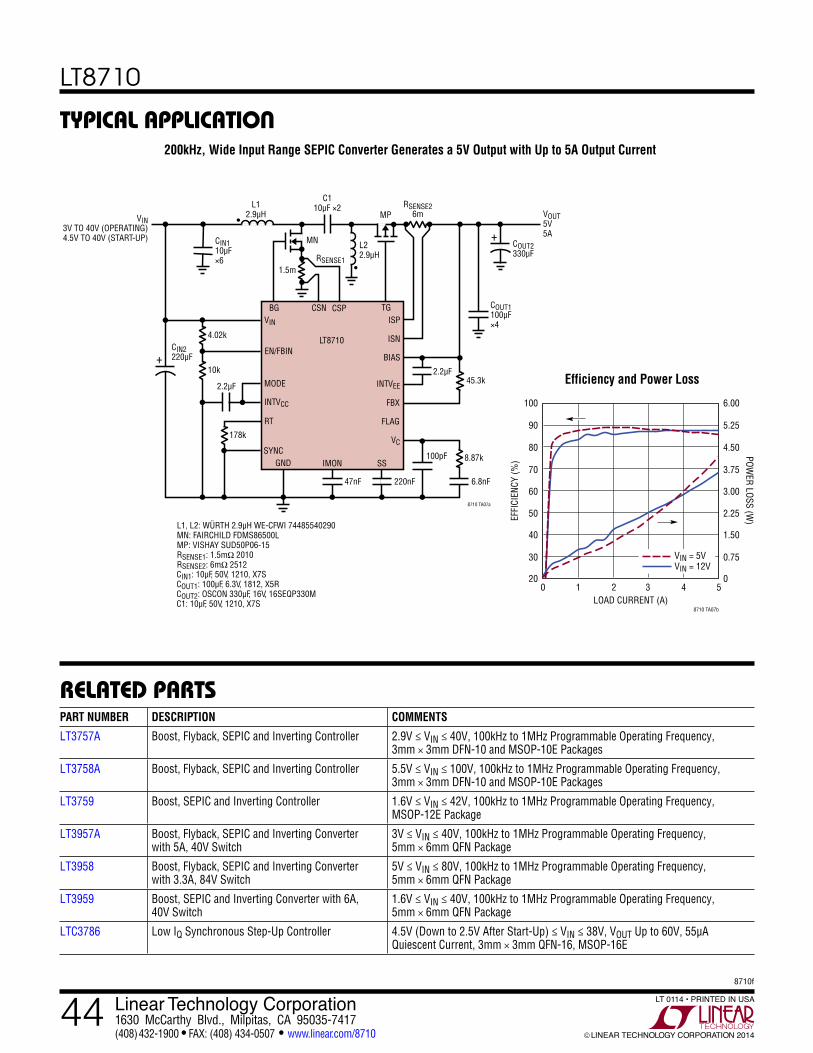
LT8710
448710f
For more information www.linear.com/LT8710
Linear Technology Corporation1630 McCarthy Blvd., Milpitas, CA 95035-7417(408) 432-1900 FAX: (408) 434-0507 www.linear.com/8710 LINEAR TECHNOLOGY CORPORATION 2014
LT 0114 • PRINTED IN USA
relaTeD parTs
Typical applicaTion
PART NUMBER DESCRIPTION COMMENTS
LT3757A Boost, Flyback, SEPIC and Inverting Controller 2.9V ≤ VIN ≤ 40V, 100kHz to 1MHz Programmable Operating Frequency, 3mm × 3mm DFN-10 and MSOP-10E Packages
LT3758A Boost, Flyback, SEPIC and Inverting Controller 5.5V ≤ VIN ≤ 100V, 100kHz to 1MHz Programmable Operating Frequency, 3mm × 3mm DFN-10 and MSOP-10E Packages
LT3759 Boost, SEPIC and Inverting Controller 1.6V ≤ VIN ≤ 42V, 100kHz to 1MHz Programmable Operating Frequency, MSOP-12E Package
LT3957A Boost, Flyback, SEPIC and Inverting Converter with 5A, 40V Switch
3V ≤ VIN ≤ 40V, 100kHz to 1MHz Programmable Operating Frequency, 5mm × 6mm QFN Package
LT3958 Boost, Flyback, SEPIC and Inverting Converter with 3.3A, 84V Switch
5V ≤ VIN ≤ 80V, 100kHz to 1MHz Programmable Operating Frequency, 5mm × 6mm QFN Package
LT3959 Boost, SEPIC and Inverting Converter with 6A, 40V Switch
1.6V ≤ VIN ≤ 40V, 100kHz to 1MHz Programmable Operating Frequency, 5mm × 6mm QFN Package
LTC3786 Low IQ Synchronous Step-Up Controller 4.5V (Down to 2.5V After Start-Up) ≤ VIN ≤ 38V, VOUT Up to 60V, 55µA Quiescent Current, 3mm × 3mm QFN-16, MSOP-16E
200kHz, Wide Input Range SEPIC Converter Generates a 5V Output with Up to 5A Output Current
Efficiency and Power Loss
L1, L2: WÜRTH 2.9µH WE-CFWI 74485540290MN: FAIRCHILD FDMS86500LMP: VISHAY SUD50P06-15RSENSE1: 1.5mΩ 2010RSENSE2: 6mΩ 2512CIN1: 10µF, 50V, 1210, X7SCOUT1: 100µF, 6.3V, 1812, X5RCOUT2: OSCON 330µF, 16V, 16SEQP330MC1: 10µF, 50V, 1210, X7S
IMON SSGND
CSP TGCSNBG
LT8710
8710 TA07a
MODE
INTVCC
RT
SYNC
VIN
EN/FBINBIAS
INTVEE
FBX
FLAG
VC
ISP
ISN
VOUT 5V5A
VIN3V TO 40V (OPERATING)4.5V TO 40V (START-UP)
4.02k
L12.9µH
CIN110µF×6
CIN2220µF
2.2µF
10k
178k
1.5m
MN
MP
RSENSE1
45.3k
8.87k
2.2µF
47nF 220nF 6.8nF
100pF
+
RSENSE26m
COUT1100µF×4
COUT2330µF
+
C110µF ×2
L22.9µH
•
•
LOAD CURRENT (A)0
EFFI
CIEN
CY (%
)
POWER LOSS (W
)
100
80
90
70
60
50
40
30
20
6.00
4.50
5.25
3.75
3.00
2.25
1.50
0.75
03 4 5
8710 TA07b
1 2
VIN = 5VVIN = 12V