Application of Nanostructures in Electrochromic …pakacademicsearch.com/pdf-files/eng/702/5029-5053...
25
Materials 2010, 3, 5029-5053; doi:10.3390/ma3125029 materials ISSN 1996-1944 www.mdpi.com/journal/materials Review Application of Nanostructures in Electrochromic Materials and Devices: Recent Progress Jinmin Wang 1 , Xiao Wei Sun 1,2, * and Zhihui Jiao 1 1 School of Electrical and Electronic Engineering, Nanyang Technological University, 50 Nanyang Avenue, Singapore 639798, Singapore; E-Mails: [email protected] (J.W.); [email protected] (Z.J.) 2 Department of Applied Physics, College of Science, Tianjin University, Tianjin 300072, China * Author to whom correspondence should be addressed; E-Mail: [email protected]; Tel.: +65-67905369; Fax: +65-67933318. Received: 18 October 2010; in revised form: 18 November 2010 / Accepted: 23 November 2010 / Published: 26 November 2010 Abstract: The recent progress in application of nanostructures in electrochromic materials and devices is reviewed. ZnO nanowire array modified by viologen and WO 3 , crystalline WO 3 nanoparticles and nanorods, mesoporous WO 3 and TiO 2 , poly(3,4-ethylenedioxythiophene) nanotubes, Prussian blue nanoinks and nanostructures in switchable mirrors are reviewed. The electrochromic properties were significantly enhanced by applying nanostructures, resulting in faster switching responses, higher stability and higher optical contrast. A perspective on the development trends in electrochromic materials and devices is also proposed. Keywords: electrochromic; ZnO nanowire; WO 3 ; TiO 2 ; Prussian blue; crystalline; mesoporous; nanostructures 1. Introduction Electrochromism, a reversible change in a material’s optical properties (transmittance, absorbance and reflectance) under an applied voltage [1-3], is an old phenomenon which was discovered 40 years ago [4]. Since its discovery, considerable progress has been achieved in the syntheses of electrochromic (EC) materials, the fabrications of EC devices, the improvements of EC properties and OPEN ACCESS
Transcript of Application of Nanostructures in Electrochromic …pakacademicsearch.com/pdf-files/eng/702/5029-5053...
Materials 2010, 3, 5029-5053; doi:10.3390/ma3125029
materials ISSN 1996-1944
www.mdpi.com/journal/materials
Review
Application of Nanostructures in Electrochromic Materials and
Devices: Recent Progress
Jinmin Wang 1, Xiao Wei Sun
1,2,* and Zhihui Jiao
1
1 School of Electrical and Electronic Engineering, Nanyang Technological University, 50 Nanyang
Avenue, Singapore 639798, Singapore; E-Mails: [email protected] (J.W.);
[email protected] (Z.J.) 2 Department of Applied Physics, College of Science, Tianjin University, Tianjin 300072, China
* Author to whom correspondence should be addressed; E-Mail: [email protected];
Tel.: +65-67905369; Fax: +65-67933318.
Received: 18 October 2010; in revised form: 18 November 2010 / Accepted: 23 November 2010 /
Published: 26 November 2010
Abstract: The recent progress in application of nanostructures in electrochromic materials
and devices is reviewed. ZnO nanowire array modified by viologen and WO3,
crystalline WO3 nanoparticles and nanorods, mesoporous WO3 and TiO2,
poly(3,4-ethylenedioxythiophene) nanotubes, Prussian blue nanoinks and nanostructures in
switchable mirrors are reviewed. The electrochromic properties were significantly
enhanced by applying nanostructures, resulting in faster switching responses, higher
stability and higher optical contrast. A perspective on the development trends in
electrochromic materials and devices is also proposed.
Keywords: electrochromic; ZnO nanowire; WO3; TiO2; Prussian blue; crystalline;
mesoporous; nanostructures
1. Introduction
Electrochromism, a reversible change in a material’s optical properties (transmittance, absorbance
and reflectance) under an applied voltage [1-3], is an old phenomenon which was discovered 40 years
ago [4]. Since its discovery, considerable progress has been achieved in the syntheses of
electrochromic (EC) materials, the fabrications of EC devices, the improvements of EC properties and
OPEN ACCESS
Materials 2010, 3
5030
the applications of EC materials that have been extended to smart windows, displays, antiglare mirrors
and active camouflages [5-12]. Among them, smart windows represent an important application
because they can effectively save energy by regulating solar heat gain, and provide indoor comfort by
reversible color changes. EC smart windows have become more and more significant because the
warming climate and energy crisis require a marked and substantial energy-saving to combat
conventional energy source consumption.
Many inorganic and organic materials exhibit EC properties. Common inorganic EC materials
include WO3 [13], NiO [14], TiO2 [15], V2O5 [16] and PB [17]; while viologens [18], polyaniline
(PANI) [19], poly(3,4-ethylenedioxythiophene) (PEDOTs) [20] are common organic and polymer EC
materials. For the inorganic EC materials, WO3, TiO2, V2O5 films show cathodic coloration states
under negative potentials and bleaching states under positive potentials; the coloration/bleaching of
these EC materials results from the insertion/extraction of electrons and charge balancing ions (H+, Li
+,
Na+, K
+ ions) accompanied by the reduction/oxidation reactions [21]. In contrast, nickel oxide [22] and
iridium oxide [23,24] show anodic coloration under a positive potential because their reduced states
are colorless and oxidized states are colored. Prussian blue (PB), with a blue color in its original state,
can be bleached to a colorless state (reduced state) under a negative potential and can be recovered to
its coloration state (oxidized state) under a positive potential [25].
Electrochromism involves the ions insertion/extraction into/out of EC materials, so nanostructures
with small sizes and large specific surface areas, are expected to facilitate the ion insertion/extraction
process, and then to enhance the properties of EC materials and devices. EC materials, devices and
their applications have been well reviewed by experts in the field, especially by Granqvist [26-31] and
Deb [3]. In this review, we emphasize recent progress in applying nanostructures in EC materials and
devices. Some interesting nanostructures, including ZnO nanorod array, crystalline WO3 nanoparticles
and nanorods, mesoporous WO3, mesoporous TiO2, PEDOT nanotubes prepared from anodic
aluminum oxide (AAO) template, V2O5 nanowires, PB nanoinks and nanostructures in switchable
mirrors, are briefly reviewed and a perspective is proposed.
2. Nanostructures in EC Materials and Devices
2.1. ZnO Nanowire Array
ZnO nanowire arrays have been fabricated by both gas phase and solution phase methods. Their
applications were mostly focused on photoluminescence, electroluminescence, gas sensors and
transistors. Recently, Vayssieres [32] reported a simple aqueous thermal decomposition method to
fabricate uniform and large-area ZnO nanowire arrays on indium tin oxide (ITO) coated glass at a low
temperature (<100 °C), which does not affect the conductivity of the substrate.
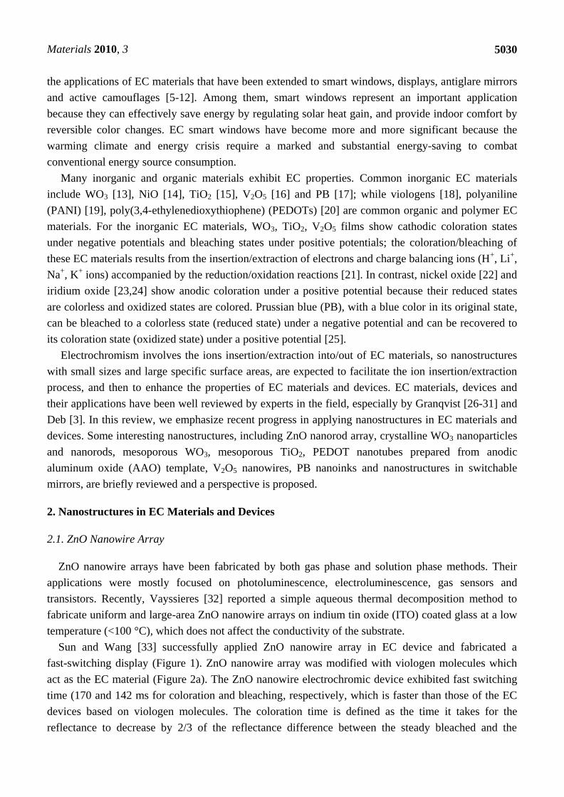
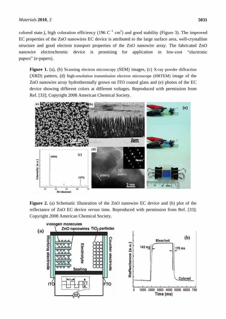
Sun and Wang [33] successfully applied ZnO nanowire array in EC device and fabricated a
fast-switching display (Figure 1). ZnO nanowire array was modified with viologen molecules which
act as the EC material (Figure 2a). The ZnO nanowire electrochromic device exhibited fast switching
time (170 and 142 ms for coloration and bleaching, respectively, which is faster than those of the EC
devices based on viologen molecules. The coloration time is defined as the time it takes for the
reflectance to decrease by 2/3 of the reflectance difference between the steady bleached and the
Materials 2010, 3
5031
colored state.), high coloration efficiency (196 C−1
cm2) and good stability (Figure 3). The improved
EC properties of the ZnO nanowires EC device is attributed to the large surface area, well-crystalline
structure and good electron transport properties of the ZnO nanowire array. The fabricated ZnO
nanowire electrochromic device is promising for application in low-cost ―electronic
papers‖ (e-papers).
Figure 1. (a), (b) Scanning electron microscopy (SEM) images, (c) X-ray powder diffraction
(XRD) pattern, (d) high-resolution transmission electron microscope (HRTEM) image of the
ZnO nanowire array hydrothermally grown on ITO coated glass and (e) photos of the EC
device showing different colors at different voltages. Reproduced with permission from
Ref. [33]; Copyright 2008 American Chemical Society.
Figure 2. (a) Schematic illustration of the ZnO nanowire EC device and (b) plot of the
reflectance of ZnO EC device versus time. Reproduced with permission from Ref. [33];
Copyright 2008 American Chemical Society.
(e)
(a)
Materials 2010, 3
5032
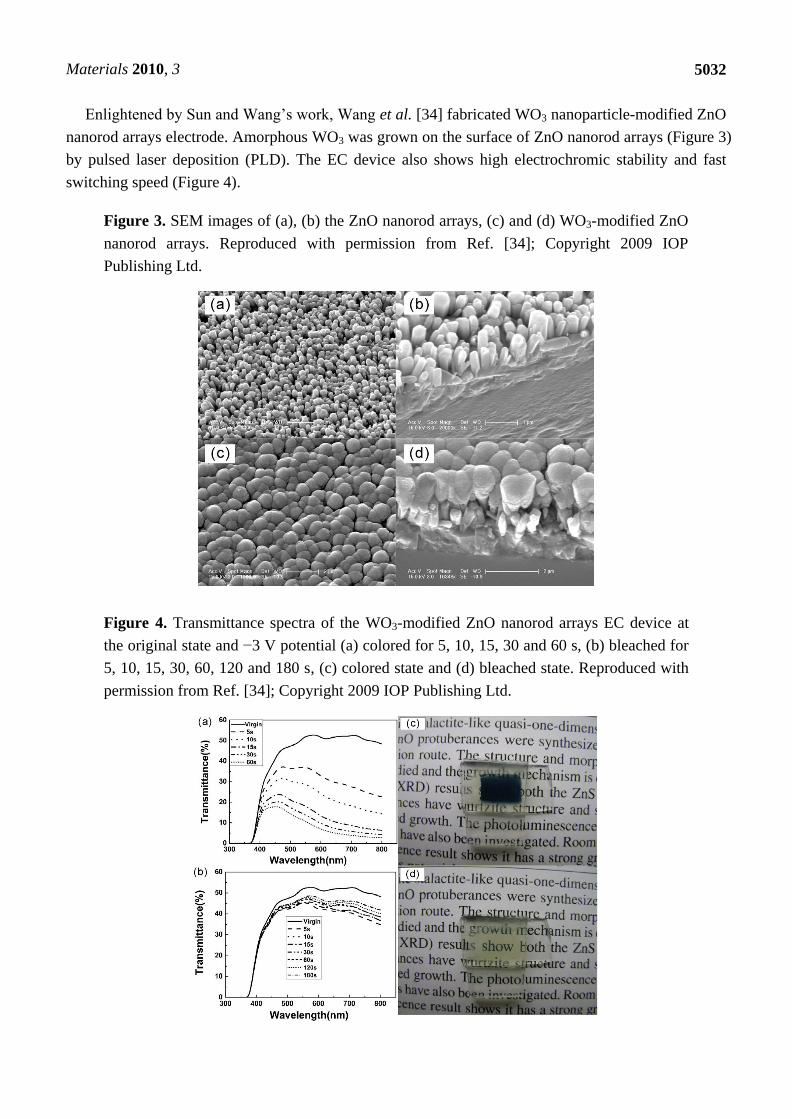
Enlightened by Sun and Wang’s work, Wang et al. [34] fabricated WO3 nanoparticle-modified ZnO
nanorod arrays electrode. Amorphous WO3 was grown on the surface of ZnO nanorod arrays (Figure 3)
by pulsed laser deposition (PLD). The EC device also shows high electrochromic stability and fast
switching speed (Figure 4).
Figure 3. SEM images of (a), (b) the ZnO nanorod arrays, (c) and (d) WO3-modified ZnO
nanorod arrays. Reproduced with permission from Ref. [34]; Copyright 2009 IOP
Publishing Ltd.
Figure 4. Transmittance spectra of the WO3-modified ZnO nanorod arrays EC device at
the original state and −3 V potential (a) colored for 5, 10, 15, 30 and 60 s, (b) bleached for
5, 10, 15, 30, 60, 120 and 180 s, (c) colored state and (d) bleached state. Reproduced with
permission from Ref. [34]; Copyright 2009 IOP Publishing Ltd.
Materials 2010, 3
5033
2.2. Crystalline WO3 Nanostructures
Most of the EC investigations on WO3 were focused on its amorphous films [35-37]. Compared
with the amorphous structure, crystalline WO3 is much more stable due to the denser structure and
slower dissolution rate in electrolytes. However, crystalline WO3 bulk material usually has slow
switching response. To improve the switching response, nanocrystalline WO3 were applied in EC
materials and devices in recent years.
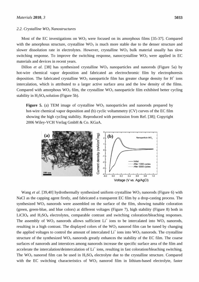
Dillon et al. [38] has synthesized crystalline WO3 nanoparticles and nanorods (Figure 5a) by
hot-wire chemical vapor deposition and fabricated an electrochromic film by electrophoresis
deposition. The fabricated crystalline WO3 nanoparticle film has greater charge density for H+ ions
intercalation, which is attributed to a larger active surface area and the low density of the films.
Compared with amorphous WO3 film, the crystalline WO3 nanoparticle film exhibited better cycling
stability in H2SO4 solution (Figure 5b).
Figure 5. (a) TEM image of crystalline WO3 nanoparticles and nanorods prepared by
hot-wire chemical vapor deposition and (b) cyclic voltammetry (CV) curves of the EC film
showing the high cycling stability. Reproduced with permission from Ref. [38]; Copyright
2006 Wiley-VCH Verlag GmbH & Co. KGaA.
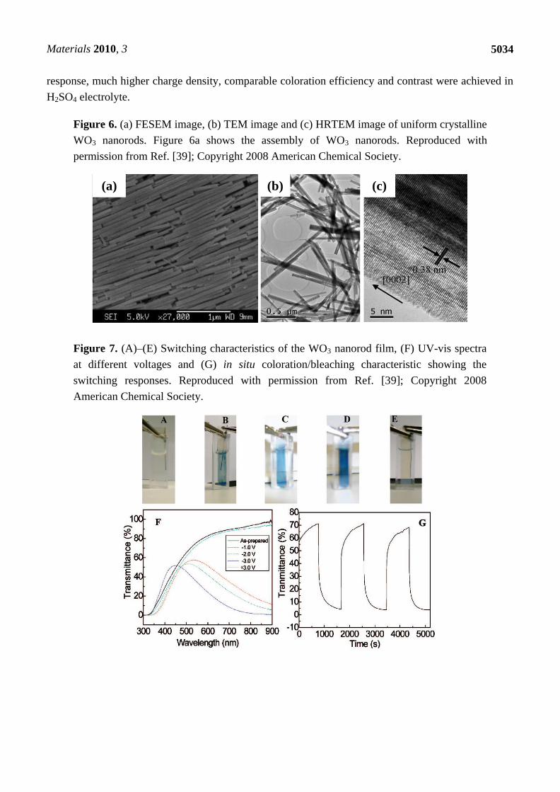
Wang et al. [39,40] hydrothermally synthesized uniform crystalline WO3 nanorods (Figure 6) with
NaCl as the capping agent firstly, and fabricated a transparent EC film by a drop-casting process. The
synthesized WO3 nanorods were assembled on the surface of the film, showing tunable coloration
(green, green-blue, and blue colors) at different voltages (Figure 7), high stability (Figure 8) both in
LiClO4 and H2SO4 electrolytes, comparable contrast and switching coloration/bleaching responses.
The assembly of WO3 nanorods allows sufficient Li+ ions to be intercalated into WO3 nanorods,
resulting in a high contrast. The displayed colors of the WO3 nanorod film can be tuned by changing
the applied voltages to control the amount of intercalated Li+ ions into WO3 nanorods. The crystalline
structure of the synthesized WO3 nanorods greatly enhances the stability of the EC film. The coarse
surfaces of nanorods and interstices among nanorods increase the specific surface area of the film and
accelerate the intercalation/deintercalation of Li+ ions, resulting in fast coloration/bleaching switching.
The WO3 nanorod film can be used in H2SO4 electrolyte due to the crystalline structure. Compared
with the EC switching characteristics of WO3 nanorod film in lithium-based electrolyte, faster
(a) (b)
Materials 2010, 3
5034
response, much higher charge density, comparable coloration efficiency and contrast were achieved in
H2SO4 electrolyte.
Figure 6. (a) FESEM image, (b) TEM image and (c) HRTEM image of uniform crystalline
WO3 nanorods. Figure 6a shows the assembly of WO3 nanorods. Reproduced with
permission from Ref. [39]; Copyright 2008 American Chemical Society.
Figure 7. (A)–(E) Switching characteristics of the WO3 nanorod film, (F) UV-vis spectra
at different voltages and (G) in situ coloration/bleaching characteristic showing the
switching responses. Reproduced with permission from Ref. [39]; Copyright 2008
American Chemical Society.
(a) (b) (c)
Materials 2010, 3
5035
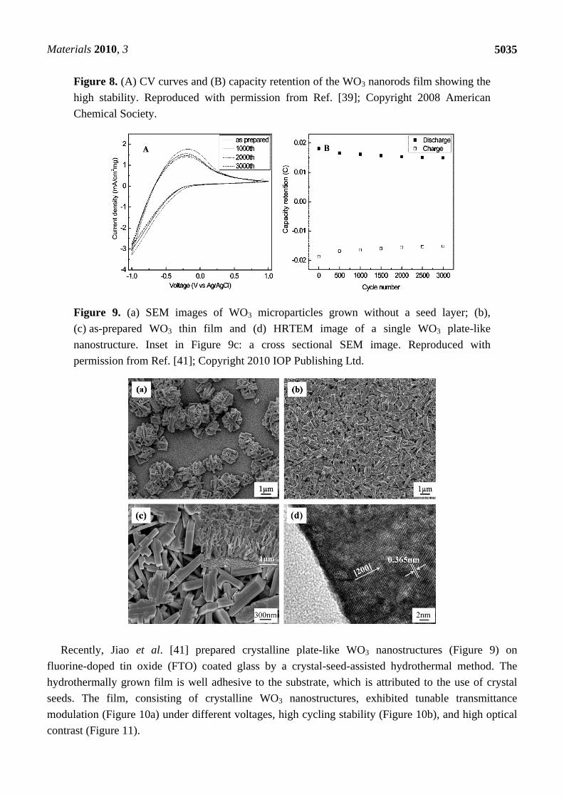
Figure 8. (A) CV curves and (B) capacity retention of the WO3 nanorods film showing the
high stability. Reproduced with permission from Ref. [39]; Copyright 2008 American
Chemical Society.
Figure 9. (a) SEM images of WO3 microparticles grown without a seed layer; (b),
(c) as-prepared WO3 thin film and (d) HRTEM image of a single WO3 plate-like
nanostructure. Inset in Figure 9c: a cross sectional SEM image. Reproduced with
permission from Ref. [41]; Copyright 2010 IOP Publishing Ltd.
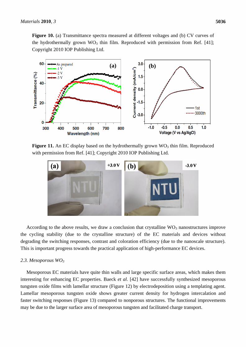
Recently, Jiao et al. [41] prepared crystalline plate-like WO3 nanostructures (Figure 9) on
fluorine-doped tin oxide (FTO) coated glass by a crystal-seed-assisted hydrothermal method. The
hydrothermally grown film is well adhesive to the substrate, which is attributed to the use of crystal
seeds. The film, consisting of crystalline WO3 nanostructures, exhibited tunable transmittance
modulation (Figure 10a) under different voltages, high cycling stability (Figure 10b), and high optical
contrast (Figure 11).
Materials 2010, 3
5036
Figure 10. (a) Transmittance spectra measured at different voltages and (b) CV curves of
the hydrothermally grown WO3 thin film. Reproduced with permission from Ref. [41];
Copyright 2010 IOP Publishing Ltd.
Figure 11. An EC display based on the hydrothermally grown WO3 thin film. Reproduced
with permission from Ref. [41]; Copyright 2010 IOP Publishing Ltd.
According to the above results, we draw a conclusion that crystalline WO3 nanostructures improve
the cycling stability (due to the crystalline structure) of the EC materials and devices without
degrading the switching responses, contrast and coloration efficiency (due to the nanoscale structure).
This is important progress towards the practical application of high-performance EC devices.
2.3. Mesoporous WO3
Mesoporous EC materials have quite thin walls and large specific surface areas, which makes them
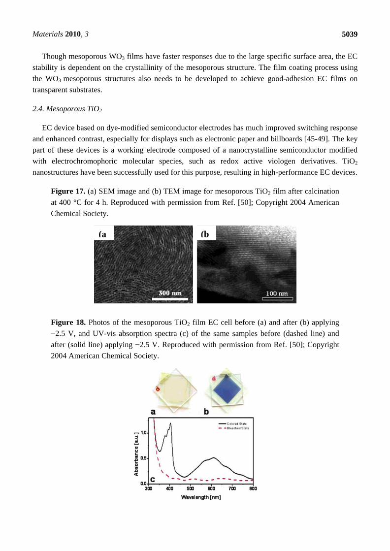
interesting for enhancing EC properties. Baeck et al. [42] have successfully synthesized mesoporous
tungsten oxide films with lamellar structure (Figure 12) by electrodeposition using a templating agent.
Lamellar mesoporous tungsten oxide shows greater current density for hydrogen intercalation and
faster switching responses (Figure 13) compared to nonporous structures. The functional improvements
may be due to the larger surface area of mesoporous tungsten and facilitated charge transport.
(a) (b)
Materials 2010, 3
5037
Figure 12. TEM images of tungsten oxide films (a) deposited at −0.2 V, yielding a
wormhole-like structure, (b) deposited at −0.5 V, resulting in a lamellar structure.
Reproduced with permission from Ref. [42]; Copyright 2003 Wiley-VCH Verlag GmbH &
Co. KGaA.
Figure 13. Chronoamperometry with voltage step from −0.5 to + 0.5 V (solid line: lamellar
phase mesoporous tungsten oxide, dashed line: control film). Reproduced with permission
from Ref. [42]; Copyright 2003 Wiley-VCH Verlag GmbH & Co. KGaA.
Brezesinski et al. [43] synthesized mesoporous WO3 EC thin film (Figure 14) by
evaporation-induced self-assembly using a block-copolymer template. The three-dimensional
mesoporosity significantly improves the electrochromic response times, because of shorter diffusion
pathlengths compared to the dense materials (Figure 15). The combination of mesoporosity and
crystallinity leads to improved reversibility of ion insertion/extraction and cycling stability.
Amorphous mesoporous WO3 films suffer from irreversible degradation because of their structural
modifications. By annealing at 550 °C in air, fully crystalline mesoporous WO3 thin films are obtained.
Sallard et al. [44] also prepared crystalline mesoporous WO3 films (Figure 16) by annealing
amorphous mesoporous WO3 films. The crystallinity degree ranging from fully amorphous to
crystalline can be adjusted without mesostructural collapse. Electrochemical results show that only the
highly crystalline mesoporous WO3 films exhibit long-term EC stability.

Materials 2010, 3
5038
Figure 14. (a) TEM image, (b) Selected area electron diffraction (SAED) pattern and
(c) HRTEM image of the mesoporous ordered WO3 network after crystallization.
(d) Fourier transform of the image shown in (c). Reproduced with permission, Ref. [43];
Copyright 2006 Wiley-VCH Verlag GmbH & Co. KGaA.
Figure 15. Coloration-bleaching characteristics of mesoporous WO3 films at a wavelength
of 630 nm and at voltage steps of ±1 V. Reproduced with permission from Ref. [43];
Copyright 2006 Wiley-VCH Verlag GmbH & Co. KGaA.
Figure 16. (a), (b) TEM images and (c) tapping mode AFM images of periodically ordered
WO3 thin films after crystallization at 550 °C showing the homogeneity of the mesoporous
structure. Reproduced with permission from Ref. [44]; Copyright 2007 American
Chemical Society.
Materials 2010, 3
5039
Though mesoporous WO3 films have faster responses due to the large specific surface area, the EC
stability is dependent on the crystallinity of the mesoporous structure. The film coating process using
the WO3 mesoporous structures also needs to be developed to achieve good-adhesion EC films on
transparent substrates.
2.4. Mesoporous TiO2
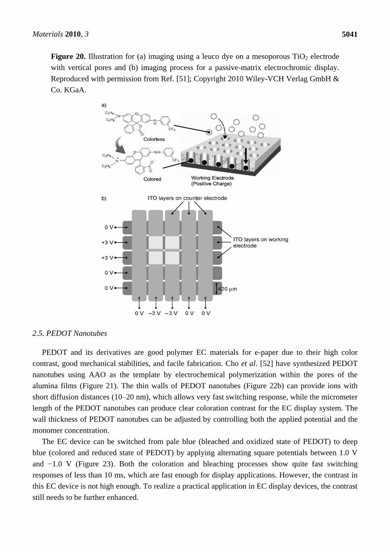
EC device based on dye-modified semiconductor electrodes has much improved switching response
and enhanced contrast, especially for displays such as electronic paper and billboards [45-49]. The key
part of these devices is a working electrode composed of a nanocrystalline semiconductor modified
with electrochromophoric molecular species, such as redox active viologen derivatives. TiO2
nanostructures have been successfully used for this purpose, resulting in high-performance EC devices.
Figure 17. (a) SEM image and (b) TEM image for mesoporous TiO2 film after calcination
at 400 °C for 4 h. Reproduced with permission from Ref. [50]; Copyright 2004 American
Chemical Society.
Figure 18. Photos of the mesoporous TiO2 film EC cell before (a) and after (b) applying
−2.5 V, and UV-vis absorption spectra (c) of the same samples before (dashed line) and
after (solid line) applying −2.5 V. Reproduced with permission from Ref. [50]; Copyright
2004 American Chemical Society.
(a
)
(b
)

Materials 2010, 3
5040
Figure 19. (a) Transient absorbance at 608 nm of the electrochromic cell made of
viologen-modified mesoporous TiO2 and nanoscrystalline TiO2 electrodes following
application of −2.5 V and 2.5 V, (b) relative absorbance profile of the colored state and
bleached state of the electrochromic cells. Reproduced with permission from Ref. [50];
Copyright 2004 American Chemical Society.
Choi et al. [50] synthesized viologen modified mesoporous TiO2 film (Figure 17) with hexagonally
close-packed mesopores and channel walls made of 8–10 nm anatase nanostructures. The film
exhibited similar switching speed and reversibility as nanocrystalline titania but better contrast
(Figure 18 and 19). The higher contrast can be attributed to a contiguous pathway of well-connected
anatase nanocrystallites arranged into a well-defined mesoporous architecture, which results in a
greater volume density of loaded viologen molecules.
Weng et al. [51] demonstrated a high-speed passive-matrix EC display using a leuco modified
mesoporous TiO2 electrode with vertical porosity (Figure 20). The device exhibited better background
whiteness, which improves readability and reduces eyestrain. Imaging and erasing can be carried out
by applying a potential of ±3.0 V. The thickness of the mesoporous layer critically affects the contrast
of the displayed image. Upon writing, the clear images can remain for a few minutes without
becoming blurry because the vertical pores of the electrode can support effective diffusion of leuco
dyes perpendicular to the electrode and prevent the diffusion of the dye around the electrode. The
leuco modified mesoporous TiO2 electrode shows potential for the realization of a full-color reflective
display for use in e-papers.
Materials 2010, 3
5041
Figure 20. Illustration for (a) imaging using a leuco dye on a mesoporous TiO2 electrode
with vertical pores and (b) imaging process for a passive-matrix electrochromic display.
Reproduced with permission from Ref. [51]; Copyright 2010 Wiley-VCH Verlag GmbH &
Co. KGaA.
2.5. PEDOT Nanotubes
PEDOT and its derivatives are good polymer EC materials for e-paper due to their high color
contrast, good mechanical stabilities, and facile fabrication. Cho et al. [52] have synthesized PEDOT
nanotubes using AAO as the template by electrochemical polymerization within the pores of the
alumina films (Figure 21). The thin walls of PEDOT nanotubes (Figure 22b) can provide ions with
short diffusion distances (10–20 nm), which allows very fast switching response, while the micrometer
length of the PEDOT nanotubes can produce clear coloration contrast for the EC display system. The
wall thickness of PEDOT nanotubes can be adjusted by controlling both the applied potential and the
monomer concentration.
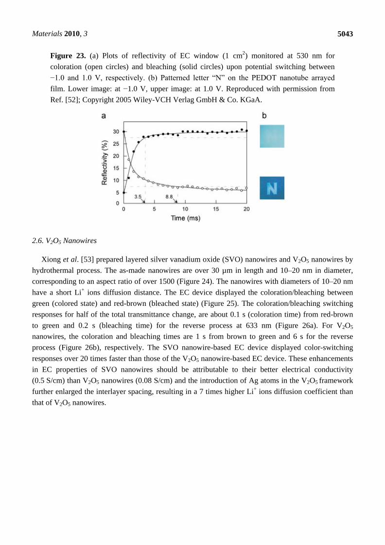
The EC device can be switched from pale blue (bleached and oxidized state of PEDOT) to deep
blue (colored and reduced state of PEDOT) by applying alternating square potentials between 1.0 V
and −1.0 V (Figure 23). Both the coloration and bleaching processes show quite fast switching
responses of less than 10 ms, which are fast enough for display applications. However, the contrast in
this EC device is not high enough. To realize a practical application in EC display devices, the contrast
still needs to be further enhanced.
Materials 2010, 3
5042
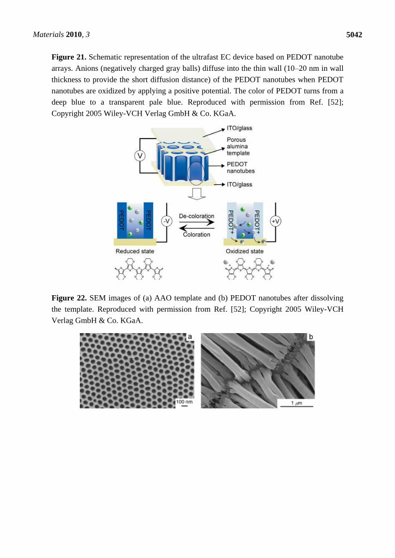
Figure 21. Schematic representation of the ultrafast EC device based on PEDOT nanotube
arrays. Anions (negatively charged gray balls) diffuse into the thin wall (10–20 nm in wall
thickness to provide the short diffusion distance) of the PEDOT nanotubes when PEDOT
nanotubes are oxidized by applying a positive potential. The color of PEDOT turns from a
deep blue to a transparent pale blue. Reproduced with permission from Ref. [52];
Copyright 2005 Wiley-VCH Verlag GmbH & Co. KGaA.
Figure 22. SEM images of (a) AAO template and (b) PEDOT nanotubes after dissolving
the template. Reproduced with permission from Ref. [52]; Copyright 2005 Wiley-VCH
Verlag GmbH & Co. KGaA.
Materials 2010, 3
5043
Figure 23. (a) Plots of reflectivity of EC window (1 cm2) monitored at 530 nm for
coloration (open circles) and bleaching (solid circles) upon potential switching between
−1.0 and 1.0 V, respectively. (b) Patterned letter ―N‖ on the PEDOT nanotube arrayed
film. Lower image: at −1.0 V, upper image: at 1.0 V. Reproduced with permission from
Ref. [52]; Copyright 2005 Wiley-VCH Verlag GmbH & Co. KGaA.
2.6. V2O5 Nanowires
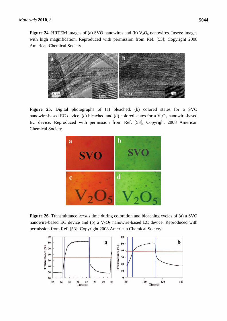
Xiong et al. [53] prepared layered silver vanadium oxide (SVO) nanowires and V2O5 nanowires by
hydrothermal process. The as-made nanowires are over 30 µm in length and 10–20 nm in diameter,
corresponding to an aspect ratio of over 1500 (Figure 24). The nanowires with diameters of 10–20 nm
have a short Li+ ions diffusion distance. The EC device displayed the coloration/bleaching between
green (colored state) and red-brown (bleached state) (Figure 25). The coloration/bleaching switching
responses for half of the total transmittance change, are about 0.1 s (coloration time) from red-brown
to green and 0.2 s (bleaching time) for the reverse process at 633 nm (Figure 26a). For V2O5
nanowires, the coloration and bleaching times are 1 s from brown to green and 6 s for the reverse
process (Figure 26b), respectively. The SVO nanowire-based EC device displayed color-switching
responses over 20 times faster than those of the V2O5 nanowire-based EC device. These enhancements
in EC properties of SVO nanowires should be attributable to their better electrical conductivity
(0.5 S/cm) than V2O5 nanowires (0.08 S/cm) and the introduction of Ag atoms in the V2O5 framework
further enlarged the interlayer spacing, resulting in a 7 times higher Li+ ions diffusion coefficient than
that of V2O5 nanowires.
Materials 2010, 3
5044
Figure 24. HRTEM images of (a) SVO nanowires and (b) V2O5 nanowires. Insets: images
with high magnification. Reproduced with permission from Ref. [53]; Copyright 2008
American Chemical Society.
Figure 25. Digital photographs of (a) bleached, (b) colored states for a SVO
nanowire-based EC device, (c) bleached and (d) colored states for a V2O5 nanowire-based
EC device. Reproduced with permission from Ref. [53]; Copyright 2008 American
Chemical Society.
Figure 26. Transmittance versus time during coloration and bleaching cycles of (a) a SVO
nanowire-based EC device and (b) a V2O5 nanowire-based EC device. Reproduced with
permission from Ref. [53]; Copyright 2008 American Chemical Society.
Materials 2010, 3
5045
2.7. PB Nanoinks
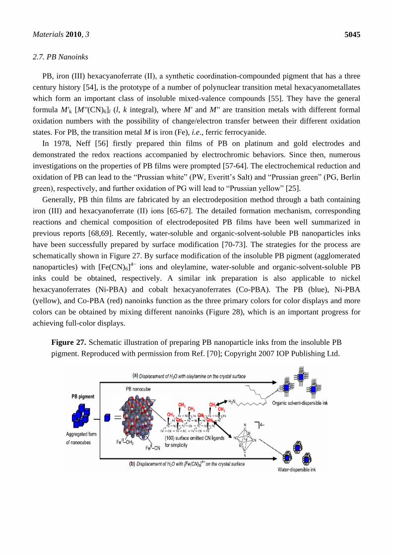
PB, iron (III) hexacyanoferrate (ІІ), a synthetic coordination-compounded pigment that has a three
century history [54], is the prototype of a number of polynuclear transition metal hexacyanometallates
which form an important class of insoluble mixed-valence compounds [55]. They have the general
formula M'k [M''(CN)6]l (l, k integral), where M' and M'' are transition metals with different formal
oxidation numbers with the possibility of change/electron transfer between their different oxidation
states. For PB, the transition metal M is iron (Fe), i.e., ferric ferrocyanide.
In 1978, Neff [56] firstly prepared thin films of PB on platinum and gold electrodes and
demonstrated the redox reactions accompanied by electrochromic behaviors. Since then, numerous
investigations on the properties of PB films were prompted [57-64]. The electrochemical reduction and
oxidation of PB can lead to the ―Prussian white‖ (PW, Everitt’s Salt) and ―Prussian green‖ (PG, Berlin
green), respectively, and further oxidation of PG will lead to ―Prussian yellow‖ [25].
Generally, PB thin films are fabricated by an electrodeposition method through a bath containing
iron (III) and hexacyanoferrate (ІІ) ions [65-67]. The detailed formation mechanism, corresponding
reactions and chemical composition of electrodeposited PB films have been well summarized in
previous reports [68,69]. Recently, water-soluble and organic-solvent-soluble PB nanoparticles inks
have been successfully prepared by surface modification [70-73]. The strategies for the process are
schematically shown in Figure 27. By surface modification of the insoluble PB pigment (agglomerated
nanoparticles) with [Fe(CN)6]4−
ions and oleylamine, water-soluble and organic-solvent-soluble PB
inks could be obtained, respectively. A similar ink preparation is also applicable to nickel
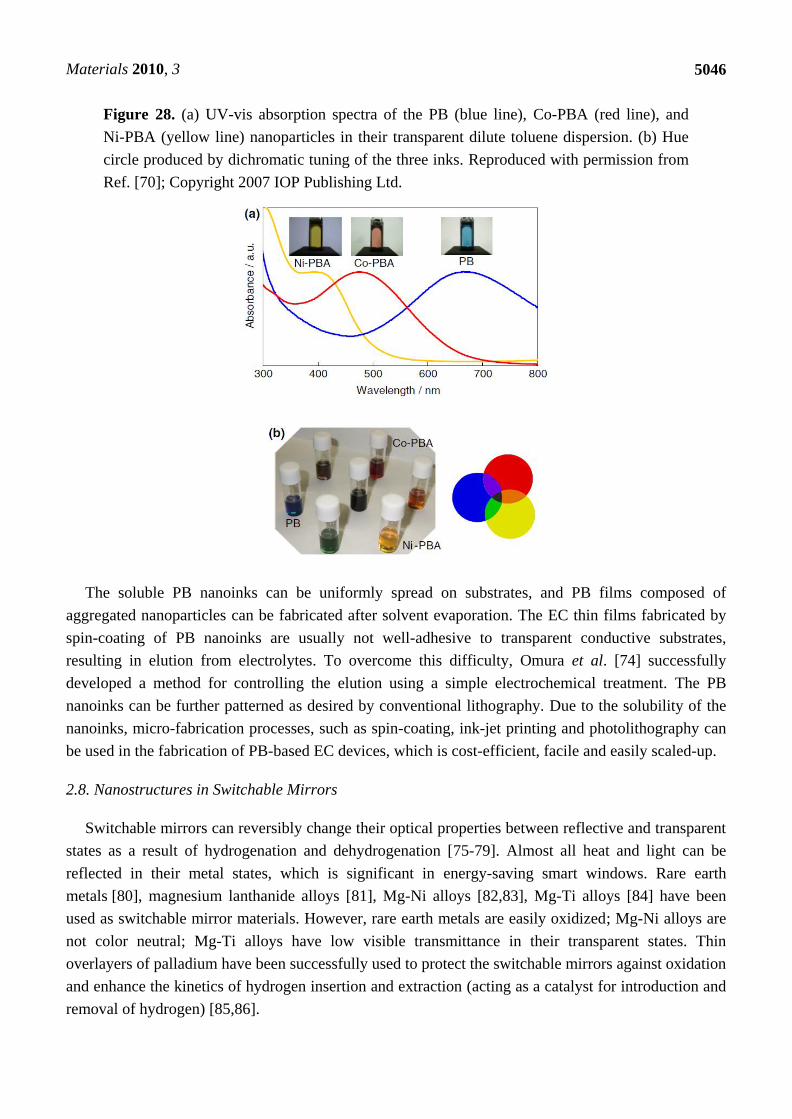
hexacyanoferrates (Ni-PBA) and cobalt hexacyanoferrates (Co-PBA). The PB (blue), Ni-PBA
(yellow), and Co-PBA (red) nanoinks function as the three primary colors for color displays and more
colors can be obtained by mixing different nanoinks (Figure 28), which is an important progress for
achieving full-color displays.
Figure 27. Schematic illustration of preparing PB nanoparticle inks from the insoluble PB
pigment. Reproduced with permission from Ref. [70]; Copyright 2007 IOP Publishing Ltd.
Materials 2010, 3
5046
Figure 28. (a) UV-vis absorption spectra of the PB (blue line), Co-PBA (red line), and
Ni-PBA (yellow line) nanoparticles in their transparent dilute toluene dispersion. (b) Hue
circle produced by dichromatic tuning of the three inks. Reproduced with permission from
Ref. [70]; Copyright 2007 IOP Publishing Ltd.
The soluble PB nanoinks can be uniformly spread on substrates, and PB films composed of
aggregated nanoparticles can be fabricated after solvent evaporation. The EC thin films fabricated by
spin-coating of PB nanoinks are usually not well-adhesive to transparent conductive substrates,
resulting in elution from electrolytes. To overcome this difficulty, Omura et al. [74] successfully
developed a method for controlling the elution using a simple electrochemical treatment. The PB
nanoinks can be further patterned as desired by conventional lithography. Due to the solubility of the
nanoinks, micro-fabrication processes, such as spin-coating, ink-jet printing and photolithography can
be used in the fabrication of PB-based EC devices, which is cost-efficient, facile and easily scaled-up.
2.8. Nanostructures in Switchable Mirrors
Switchable mirrors can reversibly change their optical properties between reflective and transparent
states as a result of hydrogenation and dehydrogenation [75-79]. Almost all heat and light can be
reflected in their metal states, which is significant in energy-saving smart windows. Rare earth
metals [80], magnesium lanthanide alloys [81], Mg-Ni alloys [82,83], Mg-Ti alloys [84] have been
used as switchable mirror materials. However, rare earth metals are easily oxidized; Mg-Ni alloys are
not color neutral; Mg-Ti alloys have low visible transmittance in their transparent states. Thin
overlayers of palladium have been successfully used to protect the switchable mirrors against oxidation
and enhance the kinetics of hydrogen insertion and extraction (acting as a catalyst for introduction and
removal of hydrogen) [85,86].
Materials 2010, 3
5047
Recently, Yamada et al. prepared switchable mirrors based on Mg-Ca alloy thin films by magnetron
sputtering [87]. The switchable mirrors looked completely color neutral with high visible transmittance
in the transparent state, which may be attributed to the grayish neutral hydrogenated state of MgH2
and MgCaH3.72.
Metallic copper exhibits very high near-infrared reflectance and much less reflectance below
~600 nm; Cu2O has low reflectance in both the visible and near-IR spectra. Metallic thin films of
antimony and bismuth, deposited on glass substrates by vacuum evaporation, can be reversibly
converted to transparent, semiconducting lithium pnictides by cathodic polarization in a nonaqueous
lithium electrolyte. These characteristics make copper-copper (I) oxide, Sb-Li, Bi-Li [88] and
Sb-Cu-Li [89] attractive in switchable mirrors.
3. Conclusions and Perspective
Since the discovery of EC materials, extensive investigations have been carried out to improve their
EC properties, including enhancement of the switching responses; contrast; coloration efficiency and
cycling stability; as well as EC device fabrications and applications. ZnO nanowire/nanorod arrays
modified by EC materials, mesoporous and tubular EC materials significantly enhance the switching
responses of EC devices, for potential application in fast-switching displays and e-papers. Crystalline
WO3 nanoparticles, nanorods and crystalline mesoporous WO3 exhibit enhanced EC stability and
contrast, especially in acidic electrolytes. Soluble PB and its analogues Ni-PBA, Co-PBA nanoinks
exhibit blue, yellow and red colors, promising the possibility of achieving full-color displays. Due to
the solubility of the nanoinks, micro-fabrication processes, such as spin-coating, ink-jet printing and
photolithography, can be used in the fabrication of PB-based EC devices, which is cost-efficient, facile
and easily scaled-up. Switchable mirrors are the most effective energy-saving EC devices in all kinds
of smart windows. However, the metal alloys are easily oxidized, resulting in a poor
long-term stability.
Further efforts are needed to accelerate practical applications of EC devices. For large-area EC
devices, the difficulties may be in slow responses, poor stability and high cost. To overcome these
difficulties, the synthesis of new nanostructured EC materials needs to be developed. The ideal
nanostructures for EC materials may include ultrathin crystalline nanorods, nanowires or nanotubes,
crystalline mesoporous structures and quantum dots. These nanostructures with large specific surface
areas, are expected to possess fast and stable EC switching. Low-cost synthesis routes for these EC
nanostructures are favorable. The coating process for EC nanostructures also needs to develop to
obtain well-adhesive EC films on transparent conductive substrates. The combination of different
kinds of EC materials is also worthwhile, for example, to exhibit multi-colors and to enhance the
coloration modulation and stability. Complimentary EC devices need further development to enhance
the contrast, coloration efficiency and stability of EC devices. Inorganic-organic hybrid EC devices are
also promising for practical application, for example in e-papers. Besides the developments of EC
materials and devices, transparent conductive substrates with better conductivity, solid-state
electrolytes, advanced sealing and packaging technologies, are also critical and deserve intensive
investigations for the practical applications of EC materials and devices. Gallium doped ZnO (GZO),
antimony doped tin oxide (ATO), carbon nanotubes or graphene coated glass are promising substitutes
Materials 2010, 3
5048
to replace ITO. Low-cost processes for the fabrication of EC devices must be developed to realize their
practical applications, which need the cooperation of researchers and technicians to solve both
scientific and technical challenges.
Acknowledgements
The authors thank the invitation of Claes-Göran Granqvist for this review. Financial support from the
National Science Foundation of China (Project Number 61076015) is gratefully acknowledged.
References
1. Granqvist, C.G. Handbook of Inorganic Electrochromic Materials; Elsevier: Amsterdam, The
Netherlands, 1995.
2. Deb, S.K. Reminiscences on the discovery of electrochromic phenomena in transition metal
oxides. Solar Energ. Mater. Solar Cells 1995, 39, 191-201.
3. Deb, S.K. Opportunities and challenges in science and technology of WO3 for electrochromic and
related applications. Solar Energ. Mater. Solar Cells 2008, 92, 245-258.
4. Deb, S.K. A novel electrophotographic system. Appl. Opt. Suppl. 1969, 3, 192-195.
5. Deb, S.K. Optical and photoelectric properties and color centres in thin films of tungsten oxide.
Philos. Mag. 1973, 27, 801-822.
6. Campus, F.; Bonhôte, P.; Grätzel, M.; Heinen S.; Walder, L. Electrochromic devices based on
surface-modified nanocrystalline TiO2 thin-film electrodes. Solar Energ. Mater. Solar Cells 1999,
56, 281-297.
7. Shim, G.H.; Han, M.G; Sharp-Norton, J.C.; Creagerb, S.E.; Foulger, S.H. Inkjet-printed
electrochromic devices utilizing polyaniline-silica and poly(3,4-ethylenedioxythiophene)-silica
colloidal composite particles. J. Mater. Chem. 2008, 18, 594-601.
8. Liao, C.-C.; Chen, F.-R.; Kai, J.-J. Electrochromic properties of nanocomposite WO3 films. Solar
Energ. Mater. Solar Cells 2007, 91, 1282-1288.
9. Mortimer, R.J.; Dyer, A.L.; Reynolds, J.R. Electrochromic organic and polymeric materials for
display applications. Displays 2006, 27, 2-18.
10. Granqvist, C.G.; Azensa, A.; Hjelm, A.; Kullman, L.; Niklasson, G.A.; Rönnow, D.; Mattsson,
M.S.; Veszelei, M.; Vaivars, G. Recent advances in electrochromics for smart windows
applications. Solar Energ. 1998, 63, 199-216.
11. Granqvist, C.G. Electrochromic tungsten oxide films: Review of progress 1993-1998. Solar Energ.
Mater. Solar Cells 2000, 60, 201-262.
12. Baetens, R.; Jelle, B.P.; Gustavsen, A. Properties, requirements and possibilities of smart
windows for dynamic daylight and solar energy control in buildings: A state-of-the-art review.
Solar Energ. Mater. Solar Cells 2010, 94, 87-105.
13. Yoo, S.J.; Lim, J.W.; Sung, Y.-E.; Jung, Y.H.; Choi, H.G.; Kim, D.K. Fast switchable
electrochromic properties of tungsten oxide nanowire bundles. Appl. Phys. Lett. 2007, 90, 173126.
14. Wu, M.-S.; Yang, C.-H. Electrochromic properties of intercrossing nickel oxide nanoflakes
synthesized by electrochemically anodic deposition. Appl. Phys. Lett. 2007, 91, 033109.
Materials 2010, 3
5049
15. Ghicov, A.; Albu, S.P.; Macak, J.M.; Schmuki, P. High-contrast electrochromic switching using
transparent lift-off layers of self-organized TiO2 nanotubes. Small 2008, 4, 1063-1066.
16. Cheng, K.-C.; Chen, F.-R.; Kai, J.-J. V2O5 nanowires as a functional material for electrochromic
device. Solar Energ. Mater. Solar Cells 2006, 90, 1156-1165.
17. Cheng, K.-C.; Chen, F.-R.; Kai, J.-J. Electrochromic property of nano-composite Prussian blue
based thin film. Electrochim. Acta 2007, 52, 3330-3335.
18. Cinnsealach, R.; Boschloo, G.; Rao, S.N.; Fitzmaurice, D. Electrochromic windows based on
viologen-modified nanostructured TiO2 films. Solar Energ. Mater. Solar Cells 1998, 55, 215-223.
19. Gospodinova, N.; Terlemezyan, L. Conducting polymers prepared by oxidative polymerization:
polyaniline. Prog. Polym. Sci. 1998, 23, 1443-1484.
20. Andersson, P.; Forchheimer, R.; Tehrani, P.; Berggren, M. Printable all-organic electrochromic
active-matrix displays. Adv. Funct. Mater. 2007, 17, 3074-3082.
21. Niklasson, G.A.; Granqvist, C.G. Electrochromics for smart windows: thin films of tungsten oxide
and nickel oxide, and devices based on these. J. Mater. Chem. 2007, 17, 127-156.
22. Avendaño, E.; Berggren, L.; Niklasson, G.A.; Granqvist, C.G.; Azens, A. Electrochromic
materials and devices: Brief survey and new data on optical absorption in tungsten oxide and
nickel oxide films. Thin Solid Films 2006, 496, 30-36.
23. Dautremont-Smith, W.C.; Beni, G.; Schiavone, L.M.; Shay, J.L. Solid-state electrochromic cell
with anodic iridium oxide film electrodes. Appl. Phys. Lett. 1979, 35, 565.
24. Patila, P.S.; Kawarb, R.K.; Sadale, S.B. Electrochromism in spray deposited iridium oxide thin
films. Electrochim. Acta 2005, 50, 2527-2532.
25. DeLongchamp, D.M.; Hammond, P.T. High-contrast electrochromism and controllable
dissolution of assembled Prussian blue/polymer nanocomposites. Adv. Funct. Mater. 2004, 14,
224-232.
26. Granqvist, C.G. Solar energy materials. Adv. Mater. 2003, 15, 1789-1803.
27. Granqvist, C.G.; Avendaño, E.; Azens, A. Electrochromic coatings and devices: survey of some
recent advances. Thin Solid Films 2003, 442, 201-211.
28. Granqvist, C.G.; Azens, A.; Heszler, P.; Kish, L.B.; Osterlund, L. Nanomaterials for benign
indoor environments: Electrochromics for ―smart windows‖, sensors for air quality, and
photo-catalysts for air cleaning. Solar Energ. Mater. Solar Cells 2007, 91, 355-365.
29. Granqvist, C.G. Oxide electrochromics: Why, how, and whither. Solar Energ. Mater. Solar Cells
2008, 92, 203-208.
30. Granqvist, C.G.; Lansaker, P.C.; Mlyuka, N.R.; Niklasson, G.A.; Avendaño, E. Progress in
chromogenics: New results for electrochromic and thermochromic materials and devices. Solar
Energ. Mater. Solar Cells 2009, 93, 2032-2039.
31. Granqvist, C.G.; Green, S.; Niklasson, G.A.; Mlyuka, N.R.; von Kræmer, S.; Georén, P. Advances
in chromogenic materials and devices. Thin Solid Films 2010, 518, 3046-3053.
32. Vayssieres, L. Growth of arrayed nanorods and nanowires of ZnO from aqueous solutions. Adv.
Mater. 2003, 15, 464-466.
33. Sun, X.W.; Wang, J.X. Fast switching electrochromic display using a viologen-modified ZnO
nanowire array electrode. Nano Lett. 2008, 8, 1884-1889.
Materials 2010, 3
5050
34. Wang M.J.; Fang G.J.; Yuan, L.Y.; Huang, H.H.; Sun, Z.H.; Liu, N.S.; Xia, S.H.; Zhao, X.Z.
High optical switching speed and flexible electrochromic display based on WO3 nanoparticles
with ZnO nanorod arrays’ supported electrode. Nanotechnology 2009, 20, 185304.
35. Deepa, M.; Joshi, A.G.; Srivastava, A.K.; Shivaprasad, S.M.; Agnihotry, S.A. Electrochromic
nanostructured tungsten oxide films by sol-gel: Structure and intercalation properties.
J. Electrochem. Soc. 2006, 153, C365-C376.
36. Deepa, M.; Saxena, T.K.; Singh, D.P.; Sood, K.N.; Agnihotry, S.A. Spin coated versus dip coated
electrochromic tungsten oxide films: Structure, morphology, optical and electrochemical
properties. Electrochim. Acta 2006, 51, 1974-1989.
37. Subrahmanyam, A.; Karuppasamy, A. Optical and electrochromic properties of oxygen sputtered
tungsten oxide (WO3) thin films. Solar Energ. Mater. Solar Cells 2007, 91, 266-274.
38. Lee, S.-H.; Deshpande, R.; Parilla, P.A.; Jones, K.M.; To, B.; Mahan, A.H.; Dillon, A.C.
Crystalline WO3 nanoparticles for highly improved electrochromic applications. Adv. Mater.
2006, 18, 763-766.
39. Wang, J.M.; Khoo, E.; Lee, P.S.; Ma, J. Synthesis, assembly and electrochromic properties of
uniform crystalline WO3 nanorods. J. Phys. Chem. C 2008, 112, 14306-14312.
40. Wang, J.M.; Khoo, E.; Lee, P.S.; Ma, J. Controlled synthesis of WO3 nanorods and their
electrochromic properties in H2SO4 electrolyte. J. Phys. Chem. C 2009, 113, 9655-9658.
41. Jiao, Z.H.; Sun, X.W.; Wang, J.M.; Ke, L.; Demir, H.V. Hydrothermally grown nanostructured
WO3 films and their electrochromic characteristics. J. Phys. D: Appl. Phys. 2010, 43, 285501.
42. Baeck, S.-H.; Choi, K.-S.; Jaramillo, T.E.; Stucky, G.D.; McFarland, E.W. Enhancement of
photocatalytic and electrochromic properties of electrochemically fabricated mesoporous WO3
thin films. Adv. Mater. 2003, 15, 1269-1273.
43. Brezesinski, T.; Fattakhova-Rohlfing, D.; Sallard, S.; Antonietti, M.; Smarsly, B.M. Highly
crystalline WO3 thin films with ordered 3D mesoporosity and improved electrochromic
performance. Small 2006, 10, 1203-1211.
44. Sallard, S.; Brezesinski, T.; Smarsly, B.M. Electrochromic stability of WO3 thin films with
nanometer-scale periodicity and varying degrees of crystallinity. J. Phys. Chem. C 2007, 111,
7200-7206.
45. Cinnsealach, R.; Boschloo, G.; Nagaraja, R.S.; Fitzmaurice, D. Solar Energ. Mater. Solar Cells
1999, 57, 107-125.
46. Bonhote, P.; Gogniat, E.; Gratzel, M.; Ashrit, P.V. Novel electrochromic devices based on
complementary nanocrystalline TiO2 and WO3 thin films. Thin Solid Films 1999, 350, 269-275.
47. Campus, F.; Bonhote, P.; Gratzel, M.; Heinen, S.; Walder, L. Electrochromic devices based on
surface-modified nanocrystalline TiO2 thin-film electrodes. Solar Energ. Mater. Solar Cells 1999,
56, 281-297.
48. Cummins, D.; Boschloo, G.; Ryan, M.; Corr, D.; Nagaraja, R.S.; Fitzmaurice, D. Ultrafast
electrochromic windows based on redox-chromophore modified nanostructured semiconducting
and conducting films. J. Phys. Chem. B 2000, 104, 11449-11459.
49. Bach, U.; Corr, D.; Lupo, D.; Pichot, F.; Ryan, M. Nanomaterials-based electrochromics for
paper-quality displays. Adv. Mater. 2002, 14, 845-848.
Materials 2010, 3
5051
50. Choi, S.Y.; Mamak, M.; Coombs, N.; Chopra, N.; Ozin, G.A. Electrochromic performance of
viologen-modified periodic mesoporous nanocrystalline anatase electrodes. Nano Lett. 2004, 4,
1231-1235.
51. Weng, W.; Higuchi, T.; Suzuki, M.; Fukuoka, T.; Shimomura, T.; Ono, M.; Radhakrishnan, L.;
Wang, H.; Suzuki, N.; Hamid O.; Yamauchi, Y. A high-speed passive-matrix electrochromic
display using a mesoporous TiO2 electrode with vertical porosity. Angew. Chem. Int. Ed. 2010, 49,
3956-3959.
52. Cho, C.I.; Kwon, W.J.; Choi, S.-J.; Kim, P.; Park, S.-A.; Kim, J.; Son, S.J.; Xiao, R.; Kim, S.-H.;
Lee, S.B. Nanotube-based ultrafast electrochromic display. Adv. Mater. 2005, 17, 171-175.
53. Xiong, C.; Aliev, A.E.; Gnade, B.; Balkus, K.J., Jr. Fabrication of silver vanadium oxide and
V2O5 nanowires for electrochromics. ACS Nano 2008, 2, 293-301.
54. Brown, J. Observations and experiments upon the foregoing preparation. Philos. Trans. 1724, 33,
17-24.
55. Sharpe, A.G. The Chemistry of Cysno Complexes of the Transition Metals; Academic Press: New
York, NY, USA, 1976.
56. Neff, V.D. Electrochemical oxidation and reduction of thin-films of Prussian blue. J. Electrochem.
Soc. 1978, 125, 886-887.
57. Ellis, D.; Eckhoff, M.; Neff, V.D. Electrochromism in the mixed-valence hexacyanides. 1.
Voltammetric and spectral studies of the oxidation and reduction of thin-films of Prussian blue.
J. Phys. Chem. 1981, 85, 1225-1231.
58. Itaya, K.; Shibayama, K.; Akahoshi H.; Toshima, S. Prussian-blue-modified electrodes: An
application for stable electrochromic display device. J. Appl. Phys. 1982, 53, 804-805.
59. Itaya, K.; Ataka, T.; Toshima, S. Spectroelectrochemistry and electrochemical preparation method
of Prussian blue modified electrodes. J. Am. Chem. Soc. 1982, 104, 4767-4772.
60. Itaya, K.; Uchida, I.; Neff, V.D. Electrochemistry of polynuclear transition-metal cyanides-
Prussian blue and its analogs. Accounts Chem. Res. 1986, 19, 162-168.
61. Rajan, K. P.; Neff, V.D. Electrochromism in the mixed-valence hexacyanides. 2. Kinetics of the
reduction of ruthenium purple and Prussian blue. J. Phys. Chem. 1982, 86, 4361-4368.
62. Garjonyte, R.; Malinauskas, A. Operational stability of amperometric hydrogen peroxide sensors,
based on ferrous and copper hexacyanoferrates. Sensor Actuator. B-Chem. 1999, 56, 93-97.
63. Karyakin, A.A.; Gitelmacher, O.V.; Karyakina, E.E. Prussian blue based first-generation
biosensor—A sensitive amperometric electrode for glucose. Anal. Chem. 1995, 67, 2419-2423.
64. Karyakin, A.A.; Puganova, E.A.; Budashov, I.A.; Kurochkin, I.N.; Karyakina, E.E.; Levchenko,
V.A.; Matveyenko, V.N.; Varfolomeyev, S.D. Prussian blue based nanoelectrode arrays for H2O2
detection. Anal. Chem. 2004, 76, 474-478.
65. Mortimer, R.J.; Rosseinsky, D.R. Iron Hexacyanoferrate films-spectroelectrochemical distinction
and electrodeposition sequence of soluble (K+-containing) and insoluble (K
+-free) Prussian blue,
and composition changes in polyelectrochromic switching. J. Chem. Soc., Dalton Trans. 1984,
2059-2061.
66. Hamnett, A.; Higgins, S.; Mortimer, R.S.; Rosseinsky, D.R. A study of the electrodeposition and
subsequent potential cycling of Prussian blue films using ellipsometry. J. Electroanal. Chem.
1988, 255, 315-324.
Materials 2010, 3
5052
67. Karyakin, A.A.; Karyakina, E.E.; Gorton, L. Prussian-blue-based amperometric biosensors in
flow-injection analysis. Talanta 1996, 43, 1597-1606.
68. Mortimer, R.J. Electrochromic materials. Chem. Soc. Rev. 1997, 26, 147-156.
69. Somani, P.R.; Radhakrishnan, S. Electrochromic materials and devices: present and future. Mater.
Chem. Phys. 2003, 77, 117-133.
70. Gotoh, A.; Uchida, H.; Ishizaki, M.; Satoh, T.; Kaga, S.; Okamoto, S.; Ohta, M.; Sakamoto, M.;
Kawamoto, T.; Tanaka, H.; Tokumoto, M.; Hara, S.; Shiozaki, H.; Yamada, M.; Miyake, M.;
Kurihara, M. Simple synthesis of three primary colour nanoparticle inks of Prussian blue and its
analogues. Nanotechnology 2007, 18, 345609.
71. Hara, S.; Tanaka, H.; Kawamoto, T.; Tokumoto, M.; Yamada, M.; Gotoh, A.; Uchida, H.;
Kurihara, M.; Sakamoto, M. Electrochromic thin film of Prussian blue nanoparticles fabricated
using wet process. Jpn. J. Appl. Phys. Pt 2 2007, 46, L945-L947.
72. Hara, S.; Shiozaki, H.; Omura, A.; Tanaka, H.; Kawamoto, T.; Tokumoto, M.; Yamada, M.;
Gotoh, A.; Kurihara, M.; Sakamoto, M. Color-switchable glass and display devices fabricated by
liquid processes with electrochromic nanoparticle ―ink‖. Appl. Phys. Express 2008, 1, 104002.
73. Shiozaki, H.; Kawamoto, T.; Tanaka, H.; Hara, S.; Tokumoto, M.; Gotoh, A.; Satoh, T.; Ishizaki, M.;
Kurihara, M.; Sakamoto, M. Electrochromic thin film fabricated using a water-dispersible ink of
Prussian blue nanoparticles. Jpn. J. Appl. Phys. 2008, 47, 1242-1244.
74. Omura, A.; Tanaka, H.; Kurihara, M.; Sakamoto M.; Kawamoto, T. Electrochemical control of
the elution property of Prussian blue nanoparticle thin films: Mechanism and applications. Phys.
Chem. Chem. Phys. 2009, 11, 10500-10505.
75. Richardson, T.J.; Slack, J.L.; Armitage, R.D.; Kostecki, R.; Farangis, B.; Rubin, M.D. Switchable
mirrors based on nickel-magnesium films. Appl. Phys. Lett. 2001, 78, 3047-3049.
76. Farangis, B.; Nachimuthu, P.; Richardson, T.J.; Slack, J.L.; Perera, R.C.C.; Gullikson, E.M.;
Lindle, D.W.; Rubin, M. In situ x-ray-absorption spectroscopy study of hydrogen absorption by
nickel-magnesium thin films. Phys. Rev. B 2003, 67, 085106.
77. Lohstroh, W.; Westerwaal, R.J.; van Mechelen, J.L.M.; Chacon, C.; Johansson, E.; Dam, B.;
Griessen, R. Structural and optical properties of Mg2NiHx switchable mirrors upon hydrogen
loading. Phys. Rev. B 2004, 70, 165411.
78. Borsa, D.M.; Gremaud, R.; Baldi, A.; Schreuders, H.; Rector, J.H.; Kooi, B.; Vermeulen, P.;
Notten, P.H.L.; Dam, B.; Griessen, R. Structural, optical, and electrical properties of MgyTi1-yHx
thin films. Phys. Rev. B 2007, 75, 205408.
79. Bao, S.; Tajima, K.; Yamada, Y.; Okada, M.; Yoshimura, K. Magnesium-titanium alloy thin-film
switchable mirrors. Solar Energ. Mater. Solar Cells 2008, 92, 224-227.
80. Huiberts, J.N.; Griessen, R.; Rector, J.H.; Wijngaargen, R.J.; Dekker, J.P.; de Groot, D.G.;
Koeman, N.J. Yttrium and lanthanum hydride films with switchable optical properties. Nature
1996, 380, 231-234.
81. van der Sluis, P.; Ouwerkerk, M.; Duine, P.A. Optical switches based on magnesium lanthanide
alloy hydrides. Appl. Phys. Lett. 1997, 70, 3356-3358.
82. Yoshimura, K.; Yamada, Y.; Okada, M. Optical switching of Mg-rich Mg-Ni alloy thin films.
Appl. Phys. Lett. 2002, 81, 4709-4711.

Materials 2010, 3
5053
83. Yoshimura, K.; Bao, S.H.; Yamada, Y.; Okada, M. Optical switching property of Pd-capped
Mg-Ni alloy thin films prepared by magnetron sputtering. Vacuum 2006, 80, 684-687.
84. Bao, S.; Tajima, K.; Yamada, Y.; Okada, M.; Yoshimura, K. Color-neutral switchable mirrors
based on magnesium-titanium thin films. Appl. Phys. A: Mater. 2007, 87, 621-624.
85. Griessen, R.; Huiberts, J.N.; Kremers, M.; van Gogh, A.T.M.; Koeman, N.J.; Dekker, J.P.;
Notten, P.H.L. Yttrium and lanthanum hydride films with switchable optical properties. J. Alloy.
Compd. 1997, 253-254, 44-50.
86. Richardson, T.J.; Slack, J.L.; Armitage, R.D.; Kostecki, R.; Farangis, B.; Rubin, M.D. Switchable
mirrors based on nickel-magnesium films. Appl. Phys. Lett. 2001, 78, 3047-3049.
87. Yamada, Y.; Bao, S.; Tajima, K.; Okada, M.; Yoshimura, K. Optical properties of switchable
mirrors based on magnesium-calcium alloy thin films. Appl. Phys. Lett. 2009, 94, 191910.
88. Richardson, T.J. New electrochromic mirror systems. Solid State Ionics 2003, 165, 305-308.
89. Liu, G.; Richardson, T.J. Sb-Cu-Li electrochromic mirrors. Solar Energ. Mater. Solar Cells 2005,
86, 113-121.
© 2010 by the authors; licensee MDPI, Basel, Switzerland. This article is an open access article
distributed under the terms and conditions of the Creative Commons Attribution license
(http://creativecommons.org/licenses/by/3.0/).