![SAMA5D3 High-Speed Simulation Using IBIS Modelsww1.microchip.com/downloads/en/AppNotes/Atmel-11217-32...SAMA5D3x High-Speed Simulation Using IBIS Models [APPLICATION NOTE] 3 Atmel-11217A-ATARM-SAMA5D3x-High-Speed-Simulation-Using-IBIS-Models-ApplicationNote_31-Jul-14](https://static.fdocuments.us/doc/165x107/5ea8a41589279d46310429c6/sama5d3-high-speed-simulation-using-ibis-sama5d3x-high-speed-simulation-using.jpg)
Application Note - ww1.microchip.comww1.microchip.com/downloads/en/AppNotes/doc6492.pdf · 3...
22
Implementation of DDR2 on AT91SAM9G45 Devices 1. Scope The AT91SAM9G45 microprocessor features: • One multi-port DDR2 controller that supports 16-bit DDR2 or 16-bit LP-DDR memories only • One single-port DDR2 controller that supports 16-bit DDR2, 16-bit LP-DDR, 16- or 32-bit SDR or LP-SDR memories through the EBI The purpose of this document is to help the developer in the design of a system utiliz- ing DDR2. Each DDR2 controller is described separately. AT91 ARM Thumb-based Microcontrollers Application Note 6492A–ATARM–22-Sep-09
Transcript of Application Note - ww1.microchip.comww1.microchip.com/downloads/en/AppNotes/doc6492.pdf · 3...
AT91 ARM Thumb-based Microcontrollers
Application Note
6492A–ATARM–22-Sep-09
Implementation of DDR2 on AT91SAM9G45 Devices
1. Scope The AT91SAM9G45 microprocessor features:
• One multi-port DDR2 controller that supports 16-bit DDR2 or 16-bit LP-DDR memories only
• One single-port DDR2 controller that supports 16-bit DDR2, 16-bit LP-DDR, 16- or 32-bit SDR or LP-SDR memories through the EBI
The purpose of this document is to help the developer in the design of a system utiliz-ing DDR2. Each DDR2 controller is described separately.
2. Multi-Port DDR2 Controller OverviewThe DDR2 controller (DDR2C) extends the memory capabilities of a chip by providing the interface to an external 16-bitDDR2 device. The page size supports ranges from 2048 to 16384, and a number of columns from 256 to 4096. It supportsbyte (8-bit) and half-word (16-bit) accesses.
The DDR2 controller supports a read or write burst length of four locations thanks to the 4-port architecture. It keeps trackof the active row in each bank, thus maximizing the DDR2 performance, e.g., the application may be placed in one bankand data in the other banks. So as to optimize performance, it is advisable to avoid accessing different rows in the samebank (Open Bank Policy).
The DDR2 controller only supports a CAS latency of 3; it optimizes the read access according to the operating frequency.
Self-refresh, power down and deep power down mode features allow to minimize the consumption of SDRAM device.
The multi-port DDR2 controller I/Os are powered by VDDIOM0. For DDR2, VDDIOM0 is set to 1.8V nominal.
26492A–ATARM–22-Sep-09
Application Note

Application Note
3. Multi-Port DDR2 Controller Signals Definition The DDR2 controller is capable of managing 4-bank DDR2 devices. The signals generated bythe controller are defined below.
Table 3-1. DDR2 Controller Signals
Where:
DDR_D0 - DDR_D15 are DDR2 contro l ler data l ines, respect ive ly bounded to[DDR_D15:DDR_D0] on the microcontroller.
DDR_A0 - DDR_A13 are DDR2 controller address lines, respectively bounded to [A0:A13] onthe microcontroller.
DDR_CLK - #DDR_CLK are the differential clock signals that feed the DDR2 device. All othersignals take those two signals as a reference.
To reach the 133 MHz speed on these pins loaded with a 10 pF equivalent capacitor, a dedi-cated high speed pin is necessary; it cannot be multiplexed on a PIO line (lower frequency).
DDR_CKE acts as an inhibit signal to the DDR device. DDR_CKE remains high during validDDR2 access (Read, Write, Prech). This signal goes low when the device is in power downmode or in self-refresh mode; a self-refresh command can be issued by the controller (refer tothe DDR2 controller self-refresh mode).
DDR_CS: When the Chip Select (DDR_CS) is low, the command input is valid. When it is high,the commands are ignored but the operation continues.
DDR_RAS - DDR_CAS, DDR_WE: The Row Address Strobe (DDR_RAS) and the ColumnAddress Strobe (DDR_CAS) will assert to indicate that the corresponding address is present on
DDR_D0 - DDR_D15 Data Bus I/O VDDIOM0 Pulled-up input at reset
DDR_A0 - DDR_A13 Address Bus Output VDDIOM0 0 at reset
DDR_CLK - #DDR_CLKDDR2 Differential Clock Input
Output VDDIOM0
DDR_CKE DDR2 Clock Enable Output High VDDIOM0
DDR_CS DDR2 Chip Select Output Low VDDIOM0
DDR_WE DDR2 Write Enable Output Low VDDIOM0
DDR_RAS - DDR_CAS Row and Column Signal Output Low VDDIOM0
DDR_DQM[0..1] Write Data Mask Output VDDIOM0
DDR_DQS[0..1] Data Strobe Output VDDIOM0
DDR_BA0 - DDR_BA1 Bank Select Output VDDIOM0
DDR_VREF Reference Voltage Input VDDIOM0
36492A–ATARM–22-Sep-09

the bus. The conjunction with Write Enable (DDR_WE) and chip select (SDCS), at the risingedge of the clock (DDR_CK) or the falling edge of the #clock (#DDR_CK), determines the DDR2operation.
DDR_DQM[0..1]: Data is accessed in 8 or 16 bits by means of DDR_DQM[1..0], which arerespectively the highest to lowest mask bit for the DDR2 data on the bus.
DDR_DQS[0..1]: Data strobe. The data is sampled on DDR_DQS edges.
DDR_BA0 - DDR_BA1 select the bank to address when a command is input. Read/write or pre-charge is applied to the bank selected by DDR_BA0 and DDR_BA1.
DDR_VREF is used by the input buffers of the DDR2 memories as well as the DDR2 controllerto determine logic levels. VREF is specified to be ½ the power supply voltage and is createdusing a voltage divider constructed from two 1K Ω, 1% tolerance resistors.
46492A–ATARM–22-Sep-09
Application Note

Application Note
4. EBI DDR2 Controller OverviewThe EBI embeds a single-port DDR2 controller (DDR2SDRC) that extends the memory capabil-ities of a chip by providing the interface to 16-bit DDR2, 16-bit LP-DDR, 16-bit or 32-bit SDR orLD-SDR external devices. The page size supports ranges from 2048 to 16384, and a number ofcolumns from 256 to 4096. It supports byte (8-bit), half-word (16-bit) and word (32-bit) accesses.
The DDR2 controller supports a read or write burst length of one location. It keeps track of theactive row in each bank, thus maximizing DDR2 performance, e.g., the application may beplaced in one bank and data in the other banks. So as to optimize performance, it is advisable toavoid accessing different rows in the same bank (Open Bank Policy).
The DDR2 controller supports a CAS latency of 3 for DDR2, and 2 or 3 for SDR. It permits tooptimize the read access according to the frequency.
Self-refresh, power down and deep power down mode features allow to minimize the consump-tion of the SDRAM device.
The DDR2 controller I/Os are powered by VDDIOM1. For DDR2, VDDIOM1 is to be set to 1.8Vnominal.
56492A–ATARM–22-Sep-09
5. EBI DDR2 Controller Signals Definition The DDR2 controller is capable of managing four-bank DDR2 devices. The signals generated bythe controller are defined below (refer to the EBI Section on the product Datasheet).
Table 5-1. EBI Controller Signals
Where:
D0 - D31 are DDR2 controller data lines, respectively bounded to [D31:D0] on themicrocontroller.
A0 - A12 are DDR/SDR controller address lines, respectively bounded to [A2:A14] of the micro-controller except for A10 (SDA10) which is not bounded to A12.
A[12:0] lines allow to address up to 11 columns and 13 rows. A[25:13] lines are not used.
SDCK - #SDCK are the Differential Clock signals that feed the DDR2 device. All other signalstake those two signals as a reference. All SDRAM input signals are sampled on the positiveedge of SDCK.
SDCKE acts as an inhibit signal to the SDRAM device. SDCKE remains high during a validSDRAM access (Read, Write, Prech). This signal goes low when the device is in power downmode or in self-refresh mode; a self-refresh command can be issued by the controller (refer tothe SDRAM controller self-refresh mode).
SDCS: When the chip select SDCS is low, the command input is valid. When it is high, the com-mands are ignored but the operation continues.
BA0 - BA1 selects the bank to address when a command is input. Read/write or precharge isapplied to the bank selected by BA0 and BA1.
D0 - D31 Data Bus I/O VDDIOM1 Pulled-up input at reset
A0 - A25 Address Bus Output VDDIOM1 0 at reset
SDCK - #SDCK DDR2/SDRAM Differential Clock Output VDDIOM1
SDCKE DDR2/SDRAM Clock Enable Output High VDDIOM1
SDCS DDR2/SDRAM Controller Chip Select Output Low VDDIOM1
BA0 - BA1 Bank Select Output VDDIOM1
SDWE DDR2/SDRAM Write Enable Output Low VDDIOM1
RAS - CAS Row and Column Signal Output Low VDDIOM1
SDA10 SDRAM Address 10 Line Output VDDIOM1
DQS[0..1] Data Strobe Output VDDIOM1
DQM[0..3] Write Data Mask Output VDDIOM1
66492A–ATARM–22-Sep-09
Application Note
Application Note
RAS - CAS, SDWE: The row address strobe (RAS), column address strobe (CAS) will assert toindicate that the corresponding address is present on the bus. The conjunction with write Enable(SDWE) and chip select (SDCS) at the rising edge of the clock (SDCK) determines the SDRAMoperation.
SDA10 acts as a DDR/SDR address line but is also used as the auto-precharge command bit.An AT91 product outputs a dedicated SDA10 signal.
DQS[0..1]: Data strobe. The data is sampled on DDR_DQS edges.
DQM[0..3]: Data is accessed in 8 or 16 bit by means of DDR_DQM[1:0] which are respectivelythe highest to lowest mask bit for the DDR2 data on the bus. DQM[3:2] are used in case of anSDR implementation.
76492A–ATARM–22-Sep-09
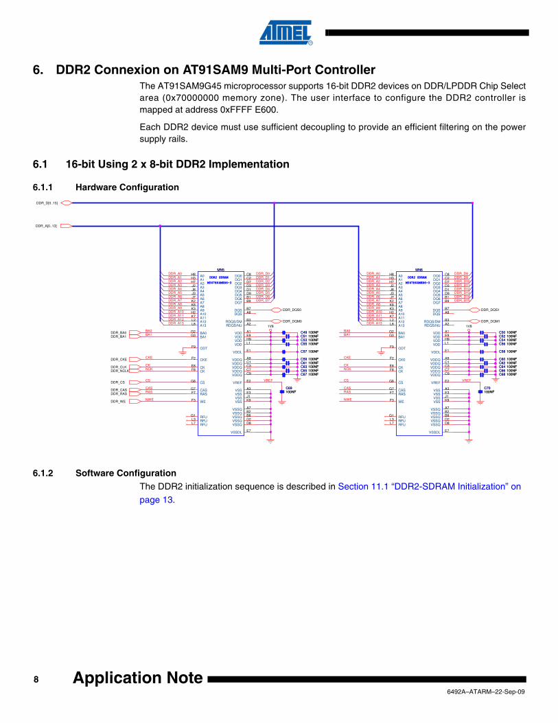
6. DDR2 Connexion on AT91SAM9 Multi-Port ControllerThe AT91SAM9G45 microprocessor supports 16-bit DDR2 devices on DDR/LPDDR Chip Selectarea (0x70000000 memory zone). The user interface to configure the DDR2 controller ismapped at address 0xFFFF E600.
Each DDR2 device must use sufficient decoupling to provide an efficient filtering on the powersupply rails.
6.1 16-bit Using 2 x 8-bit DDR2 Implementation
6.1.1 Hardware Configuration
6.1.2 Software ConfigurationThe DDR2 initialization sequence is described in Section 11.1 “DDR2-SDRAM Initialization” on
page 13.
RASCAS
NWE
CKE
DDR_D7
DDR_D3DDR_D2
DDR_D4
DDR_D0DDR_D1
DDR_D5DDR_D6
BA0BA1
DDR_A0DDR_A1DDR_A2DDR_A3DDR_A4DDR_A5DDR_A6DDR_A7DDR_A8DDR_A9DDR_A10DDR_A11DDR_A12DDR_A13
CKNCK
CS VREF VREF
CKNCK
CS
BA0BA1
RASCAS
NWE
CKE
DDR_D15
DDR_D11DDR_D10
DDR_D12
DDR_D8DDR_D9
DDR_D13DDR_D14
DDR_A0DDR_A1DDR_A2DDR_A3DDR_A4DDR_A5DDR_A6DDR_A7DDR_A8DDR_A9DDR_A10DDR_A11DDR_A12DDR_A13
DDR_RASDDR_CAS
DDR_WE
DDR_CKE
DDR_BA1DDR_BA0
DDR_NCLKDDR_CLK
DDR_CS
DDR_D[0..15]
DDR_A[0..13]
DDR_DQS1
DDR_DQM1
DDR_DQS0
DDR_DQM0
1V81V8
C58 100NFC58 100NF
C67 100NFC67 100NF
MT47H64M8B6-3
DDR2 SDRAM
MN6
MT47H64M8B6-3
DDR2 SDRAM
MN6
A0H8
A1H3
A2H7
A3J2
A4J8
A5J3
A6J7
A7K2
A8K8
A9K3
A10H2
BA0G2
ODTF9
DQ0 C8
DQ1 C2
DQ2 D7
DQ3 D3
DQ4 D1
DQ5 D9
DQ6 B1
DQ7 B9
DQS B7
DQS A8
RDQS/DM B3
RDQS/NU A2
VDD H9
VDD L1
VDDL E1
VREF E2
VDDQ C9
VSS A3
VSS E3
VDDQ A9
VDD E9
RFUG1
RFUL3
CKEF2
CKE8
CKF8
CASG7
RASF7
WEF3
CSG8
VDDQ C1
VDDQ C3
VDDQ C7
VSSQ B2
VSSQ B8
VSSQ D2
VSSQ D8
VDD A1
VSS J1
A11K7
BA1G3
A12L2
A13L8
VSS K9
VSSDL E7
VSSQ A7
RFUL7
C68 100NFC68 100NF
C63 100NFC63 100NF
C59 100NFC59 100NF
C57 100NFC57 100NF
C66 100NFC66 100NF
C53 100NFC53 100NF
C64 100NFC64 100NF
C69100NFC69100NF
C56 100NFC56 100NF
C62 100NFC62 100NF
C65 100NFC65 100NF
C70100NFC70100NF
C50 100NFC50 100NFC49 100NFC49 100NF
C54 100NFC54 100NF
C61 100NFC61 100NFC60 100NFC60 100NF
C52 100NFC52 100NFC51 100NFC51 100NF
C55 100NFC55 100NF
MT47H64M8B6-3
DDR2 SDRAM
MN5
MT47H64M8B6-3
DDR2 SDRAM
MN5
A0H8
A1H3
A2H7
A3J2
A4J8
A5J3
A6J7
A7K2
A8K8
A9K3
A10H2
BA0G2
ODTF9
DQ0 C8
DQ1 C2
DQ2 D7
DQ3 D3
DQ4 D1
DQ5 D9
DQ6 B1
DQ7 B9
DQS B7
DQS A8
RDQS/DM B3
RDQS/NU A2
VDD H9
VDD L1
VDDL E1
VREF E2
VDDQ C9
VSS A3
VSS E3
VDDQ A9
VDD E9
RFUG1
RFUL3
CKEF2
CKE8
CKF8
CASG7
RASF7
WEF3
CSG8
VDDQ C1
VDDQ C3
VDDQ C7
VSSQ B2
VSSQ B8
VSSQ D2
VSSQ D8
VDD A1
VSS J1
A11K7
BA1G3
A12L2
A13L8
VSS K9
VSSDL E7
VSSQ A7
RFUL7
86492A–ATARM–22-Sep-09
Application Note

Application Note
7. DDR2 Connexion on AT91SAM9 EBI ControllerThe AT91SAM9G45 microcontroller supports 16-bit DDR2 devices on one Chip Select area(NCS1) . The user i n te r face to con f igu re the DDR2 con t ro l l e r i s mapped a taddress 0xFFFF E400.
The 32-bit interface can be achieved by a single 32-bit SDRAM device or two 16-bit SDRAMdevices.
Each DDR2 device must use sufficient decoupling to provide an efficient filtering on the powersupply rails.
7.1 16-bit Using 2 x 8-bit DDR2 Implementation
7.1.1 Hardware Configuration
7.1.2 Software ConfigurationThe following configuration has to be performed:
• Assign the EBI CS1 to the DDR2 controller by setting the bit EBI_CS1A in the EBI Chip Select Assignment Register located in the bus matrix memory space
• Initialize the DDR2 controller accordingly to the DDR2 device and the system bus frequency.
The Data Bus Width is to be programmed to 16 bits.
The DDR2 initialization sequence is described in Section 11.1 “DDR2-SDRAM Initialization” on
page 13.
EBI1_DDR_D15
EBI1_DDR_D11EBI1_DDR_D10
EBI1_DDR_D12
EBI1_DDR_D8EBI1_DDR_D9
EBI1_DDR_D13EBI1_DDR_D14
EBI1_DDR_D7
EBI1_DDR_D3EBI1_DDR_D2
EBI1_DDR_D4
EBI1_DDR_D0EBI1_DDR_D1
EBI1_DDR_D5EBI1_DDR_D6
EBI1_DDR_A2EBI1_DDR_A3EBI1_DDR_A4EBI1_DDR_A5EBI1_DDR_A6EBI1_DDR_A7EBI1_DDR_A8EBI1_DDR_A9EBI1_DDR_A10EBI1_DDR_A11EBI1_DDR_A12EBI1_DDR_A13
EBI1_DDR_A15EBI1_DDR_A14
EBI1_DDR_A2EBI1_DDR_A3EBI1_DDR_A4EBI1_DDR_A5EBI1_DDR_A6EBI1_DDR_A7EBI1_DDR_A8EBI1_DDR_A9EBI1_DDR_A10EBI1_DDR_A11EBI1_DDR_A12EBI1_DDR_A13
EBI1_DDR_A15EBI1_DDR_A14
NCLK_EBI1
CS_EBI1
BA0_EBI1BA1_EBI1
RAS_EBI1CAS_EBI1
WE_EBI1
CKE_EBI1
CLK_EBI1NCLK_EBI1
CS_EBI1
BA0_EBI1BA1_EBI1
RAS_EBI1CAS_EBI1
WE_EBI1
CKE_EBI1
VREF1 VREF1
CLK_EBI1
EBI1_DDR_A[2..15]
NCLK_EBI1CLK_EBI1
CS_EBI1
RAS_EBI1CAS_EBI1
WE_EBI1
CKE_EBI1
BA1_EBI1BA0_EBI1
DQS0_EBI1
DQM0_EBI1
DQS1_EBI1
DQM1_EBI1
EBI1_DDR_D[0..15]
1V8 1V8
NCS1
(SDA10) (SDA10)
C87 100nFC87 100nFC85 100nFC85 100nFC83 100nFC83 100nF
C93 100nFC93 100nF
C96 100nFC96 100nF
C82 100nFC82 100nF
C91 100nFC91 100nF
MT47H64M8CF-3
DDR2 SDRAM
MN8
MT47H64M8CF-3
DDR2 SDRAM
MN8
A0H8
A1H3
A2H7
A3J2
A4J8
A5J3
A6J7
A7K2
A8K8
A9K3
A10H2
BA0G2
ODTF9
DQ0 C8
DQ1 C2
DQ2 D7
DQ3 D3
DQ4 D1
DQ5 D9
DQ6 B1
DQ7 B9
DQS B7
DQS A8
RDQS/DM B3
RDQS/NU A2
VDD H9
VDD L1
VDDL E1
VREF E2
VDDQ C9
VSS A3
VSS E3
VDDQ A9
VDD E9
RFU1G1
RFU2L3
CKEF2
CKE8
CKF8
CASG7
RASF7
WEF3
CSG8
VDDQ C1
VDDQ C3
VDDQ C7
VSSQ B2
VSSQ B8
VSSQ D2
VSSQ D8
VDD A1
VSS J1
A11K7
BA1G3
A12L2
A13L8
VSS K9
VSSDL E7
VSSQ A7
RFU3L7
C92 100nFC92 100nF
C101100nFC101100nF
C90 100nFC90 100nF
C102100nFC102100nF
C97 100nFC97 100nFC99 100nFC99 100nF
C88 100nFC88 100nF
C81 100nFC81 100nF
C84 100nFC84 100nF
C95 100nFC95 100nF
C80 100nFC80 100nF
MT47H64M8CF-3
DDR2 SDRAM
MN9
MT47H64M8CF-3
DDR2 SDRAM
MN9
A0H8
A1H3
A2H7
A3J2
A4J8
A5J3
A6J7
A7K2
A8K8
A9K3
A10H2
BA0G2
ODTF9
DQ0 C8
DQ1 C2
DQ2 D7
DQ3 D3
DQ4 D1
DQ5 D9
DQ6 B1
DQ7 B9
DQS B7
DQS A8
RDQS/DM B3
RDQS/NU A2
VDD H9
VDD L1
VDDL E1
VREF E2
VDDQ C9
VSS A3
VSS E3
VDDQ A9
VDD E9
RFU1G1
RFU2L3
CKEF2
CKE8
CKF8
CASG7
RASF7
WEF3
CSG8
VDDQ C1
VDDQ C3
VDDQ C7
VSSQ B2
VSSQ B8
VSSQ D2
VSSQ D8
VDD A1
VSS J1
A11K7
BA1G3
A12L2
A13L8
VSS K9
VSSDL E7
VSSQ A7
RFU3L7
C86 100nFC86 100nF
C98 100nFC98 100nF
C94 100nFC94 100nF
C89 100nFC89 100nF
96492A–ATARM–22-Sep-09
8. DDR2 Signal Routing ConsiderationsThe critical high speed signal is associated with the DDR2. The following are general guidelinesfor designing a DDR2 interface with AT91SAM9 products with a targeted speed of 133 MHz onSDCK/#SDCK:
• At first, position the DDR2 devices as close to the processor as possible. A longer trace will increase the rise time and the fall time of the signals. The setup time of signals generated by the AT91 Microcontroller will decrease with an increased trace length.
• Keep the DDR2 clocks and control lines as short as possible.
• Keep the DDR2 address and data lines as short as possible.
• For a proper DDR2 operation at 133 MHz, a bus impedance adaptation is necessary. 10 to 30 Ohms series resistors can be placed on all the switching signals to limit the current flow into each outputs The resistor is to be located near the processor. The need for series termination resistors and their specific value on the signals are better determined by simulation, using IBIS models and the specific design PCB layout. On SAM9G45-EKES and SAM9M10G45-EK, the adaptation is achieved with a 27-Ohm serial resistor.
• To support maximum speeds, reasonable DDR2 loading constraints must be followed. For high-speed operation, the maximum load cannot exceed 30 pF on address and data buses, and 10 pF on SDCK and #SDCK. The user must consider all the devices connected on the different buses to calculate the system load.
• Use sufficient decoupling scheme for memory devices. It is recommended to use low ESR 0.01 µF and 0.1 µF decoupling capacitors in parallel. An additional 0.001 µF decoupling capacitor is recommended to minimize ground bounce and to filter high frequency noise.
106492A–ATARM–22-Sep-09
Application Note

Application Note
9. DDR2 Electromagnetic Compatibility Improvement
9.1 Simultaneous SwitchingSimultaneous switching is the worst enemy of EMI at device operation level. TheAT91SAM9G45 microprocessor embeds Delay Controller on High Speed signals.
These delays are applied to address A[15:0] and Data D[15:0]. They are controlled in dedicatedregisters in DDR2 controller, PIO controller and Static Memory controller respectively for DDR2signal, High Speed MCI and EBI signals. Refer to the Product Datasheet for more details.
9.2 Over-ShootsOver-shoots occur when the current driven is too high. The AT91SAM9G45 microprocessorembeds drive control on memory signals. Refer to the Product Datasheet for more details.
116492A–ATARM–22-Sep-09
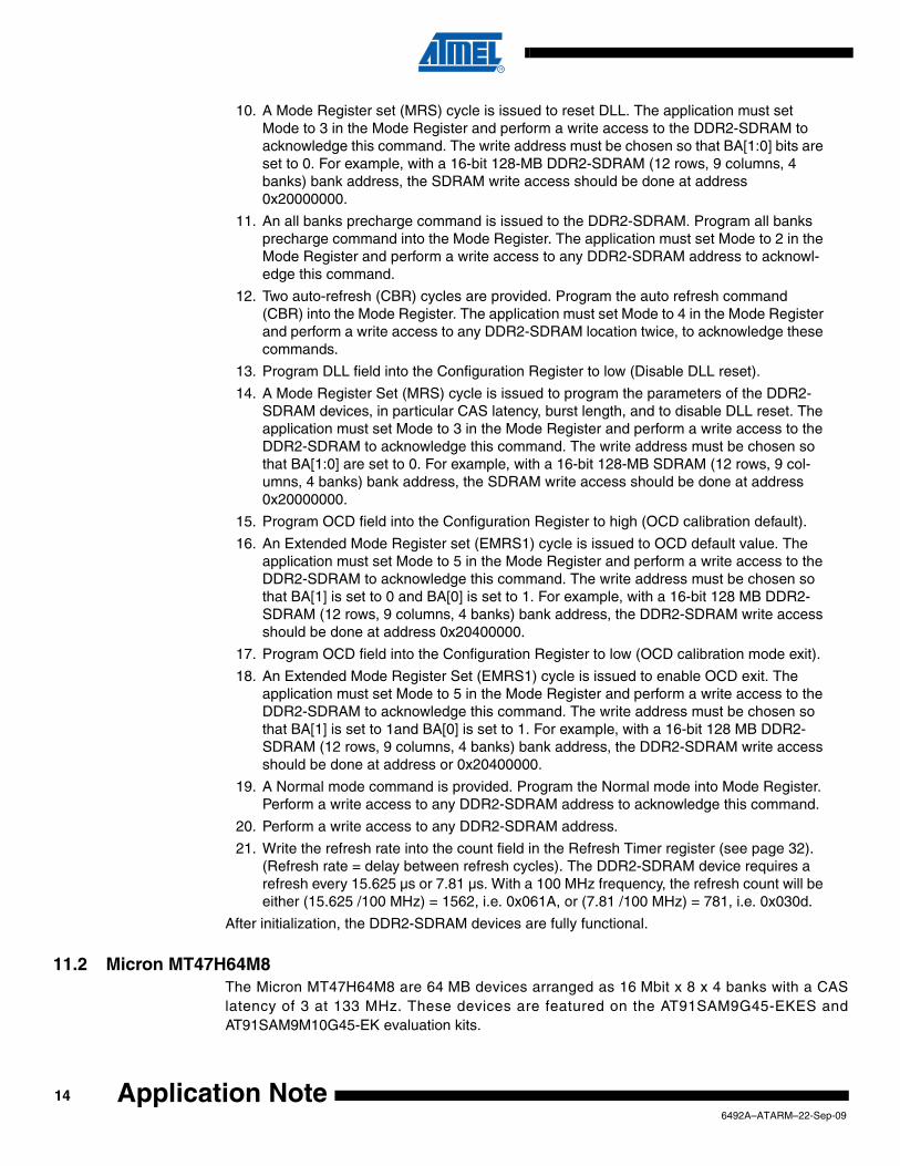
10. DDR2 VREF Signal ConsiderationsDDR_VREF is used by the input buffers of the DDR2 memories and the DDR2 controller todetermine logic levels. VREF is specified to be 0.9V (½ the power supply voltage) and is createdusing a voltage divider constructed from two 1.5 kOhm, 1% tolerance resistors.
DDR_VREF is not a high current supply, but it is important to keep it as quiet as possible withminimal inductance.
DDR_VREF DDR_VREF
1V8
R361RR361R
L7
10uH 150mA
L7
10uH 150mAR371.5KR371.5K
C77100nFC77100nF
C79100nFC79100nF
C784.7uFC784.7uF
R381.5KR381.5K
126492A–ATARM–22-Sep-09
Application Note

Application Note
11. DDR2 Controller Configuration
11.1 DDR2-SDRAM InitializationThe initialization sequence is generated by software. The DDR2-SDRAM devices are initializedby the following sequence:
(For a register description, see DDR2-SDRAM Initialization section on the AT91SAM9G45Datasheet)
(For an example of initialization, see the “Appendix” )
1. Program the memory device type into the Memory Device Register.
2. Program the DDR2-SDRAM device features into the Timing Register (asynchronous timing (TRC, TRAS, etc.)), and into the Configuration Register (number of columns, rows, banks, CAS latency and output drive strength).
3. A NOP command is issued to the DDR2-SDRAM. Program the NOP command into the Mode Register. The application must set Mode to 1 in the Mode Register and perform a write access to any DDR2-SDRAM address to acknowledge this command. Now clocks which drive DDR2-SDRAM device are enabled.
A minimum pause of 200 µs is provided to precede any signal toggle.
4. An NOP command is issued to the DDR2-SDRAM. Program the NOP command into the Mode Register. The application must set Mode to 1 in the Mode Register and per-form a write access to any DDR2-SDRAM address to acknowledge this command. Now CKE is driven high.
5. An all banks precharge command is issued to the DDR2-SDRAM. Program all banks precharge command into the Mode Register. The application must set Mode to 2 in the Mode Register and perform a write access to any DDR2-SDRAM address to acknowl-edge this command.
6. An Extended Mode Register set (EMRS2) cycle is issued to chose between commer-cial or high temperature operations. The application must set Mode to 5 in the Mode Register and perform a write access to the DDR2-SDRAM to acknowledge this com-mand. The write address must be chosen so that BA[1] is set to 1 and BA[0] is set to 0. For example, with a 16-bit 128-MB DDR2-SDRAM (12 rows, 9 columns, 4 banks) bank address, the DDR2-SDRAM write access should be done at address 0x20800000*. * This address is for example purposes only. The real address depends on the implementation in the product.
7. An Extended Mode Register set (EMRS3) cycle is issued to set all registers to “0”. The application must set Mode to 5 in the Mode Register and perform a write access to the DDR2-SDRAM to acknowledge this command. The write address must be chosen so that BA[1] is set to 1 and BA[0] is set to 1. For example, with a 16-bit 128-MB DDR2-SDRAM (12 rows, 9 columns, 4 banks) bank address, the DDR2-SDRAM write access should be done at address 0x20C00000.
8. An Extended Mode Register set (EMRS1) cycle is issued to enable DLL. The applica-tion must set Mode to 5 in the Mode Register and perform a write access to the DDR2-SDRAM to acknowledge this command. The write address must be chosen so that BA[1] and BA[0] are set to 0. For example, with a 16-bit 128-MB DDR2-SDRAM (12 rows, 9 columns, 4 banks) bank address, the DDR2-SDRAM write access should be done at address 0x20800000 or 0x20400000.
An additional 200 cycles of clock are required for locking DLL.
9. Program DLL field into the Configuration Register to high (Enable DLL reset).
136492A–ATARM–22-Sep-09
10. A Mode Register set (MRS) cycle is issued to reset DLL. The application must set Mode to 3 in the Mode Register and perform a write access to the DDR2-SDRAM to acknowledge this command. The write address must be chosen so that BA[1:0] bits are set to 0. For example, with a 16-bit 128-MB DDR2-SDRAM (12 rows, 9 columns, 4 banks) bank address, the SDRAM write access should be done at address 0x20000000.
11. An all banks precharge command is issued to the DDR2-SDRAM. Program all banks precharge command into the Mode Register. The application must set Mode to 2 in the Mode Register and perform a write access to any DDR2-SDRAM address to acknowl-edge this command.
12. Two auto-refresh (CBR) cycles are provided. Program the auto refresh command (CBR) into the Mode Register. The application must set Mode to 4 in the Mode Register and perform a write access to any DDR2-SDRAM location twice, to acknowledge these commands.
13. Program DLL field into the Configuration Register to low (Disable DLL reset).
14. A Mode Register Set (MRS) cycle is issued to program the parameters of the DDR2-SDRAM devices, in particular CAS latency, burst length, and to disable DLL reset. The application must set Mode to 3 in the Mode Register and perform a write access to the DDR2-SDRAM to acknowledge this command. The write address must be chosen so that BA[1:0] are set to 0. For example, with a 16-bit 128-MB SDRAM (12 rows, 9 col-umns, 4 banks) bank address, the SDRAM write access should be done at address 0x20000000.
15. Program OCD field into the Configuration Register to high (OCD calibration default).
16. An Extended Mode Register set (EMRS1) cycle is issued to OCD default value. The application must set Mode to 5 in the Mode Register and perform a write access to the DDR2-SDRAM to acknowledge this command. The write address must be chosen so that BA[1] is set to 0 and BA[0] is set to 1. For example, with a 16-bit 128 MB DDR2-SDRAM (12 rows, 9 columns, 4 banks) bank address, the DDR2-SDRAM write access should be done at address 0x20400000.
17. Program OCD field into the Configuration Register to low (OCD calibration mode exit).
18. An Extended Mode Register Set (EMRS1) cycle is issued to enable OCD exit. The application must set Mode to 5 in the Mode Register and perform a write access to the DDR2-SDRAM to acknowledge this command. The write address must be chosen so that BA[1] is set to 1and BA[0] is set to 1. For example, with a 16-bit 128 MB DDR2-SDRAM (12 rows, 9 columns, 4 banks) bank address, the DDR2-SDRAM write access should be done at address or 0x20400000.
19. A Normal mode command is provided. Program the Normal mode into Mode Register. Perform a write access to any DDR2-SDRAM address to acknowledge this command.
20. Perform a write access to any DDR2-SDRAM address.
21. Write the refresh rate into the count field in the Refresh Timer register (see page 32). (Refresh rate = delay between refresh cycles). The DDR2-SDRAM device requires a refresh every 15.625 µs or 7.81 µs. With a 100 MHz frequency, the refresh count will be either (15.625 /100 MHz) = 1562, i.e. 0x061A, or (7.81 /100 MHz) = 781, i.e. 0x030d.
After initialization, the DDR2-SDRAM devices are fully functional.
11.2 Micron MT47H64M8The Micron MT47H64M8 are 64 MB devices arranged as 16 Mbit x 8 x 4 banks with a CASlatency of 3 at 133 MHz. These devices are featured on the AT91SAM9G45-EKES andAT91SAM9M10G45-EK evaluation kits.
146492A–ATARM–22-Sep-09
Application Note

Application Note
The following table gives the delay in ns extracted from the DDR2-SDRAM datasheet, the corre-sponding number of cycles at 133 MHz, and the field to program these values accordingly.
Description Register/Field Value
System
PLL Frequency 800 MHz PMC_PLLAR 0x20c73f03
Processor / Bus Clock 400 / 133 MHz PMC_MCKR 0x00001302
System ClockDDR clock
enable PMC_SCER 0x00000005
EBI Chip Select Assignment DDR/SDR EBI_CSA
EBI_CS1A 0x2
DDR2 DeviceValue in
DatasheetValue in
Datasheet Register/Field Value
DDRSDRC Configuration Register DDRSDRC_CR 0x3d
Number of Columns 10 10 NC 0x1
Number of Rows 14 14 NR 0x3
CAS Latency 3 3 cycles CAS 0x3
Reset DLL Disable DLL 0x0
Output Driver Impedance control Normal DIC/DS 0x0
Disable DLL No DIS_DLL 0x0
Off-Chip Driver (1) OCD 0x0
Mask Data is shared not shared DMQS 0x0
Enable Read Measure disabled ENRDM 0x0
Delay in Datasheet
(ns)
Number of Cycles at 133 MHz Register/Field Value
DDRSDRC Timing 0 Register DDRSDRC_T0PR 0x21128226
ACTIVATE to PRECHARGE time 45 6 cycles TRAS 0x6
ACTIVATE to READ/WRITE time 15 2 cycles TRCD 0x2
Last DATA-IN to PRECHARGE time 15 2 cycles TWR 0x2
REFRESH to ACTIVATE time 55 8 cycles TRC 0x8
PRECHARGE to ACTIVATE time 15 2 cycles TRP 0x2
ACTIVE bankA to ACTIVE BankB 7.5 1 cycle TRRD 0x1
Internal Write to Read Delay 7.5 1 cycle TWTR 0x1
Load Mode Register Command to ACTIVE or REFRESH Command 2 cycles 2 cycles TMRD 0x2
DDRSDRC Timing 1 Register DDRSDRC_T1PR 0x02c8100e
Row Cycle delay 105 14 cycles TRFC 0xe
Exit Self Refresh Delay to Non-Read Command TRFC+10 16 cycles TXSNR 0x10
156492A–ATARM–22-Sep-09
Note: 1. OCD is not supported, but it is a mandatory step in the DDR2 initialization phase.
Exit Self Refresh Delay to Read Command 200 cycles 200 cycles TXSRD 0xc8
Exit Power-down Delay to First Command 2 cycles 2 cycles TXP 0x2
DDRSDRC Timing 2 RegisterDDRSDRC_T2PR
0x000001072
Exit Active Power Down Delay to Read Command (Fast Exit) 2 cycles 2 cycles TXARD 0x2
Exit Active Power Down Delay to Read Command (Slow Exit) 7 cycles TXARDS 0x7
Row Precharge All Delay 0 cycle TRPA 0x0
Read to Precharge 7.5 1 cycle TRTP 0x1
DDRSDRC Memory Device Register DDRSDRC_MD 0x00000016
Memory DeviceDDR2-SDRAM MD 0x6
Data Bus Width 16 bits DBW 0x1
SDRAM Refresh Timer Register - Timer Count 7µs SDRAMC_TR 0x410
Description Register/Field Value
166492A–ATARM–22-Sep-09
Application Note
Application Note
12. AppendixHere is an example of the DDR2 initialization code, associated to the different steps introducedin Section 11.1 “DDR2-SDRAM Initialization” on page 13:
//*----------------------------------------------------------------------------
//* \fn ddram_init
//* \brief Initialization of the DDR Controller
//*----------------------------------------------------------------------------
int ddram_init(unsigned int ddram_controller_address, unsigned int ddram_address, struct SDdramConfig *ddram_config)
{
volatile unsigned int i;
unsigned int cr = 0;
// Initialization Step 1: Program the memory device type
// Configure the DDR controller
write_ddramc(ddram_controller_address, HDDRSDRC2_MDR, ddram_config->ddramc_mdr);
// Program the DDR Controller
write_ddramc(ddram_controller_address, HDDRSDRC2_CR, ddram_config->ddramc_cr);
// Initialization Step 2: assume timings for 7.5 ns min clock period
write_ddramc(ddram_controller_address, HDDRSDRC2_T0PR, ddram_config->ddramc_t0pr);
// pSDDRC->HDDRSDRC2_T1PR
write_ddramc(ddram_controller_address, HDDRSDRC2_T1PR, ddram_config->ddramc_t1pr);
// pSDDRC->HDDRSDRC2_T2PR
write_ddramc(ddram_controller_address, HDDRSDRC2_T2PR, ddram_config->ddramc_t2pr);
// Initialization Step 3: NOP command -> allow to enable clk
write_ddramc(ddram_controller_address, HDDRSDRC2_MR, AT91C_DDRC2_MODE_NOP_CMD);
*((unsigned volatile int*) ddram_address) = 0;
// Initialization Step 3 (must wait 200 µs) (6 core cycles per iteration, core is at 396 MHz: // min 13,200 loops)
for (i = 0; i < 13300; i++) {
asm(" nop");
}
// Initialization Step 4: An NOP command is issued to the DDR2-SDRAM
// NOP command -> allow to enable cke
write_ddramc(ddram_controller_address, HDDRSDRC2_MR, AT91C_DDRC2_MODE_NOP_CMD);
*((unsigned volatile int*) ddram_address) = 0;
// wait 400 ns min
for (i = 0; i < 100; i++) {
asm(" nop");
}
176492A–ATARM–22-Sep-09
// Initialization Step 5: Set All Bank Precharge
write_ddramc(ddram_controller_address, HDDRSDRC2_MR, AT91C_DDRC2_MODE_PRCGALL_CMD);
*((unsigned volatile int*) ddram_address) = 0;
// wait 400 ns min
for (i = 0; i < 100; i++) {
asm(" nop");
}
// Initialization Step 6: Set EMR operation (EMRS2)
write_ddramc(ddram_controller_address, HDDRSDRC2_MR, AT91C_DDRC2_MODE_EXT_LMR_CMD);
*((unsigned int *)(ddram_address + 0x4000000)) = 0;
// wait 2 cycles min
for (i = 0; i < 100; i++) {
asm(" nop");
}
// Initialization Step 7: Set EMR operation (EMRS3)
write_ddramc(ddram_controller_address, HDDRSDRC2_MR, AT91C_DDRC2_MODE_EXT_LMR_CMD);
*((unsigned int *)(ddram_address + 0x6000000)) = 0;
// wait 2 cycles min
for (i = 0; i < 100; i++) {
asm(" nop");
}
// Initialization Step 8: Set EMR operation (EMRS1)
write_ddramc(ddram_controller_address, HDDRSDRC2_MR, AT91C_DDRC2_MODE_EXT_LMR_CMD);
*((unsigned int *)(ddram_address + 0x2000000)) = 0;
// wait 200 cycles min
for (i = 0; i < 10000; i++) {
asm(" nop");
}
// Initialization Step 9: enable DLL reset
cr = read_ddramc(ddram_controller_address, HDDRSDRC2_CR);
write_ddramc(ddram_controller_address, HDDRSDRC2_CR, cr | AT91C_DDRC2_DLL_RESET_ENABLED);
// Initialization Step 10: reset DLL
write_ddramc(ddram_controller_address, HDDRSDRC2_MR, AT91C_DDRC2_MODE_EXT_LMR_CMD);
*(((unsigned volatile int*) ddram_address)) = 0;
// wait 2 cycles min
for (i = 0; i < 100; i++) {
asm(" nop");
}
186492A–ATARM–22-Sep-09
Application Note

Application Note
// Initialization Step 11: Set All Bank Precharge
write_ddramc(ddram_controller_address, HDDRSDRC2_MR, AT91C_DDRC2_MODE_PRCGALL_CMD);
*(((unsigned volatile int*) ddram_address)) = 0;
// wait 400 ns min
for (i = 0; i < 100; i++) {
asm(" nop");
}
// Initialization Step 12: Two auto-refresh (CBR) cycles are provided. Program the auto refresh // command (CBR) into the Mode Register.
write_ddramc(ddram_controller_address, HDDRSDRC2_MR, AT91C_DDRC2_MODE_RFSH_CMD);
*(((unsigned volatile int*) ddram_address)) = 0;
// wait 10 cycles min
for (i = 0; i < 100; i++) {
asm(" nop");
}
// Set 2nd CBR
write_ddramc(ddram_controller_address, HDDRSDRC2_MR, AT91C_DDRC2_MODE_RFSH_CMD);
*(((unsigned volatile int*) ddram_address)) = 0;
// wait 10 cycles min
for (i = 0; i < 100; i++) {
asm(" nop");
}
// Initialization Step 13: Program DLL field into the Configuration Register to low (Disable // DLL reset).
cr = read_ddramc(ddram_controller_address, HDDRSDRC2_CR);
write_ddramc(ddram_controller_address, HDDRSDRC2_CR, cr & (~AT91C_DDRC2_DLL_RESET_ENABLED));
// Initialization Step 14: A Mode Register set (MRS) cycle is issued to program the parameters // of the DDR2-SDRAM devices.
write_ddramc(ddram_controller_address, HDDRSDRC2_MR, AT91C_DDRC2_MODE_LMR_CMD);
*(((unsigned volatile int*) ddram_address)) = 0;
// Initialization Step 15: Program OCD field into the Configuration Register to high (OCD // calibration default).
cr = read_ddramc(ddram_controller_address, HDDRSDRC2_CR);
write_ddramc(ddram_controller_address, HDDRSDRC2_CR, cr | AT91C_DDRC2_OCD_DEFAULT);
// Initialization Step 16: An Extended Mode Register set (EMRS1) cycle is issued to OCD default // value.
write_ddramc(ddram_controller_address, HDDRSDRC2_MR, AT91C_DDRC2_MODE_EXT_LMR_CMD);
*(((unsigned int*) (ddram_address + 0x2000000))) = 0;
// wait 2 cycles min
for (i = 0; i < 100; i++) {
asm(" nop");
}
196492A–ATARM–22-Sep-09
// Initialization Step 17: Program OCD field into the Configuration Register to low (OCD // calibration mode exit).
cr = read_ddramc(ddram_controller_address, HDDRSDRC2_CR);
write_ddramc(ddram_controller_address, HDDRSDRC2_CR, cr & (~AT91C_DDRC2_OCD_EXIT));
// Initialization Step 18: An Extended Mode Register set (EMRS1) cycle is issued to enable OCD // exit.
write_ddramc(ddram_controller_address, HDDRSDRC2_MR, AT91C_DDRC2_MODE_EXT_LMR_CMD);
*(((unsigned int*) (ddram_address + 0x6000000))) = 0;
// wait 2 cycles min
for (i = 0; i < 100; i++) {
asm(" nop");
}
// Initialization Step 19, 20: A mode Normal command is provided. Program the Normal mode into // Mode Register.
write_ddramc(ddram_controller_address, HDDRSDRC2_MR, AT91C_DDRC2_MODE_NORMAL_CMD);
*(((unsigned volatile int*) ddram_address)) = 0;
// Initialization Step 21: Write the refresh rate into the count field in the Refresh Timer // register. The DDR2-SDRAM device requires a refresh every 15.625 ¦µs or 7.81 ¦µs. With a // 100MHz frequency, the refresh timer count register must to be set with (15.625 x 100 MHz) = // 1562 i.e. 0x061A or (7.81 x 100MHz) = 781 i.e. 0x030d.
// Set Refresh timer
write_ddramc(ddram_controller_address, HDDRSDRC2_RTR, ddram_config->ddramc_rtr);
// OK, now we are ready to work on the DDRSDR
// wait for the end of calibration
for (i = 0; i < 500; i++) {
asm(" nop");
}
return 0;
}
206492A–ATARM–22-Sep-09
Application Note
Application Note
Revision History
Doc. Rev CommentsChange Request Ref.
6492A First issue
216492A–ATARM–22-Sep-09
Headquarters International
Atmel Corporation2325 Orchard ParkwaySan Jose, CA 95131USATel: 1(408) 441-0311Fax: 1(408) 487-2600
Atmel AsiaUnit 1-5 & 16, 19/FBEA Tower, Millennium City 5418 Kwun Tong RoadKwun Tong, KowloonHong KongTel: (852) 2245-6100Fax: (852) 2722-1369
Atmel EuropeLe Krebs8, Rue Jean-Pierre TimbaudBP 30978054 Saint-Quentin-en-Yvelines CedexFranceTel: (33) 1-30-60-70-00 Fax: (33) 1-30-60-71-11
Atmel Japan9F, Tonetsu Shinkawa Bldg.1-24-8 ShinkawaChuo-ku, Tokyo 104-0033JapanTel: (81) 3-3523-3551Fax: (81) 3-3523-7581
Product Contact
Web Sitewww.atmel.comwww.atmel.com/AT91SAM
Technical SupportAT91SAM SupportAtmel techincal support
Sales Contactswww.atmel.com/contacts/
Literature Requestswww.atmel.com/literature
Disclaimer: The information in this document is provided in connection with Atmel products. No license, express or implied, by estoppel or otherwise, to anyintellectual property right is granted by this document or in connection with the sale of Atmel products. EXCEPT AS SET FORTH IN ATMEL’S TERMS AND CONDI-TIONS OF SALE LOCATED ON ATMEL’S WEB SITE, ATMEL ASSUMES NO LIABILITY WHATSOEVER AND DISCLAIMS ANY EXPRESS, IMPLIED OR STATUTORYWARRANTY RELATING TO ITS PRODUCTS INCLUDING, BUT NOT LIMITED TO, THE IMPLIED WARRANTY OF MERCHANTABILITY, FITNESS FOR A PARTICULARPURPOSE, OR NON-INFRINGEMENT. IN NO EVENT SHALL ATMEL BE LIABLE FOR ANY DIRECT, INDIRECT, CONSEQUENTIAL, PUNITIVE, SPECIAL OR INCIDEN-TAL DAMAGES (INCLUDING, WITHOUT LIMITATION, DAMAGES FOR LOSS OF PROFITS, BUSINESS INTERRUPTION, OR LOSS OF INFORMATION) ARISING OUTOF THE USE OR INABILITY TO USE THIS DOCUMENT, EVEN IF ATMEL HAS BEEN ADVISED OF THE POSSIBILITY OF SUCH DAMAGES. Atmel makes norepresentations or warranties with respect to the accuracy or completeness of the contents of this document and reserves the right to make changes to specificationsand product descriptions at any time without notice. Atmel does not make any commitment to update the information contained herein. Unless specifically providedotherwise, Atmel products are not suitable for, and shall not be used in, automotive applications. Atmel’s products are not intended, authorized, or warranted for useas components in applications intended to support or sustain life.
© 2009 Atmel Corporation. All rights reserved. Atmel®, Atmel logo and combinations thereof, and others are registered trademarks or trade-marks of Atmel Corporation or its subsidiaries. Other terms and product names may be trademarks of others.
6492A–ATARM–22-Sep-09


![AT91SAM - Keil · 2013. 1. 23. · SAM4S Series Preliminary Datasheet 11100B–ATARM–31-Jul-12. 2 11100B–ATARM–31-Jul-12 SAM4S Series [Preliminary] 1. Description The Atmel](https://static.fdocuments.us/doc/165x107/6145497b34130627ed50e179/at91sam-keil-2013-1-23-sam4s-series-preliminary-datasheet-11100baatarma31-jul-12.jpg)


![AT24C256C - ww1.microchip.comww1.microchip.com/downloads/en/DeviceDoc/Atmel-8568-SEEPROM-AT24C25… · AT24C256C [DATASHEET] Atmel-8568F-SEEPROM-AT24C256C-Datasheet_012015 6 6. Device](https://static.fdocuments.us/doc/165x107/5e19dbf9d55cfc7fce018509/at24c256c-ww1-at24c256c-datasheet-atmel-8568f-seeprom-at24c256c-datasheet012015.jpg)