Appendice assoluti pagine 1-5 - Ermec - Distribución de ... description 4 CODES EXAMPLE: Natural...
28
Gray code CODES CHARACTERISED BY SEVERAL CHANGES A STEP 1) BINARY NATURAL CODE The Binary Natural code is characterised by two switching levels: TRANSPARENT/DARK, OFF/ON, 0/1, etc. The code is generally represented by a “1” or a “0”. The graphic representations of “1” and “0” are called “Bit”, and are directly related to binary arithmetics. Every value can be represented with a sequence of several Bit from “1” or from “0”. Each Bit of the binary sequence has a fixed position value: n from 2 ° to 2 . This value is equal to 2 raised to the power indicated by the position itself (Fig. 1). 2) BCD CODE (8-4-2-1) Converting a decimal number into a binary value and vice versa is a very complex operation. The BCD or 8-4-2-1 code allows the direct coding of the single digits of the decimal numeration (Fig.2). Devices such as counters, position displays, etc, operate according to this code. Several Bit can change simultaneously with the a.m. codes. This can be observed for example when passing from value 7 to value 8 (Fig. 1-2). If switching is not carried out at exactly the same time, some errors in evaluation may arise. AMBIGUITY is an inherent error in encoder caused by the fact that two “on/off” measuring devices cannot generate and therefore transfer states at precisely the identical instant each and every time. In order to avoid this problem, different codes with a single change per step can be used. Examples of codes such as these are GRAY and GRAY EXCESS 3 than can be used respectively as options for the BINARY CODE and the BCD CODE. Fig.3 shows the ambiguity errors that can be found in codes different from GRAY. To avoid these errors TEKEL's absolute encoders read pattern in GRAY code or similar (see Fig. 4): the “memories” automatically change the states with the appropriate code. 1 Issue 09/1999 Codes description Fig. 1 Fig. 2 Fig. 3 Fig. 4 MSB Most Significant Bit Example of factorisation of the Decimal number “11”. 3 2 1 0 1x2 +0x2 +1x2 +1x2 = 8 + 0 + 2 + 1 = 1 1 Every digit can be represented adding further bit up to 2” 0 1 2 3 4 5 6 7 8 9 10 11 12 0 0 0 0 0 0 0 0 0 0 0 0 0 0 0 0 0 0 0 0 0 1 1 1 1 1 0 0 0 0 1 1 1 1 0 0 0 0 1 0 0 1 1 0 0 1 1 0 0 1 1 0 0 1 0 1 0 1 0 1 0 1 0 1 0 0 0 0 0 0 0 0 0 0 0 0 0 0 0 0 0 0 0 0 0 0 1 1 1 1 1 0 0 0 0 1 1 1 1 1 1 1 1 0 0 0 1 1 1 1 0 0 0 0 1 1 1 0 1 1 0 0 1 1 0 0 1 1 0 0 4 2 3 2 2 2 1 2 0 2 0 0 0 0 0 0 0 0 0 0 1 1 1 0 0 0 0 0 0 0 0 1 1 0 0 0 0 0 0 0 1 1 1 1 0 0 0 0 0 0 0 1 1 0 0 1 1 0 0 0 0 1 0 1 0 1 0 1 0 1 0 1 0 1 0 POSITION GRAY BINARY BCD Bit Decimal values 3 2 =8 2 2 =4 1 2 =2 0 2 =1 15 14 13 12 11 10 9 8 7 6 5 4 3 2 1 0 BINARY NATURAL CODE Bit Decimal values 3 2 =8 2 2 =4 1 2 =2 0 2 =1 9 8 7 6 5 4 3 2 1 0 BCD CODE (o 8 - 4 - 2 - 1) 0 1 2 3 4 5 6 7 8 9 10 11 12 13 14 15 175
Transcript of Appendice assoluti pagine 1-5 - Ermec - Distribución de ... description 4 CODES EXAMPLE: Natural...

Gray code
CODES CHARACTERISED BY SEVERAL CHANGES A STEP
1) BINARY NATURAL CODEThe Binary Natural code is characterised by two switching levels: TRANSPARENT/DARK, OFF/ON, 0/1, etc.The code is generally represented by a “1” or a “0”. The graphic representations of “1” and “0” are called “Bit”, and are directly related to binary arithmetics.Every value can be represented with a sequence of several Bit from “1” or from “0”. Each Bit of the binary sequence has a fixed position value:
nfrom 2 ° to 2 . This value is equal to 2 raised to the power indicated by the position itself (Fig. 1).
2) BCD CODE (8-4-2-1)Converting a decimal number into a binary value and vice versa is a very complex operation. The BCD or 8-4-2-1 code allows the direct coding of the single digits of the decimal numeration (Fig.2). Devices such as counters, position displays, etc, operate according to this code.
Several Bit can change simultaneously with the a.m. codes. This can be observed for example when passing from value 7 to value 8 (Fig. 1-2). If switching is not carried out at exactly the same time, some errors in evaluation may arise.AMBIGUITY is an inherent error in encoder caused by the fact that two “on/off” measuring devices cannot generate and therefore transfer states at precisely the identical instant each and every time. In order to avoid this problem, different codes with a single change per step can be used. Examples of codes such as these are GRAY and GRAY EXCESS 3 than can be used respectively as options for the BINARY CODE and the BCD CODE. Fig.3 shows the ambiguity errors that can be found in codes different from GRAY. To avoid these errors TEKEL's absolute encoders read pattern in GRAY code or similar (see Fig. 4): the “memories” automatically change the states with the appropriate code.
1Issue 09/1999
Codes description
Fig. 1
Fig. 2
Fig. 3Fig. 4
MSBMostSignificantBit
Example of factorisation of the D e c i m a l n u m b e r “ 1 1 ” .
3 2 1 01 x 2 + 0 x 2 + 1 x 2 + 1 x 2 =8 + 0 + 2 + 1 = 1 1Every digit can be representedadding further bit up to 2”
0123456789101112
0000000000000
0000000011111
0000111100001
0011001100110
0101010101010
0000000000000
0000000011111
0000111111110
0011110000111
0110011001100
42 32 22 12 02
0000000000111
0000000011000
0000111100000
0011001100001
0101010101010
POSITIONGRAY BINARY BCD
Bit
Decimal values
32 =822 =412 =202 =1
1514131211109876543210
BINARY NATURAL CODE
Bit
Decimal values
32 =822 =412 =202 =1
9876543210
BCD CODE (o 8 - 4 - 2 - 1)
0
1
2
3
4
5
6
78
9
10
11
12
13
14
15
175
Codes description
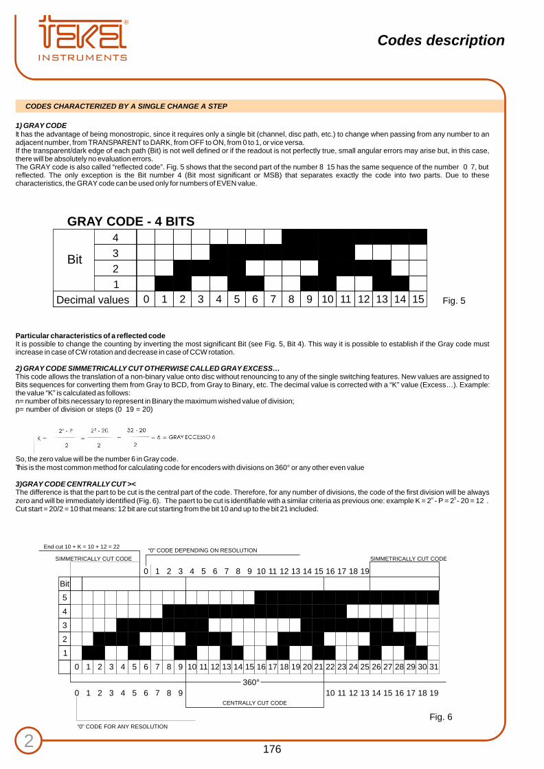
2
CODES CHARACTERIZED BY A SINGLE CHANGE A STEP
1) GRAY CODEIt has the advantage of being monostropic, since it requires only a single bit (channel, disc path, etc.) to change when passing from any number to an adjacent number, from TRANSPARENT to DARK, from OFF to ON, from 0 to 1, or vice versa.If the transparent/dark edge of each path (Bit) is not well defined or if the readout is not perfectly true, small angular errors may arise but, in this case, there will be absolutely no evaluation errors.The GRAY code is also called “reflected code”. Fig. 5 shows that the second part of the number 8 15 has the same sequence of the number 0 7, but reflected. The only exception is the Bit number 4 (Bit most significant or MSB) that separates exactly the code into two parts. Due to these characteristics, the GRAY code can be used only for numbers of EVEN value.
Particular characteristics of a reflected codeIt is possible to change the counting by inverting the most significant Bit (see Fig. 5, Bit 4). This way it is possible to establish if the Gray code must increase in case of CW rotation and decrease in case of CCW rotation.
2) GRAY CODE SIMMETRICALLY CUT OTHERWISE CALLED GRAY EXCESS…This code allows the translation of a non-binary value onto disc without renouncing to any of the single switching features. New values are assigned to Bits sequences for converting them from Gray to BCD, from Gray to Binary, etc. The decimal value is corrected with a “K” value (Excess…). Example: the value “K” is calculated as follows: n= number of bits necessary to represent in Binary the maximum wished value of division;p= number of division or steps (0 19 = 20)
So, the zero value will be the number 6 in Gray code.This is the most common method for calculating code for encoders with divisions on 360° or any other even value
3)GRAY CODE CENTRALLY CUT ><The difference is that the part to be cut is the central part of the code. Therefore, for any number of divisions, the code of the first division will be always
n 5 zero and will be immediately identified (Fig. 6). The paert to be cut is identifiable with a similar criteria as previous one: example K = 2 - P = 2 - 20 = 12 . Cut start = 20/2 = 10 that means: 12 bit are cut starting from the bit 10 and up to the bit 21 included.
Fig. 5
Bit
Decimal values
4
3
2
1
1514131211109876543210
GRAY CODE - 4 BITS
Fig. 6
313029282726252423222120191817161514131211109876543210
1
2
3
4
5
Bit
191817161514131211109876543210
9876543210 19181716151413121110
End cut 10 + K = 10 + 12 = 22
SIMMETRICALLY CUT CODE
“0” CODE DEPENDING ON RESOLUTION
SIMMETRICALLY CUT CODE
CENTRALLY CUT CODE
360°
“0” CODE FOR ANY RESOLUTION
176

3
Codes description
4) GRAY CODE EXC 3It is a decimal code that follows the a.m. rule of code Gray Excess..As in BCD code, the digits are coded from 0 to 9, therefore 4 Bits are necessary to constitute each decimal digit.The code structure is: a single change per step and, like the Gray code, it cannot be directly evaluated.
Fig. 7
Bit
D
C
B
A
0 1 2 3 4 5 6 7 8 9
Bit
D
C
B
A
0 1 2 3 4 5 6 7 8 9 0 1 2 3 4 5 6 7 8 9
GRAY CODE EXC 3FOR 100 DIVISION (0÷99)
TO FURTHERDECADE
The sequence is repeated for 5 times(20÷29; 30÷39; 40÷49; 50÷59; ect.)
EVEN DECADE ODD DECADE
177

Codes description
4
CODES EXAMPLE: Natural binary BCD Gray Excess 3
ABSOLUTE ENCODERS are divided in two major groups:SINGLE TURN: absolute encoders with a capacity equal to the resolution (i.e. 2048)MULTI TURN: absolute encoders with a capacity equal to the single turn resolution multiplied by the number of turns (i.e. 8192x 4096)
TYPICAL APPLICATIONS ! Turrets positioning!Plotter axis X-Y-Z positioning!Rotary tables positioning! Level measurements ! Length measurements for wood and metal processing!Printing machines synchronism!Radar antennas positioning! Telescopes positioning! Industrial robotics! Timing and pressing machines control!Speed control!Numerically-controlled machine tools!Crane control and positioning!Cylinder memory control!Automating computing scales!Electronic cams and valves!Nuclear-hydraulic power plants control!Production and assembling lines (ex. car industry)
GENERAL CONVENTIONS
! Code and sense of rotationThe value of code increases with CW of shaft as viewed from encoder shaft end.
! Logicpositive logic (or code): Logic “1” = “HIGH” output voltage levelLogic “0” = “LOW” output voltage levelnegative logic (or code)Logic “1” = “LOW” output voltage levelLogic “0” = “HIGH” output voltage level
Fig. 8
178
Decimalnumber
GRAY BINARY BINARY DECIMAL (BCD) GRAY EXC 3
CODE PATTERN CODE PATTERN
PATTERNCODE
2° decade 1° decade 2° decade 1° decade 2° decade 1° decade 2° decade 1° decade
PATTERNCODE

5
ABSOLUTE ENCODERInterfaces Electrical Characteristcs (Electronic)
NPN (NEGATIVE LOGIC)
PNP (POSITIVE LOGIC)
NPN - 7406 (NEGATIVE LOGIC)
NPN - 7407 (POSITIVE LOGIC)
Order code12 NPN open collector13 NPN with internal pull-up
Order code10 NPN open collector11 NPN con pull-up internal
Order code20 PNP open collector21 PNP con pull-down internal
Order code22 NPN open collector23 NPN con pull-up internal
Order code 30
l out (SINK) 100 mA max V out LOW 1,1 V max (a 100 mA)
HIGH Vcc (with pull-up resistor) Pull-up resistor (RL) 5 Vcc RL = 680 Ohm 11÷30 Vcc RL = 4K7 Ohm
PUSH-PULL (POSITIVE LOGIC)
*l out (SOURCE) 100 mA maxV out HIGH Vcc -1,8 V min (a 100 mA)
LOW 0,2 V max (with pull-up resistor)Pull-down resistor (RL) 5 Vcc RL = 680 Ohm 11÷30 Vcc RL = 4K7 Ohm
l out (SINK) 40 mA max
V out HIGH Vcc (with pull-up resistor) LOW 0,7 V max (a 40 mA)
Pull-up resistor (RL) 5 Vcc RL = 680 Ohm 11÷30 Vcc RL = 4K7 Ohm
5 Vcc PP 11÷30 Vccl out (SINK o SOURCE) 15 mA max V out HIGH= Vcc -1V (a 15 mA)LOW= 1V max (a 15 mA)
179

6
0 Volt0 Volt
+ Vcc
150 Ohm
0 Volt0 Volt
OutputOpencollector
150 Ohm
TTL OUTPUTS Ordering code 00, 01, 02, 03
NPN INPUT - Ordering code L - U - M - T
PNP INPUT Ordering code P - W - C - X - N
V Low (a 12 mA) = 0,25÷0,5 VV High (a 12 mA) = 2,4÷3,1 VI max = 2,5 mA
I max =15 mAI min = 6 mAV max = 50 Vcc
I max = 15 mAI min = 6 mAV max = 50 Vcc
+ 5 Vcc
Logic TTL
+ 5 Vcc
Output
0 Volt0 Volt
100 Ohm
ABSOLUTE ENCODER Interfaces Electrical Characteristcs (Electronic)
180

DescriptionThe absolute encoder equipped with an analogical interface is usually connected to devices (PLC) provided with an analogical A/D/C converter. The connection occurs by means of a screened cable with a maximum of 8 conductors divided as follows: 2 conductors for the analogical signal (+L, -L), 2 conductors for power, 1 conductor for the up/down selection, 3 conductors for optional signals (STROBE, ZERO and CASE).The analogical interface works with GRAY coded discs. This is then converted in a 10 Bits BINARY code by static logic circuits and then sent to a DAC. The output analogical signal of the converter is then amplified to obtain from the interface a modulated current or voltage signal. The current modulation version (4÷20 mA) has the function of controlling current in a line whose total resistance is generally 250 Ohm. The modulation occurs in such a way that, with the encoder set to zero code, on the line there is a current of 4 mA. This will gradually increase to reach 20 mA when the encoder will be in position 1023 code. The current increase is of 0.0156 mA for each encoder displacement step.The voltage modulation versions behave similarly to the 4÷20 mA version: when the encoder is in zero position the output voltage on the line will be 1 Volt, 0 Volt, - 5 Volt or 10 Volt; it will reach the values of 5 Volt, 10 Volt, 10 Volt, +5 Volt or +10 Volt when the encoder will be in 1023 position. The above mentioned values correspond to the single characteristics of the analogical interface versions 1÷5 Volt, 0÷10 Volt, 5 Volt and 10 Volt. Unlike the 4÷20 mA version, the line employed with this version will have a very high total resistance so to avoid a voltage drop which would alter the actual value of the signal. In Fig. 28 and 29 the connections for the different voltages are shown. Particular attention must be paid to the connections of the cables' screens both for applications with PLC power supply and for encoders with a separate power supply.
EXAMPLE OF APPLICATION
Fig. 9
Fig. 11
VOLTAGE SOURCE
SOURCE TYPICAL CONNECTION (4 ÷ 20 mA)
Fig. 10
Fig. 12
RESOLUTIONS
7Issue 09/1999
ABSOLUTE ENCODERS - Analog OutputInterfaces Electrical Characteristcs
181
AbsoluteEncoder
AbsoluteEncoder
AbsoluteEncoder
Supply
Supply
Supply
R = 250 Ohm tipical
Supply external or P.L.C.
1° possibility
2° possibility
8
ABSOLUTE ENCODERS - Bus Connection
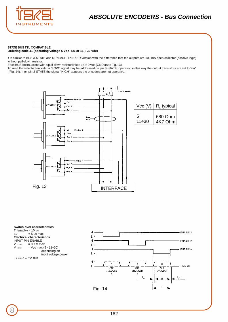
STATE BUS TTL COMPATIBLEOrdering code 41 (operating voltage 5 Vdc 5% or 11 ÷ 30 Vdc)
It is similar to BUS 3-STATE and NPN MULTIPLEXER version with the difference that the outputs are 100 mA open collector (positive logic) without pull-down resistor.Each BUS line must end with a pull-down resistor linked up to 0 Volt (GND) (see Fig. 13).To read the selected encoder a “LOW” signal may be addressed on pin 3-STATE: operating in this way the output transistors are set to “on” (Fig. 14). If on pin 3-STATE the signal “HIGH” appears the encoders are not operative.
Switch-over characteristicsT (enable) > 10 µst off = 5 µs maxElectrical characteristics INPUT PIN ENABLEV I LOW = 0,7 V maxV I HIGH = Vcc max (5 - 11÷30)
depending on input voltage power
I I HIGH > 1 mA min
Fig. 13
Fig. 14
Vcc (V)
511÷30
R L
680 Ohm4K7 Ohm
typical
182
INTERFACE
9
ABSOLUTE ENCODERS - Bus Connection
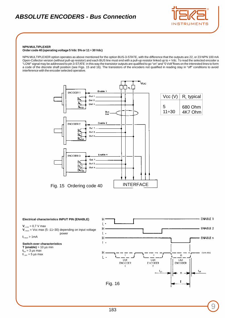
NPN MULTIPLEXEROrder code 40 (operating voltage 5 Vdc 5% or 11 ÷ 30 Vdc)
NPN MULTIPLEXER option operates as above mentioned for the option BUS-3-STATE, with the difference that the outputs are 22, or 23 NPN 100 mA Open-Collector version (without pull-up resistor) and each BUS line must end with a pull-up resistor linked up to + Vdc. To read the selected encoder a “LOW” signal may be addressed to pin 3-STATE: in this way the transistor outputs are qualified to go “on” and “0 Volt”flows on the interested lines to form a code of the discrete shaft position (see Figs. 15 and 16). The transistors of the encoders not qualified in reading stay in “off” conditions to avoid interference with the encoder selected operative.
Electrical characteristics INPUT PIN (ENABLE)
V = 0,7 V maxI LOW
V = Vcc max (5 -11÷30) depending on input voltage I HIGH
powerI > 1mAI HIGH
Switch-over characteristicsT (enable) > 10 µs mint = 3 µs maxON
t = 5 µs max OFF
Fig. 15 Ordering code 40
Fig. 16
Vcc (V)
511÷30
R L
680 Ohm4K7 Ohm
typical
183
INTERFACE
10
ABSOLUTE ENCODERS - Bus Connection
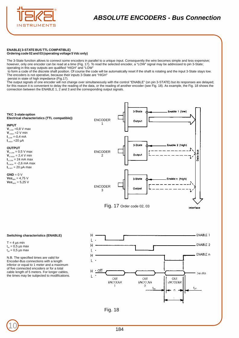
ENABLE( 3-STATE BUS TTL COMPATIBLE)Ordering code 02 and 03 (operating voltage 5 Vdc only)
The 3-State function allows to connect some encoders in parallel to a unique input. Consequently the wire becomes simple and less expensive; however, only one encoder can be read at a time (Fig. 17). To read the selected encoder, a “LOW” signal may be addressed to pin 3-State; operating in this way outputs are qualified “HIGH” and “LOW” to form a code of the discrete shaft position. Of course the code will be automatically reset if the shaft is rotating and the input 3-State stays low. The encoders is not operative, because their inputs 3-State are “HIGH” persist in state of high impedance (Fig.17).The output signals of one encoder will not change over simultaneously with the control “ENABLE” (on pin 3-STATE) but its responses are delayed; for this reason it is convenient to delay the reading of the data, or the reading of another encoder (see Fig. 18). As example, the Fig. 18 shows the connection between the ENABLE 1, 2 and 3 and the corresponding output signals.
TKC 3-state optionElectrical characteristics (TTL compatible))
INPUTV =0,8 V maxI LOW
V =2 V minI HIGH
I =-0,4 mAI LOW
I =20 µAI HIGH
OUTPUTV = 0,5 V maxO LOW
V = 2,4 V minO HIGH
I = 24 mA maxO LOW
I = -2,6 mA maxO HIGH
I = 20 µA maxO OFF
GND = 0 VVcc = 4,75 VMIN
Vcc = 5,25 VMAX
Switching characteristics (ENABLE)
T = 4 µs mint = 0,5 µs maxon
t = 0,5 µs maxoff
N.B. The specified times are valid for Encoder-Bus connections with a length inferior or equal to 1 meter and a maximum of five connected encoders or for a total cable length of 5 meters. For longer cables, the times may be subjected to modifications.
Fig. 17 02, 03 Order code
Fig. 18
ENCODER1
ENCODER2
ENCODER3
184

GENERAL CHARACTERISTICS
11
Absolute EncoderElectrical characteristics - SSI interface
“SSI” ORIGIN
The technological evolution in the 90' which has been applied on numerical controlled machines has generated a request for always more precision of acquirement of the position of the rotating shafts also for high number of turns. This requirement has been satisfied by encoder manufacturers, with an increment of measuring resolution available on single- and multiturn absolute encoders. Industry has got therefore very high precision instruments, fully suitable for the measuring needs but with the inconvenient of the high number of connections to be made for the connection for the encoder to the control system. (Tekel is manufacturing multiturn encoders with resolutions up to 8192 steps per turn x 4096 turns which supply on output 25 signal bit, to which same quantity of integrated conductors with power supply and input and output optional signals must correspond .In order to reduce the installation costs and in order to simplify the connections the synchronus serial interface , better know as SSI, has been developed and is catching always higher interest from industry.
ADVANTAGES OF “SSI” APPLICATION
The SSI application has immediately given advantages for the user such as:! easier wiring with the use of only 6 screened conductors for
any possible resolution request! possibility to update of the resolution of an existing machinery
without expensive wiring modifications! reliability of the code with Gray format! extreme simplicity and low cost for the conversion of the Gray
code into Binary (please refer to page 14)! possibility to adapt the encoder transmission speed depending
from the transmission distance! further reduction of the connections quantity thanks to the
possibility to use only one CLOCK (2 conducers) for a group of encoders each of which transmits on his own double wire possibility to determine the time and the transmission speed directly from the control board.
FUNCIONING PRINCIPALS
The optical code reading systems includes one or more coded disks, gives constantly the updated position values. The generated code is presented on the input of a parallel/serial converter (P/S) controlled on synchronus mode by a ckock frequence received on the CKI and CKI inputs )see figure on page 10).These signals do assume on rest state the logic value “1” or “high”, the controller asks the encoder for information on his position by sending a train of clock pulses which number depends from the number of bits which have to be transmitted (encoder resolution) and from the activated transmission protocol. At the first LOW/HIGH transition the code at converter P/S input is loaded; the next “LOW-HIGH” transaction gives on P/S converter output, the MSB code. Each subsequent trains pulse “LOW/HIGH” transaction gives the next bit on the line OUT.At the end of the pulses sequence established by the protocol used, and after a minimum time corresponding to ½ clock pulse, the output goes back to rest state allowing the continuous update of the data in the P/S converter.
185
PARALLEL DATA - ENCODER POSITION -
SERIAL DATA M SERIAL DATA M+2
N. BIT GRAY CODE

BLOCK DIAGRAM
TECHNICAL CHARACTERISTICS
12
Absolute EncoderElectrical characteristics - SSI interface
INPUT CLOCK (CKI, CKI)
Input type .....................................................................Minimal Frequency ......................................................Maximal Frequency .....................................................Minimal current @ 1,1 MHz .........................................Maximal current ...........................................................Line status at rest state (not on transmission) .............
OUTPUT DATA (OUT, OUT)
Output signal type .......................................................Transmission levels .....................................................Line driver type ............................................................Line status at rest state (not on transmission) .............Transmitted code type .................................................
CONNECTIONS
Number of required conducers .....................................
Connecting cable characteristics ..................................Allowed transmission distance .....................................Baud Rate (influences the transmission distance) .......
TRANSMISSION PROTOCOL
Max number of transmitted bit ......................................Max resolution of transmitted data ................................Supported transmission formats ...................................Transmission time ........................................................
complemented signals100 kHz1100 kHz6,6 mA20 mA1 logic (CKI =HIGH, CKI = LOW)
complementedcompatible with RS42226LS311 logic (OUT = HIGH , OUT = LOW)standard: Gray
4 + 2 supply + ground (not depending from numberof resolutions bits)3 twisteed shielded double cable 25, 50, 100, 200, 400 m800, 400, 300, 200, 100 kHz
268192 PPR x 4096 RPM13, 21, 24, 25, 26 right, left or center justifiedTp = 0,5 ÷ 10 µs (clock frequency function)Td = 1/2 Tp + 2 µsTr = 12 ÷ 25 µs (clock frequency function)
186
CODE DISC
LIGHT EMITTER
LIGHT RECEIVERSCHMITT TRIGGER
LINE DRIVER (RS442)
OPTO-COUPLER
CONTROLLERCONTROL INPUT
PARALLEL/SERIAL CONVERTER
TRANSMISSION PROTOCOL
N12
1 2 3 4 5 6 7 8 9 10 11 12 13 14 15 16 17 18 19 20 21 22 23 24 25
0
0 0
0 0 0
0 0 0 0
0 0 0 0 0
0 0 0 0 0 0
0 0 0 0 0 0 0
0 0 0 0 0 0 0 0
0 0 0 0 0 0 0 0 0
0 0 0 0 0 0 0 0 0 0
02
4
4
8
8
16
16
32
32
64
64
128
128
256
256
512
512
1024
1024
2048
2048
4096
CKI
Nr. of turns Steps per turns
MSB LSB
4096
8192
0 0 0 0 0 0 0 0 0 0
N11
N11
N10
N10
N10
N9
N9
N9
N9
N8
N8
N8
N8
N8
N7
N7
N7
N7
N7
N7
N6
N6
N6
N6
N6
N6
N6
N5
N5
N5
N5
N5
N5
N5
N5
N4
N4
N4
N4
N4
N4
N4
N4
N4
N3
N3
N3
N3
N3
N3
N3
N3
N3
N3
N2
N2
N2
N2
N2
N2
N2
N2
N2
N2
N2
N1
N1
N1
N1
N1
N1
N1
N1
N1
N1
N1
N1
P13 P12
P12
P11
P11
P11
P10
P10
P10
P10
P9
P9
P9
P9
P9
P8
P8
P8
P8
P8
P8
P7
P7
P7
P7
P7
P7
P7
P6
P6
P6
P6
P6
P6
P6
P6
P5
P5
P5
P5
P5
P5
P5
P5
P5
P4
P4
P4
P4
P4
P4
P4
P4
P4
P4
P3
P3
P3
P3
P3
P3
P3
P3
P3
P3
P3
P2
P2
P2
P2
P2
P2
P2
P2
P2
P2
P2
P2
P1
P1
P1
P1
P1
P1
P1
P1
P1
P1
P1
P1
0
0
0
0
0
0
0
0
0
0
0
0
0
0
0
0
0
0
0
0
0
0
0
0
0
0
0
0
0
0
0
0
0
0
0
0
0
0
0
0
0
0
0
0
0
0
0
0
0
0
0
0
0
0
0
0
0
0
0
0
0
0
0
0
0 0
LEFT
16G 15G 14G 13G 12G 11G 10G 9G 8G 7G 6G 5G 4G 3G 2G 1G 0G
1 2 3 4 5 6 7 8 9 10 11 12 13 14 15 16 17 18 19 20 21512 x 256
CKI
0 0 0 0
RIGTH
16G 15G 14G 13G 12G 11G 10G 9G 8G 7G 6G 5G 4G 3G 2G 1G 0G
1 2 3 4 5 6 7 8 9 10 11 12 13 14 15 16 17 18 19 20 21512 x 256
CKI
0 0 0 0
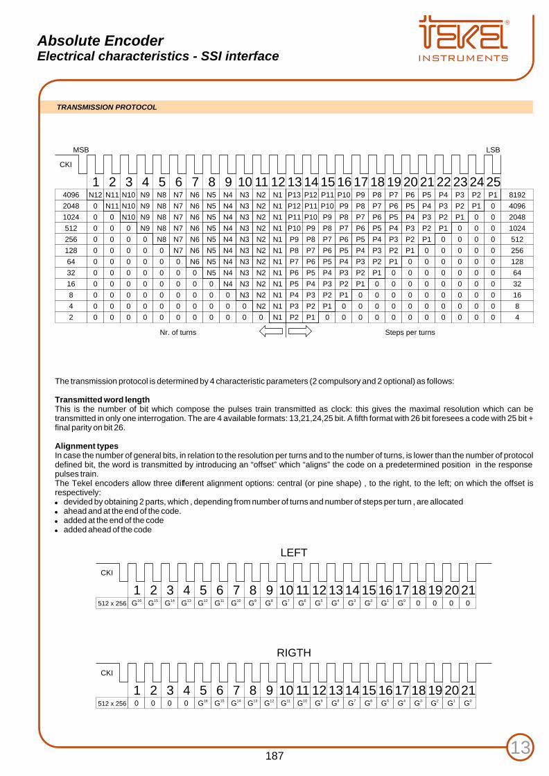
The transmission protocol is determined by 4 characteristic parameters (2 compulsory and 2 optional) as follows:
Transmitted word lengthThis is the number of bit which compose the pulses train transmitted as clock: this gives the maximal resolution which can be transmitted in only one interrogation. The are 4 available formats: 13,21,24,25 bit. A fifth format with 26 bit foresees a code with 25 bit + final parity on bit 26.
Alignment typesIn case the number of general bits, in relation to the resolution per turns and to the number of turns, is lower than the number of protocol defined bit, the word is transmitted by introducing an “offset” which “aligns” the code on a predetermined position in the response pulses train.The Tekel encoders allow three different alignment options: central (or pine shape) , to the right, to the left; on which the offset is respectively:! devided by obtaining 2 parts, which , depending from number of turns and number of steps per turn , are allocated! ahead and at the end of the code.! added at the end of the code! added ahead of the code
13
Absolute EncoderElectrical characteristics - SSI interface
187

Parity check (optional)One of the simplest and most common methods to identify errors in a package of data interchanged between two devices (for example encoder and controls system) consist in introducing 1 adding bit at the end of the code which identifies the parity:! in case of parity “ODD” (O) this bit has value 1 if the sum of the bit at “1” in the code, excluded the parity bit, is even; the value is “0” in
case the number of bit at “1” is odd.! in case of parity “.EVEN” this bit has value 1 if the sum of the bit at “1” in the code, excluded the parity bit, is odd; the value is “0” in case
the number of bit at “1” is even.
Up/Down (optional)We remind that the Tekel encoders are designed in order to:! increment counting when shaft rotates clockwise.! decrement counting when shaft rotates counter clockwise.The control of theUp/Down signal allows the invert the functioning logic with consequent decrement of signal when shaft rotates clockwise or vice versa. The activation of input Up/Down has consequence on the transmitted code with a certain delay which is defined TU/D time.
Gray Binary conversionA useful characteristic of serial data transmission, through SSI, consists in the extremely easy conversion of the data from Gray to Binary format. Only 2 components are sufficient: a port EXCLUSIVE-OR and a FLIP-FLOP.
1 2 3 4 5 6 7 8 9 10 11 12 13 14 15 16 17 18 19 20 21
CKI
DATA
DATA WORD
PARITYODD
H
DATAOUT
UP/DOWN
normal
GRAYBINARY
CKICLEAR
CLOCK
P/S
T U/D reverse
L
APPLICATION NOTES
14
Absolute EncoderElectrical characteristics - SSI interface
188

MS 26 P
S26 - SL26CONNECTOR
PIN
A
B
C
D
b
PIN
E
F
G
H
c
PIN
J
K
L
M
PIN
N
P
R
S
PIN
T
U
V
W
PIN
X
Y
Z
a
SIGN
02
122
232
N.C.
SIGN
42
52
62
72
N.C.
SIGN
82
92
VOID
MSB*
SIGN
MSB*
VOID
ZERO
VOID
SIGN
VOID
VOID
VOID
U/D
SIGN
VOID
+ Vcc
0 Volt
VOID
A
B
C
D
E
F
G
H
J
K
R
M
W
N
Y
Z
0G1G2G3G4G5G6G7G8G9G
ZERO
MSB*
U/D
MSB*
+ Vcc
0 Volt
02122232425262728292
ZERO
MSB*
U/D
MSB*
+ Vcc
0 Volt
2
15
3
16
4
17
5
18
6
19
22
13
10
14
25
1
WHT
PNK
BLU
YLW
GRN
BRW
GRY
VLT
WHT/BLK
WHT/RED
GRY/BRW
RED/BLU
WHT/GRN
WHT/YLW
RED
BLK
WHT
PNK
BLU
YLW
GRN
BRW
GRY
VLT
WHT/BLK
WHT/RED
GRY/BRW
RED/BLU
WHT/GRN
WHT/YLW
RED
BLK
1
6
7
4
3
2
5
10
25
23
18
12
13
15
8
9
white
pink
blue
yellow
green
brown
grey
violet
white and black
white and red
grey and brown
red and blue
white and green
white and yellow
red
black
=
=
=
=
=
=
=
=
=
=
=
=
=
=
=
=
D 25 P
D25CONNECTOR
CABLECOLOUR
GRAYsignals
BINARY signals
LEGENDA: Because of the small spaceon the label we had to abbreviate cable colours as follows
The relative number of the cable colour code meets DIN 47100 requirements.
* JUMPERS ( to program the up-down counts related to CW or CCW rotation of shaft)-MSB and U/D for CW rotation counting UP-MSB and U/D for CCW rotation counting UP
CONNECTOR MS3112A 16-26 otherwise called MS 26 P
ORDER CODE S26 o SL26 ORDER CODE D25
CONNECTION DIAGRAM FOR TKE 615 WITH SYNCHROTEK® INTERFACE
CONNECTOR D 25P
Y = + Vcc
Z = 0 Volt
* Jumper: pin U/D and 0 Volt for CCW rotation
CKI/CKI INVERTED = INPUT CLOCK LINEOUT/OUT INVERTED = OUTPUT DATA LINE
15
CONNECTIONS - Absolute encoders TKE series(for BCD code connections please sea TKC models)
AB
C
D
E
F
GHJ
K
L
M
N
PR
S T
U
V
WX
Y
Z
ab
c
GRAY
BINARY
1
2
3
4
5
6
7
8
9
10
11
12
13
14
15
16
17
18
19
20
21
22
23
24
25
0-Volt
02
22
42
62
82
0G
2G
4G
6G
8G
U/D
MSB*
MSB*
12
32
52
72
92
1G
3G
5G
7G
9G
Zero
+ Vcc
189
Green
Yellow
Brown
Red
Pink
Black
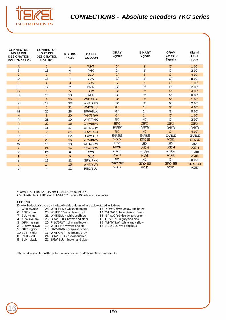
CONNECTIONS - Absolute encoders TKC series
CONNECTORMS 26 PIN
DESIGNATIONCod. S26 o SL26
A
B
C
D
E
F
G
H
J
K
L
M
N
P
R
S
T
U
V
W
X
Y
Z
a
b
c
0G1G2G3G4G5G6G7G8G9G
10G11G12G
NC
ZERO
PARITY
NC
ENABLE
VOID
U/D*
LATCH
+ Vcc
0 Volt
NC
ZERO SET
VOID
0G1G2G3G0G1G2G3G0G1G2G3G0G1G
ZERO
PARITY2G
ENABLE
VOID
U/D*
LATCH
+ Vcc
0 Volt3G
ZERO SET
VOID
01.1002.1004.1008.1011.1012.1014.1018.1021.1022.1024.1028.1031.1032.10
ZERO
PARITY34.10
ENABLE
STROBE
U/D*
LATCH
+ Vcc
0 Volt38.10
ZERO SET
VOID
02122232425262728292
102112122
NC
ZERO
PARITY
NC
ENABLE
STROBE
U/D*
LATCH
+ Vcc
0 Volt
NC
ZERO SET
VOID
2
15
3
16
4
17
5
18
6
19
7
20
8
21
22
11
9
12
23
10
24
25
1
13
14
--
1
6
7
4
3
2
5
10
25
23
21
26
20
19
18
17
24
22
16
13
14
8
9
11
15
12
WHT
PNK
BLU
YLW
GRN
BRW
GRY
VLT
WHT/BLK
WHT/RED
WHT/BLU
BRW/BLK
PNK/BRW
WHT/PNK
GRY/BRW
WHT/GRY
BRW/RED
BRW/BLU
YLW/BRW
WHT/GRN
BRW/GRN
RED
BLK
GRY/PNK
WHT/YLW
RED/BLU
CONNECTORD 25 PIN
DESIGNATIONCod. D25
CABLE COLOUR
RIF. DIN47100
GRAY Signals
GRAY Excess 3*
Signals
SignalBCDcode
BINARY Signals
* CW SHAFT ROTATION and LEVEL “1” = count UPCW SHAFT ROTATION and LEVEL “0” = count DOWN and vice versa
LEGENDDue to the lack of space on the label cable colours where abbreviated as follows:1 WHT =white 25 WHT/BLK = white and black 16 YLW/BRW = yellow and brown6 PNK = pink 23 WHT/RED = white and red 13 WHT/GRN = white and green7 BLU =blue 21 WHT/BLU = white and blue 14 BRW/GRN =brown and green4 YLW =yellow 26 BRW/BLK = brown and black 11 GRY/PNK = grey and pink3 GRN = green 20 PNK/BRW = pink and brown 15 WHT/YLW =white and yellow2 BRW = brown 19 WHT/PNK = white and pink 12 RED/BLU =red and blue5 GRY = grey 18 GRY/BRW = grey and brown10 VLT = violet 17 WHT/GRY = white and grey8 RED =red 24 BRW/RED = brown and red9 BLK =black 22 BRW/BLU = brown and blue
The relative number of the cable colour code meets DIN 47100 requirements.
16190

CONNECTOR MS3112A 16-26P otherwise called MS 26P
ORDER CODE S26 o SL26
S26 o SL26
ORDER CODE D25
CONNECTION DIAGRAM FOR SSI INTERFACE
CONNECTOR D 25 P
A
B
C
D
E
F
G
H
J
K
L
M
N
P
R
S
T
U
V
W
X
Y
Z
a
b
c
0 0G /21 1
G /22 2
G /23 3
G /24 4
G /25 5
G /26 6
G /27 7
G /28 8G /29 9G /210 10G /211 11G /212 12G /2
N.C.
ZERO SIGNAL
PARITY
VOID
ENABLE (3-STATE)
STROBE
U/D
LATCH
+ Vcc
0 Volt
VOID
VOID
VOID
0 0G /1.101 0
G /2.102 0G /4.103 0
G /8.100 1G /1.101 1G /2.102 1
G /4.103 1G /8.100 2
G /1.101 2G /2.102 2
G /4.103 2G /8.100 3
G /1.101 3G /2.10
ZERO SIGNAL
PARITY2 3
G /4.10
ENABLE (3-STATE)
STROBE
U/D
LATCH
+ Vcc
0 Volt
VOID
VOID
VOID
A
B
C
D
E
F
G
H
J
K
L
M
N
P
R
S
T
U
V
W
X
Y
Z
a
b
c
GRAY AND BINARY GRAY EXCESS 3 and BCD
PIN SIGNAL PIN SIGNAL
Y = + Vcc
Z = 0 Volt
7 pins connector MS3106A 16A 16S-1P
* For CCW rotation: Jump pin U/D and 0 Volt
CKI/CKI INVERTED = INPUT CLOCK LINEOUT/OUT INVERTED= OUTPUT CLOCK LINE
Issue 09/1999
CONNECTIONS - Absolute encoders TKC series
17191
AB
C
D
E
F
GHJ
K
L
M
N
PR
S T
U
V
WX
Y
Z
ab
c
Green
Yellow
Brown
Red
Pink
Black

For TKM60P (programmable version)
12 pins connector - Ordering code S12 o SL12
12 pin connector - Ordering code S12 o SL12
For TKC - TKM (not programmable versions)
1
2
3
4
5
6
7
8
9
10
11
12
0 Volt
Data +
CKI +
Rx +
Rx -
Tx +
Tx -
+ Vcc
Zero set
Data -
CKI -
Up/Down
PIN SIGNAL
Connections for 12 pins connector
Metal connectorshield on housing
1
2
3
4
5
6
7
8
9
10
11
12
0 Volt
Data +
CKI +
n.c.
n.c.
n.c.
n.c.
+ Vcc
Zero set
Data -
CKI -
Up/Down
PIN SIGNAL
Connections - Absolute encoders TKC - TKM series
18
] RS 432 RS 485 programming serial interface.For RS 232 connect only Tx+ and Rx+
192
Connections for 12 pins connector
Metal connectorshield on housing
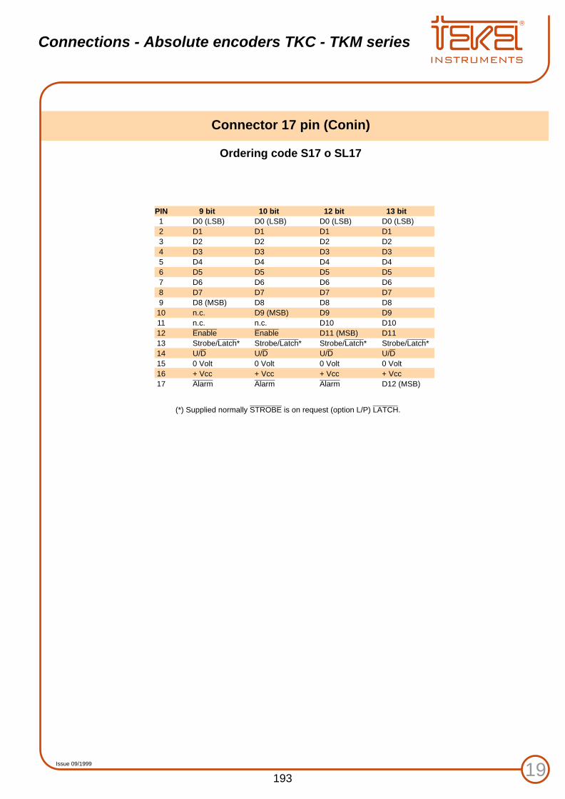
Connector 17 pin (Conin)
1
2
3
4
5
6
7
8
9
10
11
12
13
14
15
16
17
(*) Supplied normally STROBE is on request (option L/P) LATCH.
D0 (LSB)
D1
D2
D3
D4
D5
D6
D7
D8 (MSB)
n.c.
n.c.
Enable
Strobe/Latch*
U/D
0 Volt
+ Vcc
Alarm
D0 (LSB)
D1
D2
D3
D4
D5
D6
D7
D8
D9 (MSB)
n.c.
Enable
Strobe/Latch*
U/D
0 Volt
+ Vcc
Alarm
D0 (LSB)
D1
D2
D3
D4
D5
D6
D7
D8
D9
D10
D11 (MSB)
Strobe/Latch*
U/D
0 Volt
+ Vcc
Alarm
D0 (LSB)
D1
D2
D3
D4
D5
D6
D7
D8
D9
D10
D11
Strobe/Latch*
U/D
0 Volt
+ Vcc
D12 (MSB)
PIN 9 bit 10 bit 12 bit 13 bit
Connections - Absolute encoders TKC - TKM series
19Issue 09/1999
Ordering code S17 o SL17
193
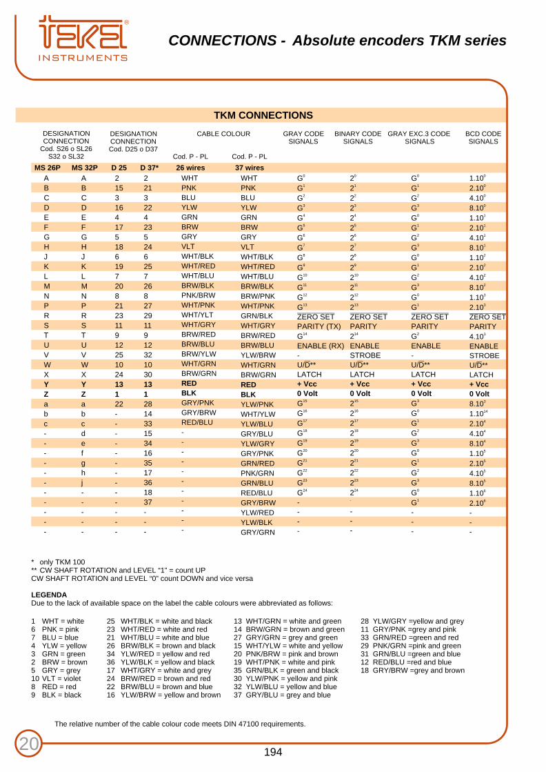
TKM CONNECTIONS
0G1
G2G3G0
G1
G2G3G0
G1
G2G3G0
G1
G
ZERO SET
PARITY2
G
ENABLE
-
U/D**
LATCH
+ Vcc
0 Volt3G0
G1
G2G3G0
G1
G2G3G0
G1G
-
-
-
0G1
G2G3G4
G5
G6G7G8
G9
G10G11G12
G13
G
ZERO SET
PARITY (TX)14
G
ENABLE (RX)
-
U/D**
LATCH
+ Vcc
0 Volt15G16
G17
G18G19G20
G21
G22G23G24
G
-
-
-
-
021
222324
25
262728
29
210211212
213
2
ZERO SET
PARITY14
2
ENABLE
STROBE
U/D**
LATCH
+ Vcc
0 Volt15216
217
218219220
221
222223224
2-
-
-
-
01.1002.1004.1008.1011.1012.1014.1018.1021.1022.1024.1028.1031.1032.10
ZERO SET
PARITY34.10
ENABLE
STROBE
U/D**
LATCH
+ Vcc
0 Volt38.10141.1042.1044.1048.1051.1052.1054.1058.1061.1062.10
-
-
-
DESIGNATIONCONNECTION
Cod. S26 o SL26S32 o SL32
MS 26P
A
B
C
D
E
F
G
H
J
K
L
M
N
P
R
S
T
U
V
W
X
Y
Z
a
b
c
-
-
-
-
-
-
-
-
-
-
-
A
B
C
D
E
F
G
H
J
K
L
M
N
P
R
S
T
U
V
W
X
Y
Z
a
b
c
d
e
f
g
h
j
-
-
-
-
-
MS 32P
DESIGNATIONCONNECTIONCod. D25 o D37
2
15
3
16
4
17
5
18
6
19
7
20
8
21
23
11
9
12
25
10
24
13
1
22
-
-
-
-
-
-
-
-
-
-
-
-
-
D 25
2
21
3
22
4
23
5
24
6
25
7
26
8
27
29
11
9
12
32
10
30
13
1
28
14
33
15
34
16
35
17
36
18
37
-
-
-
D 37*
WHT
PNK
BLU
YLW
GRN
BRW
GRY
VLT
WHT/BLK
WHT/RED
WHT/BLU
BRW/BLK
PNK/BRW
WHT/PNK
WHT/YLT
WHT/GRY
BRW/RED
BRW/BLU
BRW/YLW
WHT/GRN
BRW/GRN
RED
BLK
GRY/PNK
GRY/BRW
RED/BLU
-
-
-
-
-
-
-
-
-
-
-
26 wires
WHT
PNK
BLU
YLW
GRN
BRW
GRY
VLT
WHT/BLK
WHT/RED
WHT/BLU
BRW/BLK
BRW/PNK
WHT/PNK
GRN/BLK
WHT/GRY
BRW/RED
BRW/BLU
YLW/BRW
WHT/GRN
BRW/GRN
RED
BLK
YLW/PNK
WHT/YLW
YLW/BLU
GRY/BLU
YLW/GRY
GRY/PNK
GRN/RED
PNK/GRN
GRN/BLU
RED/BLU
GRY/BRW
YLW/RED
YLW/BLK
GRY/GRN
37 wires
CABLE COLOUR
Cod. P - PL Cod. P - PL
GRAY CODE SIGNALS
BINARY CODE SIGNALS
GRAY EXC.3 CODE SIGNALS
BCD CODE SIGNALS
* only TKM 100** CW SHAFT ROTATION and LEVEL “1” = count UPCW SHAFT ROTATION and LEVEL “0” count DOWN and vice versa
LEGENDADue to the lack of available space on the label the cable colours were abbreviated as follows:
1 WHT = white 25 WHT/BLK = white and black 13 WHT/GRN = white and green 28 YLW/GRY =yellow and grey6 PNK = pink 23 WHT/RED = white and red 14 BRW/GRN = brown and green 11 GRY/PNK =grey and pink7 BLU = blue 21 WHT/BLU = white and blue 27 GRY/GRN = grey and green 33 GRN/RED =green and red4 YLW = yellow 26 BRW/BLK = brown and black 15 WHT/YLW = white and yellow 29 PNK/GRN =pink and green3 GRN = green 34 YLW/RED = yellow and red 20 PNK/BRW = pink and brown 31 GRN/BLU =green and blue2 BRW = brown 36 YLW/BLK = yellow and black 19 WHT/PNK = white and pink 12 RED/BLU =red and blue5 GRY = grey 17 WHT/GRY = white and grey 35 GRN/BLK = green and black 18 GRY/BRW =grey and brown10 VLT = violet 24 BRW/RED = brown and red 30 YLW/PNK = yellow and pink8 RED = red 22 BRW/BLU = brown and blue 32 YLW/BLU = yellow and blue9 BLK = black 16 YLW/BRW = yellow and brown 37 GRY/BLU = grey and blue
CONNECTIONS - Absolute encoders TKM series
20
The relative number of the cable colour code meets DIN 47100 requirements.
194

21Issue 09/1999
CONNECTIONS - Absolute encoders TKC series
A
B
C
D
E
F
G
H
J
K
L
M
N
P
R
S
T
U
V
W
X
Y
Z
a
b
c
d
e
f
g
h
j
0 0G /2
1 1G /22 2
G /23 3G /24 4
G /25 5G /26 6
G /27 7G /28 8
G /29 9G /210 10G /211 11
G /212 12G /213 13
G /2
ZERO SET
PARITY14 14G /2
ENABLE
STROBE
U/D
LATCH
+ Vcc
0 Volt15 15G /216 16
G /217 17G /218 18
G /219 19G /220 20
G /221 21G /222 22
G /223 23G /2
0 0G /1.10
1 0G /2.102 0
G /4.103 0G /8.100 1
G /1.101 1G /2.102 1
G /4.103 1G /8.100 2
G /1.101 2G /2.102 2
G /4.103 2G /8.100 3
G /1.101 3G /2.10
ZERO SET
PARITY2 3
G /4.10
ENABLE
STROBE
U/D
LATCH
+ Vcc
0 Volt3 3
G /8.100 4G /1.101 4
G /2.102 4G /4.103 4
G /8.100 5G /1.101 5
G /2.102 5G /4.103 5
G /8.10
A
B
C
D
E
F
G
H
J
K
L
M
N
P
R
S
T
U
V
W
X
Y
Z
a
b
c
d
e
f
g
h
j
S26-SL26 limit
GRAY BINARY GRAY EXCESS 3 BCD
PIN SIGNAL PIN SIGNAL
MS3112A 16-26P connector - order code S26 - Sl26MS3112A 18-32P connector - order code S32 - Sl32
D25 P connector - order code D25D37 P connector - order code D37 (*)
S26-SL26
Y = + Vcc Z = 0 Volt
S32-SL32
(*) TKM100Only for
13 = + Vcc1 = + 0 Volt
AB
C
D
E
F
GHJ
K
L
M
N
PR
S T
U
V
WX
Y
Z
ab
c
AB
C
D
E
F
GHJ
K
L
M
N
PR
S T
U
V
WX
Y
Z
ab
c
195
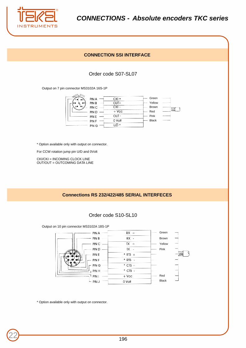
CONNECTIONS - Absolute encoders TKC series
22
CONNECTION SSI INTERFACE
Order code S07-SL07
Order code S10-SL10
* Option available only with output on connector.
For CCW rotation jump pin U/D and 0Volt
CKI/CKI = INCOMING CLOCK LINEOUT/OUT = OUTCOMING DATA LINE
Connections RS 232/422/485 SERIAL INTERFECES
* Option available only with output on connector.
196
Output on 7 pin connector MS3102A 16S-1P
Output on 10 pin connector MS3102A 18S-1P
Green
Green
Yellow
Yellow
Brown
Brown
Red
Red
Pink
Pink
Black
Black

23Issue 09/1999
GRAY CODE OUTPUT “NPN” AND “PNP”Absolute encoders
Step0
1
2
3
4
5
6
7
8
9
10
11
12
13
14
15
16
17
18
19
20
21
22
23
24
25
26
27
28
29
30
H
L
H
L
H
L
H
L
H
L
H
L
H
L
H
L
H
L
H
L
0G
1G
2G
3G
4G
0G
1G
2G
3G
4G
NPN OUTPUT (NEGATIVE LOGIC)
PNP OUTPUT (POSITIVE LOGIC)
Fig. 19
Fig. 20
197

24
UP/DOWN SELECTION (U/D)Operating characteristics of up/down - input signal
CW SHAFT ROTATION (Figs. 19 and 20)Standard version: if the signal is “HIGH” on U/D pin, the code counts “UP”;
if the signal is “LOW” on U/D pin, the code counts “DOWN”.
CCW SHAFT ROTATION (Figs. 19 and 20)Standard version: if the signal is “HIGH” on U/D pin, the code counts “DOWN”;
if the signal is “LOW” on U/D pin, the code counts “UP”.
If the inverted U/D active signal is desired, it is possible, on demand, to change the encoder program.
Shaft rotation*Output encoder
S i g n a l U / D
Shaft rotation*Output encoder
Signal U/D
Fig. 21*Shaft rotation as viewed from front shaft encoder
AVAILABLE FUNCTIONSAbsolute encoders
198
AVAILABLE FUNCTIONS
25Issue 09/1999
AVAILABLE FUNCTIONSAbsolute encoders
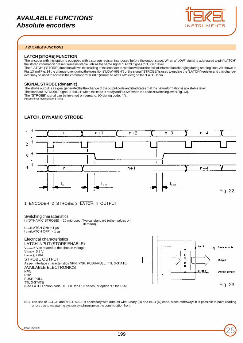
LATCH (STORE) FUNCTIONThe encoder with this option is equipped with a storage register interposed before the output stage. When a “LOW” signal is addressed to pin “LATCH” the stored information present remains stable until as the same signal “LATCH” goes to “HIGH” level. The “LATCH” (“STORE”) function allows the reading of the encoder in rotation without the risk of information changing during reading time. As shown in Fig. 13 and Fig. 14 the change-over during the transition (“LOW-HIGH”) of the signal “STROBE” is used to update the “LATCH” register and this change-over may be used to address the command “STORE” (it must be at “LOW” level) on the “LATCH” pin.
SIGNAL STROBE (dynamic)The strobe output is a signal generated by the change of the output code and it indicates that the new information is at a stable level. The standard “STROBE” signal is “HIGH” when the code is ready and “LOW” when the code is switching over (Fig. 13).The “STROBE” signal can be inverted on demand. (Ordering code: “I”).(*) Sometimes identified with STORE
N.B. The use of LATCH and/or STROBE is necessary with outputs with Binary (B) and BCD (D) code, since otherways it is possible to have reading errors due to measuring system synchronism on the commutation front.
Switching characteristicst s (DYNAMIC STROBE) = 20 microsec. Typical standard (other values on
demand).t L on (LATCH ON) > 1 µst L off (LATCH OFF) > 1 µs
Electrical characteristicsLATCH INPUT (STORE ENABLE)V I HIGH = Vcc related to the chosen voltageV I LOW < 0,7 VI I HIGH > 7 mA
STROBE OUTPUTAs per interface characteristics NPN, PNP, PUSH-PULL, TTL 3-STATE
AVAILABLE ELECTRONICSNPNPNPPUSH-PULLTTL 3-STATE(See LATCH option code 50…80 for TKC series, or option “L” for TKM
LATCH, DYNAMIC STROBE
1=ENCODER; 2=STROBE; 3=LATCH; 4=OUTPUT
Fig. 22
Fig. 23
199

26
PARITY SIGNAL (electronic)
The “PARITY” is a control signal used for the reading interface and it is used to verify that the information does not contain errors.The signal “PARITY” is “HIGH” when the Bits that make up the code, in encoder output, are even (Fig.15).A failure of the interface generates an error.PARITY output can be:
EVEN, standard version, code “E”ODD, optional version, code “O”
Fig. 24
Bit number at Highlogic level
Odd parity
Odd parity
ERROR
Fig. 25
AVAILABLE FUNCTIONSAbsolute encoders
200
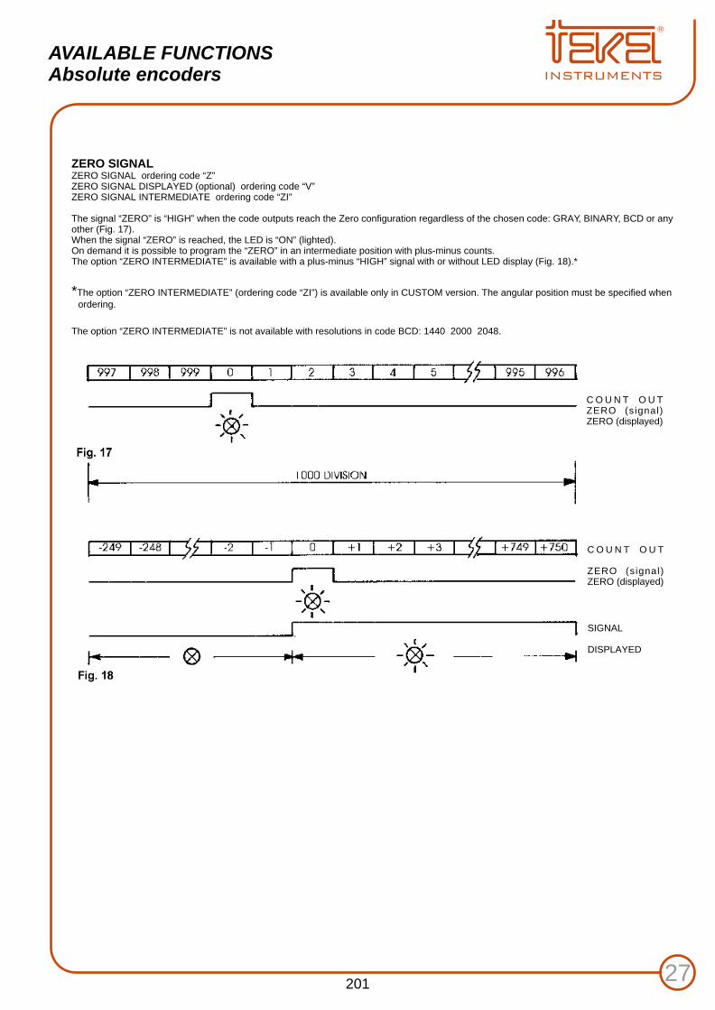
27
ZERO SIGNALZERO SIGNAL ordering code “Z”ZERO SIGNAL DISPLAYED (optional) ordering code “V”ZERO SIGNAL INTERMEDIATE ordering code “ZI”
The signal “ZERO” is “HIGH” when the code outputs reach the Zero configuration regardless of the chosen code: GRAY, BINARY, BCD or any other (Fig. 17).When the signal “ZERO” is reached, the LED is “ON” (lighted).On demand it is possible to program the “ZERO” in an intermediate position with plus-minus counts.The option “ZERO INTERMEDIATE” is available with a plus-minus “HIGH” signal with or without LED display (Fig. 18).*
*The option “ZERO INTERMEDIATE” (ordering code “ZI”) is available only in CUSTOM version. The angular position must be specified when ordering.
The option “ZERO INTERMEDIATE” is not available with resolutions in code BCD: 1440 2000 2048.
C O U N T O U TZERO (signal)ZERO (displayed)
C O U N T O U T
ZERO (signal)ZERO (displayed)
SIGNAL
DISPLAYED
AVAILABLE FUNCTIONSAbsolute encoders
201

28
AVAILABLE FUNCTIONSAbsolute encoders
Automatic zero or “Preset”
During the setting of the machinery it may be necessary to set the “zero machine” with the “zero encoder”. This operation can be carried out in two ways:a) turning the shaft of the encoder until the zero signal is found;b) using the “AUTOMATIC ZERO” option.
NORMAL COUNTINGWhen the multi-turn encoder is equipped with “AUTOMATIC ZERO” option, in normal counting conditions it is necessary that a voltage +Vdc is present on the pin or on the wire used for this option (for example, if the operative voltage is +5Vdc, the voltage present on the pin or on the wire used for the “AUTOMATIC ZERO” option must be +5Vdc, if the operative voltage is 11-30Vdc, the voltage must range between11-30Vdc). The current available must be 7 mA minimum, 15 mA maximum.
ZERO SETTING PROCEDUREDuring the normal counting condition it may be necessary to set the zero machine. In this case the encoder may be in any counting position (for example 16780).In order to obtain the automatic zero setting of the encoder counting this procedure must be followed:- convert the voltage of the pin or of the wire used for the “AUTOMATIC ZERO” option from +Vdc to 0 Volt. This condition must remained unchanged for at least 1mSec.- reconvert the voltage from 0 Volt to +Vdc. Automatically the previous counting position (for example 16780) becomes zero.
NN Code ZERO Code
tz
tz > 1 mstr = depends from encoder model and code type
tr
202