
Antenna Design Note - Quectel Wireless Solutions · Antenna Design Note Antenna_Design_Note...
22
Antenna Design Note Rev. Antenna_Design_Note_V1.8 Date: 2016-06-01 www.quectel.com
Transcript of Antenna Design Note - Quectel Wireless Solutions · Antenna Design Note Antenna_Design_Note...

Antenna Design Note
Rev. Antenna_Design_Note_V1.8
Date: 2016-06-01
www.quectel.com

Antenna Design Note
Antenna_Design_Note Confidential / Released 1 / 21
Our aim is to provide customers with timely and comprehensive service. For any
assistance, please contact our company headquarters:
Quectel Wireless Solutions Co., Ltd.
Office 501, Building 13, No.99, Tianzhou Road, Shanghai, China, 200233
Tel: +86 21 5108 6236
Email: [email protected]
Or our local office. For more information, please visit:
http://www.quectel.com/support/salesupport.aspx
For technical support, or to report documentation errors, please visit:
http://www.quectel.com/support/techsupport.aspx
Or email to: [email protected]
GENERAL NOTES
QUECTEL OFFERS THE INFORMATION AS A SERVICE TO ITS CUSTOMERS. THE INFORMATION
PROVIDED IS BASED UPON CUSTOMERS’ REQUIREMENTS. QUECTEL MAKES EVERY EFFORT
TO ENSURE THE QUALITY OF THE INFORMATION IT MAKES AVAILABLE. QUECTEL DOES NOT
MAKE ANY WARRANTY AS TO THE INFORMATION CONTAINED HEREIN, AND DOES NOT ACCEPT
ANY LIABILITY FOR ANY INJURY, LOSS OR DAMAGE OF ANY KIND INCURRED BY USE OF OR
RELIANCE UPON THE INFORMATION. THE INFORMATION SUPPLIED HEREIN IS SUBJECT TO
CHANGE WITHOUT PRIOR NOTICE.
COPYRIGHT
THE INFORMATION CONTAINED HERE IS PROPRIETARY TECHNICAL INFORMATION OF
QUECTEL CO., LTD. TRANSMITTING, REPRODUCTION, DISSEMINATION AND EDITING OF THIS
DOCUMENT AS WELL AS UTILIZATION OF THE CONTENT ARE FORBIDDEN WITHOUT
PERMISSION. OFFENDERS WILL BE HELD LIABLE FOR PAYMENT OF DAMAGES. ALL RIGHTS
ARE RESERVED IN THE EVENT OF A PATENT GRANT OR REGISTRATION OF A UTILITY MODEL
OR DESIGN.
Copyright © Quectel Wireless Solutions Co., Ltd. 2016. All rights reserved.
Quectel
Confidential

Antenna Design Note
Antenna_Design_Note Confidential / Released 2 / 21
About the Document
History
Revision Date Author Description
1.0 2012-06-09 David WEI Initial
1.1 2012-06-15 David WEI Modified Figure 1
1.2 2012-08-01 David WEI
Added contact information for antenna
manufacturers: Antenova and Pulse
Electronics
1.3 2012-11-21 David WEI Added contact information for GLONASS antenna
manufacturer INPAQ
1.4 2013-07-10 David WEI 1. Added ceramic chip antenna
2. Updated contact information
1.5 2014-11-21 Jackie WANG Added the antenna performance and LDS antenna
1.6 2015-04-11 Jackie WANG Added applicable modules
1.7 2016-01-06 Mark ZHANG
1. Added external PCB antenna
2. Added contact information for antenna
manufacturer SAINTENNA and JINGHONG
1.8 2016-06-01 Mark ZHANG
1. Updated the contact information of antenna
manufacturer JESONCOM
2. Updated the address and contact information
of antenna manufacturer Antenova
Quectel
Confidential

Antenna Design Note
Antenna_Design_Note Confidential / Released 3 / 21
Contents
About the Document ................................................................................................................................... 2
Contents ....................................................................................................................................................... 3
1 Recommended Component Placement of Main PCB ...................................................................... 4
2 Basic Parameters and Requirements of Antenna ............................................................................ 5
2.1. Basic Parameters of Antenna.................................................................................................... 5
2.2. Basic Requirements of Antenna ................................................................................................ 6
3 Embedded 2G/3G/4G Antenna ............................................................................................................ 7
3.1. PIFA Antenna with FPC Form ................................................................................................... 7
3.2. PIFA Antenna with Plastic Bracket ............................................................................................ 8
3.3. Monopole Antenna .................................................................................................................... 9
3.4. FPC Dipole Antenna ................................................................................................................ 10
3.5. PCB Antenna ........................................................................................................................... 11
3.6. Chip Antenna ........................................................................................................................... 12
3.7. Laser Direct Structure Antenna ............................................................................................... 13
4 External 2G/3G/4G Antenna .............................................................................................................. 14
4.1. Dipole Antenna ........................................................................................................................ 14
4.2. Monopole Antenna .................................................................................................................. 15
4.3. PCB Antenna ........................................................................................................................... 16
5 Embedded GPS Antenna................................................................................................................... 17
5.1. Example of Embedded GPS Antenna with RF Connector ..................................................... 17
5.2. Embedded GPS Patch Antenna with Welding Needle ........................................................... 18
6 External GPS Antenna ....................................................................................................................... 19
6.1. External GPS Antenna ............................................................................................................ 19
7 Antenna Suppliers Information ........................................................................................................ 20
Quectel
Confidential

Antenna Design Note
Antenna_Design_Note Confidential / Released 4 / 21
1 Recommended Component Placement
of Main PCB
This document is applicable to all Quectel modules.
Figure 1: Ideal Component Placement
Notes:
1. It is suggested to keep the RF ports on the outer side of PCB when displaying the module.
2. Put antenna pin at the edge of the main PCB, not in the center.
3. Keep antenna as far away from CPU\FLASH\DCDC\DISPLAY FPC as possible. It is preferred to
place the antenna in the different side of CPU\FLASH\DCDC\DISPLAY CONNECTOR.
4. Keep the high speed lines between CPU and DISPLAY as short as possible, put these lines in inner
layers and protect them with ground as well as possible. Add some EMI filters in the lines if
necessary
5. Put CPU\FLASH\DCDC\DISPLAY ZIF in shield case.
Quectel
Confidential
Antenna Design Note
Antenna_Design_Note Confidential / Released 5 / 21
2 Basic Parameters and Requirements
of Antenna
2.1. Basic Parameters of Antenna
Gain (dBi): The ratio of “power of antenna” and “power of isotropic radiation from an ideal current source”
in maximum transmitting direction with the same input power. “dBi” is widely used as the unit of antenna
gain.
Gain (dBd):
The ratio of “power of antenna” and “power of half wave dipole antenna” in maximum transmitting
direction with the same input power. One formula indicating relationship between dBi and dBd is given as
below:
dBi=2.15+dBd
Directivity: The ratio of “power of antenna” and “power of isotropic radiation from an ideal current source”
in maximum transmitting direction with the same radiated power.
Efficiency: The ratio of the antenna radiation power and antenna input power.
APIP (Antenna Port Input Power): The input power to antenna.
EIRP (Effective Isotropic Radiated Power): Compared to isotropic antenna, it is the power obtained in
maximum transmitting direction. Its formula is:
EIRP=P*G (Here P is radiation power, G is antenna gain indicated in dBi.)
PEIRP (Peak Effective Isotropic Radiated Power): The peak value of EIRP.
ERP (Effective Radiated Power): Comparing to half wave dipole antenna, it is the power obtained in
maximum transmitting direction. Its formula is:
EIRP=P*G (Here P is radiation power, G is antenna gain indicated in dBd.)
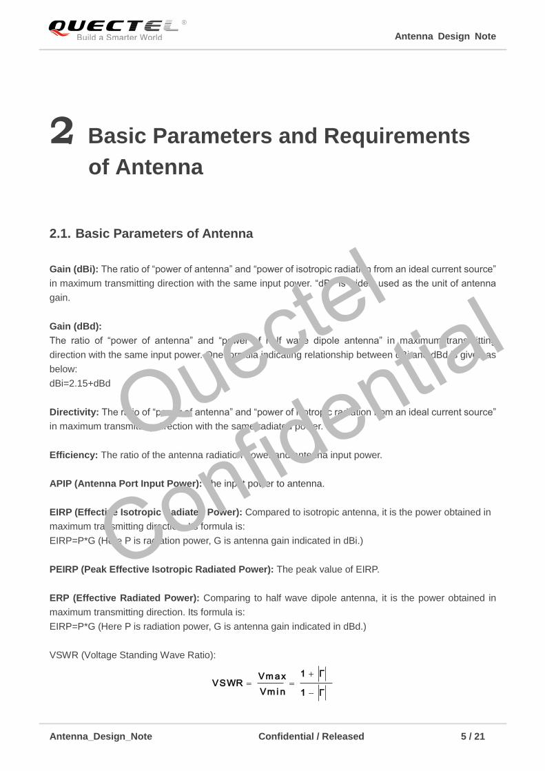
VSWR (Voltage Standing Wave Ratio):
Γ1
Γ1
Vm i n
VmaxVSWR
Quectel
Confidential
Antenna Design Note
Antenna_Design_Note Confidential / Released 6 / 21
Voltage standing wave ratio return loss is commonly used in engineering RL (S11), corresponding
relationship is shown as the following table:
)(dB1-V
1V20lgRLformula ingcorrespond The
:
VSWR(K) 1.20 1.25 1.30 1.35 1.40 1.50 2.00
Return loss (dB) -21.00 -19.00 -17.60 -16.60 -15.60 -14.00 -9.50
2.2. Basic Requirements of Antenna
Table 1: Basic Requirements of Antenna
Type Requirements
Frequency Range According to the operating band of device
VSWR ≤ 3
Gain (dBi) ≥1
Max Input Power (W) 50
Input Impedance (Ω) 50
Polarization Type
Vertical linear polarization (GSM/WCDMA CDMA2000
TD-SCDMA/LTE)
Right hand circular polarization (GPS)
Quectel
Confidential
Antenna Design Note
Antenna_Design_Note Confidential / Released 7 / 21
3 Embedded 2G/3G/4G Antenna
3.1. PIFA Antenna with FPC Form
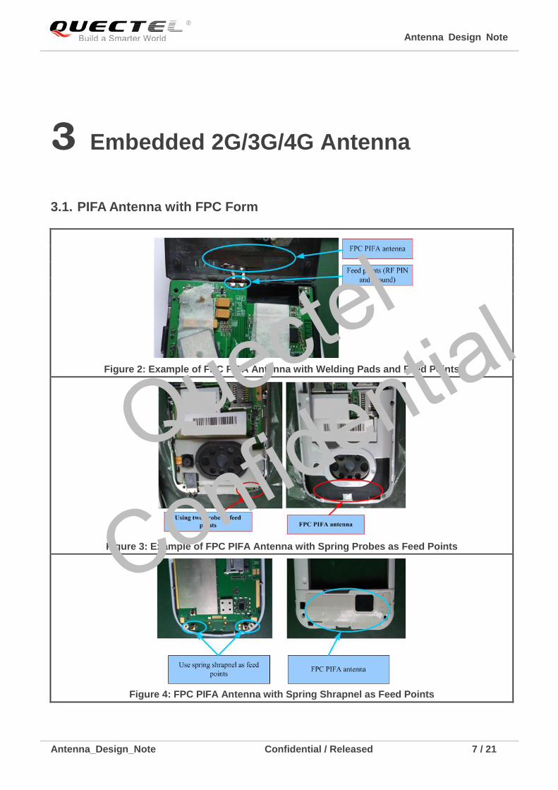
Figure 2: Example of FPC PIFA Antenna with Welding Pads and Feed Points
Figure 3: Example of FPC PIFA Antenna with Spring Probes as Feed Points
Figure 4: FPC PIFA Antenna with Spring Shrapnel as Feed Points
Quectel
Confidential
Antenna Design Note
Antenna_Design_Note Confidential / Released 8 / 21
Notes:
1. FPC PIFA antenna can be pasted in the casing, which can save space especially for PDA and
vehicle device.
2. Keep the distance between antenna and main PCB at least 5 millimeters.
3. Ground copper is required under antenna area in the main PCB.
4. Feed points can be designed as spring probes, shrapnel, welding pads. For more reliability, some
melted plastic leg can be designed inside the device casing.
3.2. PIFA Antenna with Plastic Bracket
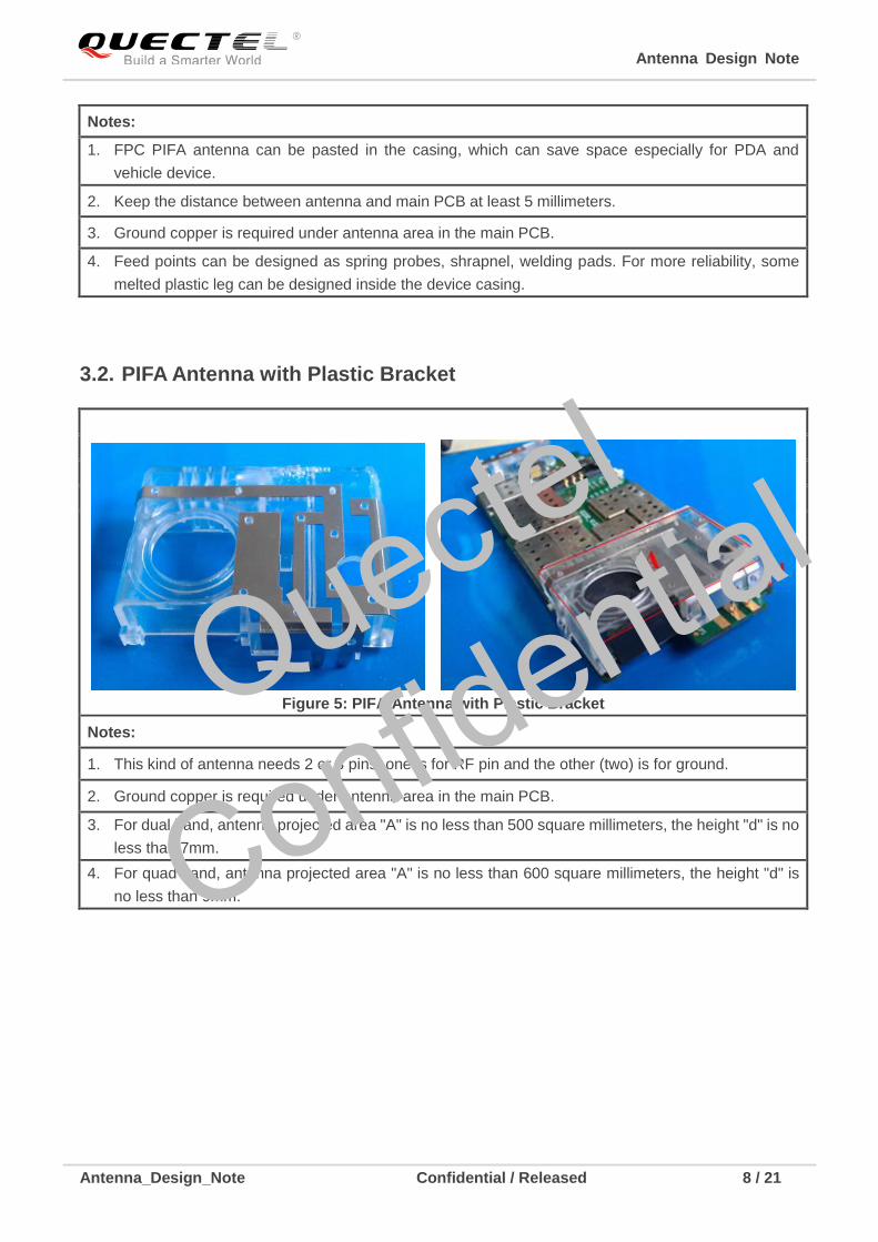
Figure 5: PIFA Antenna with Plastic Bracket
Notes:
1. This kind of antenna needs 2 or 3 pins, one is for RF pin and the other (two) is for ground.
2. Ground copper is required under antenna area in the main PCB.
3. For dual band, antenna projected area "A" is no less than 500 square millimeters, the height "d" is no
less than 7mm.
4. For quad band, antenna projected area "A" is no less than 600 square millimeters, the height "d" is
no less than 9mm.
Quectel
Confidential

Antenna Design Note
Antenna_Design_Note Confidential / Released 9 / 21
3.3. Monopole Antenna
Figure 6: Example of FPC Monopole Antenna
Figure 7: Example of FPC Monopole Antenna Pasted inside the Casing
Figure 8: Monopole Antenna with Plastic Bracket
Notes:
1. This kind of antenna only has one feed point.
2. A certain clearance area in all layers under antenna of host PCB is required.
3. For dual band antenna, the height of the bracket is more than 6mm and the clearance area in PCB
Quectel
Confidential

Antenna Design Note
Antenna_Design_Note Confidential / Released 10 / 21
should be more than 360 square millimeters. For quad band, the height and clearance area should
be 8mm and 400 square millimeters respectively.
3.4. FPC Dipole Antenna
Figure 9: Example of Dipole Antenna with FPC Form
Note:
The distance between inner edge of antenna and main PCB ground (marked as “d”) should be more
than 8 millimeters.
Quectel
Confidential

Antenna Design Note
Antenna_Design_Note Confidential / Released 11 / 21
3.5. PCB Antenna
Figure 10: Example of PCB Antenna
Figure 11: Example of Practical Applications of PCB Antenna
Notes:
1. This kind of antenna can be fixed to plastic box and does not need any host PCB area. It will be
better if the antenna is mounted in suitable notch.
2. There should be no metal material around antenna.
3. Antenna can be connected by RF connector or welding pad.
Quectel
Confidential

Antenna Design Note
Antenna_Design_Note Confidential / Released 12 / 21
3.6. Chip Antenna
Figure 12: Example of Ceramic Chip Antenna
Notes:
1. This kind of antenna needs enough main PCB size.
2. There should be no metal material under antenna.
3. This kind of antenna should be placed on the edge of main PCB and can be packaged in SMT type.
Quectel
Confidential

Antenna Design Note
Antenna_Design_Note Confidential / Released 13 / 21
3.7. Laser Direct Structure Antenna
Figure 13: Example of Laser Direct Structure Antenna
Notes:
1. The performance of the antenna is stable and has good consistency and high precision.
Manufacturing cycle is short. There is no need of circuit graphics mould. And it is the green product
as well.
2. The antenna is radiated on the mobile phone shell to prevent the interference of mobile phone
internal components, thus the signal is stable.
3. It is easier to make the device smaller and thinner.
4. The cost of LDS antenna is higher than common type because of the complex production process.
Quectel
Confidential

Antenna Design Note
Antenna_Design_Note Confidential / Released 14 / 21
4 External 2G/3G/4G Antenna
4.1. Dipole Antenna
Figure 14: Example of Dipole Antenna
Notes:
1. The height between antenna and main metal board "h" should be more than 8 centimeters.
2. The length of cable should be as short as possible. The shield copper wire net of the cable should be
as dense as possible. The quantity for surround copper lines used to shield signal should be no less
than 32.
Quectel
Confidential

Antenna Design Note
Antenna_Design_Note Confidential / Released 15 / 21
4.2. Monopole Antenna
Figure 15: Example of Practical Monopole Antennas
Notes:
1. There should be no other metal pole 200 millimeters around the antenna.
2. VSWR for stubby antenna should be less than 4, and VSWR for vehicle with long cable should be
less than 2.
3. The length of cable should be as short as possible. The quantity for surround copper lines used to
shield signal should be no less than 32.
Quectel
Confidential

Antenna Design Note
Antenna_Design_Note Confidential / Released 16 / 21
4.3. PCB Antenna
Figure 16: Example of PCB Antenna
Notes:
1. The performance of the external antenna is stable and superior.
3. Keep antenna perpendicular to the ground and avoid being surrounded by metal objects.
4. As two branches of LTE antenna, the main antenna is responsible for sending and receiving signals
and the diversity antenna is only responsible for receiving signals. Diversity antenna mainly resists
multipath fading and fast fading. Considering the receive gain of diversity antenna is much worse than
main antenna, the gain of diversity antenna should be controlled under 3dBi.
5. Attention should be paid to the relative position between main antenna and diversity antenna, the
overall performance would be better when isolation is less than 10dB between antennas in view of
distance and polarization isolation.
6. The multi-antenna technology (MIMO) has the ability to transmit high-speed data and resist
interference in the future.
Quectel
Confidential

Antenna Design Note
Antenna_Design_Note Confidential / Released 17 / 21
5 Embedded GPS Antenna
5.1. Example of Embedded GPS Antenna with RF Connector
Figure17: Example of Embedded GPS Antenna with RF Connector
Notes:
1. Keep antenna radiation side towards open sky during practical application.
2. Be sure the height of metal component nearby is lower than antenna radiation side.
3. Square shape is RHCP polarization, rectangle shape is linear polarization, and the former is
preferred.
4. Keep RF cable line as short as possible.
Quectel
Confidential

Antenna Design Note
Antenna_Design_Note Confidential / Released 18 / 21
5.2. Embedded GPS Patch Antenna with Welding Needle
Figure18: Example of Embedded GPS Patch Antenna with Welding Needle
Figure 19: Example of Practical Application of GPS Patch Antenna with Welding Needle
Notes:
1. Keep antenna radiation side towards open sky during practical application.
2. Be sure the height of metal component nearby is lower than antenna radiation side.
3. Square shape is RHCP polarization, rectangle shape is linear polarization, and the former is
preferred.
Quectel
Confidential

Antenna Design Note
Antenna_Design_Note Confidential / Released 19 / 21
6 External GPS Antenna
6.1. External GPS Antenna
Figure 20: Example of External GPS Antenna
Notes:
1. Keep antenna radiation side towards open sky during practical application.
2. Be sure the height of metal component nearby is lower than antenna radiation side.
3. Square shape is RHCP polarization, rectangle shape is linear polarization, and the former is
preferred.
4. Keep RF cable line as short as possible.
Quectel
Confidential

Antenna Design Note
Antenna_Design_Note Confidential / Released 20 / 21
7 Antenna Suppliers Information
Antenna
Manufacturer Address Contact Information Main Products
GSM Antenna Manufacturer
SAINTENNA
2nd Floor, 8th
Building,
No.611, Baoqi
Road, Baoshan
District,
Shanghai
Robin Yu
Fax +86-21-36307757 All kinds of embedded
and external antenna
which supports LTE,
WCDMA, EVDO, GSM
etc.
Mail robin.yu@saintenna
.com
Phone +86-21-36307732
+86-13817683329
JINGHONG
Room 501, 9th
Building,
No.518
XinZhuan
Road,
Caohejing
Development
Zone,
Shanghai,
China
Daniel
Ding
Fax +86-21-37632209
JINGHONG offers all
kinds of antennas
suited for GSM and
CDMA, 3G, 4G, LTE,
GPS and Wi-Fi.
Mail daniel.ding@wireles
s-sh.com
Phone +86-21-67766362
+86-13818493259
Web Http://www.jinghong
-sh.com
JESONCOM
No.358,
Liuyuan Road.,
Baoshan
District,
Shanghai,
China
Yuegang
Zhang
Phone +86-18101816628 All kinds of embedded
and external antenna
which supports
WCDMA, EVDO, GSM,
GPS/GLONASS etc.
Fax +86-21-66276923
Mail Alex.zhang@shjeso
ncom.com
Web www.shjesoncom.c
om
Antenova
2nd floor, Titan
Court, 3 Bishop
Square,
Hatfield, Herts
AL10 9NA,
United
Kingdom
Fax +44 (0) 1223
810650
Antenova’s broad
range of antennas and
RF solutions are ideally
suited for GSM and
CDMA, 3G, 4G, LTE,
GPS, Wi-Fi®,
Bluetooth®, WiMAX™,
WiBro, ZigBee®, FM,
Mobile TV and M2M
applications.
Phone +44 (0) 1223
810600
Mail sales@antenova-m
2m.com
Web http://www.antenova
-m2m.com
Quectel
Confidential
Antenna Design Note
Antenna_Design_Note Confidential / Released 21 / 21
Pulse
Electronics
European
Headquarters
Automotive
Headquarters
Zeppelinstrasse
15
71083
Herrenberg
Germany
Fax +49-7032-7806-12
Pulse Electronics is a
leading global supplier
of LTE; WLAN, 3G /
4G, Navigation, and
M2M fixed and mobile
solutions.
Phone +49-7032-7806-0
prodinfo.antennase
urope@pulseelectro
nics.com
Web http://www.pulseele
ctronics.com
GPS&GLONASS Antenna Manufacturer
INPAQ
No. 1800
Zhongshan
West Road, 4th
Floor, Zhao
Feng Universe
Building Block
D, Xuhui
District,
Shanghai,
China
Berry
Zhou
Mob. +86-18621809429
INPAQ offers all kinds
of GPS/GLONASS
antenna such as patch
antenna, active
antenna, chip antenna
and customized
antenna.
Phone +86-21-64400398*2
6812
Mail berryzhou@inpaqgp
.com
Web http://www.inpaq.co
m.tw
Note: If the salesmen listed above cannot be contacted for some reason, please visit their web
site and get the products and contact information.
Quectel
Confidential


