
Analysis of a Frequency Converter Equipped with Diode...
82
Analysis of a Frequency Converter Equipped with Diode Rectifier and Small DC Link Capacitor Institute of Energy Technology Master Thesis Conducted by Thordur Ofeigsson, spring 2008
Transcript of Analysis of a Frequency Converter Equipped with Diode...

Analysis of a Frequency Converter Equipped withDiode Rectifier and Small DC Link Capacitor
Institute of Energy Technology
Master Thesis
Conducted by Thordur Ofeigsson, spring 2008


Institute of Energy Technology
Pontoppidanstræde 101
Telephone 96 35 92 40
Fax 98 15 14 11
http://www.iet.aau.dk
Title:
Analysis of a frequency converterequipped with diode rectifier andsmall DC link capacitor
Project period:4. February - 4. June 2008
Project group number:PED10-1015a
Conducted by:Thordur Ofeigsson
Supervisor:Stig Munk-Nielsen
Number of copies: 6
Number of pages: 69
Finished: 4. June 2008
Abstract:
This project is focused on a low cost frequencyconverter equipped with diode rectifier andsmall DC link capacitor. The problems associ-ated with this configuration are the high fluc-tuations introduced in the DC link voltage.Due to the small capacitor the diode recti-fier harmonics are not rejected as the naturalfrequency of the DC link is above six timesthe grid side frequency. When this type of fre-quency converter is used to drive a squirrelcage induction motor the system is very sen-sitive to changes in speed. Quick changes inspeed cause large overvoltages in the DC linkvoltage which in turn could trigger the over-voltage protection of the frequency converter.Therefore the dynamics of the system are verypoor.The projects main goal is to analyse stabilitymargins of the frequency converter and exam-ine the influence of different parameters on thestability of the system. In order to analyse sta-bility a mathematical model of the system hasto be obtained. The model is then linearizedto derive transfer functions that describe theinfluence of different inputs on the DC linkvoltage. The stability analysis can then becarried out using conventional control theory.The obtained stability margins are then eval-uated with simulations in Matlab/Simulink.To fit with the topic of a low cost drive, a sen-sorless V/f control strategy is also designedand verified with simulations. The open loopV/f control and space vector modulation arethen implemented on a DSP to examine thesystem behavior in practice. Experimental re-sults were acquired and documented.

Preface
This project report entitled Analysis of a frequency converter equipped with diode rectifier and smallDC link capacitor is documented by group PED10-1015a on 10th semester at Institute of EnergyTechnology, Aalborg University.
Literature references are mentioned in square brackets by numbers which have their correspond-ing equivalent in the Bibliography with more detailed information about the literature. Appendicesare assigned with letters and are arranged in alphabetical order in the back of the report. Equationsare numbered in format (X.Y) and figures are numbered in format fig. X.Y, where X is the chapternumber and Y is the number of the item. The contents of the enclosed CD-ROM are explained inappendix D.
The author would like to thank Stig Munk-Nielsen for his supervision on the project and alsothe people at Danfoss, Radu Dan Lazar and Johnny Wahl Jensen, for their help and hardwaresupport.
The report is conducted by:
Thordur Ofeigsson
Contents
1 Introduction 21.1 Background . . . . . . . . . . . . . . . . . . . . . . . . . . . . . . . . . . . . . . . . . 21.2 Problem description . . . . . . . . . . . . . . . . . . . . . . . . . . . . . . . . . . . . 51.3 Project goals . . . . . . . . . . . . . . . . . . . . . . . . . . . . . . . . . . . . . . . . 61.4 Limitations . . . . . . . . . . . . . . . . . . . . . . . . . . . . . . . . . . . . . . . . . 6
2 Models and sensorless V/f control 72.1 Space Vector Modulation . . . . . . . . . . . . . . . . . . . . . . . . . . . . . . . . . 72.2 Time delay . . . . . . . . . . . . . . . . . . . . . . . . . . . . . . . . . . . . . . . . . 82.3 Voltage source inverter . . . . . . . . . . . . . . . . . . . . . . . . . . . . . . . . . . . 92.4 Induction motor . . . . . . . . . . . . . . . . . . . . . . . . . . . . . . . . . . . . . . 112.5 Sensorless V/f control . . . . . . . . . . . . . . . . . . . . . . . . . . . . . . . . . . . 162.6 Simulations . . . . . . . . . . . . . . . . . . . . . . . . . . . . . . . . . . . . . . . . . 212.7 Summary . . . . . . . . . . . . . . . . . . . . . . . . . . . . . . . . . . . . . . . . . . 28
3 Stability analysis and DC link dimensioning 293.1 Deriving the transfer functions . . . . . . . . . . . . . . . . . . . . . . . . . . . . . . 293.2 Stability analysis . . . . . . . . . . . . . . . . . . . . . . . . . . . . . . . . . . . . . . 353.3 Dimensioning the DC link capacitor . . . . . . . . . . . . . . . . . . . . . . . . . . . 403.4 Simulations . . . . . . . . . . . . . . . . . . . . . . . . . . . . . . . . . . . . . . . . . 413.5 Summary . . . . . . . . . . . . . . . . . . . . . . . . . . . . . . . . . . . . . . . . . . 53
4 Implementation 544.1 Test setup . . . . . . . . . . . . . . . . . . . . . . . . . . . . . . . . . . . . . . . . . . 544.2 Experimental results . . . . . . . . . . . . . . . . . . . . . . . . . . . . . . . . . . . . 584.3 Summary . . . . . . . . . . . . . . . . . . . . . . . . . . . . . . . . . . . . . . . . . . 63
5 Conclusion 64
6 Future work 66
A SVM S-function code 69
B Screenshots from oscilloscope 71
C Motor nameplates 77
D Contents of CD-ROM 78

Chapter 1
Introduction
This chapter gives description of the project and provides some relevant background information.Project goals and limitations are outlined as well.
1.1 Background
The frequency converter used within this project is shown in fig. 1.1. It is equipped with a dioderectifier on the grid side, DC link capacitor and an inverter on the motor side. Many other varietiesof the frequency converter exist but the focus is kept on the previously mentioned arrangementwhere it is the arrangement involved in this project.
Grid side Motor side
C
DC link Load
Rg Lg
Rg Lg
Rg Lg
vag
vbg
vcg
Grid
Figure 1.1: Frequency converter.
Rectifier-inverter topology
To begin with, the circuit in fig. 1.1 will be studied with no inductance involved, Lg = 0. If themotor side inverter is neglected, the DC link voltage is rather constant for large capacitance wherethe capacitor filters the diode rectifier harmonics effectively. Therefore, almost no current will flowthrough the capacitor due to the relationship:
iC = CdvCdt
(1.1)
where iC is the current through the capacitor, C is the capacitance and vC is the voltage over thecapacitor.
But if the capacitance is lowered, fluctuations in the DC link voltage, with 6 times the gridside frequency, increase. This is because the natural frequency of the DC link is increased and doestherefore not reject the rectifier harmonics as effectively. This can also be viewed from energy laws,where the energy injected through the diode rectifier is still the same. This can be seen from thefollowing relationship:
2

CHAPTER 1. INTRODUCTION
WC(t) =∫ t1
t0p(t)dt =
C
2
(v2C(t1)− v2
C(t0))
(1.2)
where WC(t) is the total energy injected to the capacitor and p(t) is the instant power through thecapacitor. Fig. 1.2 shows vC(t) as the capacitor charges or discharges, it is shown that WC(t) is thearea under the voltage curve as the capacitor is being charged.
Charging Discharging
t0 t1 t2
vc(t)
Wc(t)
t
Figure 1.2: Voltage over the capacitor when it charges and dishcarges.
As C is lowered the difference between the maximum and minimum value of vC has to increaseif the same energy is injected to the capacitor. And as the voltage fluctuations increase, the currentthrough the capacitor increases in order to fulfill (1.1).
But this arrangement introduces some problems with inrush currents and overvoltages at theinstance of grid connection. For a worst case situation when the DC link capacitor is fully dischargedand the grid side voltage is at its peak value the maximum theoretical voltage over the DC linkcapacitor would be 2
√2VLL, VLL being the line-to-line grid voltage, which could possibly destroy
the capacitor. Together with the overvoltage, a large inrush current would also occur. With noinductance involved the inrush current would rise very quickly to a high value. The inrush currentcould possibly destroy the diodes, the DC link capacitor or the load, [1].
Effects of inductance
In practice, a grid inductance Lg is always present on the grid side, as shown in fig. 1.3. The sizeof Lg can vary depending on whether the grid is stiff or weak.
Grid side Motor side
C
L
DC link Load
Rg Lg
Rg Lg
Rg Lg
vag
vbg
vcg
Grid
Figure 1.3: Frequency converter with DC choke.
Normally the DC link capacitor is large to provide a stable DC voltage, a small Lg then in-troduces a very high harmonic distortion and a low power factor. An optional inductance can beadded, either as a DC choke or an AC choke, depending if the optional inductance is located on
3

1.1. BACKGROUND
the DC or the AC side of the diode rectifier. The total inductance can then be increased which willdecrease the harmonic distortion and give larger power factor, [2].
Three phase inverter
The motor side converter is a three phase inverter, as shown in fig. 1.4.
ABC
Figure 1.4: Three phase inverter.
The three phase inverter consists of six switches parallely connected to diodes, to provide a re-turn path for the load current. The inverter utilizes the DC link voltage to the load in a controlledfashion using pulse width modulated gate signals. The preferred pulse width modulation methodsare the carrier-based methods because they provide low harmonic distortion and well defined har-monic spectrum. The carrier-based methods can mainly be implemented in two ways, using thetriangle intersection technique or the direct digital technique. The former technique compares asinusoidal control signal to a high frequency triangular wave to create the gate singals. The lattertechnique constructs the gate signals by precalculating the required time duration of each gatesignal pulse using space vector theory. Many methods exist for producing pulse width modulatedgate signals, the difference for carrier-based methods lies in the decision of the zero sequence sig-nal for the triangle intersection technique and in partioning of the zero states in the direct digitaltechnique, [3].
In practice, the switches do not switch states instantly, therefore the inverter is usually equippedwith deadtime that delays the turn-on and turn-off of every switch to prevent a short-circuit througheach inverter leg. The deadtime has several negative effects on the output voltage, like reducing thefundamental component and adding lower order harmonics, [4].
As the progress continues in power semiconductor devices, higher power ratings and switchingfrequencies become available for inverters. Many switching devices exist and the choice dependsmainly on current and voltage ratings and switching frequency. But other characteristics are alsoimportant, these are [1]:
• Small leakage current.
• Small on-state resistance.
• Small on-state voltage.
• Short turn-on and turn-off times.
• Large forward- and reverse-voltage blocking.
• High on-state current rating.
• Positive temperature coefficient of on-state resistance.
4

CHAPTER 1. INTRODUCTION
• Gate drive complexity.
• Tolerance of rated voltage and current during switching.
• Large dv/dt and di/dt ratings.
DC link capacitor
Because of its high capacitance per volume ratio, the electrolytic capacitor has been the preferredcapacitor for the DC link for years, where high capacitance gives smoother DC link voltage. Butthe electrolytic capacitor is expensive and heavy, and introduces considerable explosive risks andis usually the component that fails in the frequency converter, reducing the lifetime of the system,[5] [6]. Therefore researchers have been looking for a replacement for the electrolytic capacitor.But replacing the electrolytic capacitor would result in a DC link with lower capacitance whichdoes not provide as effective filtering of the rectifier harmonics. But, lower capacitance would alsoallow higher AC current to travel through the capacitor, reducing the line current harmonics, butalso increasing the stress on the capacitor and increasing the risk of capacitor breakdown. Due tothese reasons, the most promising substitude has been the metallized polypropylene film (MPPF)capacitor. Because of its very low losses, it permits a relatively higher AC current compared to othercapacitor types, decreasing the risk of breakdown, [7]. Also, the MPPF capacitor is lightweight, withmuch longer lifetime and no explosion risk compared to the electrolytic capacitor, [5] [7] [8] [9].
On the downside, the MPPF capacitor has much lower capacitance per volume ratio, the ca-pacitance being about 1% of the electrolytic capacitor for the same volume [6]. With lower DClink capacitance voltage fluctuations are increased. In normal induction motor drives, the motorcontrol attempts to keep the average power constant at constant speed, but with large voltagefluctuations the motor control causes the stator current to fluctuate. This can cause the drive tobecome unstable [10].
1.2 Problem description
The project proposal was given by Danfoss and deals with frequency converter consisting of adiode rectifier on the grid side, small DC link capacitor and full bridge inverter on the motor side.As the system layout shows in fig. 1.5 there is no DC choke present. Furthermore, there is nospeed measurement from the squirrel cage induction motor (SCIM) which consequently requires asensorless motor control. The SCIM is loaded with a DC motor which gives the ability to test thecontrol strategy for different loads. The controller will interact with the motor side inverter usingfeedback of measured currents and voltages from DC link and stator to calculate the duty cyclesfor the inverter.
The problem arises from the small DC link capacitor which causes large variations in the DClink voltage. The system has to be linearized to find stability margins in order to build a controllerto compensate for the undesired voltage fluctuations. But as project period is limited the mainproject goal will be to come up with a linearized model of the frequency converter and analysestability margins for different parameters.
This problem is treated in several papers for different types of frequency converters. [5] usessimplified model of the diode rectifier for the controller design and states that no additional chokeover the mains inductance is necessary if the natural frequency of the DC link is chosen to beconsiderably higher than six times the mains frequency but lower than the switching frequency.[6] introduces new modulation method to deal with the heavily fluctuating DC link voltage. [7]
5

1.3. PROJECT GOALS
Grid siderectifier
Motor sideinverter
C SCIM
Controller
VDC IDC VABC IABCqABC
DCMm
Rg Lg
Rg Lg
Rg Lg
vag
vbg
vcg
Motor Load machine
Shaft
Grid DC link
Frequency converter
Figure 1.5: System layout.
investigates frequency converter with small DC link feeding a synchronous permanent magnetmotor. [8] works with overmodulation method for frequency converters where small DC link tendsto draw the inverter into overmodulation. [9] deals with a small DC link frequency converter witha single phase grid side. [10] stabilizes the drive using a resonant filter.
1.3 Project goals
Project goals are inspired by project proposal from Danfoss. The main goal of this project is toanalyse stability in the frequency converter and see how different parameters effect the stability ofthe system. The complete list of goals is as follows:
• Modeling of nonlinear system.
• Design of sensorless motor control strategy.
• Construction of a linearized model of the frequency converter.
• Locate stability margins.
• Verify stability margins with nonlinear model.
• Implement motor control strategy on a DSP.
1.4 Limitations
• Saturation effects in motor are not considered.
• Grid side parameters are only considered within narrow range.
• Instability in the SCIM is not considered.
• Effects caused by deadtime are not considered in stability analysis.
6

CHAPTER 2. MODELS AND SENSORLESS V/F CONTROL
Chapter 2
Models and sensorless V/f control
Relevant models to simulate the frequency converter and squirrel cage induction motor are derivedin this chapter. Then a sensorless V/f control is designed and evaluated with simulations.
2.1 Space Vector Modulation
The inverter is controlled with pulsating signals which are modulated using pulse width modulationmethods. Many methods exist but within the carrier-based methods they differ mainly in imple-mentation, linear range, waveform quality and switching losses. The chosen modulation method isthe space vector modulation, where it is possibly the most popular method because of its simplicityand great linear range, [3].
Model of the modulator
Normally the space vector modulation is implemented using space vectors, [11] [12]. But the im-plementation used in this project is based on [3] and does not require space vector theory. Insteadit uses the fact that space vector modulation moves the reference voltages to the middle of thetriangular carrier wave. Centralizing the reference voltages in this way gives the duty cycles for thespace vector modulation.
The reference voltages have to be normalized with half the DC link voltage.
vxnorm = vxref· 2vdc
x = a, b, c (2.1)
Then the smallest vxnorm in magnitude of the three phases is added to all the normalizedreference voltages. This gives the duty cycles for space vector modulation.
Dx = vxnorm ·vmin
2(2.2)
where vmin is defined as:vmin ≤ |vxnorm | (2.3)
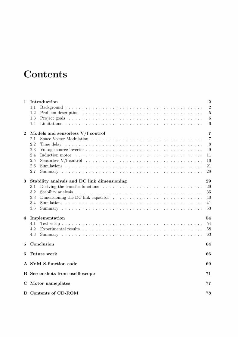
Fig. 2.1 shows the normalized reference voltages together with the triangular carrier wave. Thetriangular carrier wave having values between 1 and -1, it can be seen that the distances from thetop reference voltage to 1 is not the same as the distance from the bottom reference voltage to-1, this describes the case where the reference voltages are not centralized. Now the waveforms aremoved, using (2.2), so they become centralized within the triangular carrier wave as fig. 2.2 depicts.
7
2.2. TIME DELAY
7.55 7.6 7.65 7.7 7.75 7.8 7.85 7.9 7.95 8
x 10−4
−1
−0.8
−0.6
−0.4
−0.2
0
0.2
0.4
0.6
0.8
1
Time [s]7.55 7.6 7.65 7.7 7.75 7.8 7.85 7.9 7.95 8
x 10−4
−1
−0.8
−0.6
−0.4
−0.2
0
0.2
0.4
0.6
0.8
1
Time [s]
Figure 2.1: Uncentralized reference voltages. Figure 2.2: Centralized reference voltages.
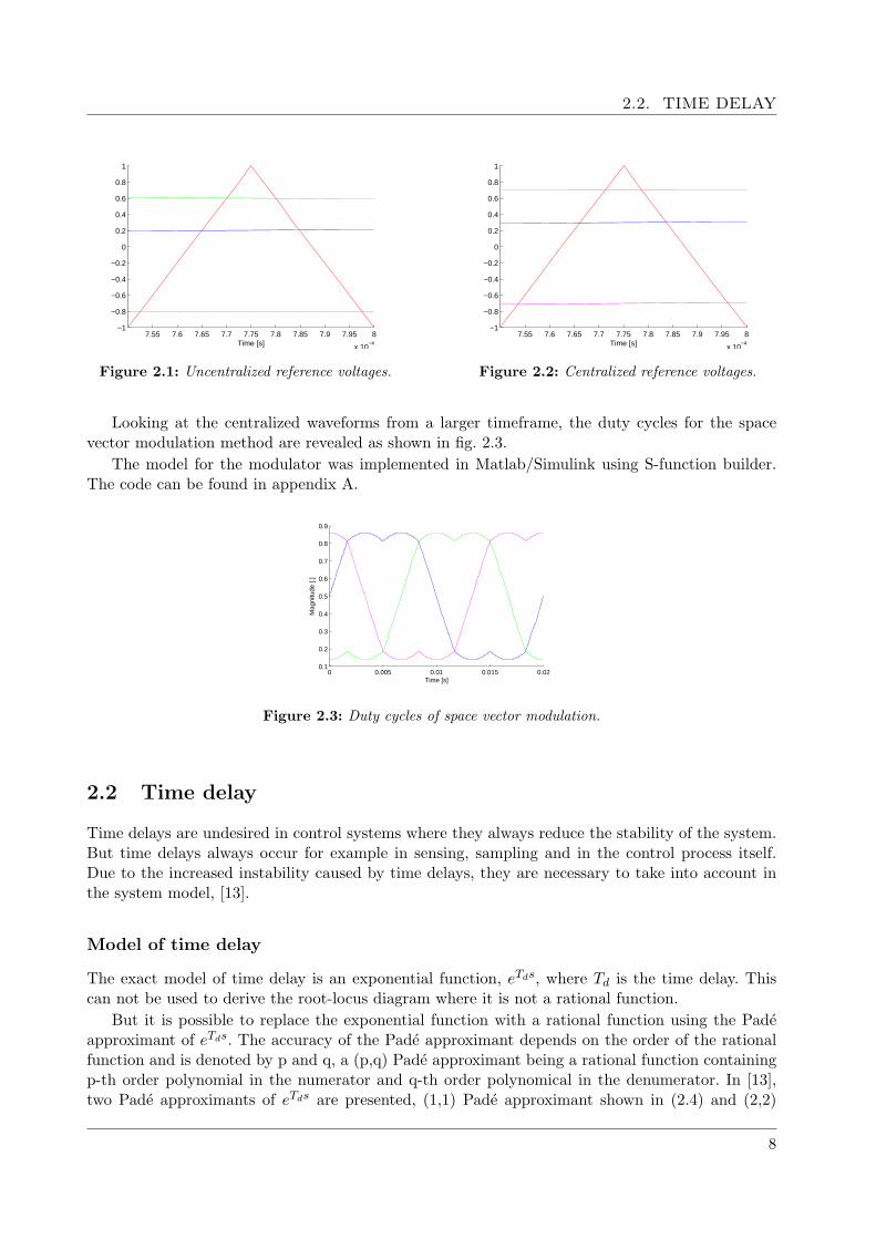
Looking at the centralized waveforms from a larger timeframe, the duty cycles for the spacevector modulation method are revealed as shown in fig. 2.3.
The model for the modulator was implemented in Matlab/Simulink using S-function builder.The code can be found in appendix A.
0 0.005 0.01 0.015 0.020.1
0.2
0.3
0.4
0.5
0.6
0.7
0.8
0.9
Time [s]
Mag
nitu
de [.
]
Figure 2.3: Duty cycles of space vector modulation.
2.2 Time delay
Time delays are undesired in control systems where they always reduce the stability of the system.But time delays always occur for example in sensing, sampling and in the control process itself.Due to the increased instability caused by time delays, they are necessary to take into account inthe system model, [13].
Model of time delay
The exact model of time delay is an exponential function, eTds, where Td is the time delay. Thiscan not be used to derive the root-locus diagram where it is not a rational function.
But it is possible to replace the exponential function with a rational function using the Padeapproximant of eTds. The accuracy of the Pade approximant depends on the order of the rationalfunction and is denoted by p and q, a (p,q) Pade approximant being a rational function containingp-th order polynomial in the numerator and q-th order polynomical in the denumerator. In [13],two Pade approximants of eTds are presented, (1,1) Pade approximant shown in (2.4) and (2,2)
8
CHAPTER 2. MODELS AND SENSORLESS V/F CONTROL
Pade approximant shown in (2.5).
eTds ∼=1− (Tds/2)1 + (Tds/2)
(2.4)
eTds ∼=1− (Tds/2) + (Tds)2/121 + (Tds/2) + (Tds)2/12
(2.5)
The Pade approximant corresponding to (2.5) is chosen for modeling the time delay where it ismore accurate with little increased complexity.
Block diagram of the model is shown in fig. 2.4.
( ) ( )( ) ( ) 221
2212
2
sTsTsTsT
dd
dd
+++−x x*
Figure 2.4: Block diagram of sample delay.
According to the project description there is a 2 samples delay within the system for a samplingfrequency of fs = 4 kHz. The sampling delay is therefore:
Td = 5 · 10−4 sec. (2.6)
2.3 Voltage source inverter
A model of the voltage source inverter (VSI) is necessary to transform the DC link voltage to thephase voltages applied to the load for given duty cycles.
Average model
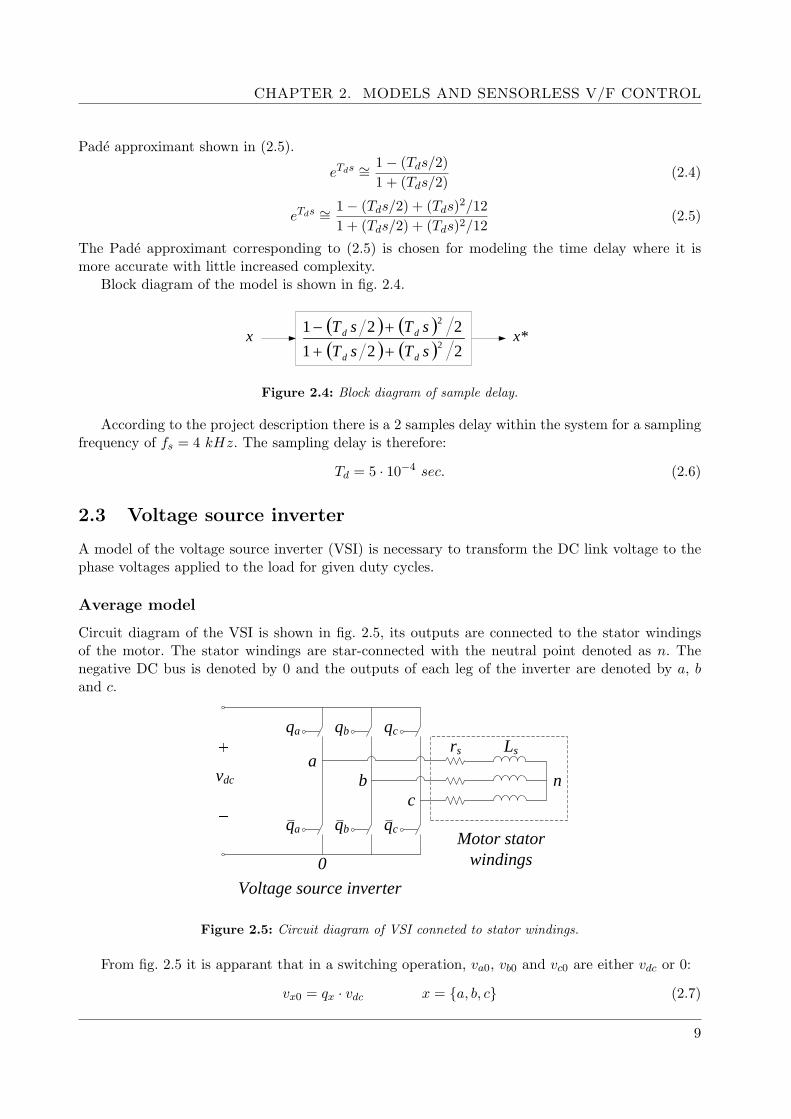
Circuit diagram of the VSI is shown in fig. 2.5, its outputs are connected to the stator windingsof the motor. The stator windings are star-connected with the neutral point denoted as n. Thenegative DC bus is denoted by 0 and the outputs of each leg of the inverter are denoted by a, band c.
vdc
rs
b
Ls
n
0
a
c
Motor stator windings
Voltage source inverter
qa
qa
qb
qb
qc
qc
Figure 2.5: Circuit diagram of VSI conneted to stator windings.
From fig. 2.5 it is apparant that in a switching operation, va0, vb0 and vc0 are either vdc or 0:
vx0 = qx · vdc x = a, b, c (2.7)
9

2.3. VOLTAGE SOURCE INVERTER
where qx is the switching state of the leg, qx = 1 meaning that the upper switch is conductiongwhile the lower is blocking and qx = 0 meaning the opposite.
For an average model the switching states are replaced with the duty cycles dx of each leg:
vx0 = dx · vdc x = a, b, c (2.8)
Then each phase voltage can be described by:
vxn = vx0 − vn0 x = a, b, c (2.9)
where vn0 is [1]:
vn0 =va0 + vb0 + vc0
3(2.10)
Putting (2.8) and (2.10) in (2.9) gives the average model of the VSI:
van = (2da − db − dc)vdc3
vbn = (2db − da − dc)vdc3
(2.11)
vcn = (2dc − db − da)vdc3
The DC link current can be derived using Kirchoffs current law. The DC link current is thetotal current from all branches:
idc = daia + dbib + dcic (2.12)
To fit with the motor model the phase voltages have to be transformed to the stationary referenceframe using (2.13).
vα =23
(van −
12vbn −
12vcn
)vβ =
23
√3
2(vbn − vcn) (2.13)
Block diagram of the VSI model is shown in fig. 2.6.
10

CHAPTER 2. MODELS AND SENSORLESS V/F CONTROL
x+
−−
32
31
31
x+
−−
32
31
31
x+
−−
32
31
31
da
db
dc
db
da
dc
dc
da
db
vdc
van
vbn
vcn
vαn
vβn
Figure 2.6: Block diagram of VSI.
2.4 Induction motor
A model of the squirrel cage induction motor (SCIM) is necessary to see the influence of differentinverter output voltages on the motor for different load torques. The selected model of the IM isthe Γ model where it is well suited for analysis of drives using the V/f control strategy [14].
IM equations in dq0 reference frame
Equations that describe the dynamic behavior of the IM are shown in (2.14) and (2.15), [15].
~vabcs = rs~iabcs + Lsp~iabcs + γL′mp(~i′abcre
jθr
γ) (2.14)
γ~v′abcr = γ2r′r~i′abcrγ
+ γ2L′rp~i′abcrγ
+ γL′mp(~iabcse−jθr) (2.15)
where Ls = Lls + L′m and L′r = L′lr + L′m. Lls and L′lr being the leakage inductances of the statorand rotor, respectively, and L′m the mutual inductance between stator and rotor windings.
The parameter γ is the turns-ratio between the stator and rotor. It arises from the transformeraction of the IM and can be chosen completely arbitarily for a squirrel cage IM, [15]. But it willremain undefined for now. (2.14) and (2.15) can be simplified by using the notation:
~vabcr = γ~v′abcr (2.16)
~iabcr =~i′abcrγ
(2.17)
Lm = γL′m (2.18)Lr = γ2L′r (2.19)rr = γ2r′r (2.20)
11
2.4. INDUCTION MOTOR
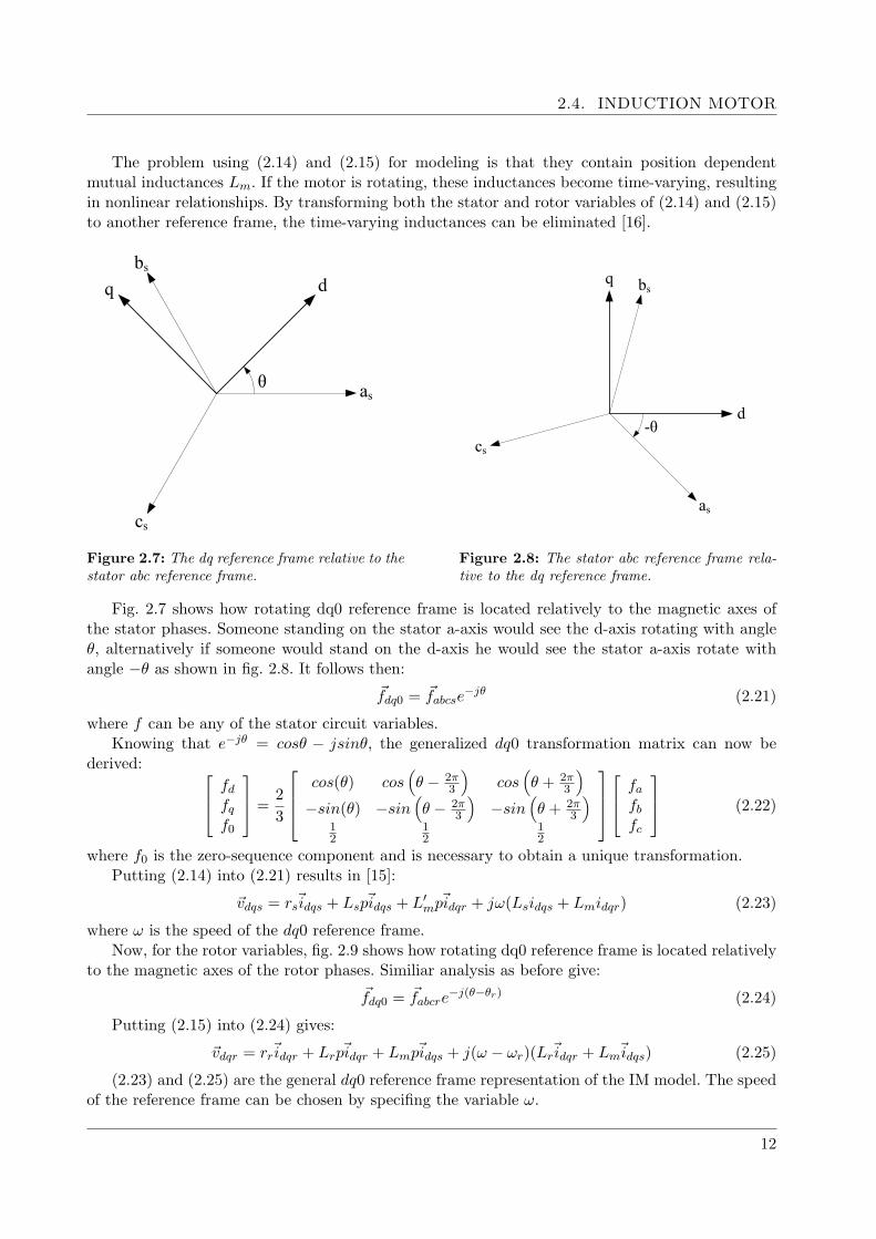
The problem using (2.14) and (2.15) for modeling is that they contain position dependentmutual inductances Lm. If the motor is rotating, these inductances become time-varying, resultingin nonlinear relationships. By transforming both the stator and rotor variables of (2.14) and (2.15)to another reference frame, the time-varying inductances can be eliminated [16].
as
bs
cs
dq
θ
as
bs
cs
d
q
-θ
Figure 2.7: The dq reference frame relative to thestator abc reference frame.
Figure 2.8: The stator abc reference frame rela-tive to the dq reference frame.
Fig. 2.7 shows how rotating dq0 reference frame is located relatively to the magnetic axes ofthe stator phases. Someone standing on the stator a-axis would see the d-axis rotating with angleθ, alternatively if someone would stand on the d-axis he would see the stator a-axis rotate withangle −θ as shown in fig. 2.8. It follows then:
~fdq0 = ~fabcse−jθ (2.21)
where f can be any of the stator circuit variables.Knowing that e−jθ = cosθ − jsinθ, the generalized dq0 transformation matrix can now be
derived: fdfqf0
=23
cos(θ) cos
(θ − 2π
3
)cos
(θ + 2π
3
)−sin(θ) −sin
(θ − 2π
3
)−sin
(θ + 2π
3
)12
12
12
fafbfc
(2.22)
where f0 is the zero-sequence component and is necessary to obtain a unique transformation.Putting (2.14) into (2.21) results in [15]:
~vdqs = rs~idqs + Lsp~idqs + L′mp~idqr + jω(Lsidqs + Lmidqr) (2.23)
where ω is the speed of the dq0 reference frame.Now, for the rotor variables, fig. 2.9 shows how rotating dq0 reference frame is located relatively
to the magnetic axes of the rotor phases. Similiar analysis as before give:~fdq0 = ~fabcre
−j(θ−θr) (2.24)
Putting (2.15) into (2.24) gives:
~vdqr = rr~idqr + Lrp~idqr + Lmp~idqs + j(ω − ωr)(Lr~idqr + Lm~idqs) (2.25)
(2.23) and (2.25) are the general dq0 reference frame representation of the IM model. The speedof the reference frame can be chosen by specifing the variable ω.
12

CHAPTER 2. MODELS AND SENSORLESS V/F CONTROL
dq
θ
ar
as
br
cr
θr
θ θr
Figure 2.9: The dq reference frame relative to the rotor abc reference frame.
Γ model
In (2.14) and (2.15) the turns-ratio parameter γ was left undefined. The most common definitionof γ is the real turns-ratio:
γ =Ns
Nr(2.26)
where Ns is the number of windings on the stator and Nr is the number of windings on the rotor.This results in real leakage inductance model based on the datasheet from the designer, [15].
The equivalent circuit representation for this arrangement can be seen in fig. 2.10.
vdqs
rs Lsl
Lm
Lrl rr
jωr(Lmidqs+Lridqr)idqridqs
Figure 2.10: T-model of equivalent circuit.
But defining γ as:
γ =LsL′m
(2.27)
puts all the leakage inductance on the rotor and is convenient for drives using the V/f control, [14].It is therefore used for the IM model.
The new parameters of the motor can be calculated using (2.20) and (2.27).
Lm = Ls (2.28)Lr = γ2L′lr + γLls + Ls (2.29)rr = γ2r′r (2.30)
The IM model then looks like:
~vdqs = rs~idqs + Lsp~idqs + Lsp~idqr + jωLs(~idqs +~idqr) (2.31)
13

2.4. INDUCTION MOTOR
~vdqr = rr~idqr + Lrp~idqr + Lsp~idqs + j(ω − ωr)(Lr~idqr + Ls~idqs) (2.32)
This changes the equivalent circuits representation as seen in fig. 2.11. To fit with the equations,another inductance, LL = γ2L′lr + γLls, is defined as the rotor inductance.
vdqs
rs
Ls
LL rr
jωr(Lsidqs+Lridqr)idqridqs
Figure 2.11: Γ-model of equivalent circuit.
Constructing the model
To build the model in Matlab/Simulink (2.31) and (2.32) have to be split to their d and q compo-nents and put in the s-domain.
vds = rsids + Lssids + Lssidr − ωLs(iqs + iqr) (2.33)vqs = rsiqs + Lssiqs + Lssiqr + ωLs(ids + idr) (2.34)vdr = rridr + Lrsidr + Lssids − (ω − ωr)(Lriqr + Lsiqs) (2.35)vqr = rriqr + Lrsiqr + Lssiqs + (ω − ωr)(Lridr + Lsids) (2.36)
The model is build using the stationary reference frame, therefore ω = 0. The stator currentsare derived by isolating ids in (2.33) and iqs in (2.34):
ids =1
sLs + rs(vds − sLsidr) (2.37)
iqs =1
sLs + rs(vqs − sLsiqr) (2.38)
Block diagram of the model for obtaining stator currents is show in fig. 2.12.The rotor currents can be derived from (2.35) and (2.36) by isolating idr and iqr and knowing
that vdr = vqr = 0 for SCIM:
idr =1
sLr + rr(−ωr (Lsiqs + Lriqr)− sLsids) (2.39)
iqr =1
sLr + rr(ωr (Lsids + Lridr)− sLsiqs) (2.40)
(2.37)-(2.40) define the IM electrical system model. The block diagram for the rotor currentmodel is shown in fig. 2.13.
For the mechanical system the electromechanical power Pem produced by the IM is defined as,[15]:
Pem =32PωmL
′m (iqsidr − idsiqr) =
32PωmLs (iqsidr − idsiqr) (2.41)
14

CHAPTER 2. MODELS AND SENSORLESS V/F CONTROL
ss rsL +1
ss
s
rsLsL+
dsi
dsv
dri
ss rsL +1
ss
s
rsLsL+
qsv
qri
qsi+−
+−
Figure 2.12: Electrical system - Stator currents.
sLqsi
rL −−
ss rsL +1
++
×+−
ss
s
rsLsL+
qri
dsi
rωdri
sL
rLss rsL +
1
×+−
ss
s
rsLsL+
rω
dsi
dri
qsi
qri
Figure 2.13: Electrical system - Rotor currents.
15

2.5. SENSORLESS V/F CONTROL
where P is the number of pole-pairs of the IM, L′m = Ls because of the previously defined γ andωm is the mechanical speed of the rotor which is related to the electrical speed by:
ωr = P · ωm (2.42)
The produced electromechanical torque Tem is then:
Tem =Pemωm
=32PLs (iqsidr − idsiqr) (2.43)
To describe the electromechanical behaviour of the IM the simplest form is used [15]:
Tem = Jdωmdt
+ TL (2.44)
where J is the inertia of the shaft and TL is the applied load torque.Rearranging (2.44) and transforming to s-domain gives the rotor speed in mechanical degrees:
ωm =1Js
(Tem − TL) (2.45)
Block diagram of the mechanical system is shown in fig. 2.14.
qsi +−
qridsi
×
×
−+
dri
sPL23 emT
LT Js1
mω
s1
mθ
Figure 2.14: Mechanical system of IM model.
2.5 Sensorless V/f control
To be consistent with project purpose of a low-cost design, a sensorless speed controller has to beimplemented. Because of its simplicity, V/f control is widely used despite its inferior performancecompared to the vector control methods. To increase accuracy, the open loop V/f control requirescompensation for stator resistance voltage drop and slip frequency. Stator resistance voltage dropcan be easily compensated by the knowledge of stator resistance but slip compensation requiresknowledge of the rotor speed which can be available through an encoder or speed tachometer. Butthe slip frequency can also be obtained without the sensor using stator voltages and currents. Thispreserves the mechanical robustness of the SCIM and decreases the cost of the drive, [17].
The method used is explained in [18] and estimates the slip speed by estimating the electro-magnetic torque and the flux component of the stator current in the rotor flux oriented referenceframe. The stator voltage drop is partially estimated using the torque component of the statorcurrent in the rotor flux oriented reference frame. This is announced to be more efficient than fullcompensation in keeping the flux from saturating.
16

CHAPTER 2. MODELS AND SENSORLESS V/F CONTROL
Open loop V/f control
To explain the theory behind the open loop V/f control the dynamic model of the SCIM in syn-chronous reference frame has to be observed, [17]:
sλesd = vesd − rsiesd + ωeλesq (2.46)
sλesq = vesq − rsiesq + ωeλesd (2.47)
where the superscript e denotes a variable in the synchronous reference frame.In the synchronous reference frame all stator variables become constant during steady state.
Also, if the flux vector is assigned to the d-axis the flux component on the q-axis is zero. (2.46) and(2.47) then reduce to:
vesd = rsiesd (2.48)
vesq = rsiesq + ωeλs (2.49)
If the stator resistance is neglected the stator voltage vector becomes:
|~vs| ≈ ωeλs (2.50)
(2.50) shows that constant flux can be obtained by keeping the ratio between frequency andstator voltage constant. It is desired to hold the flux at its rated value, thus for a given referencefrequency fref the peak value of the stator voltage should be:
|Vs| =Vnfnfref (2.51)
where Vn and fn are the nominal voltage and frequency of the motor, respectively.
Rotor flux observer
The dynamic model of the SCIM can be described by the following equations in the αβ referenceframe using the Γ-model:
vsα = rsisα + sλsα (2.52)vsβ = rsisβ + sλsβ (2.53)
0 = rrirα + sλrα + ωrλrβ (2.54)0 = rrirβ + sλrβ − ωrλrα (2.55)
Where the flux linkages are expressed as:
λsα = Ls (isα + irα) (2.56)λsβ = Ls (isβ + irβ) (2.57)λrα = Lsisα + Lrirα (2.58)λrβ = Lsisβ + Lrirβ (2.59)
The stator flux can be estimated by isolating the stator flux component in (2.52) and (2.53):
17

2.5. SENSORLESS V/F CONTROL
λsα =∫
(vsα − rsisα) dt (2.60)
λsβ =∫
(vsβ − rsisβ) dt (2.61)
To prevent the DC drift and initial value problem of the pure integrator it is replaced by amodified integrator explained in [19]. Block diagram of the modified integrator is shown in fig. 2.15,where L is the nominal stator flux.
sss riu αα −+
c
c
s ωω+
cs ω+1
Polarto
Cartesian
+
c
c
s ωω+
cs ω+1
Cartesianto
Polar
sss riu ββ −
λ
eθ
L
αλs
βλs
Figure 2.15: Modified integrator.
From (2.56) and (2.57) the rotor currents can be expressed as:
irα =λsαLs− isα (2.62)
irβ =λsβLs− isβ (2.63)
Inserting into (2.58) and (2.59) gives the rotor flux:
λrα =LrLsλsα − (Lr − Ls) isα (2.64)
λrβ =LrLsλsβ − (Lr − Ls) isβ (2.65)
The rotor position can now be obtained as the angle between the rotor flux components, λrαand λrβ :
θr = arctan(λrβλrα
)(2.66)
Thus all variables can be transformed to the rotor flux oriented reference frame. The imple-mentation of the rs and slip compensator requires the stator currents in the rotor flux orientedreference frame:
irsd = isα cos θr + isβ sin θr (2.67)irsq = −isα sin θr + isβ cos θr (2.68)
where the superscript r denotes variables represented in the rotor flux oriented reference frame.
18

CHAPTER 2. MODELS AND SENSORLESS V/F CONTROL
Stator resistance compensation
The stator resistance voltage drop can be fully compensated using the triangular relationship [20]:
Vs = Isrs cosφ+√E2s − (Isrs sinφ)2 (2.69)
But this method tends to overcompensate the voltage resulting in saturation of the stator fluxespecially when the load torque decreases, [18]. This method is especially useful in low frequencysituations like starting the SCIM with large load. For low stator frequency the rotor leakage issmall enough to be omitted. The T-model equivalent circuit of the induction motor then becomesas shown in fig. 2.16. Drawing the vector diagram of this circuit, fig. 2.17, shows that the isq currentis now directly proportional to the airgap emf vector Em. Therefore, to maintain constant airgapflux, only the stator resistance voltage drop related to the isq component needs to be compensated.
rs
Lls
Lm rr/S
isdisq
sir
svr
EmEs Els
isd
isq
sir
svr
EmEs
Els
q
d
ss rir
Figure 2.16: Simplified T-model of SCIM at lowfrequency.
Figure 2.17: Vector diagram of SCIM at low fre-quency.
The stator voltage with added compensation then becomes:
V ∗s = Vs + Emirsq (2.70)
While this approximation is only valid at a low stator frequency it is applicable where projectis limited to low speed performance.
Slip compensation
In the rotor flux oriented reference frame the slip speed ωsl can be denoted as, [18]:
ωsl =Temr
′r
P (L′m)2 i2sd(2.71)
19

2.5. SENSORLESS V/F CONTROL
In the Γ-model, (2.71) becomes:
ωsl =Temr
′r
PL2si
2sd
(2.72)
Knowing that the electromagnetic torqe can be described by:
Tem =32P (λsαisβ − λsβisα) (2.73)
and the d-component of the stator current can be obtained from (2.67), the slip speed can easily becalculated and added to the reference speed. Block diagram of the whole sensorless control schemeis shown in fig. 2.18 and block diagram of the open loop V/f control is shown in fig. 2.19. Lowpassfilters are necessary to minimize ripple in frequency reference due to ripple in feedback signals, vsα,vsβ, isα and isβ.
++
s1
r*
Rotorflux
observer
++
Open loopV/f control
Slipcompensator
rscompensator
isdTem isq
e
sl
Vs
e
vsα vsβ isα isβ
LowpassFilter
LowpassFilter
LowpassFilter
Figure 2.18: Block diagram of sensorless V/f control.
20
CHAPTER 2. MODELS AND SENSORLESS V/F CONTROL
s1
2
2≤
P/60
Vn/fn
nreffref
Vref
ref ref
Transform to
three phase
voltages
vabc-ref
Externalreset
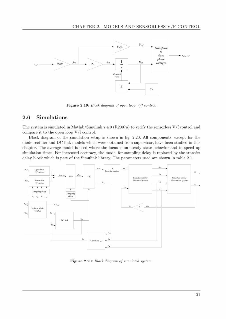
Figure 2.19: Block diagram of open loop V/f control.
2.6 Simulations
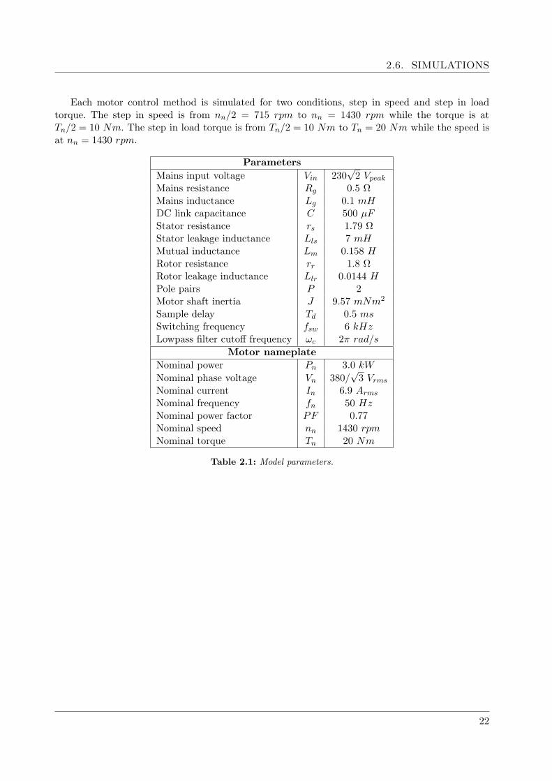
The system is simulated in Matlab/Simulink 7.4.0 (R2007a) to verify the sensorless V/f control andcompare it to the open loop V/f control.
Block diagram of the simulation setup is shown in fig. 2.20. All components, except for thediode rectifier and DC link models which were obtained from supervisor, have been studied in thischapter. The average model is used where the focus is on steady state behavior and to speed upsimulation times. For increased accuracy, the model for sampling delay is replaced by the transferdelay block which is part of the Simulink library. The parameters used are shown in table 2.1.
Open loopV/f control
SVM
nref
vabc-ref
Transformationvabc v
Induction motorElectrical system
Induction motorMechanical system
ir
ir
is
is
Te
ωm
ωr
3-phase diode rectifier
vgrid
DC link
igrid
Calculate idc
dabc
is
is
vdc
idc
idc
vdc idi
dabc
vs vs is is
VSI
Samplingdelay
SensorlessV/f control
Sampling delay
dabc
P ωmωr
nref
Figure 2.20: Block diagram of simulated system.
21
2.6. SIMULATIONS
Each motor control method is simulated for two conditions, step in speed and step in loadtorque. The step in speed is from nn/2 = 715 rpm to nn = 1430 rpm while the torque is atTn/2 = 10 Nm. The step in load torque is from Tn/2 = 10 Nm to Tn = 20 Nm while the speed isat nn = 1430 rpm.
ParametersMains input voltage Vin 230
√2 Vpeak
Mains resistance Rg 0.5 ΩMains inductance Lg 0.1 mHDC link capacitance C 500 µFStator resistance rs 1.79 ΩStator leakage inductance Lls 7 mHMutual inductance Lm 0.158 HRotor resistance rr 1.8 ΩRotor leakage inductance Llr 0.0144 HPole pairs P 2Motor shaft inertia J 9.57 mNm2
Sample delay Td 0.5 msSwitching frequency fsw 6 kHzLowpass filter cutoff frequency ωc 2π rad/s
Motor nameplateNominal power Pn 3.0 kWNominal phase voltage Vn 380/
√3 Vrms
Nominal current In 6.9 ArmsNominal frequency fn 50 HzNominal power factor PF 0.77Nominal speed nn 1430 rpmNominal torque Tn 20 Nm
Table 2.1: Model parameters.
22

CHAPTER 2. MODELS AND SENSORLESS V/F CONTROL
Case 1a: Open loop V/f control - Speed step
Fig.s 2.21 and 2.23 show the DC link voltage and the DC link current, that is the current goinginto the inverter. Due to the speed step, the DC link current increases as the stator voltage hasbeen increased over the stator resistance. It can be observed that the average value of the DClink voltage decreases which should not occur if compared to simulations using PLECS in section3.4. It is also observed that the ripples are increased in the DC link voltage which is also unusualwhere the diode rectifier always soft-switches. Looking closer at the DC link voltage shows that itonly contains harmonics of 300 Hz from the diode rectifier and no switching harmonics. This wasexpected as the average model was being used. The ripple in the DC link voltage should thereforenot increase. This could be caused by poor accuracy of the model that was used in the simulationbut this is not of so much concern in this section where the focus is on comparing the open loopV/f control to the sensorless V/f control.
Figure 2.21: V/f control. DC link voltage at speedstep.
Figure 2.22: V/f control. Zoom on DC link volt-age.
Due to doubling in speed reference, the V/f control doubles the voltage which is in correspon-dance with the V/f control, fig. 2.24.
Figure 2.23: V/f control. DC link current atspeed step.
Figure 2.24: V/f control. Peak value of referencevoltage.
The rotor speed and electromagnetic torque are affected by the fluctuations in the DC linkvoltage and contain rippled content. The torque is then the same before and after the speed stepwhere no change in load occured. The rotor speed is changed but is lower than the reference due tostator resistance and slip, where applied load is Tn/2 = 10 Nm. These factors are not taken intoaccount in the open loop V/f control and therefore a large error in rotor speed is encountered.
23

2.6. SIMULATIONS
Figure 2.25: V/f control. Rotor speed at speedstep.
Figure 2.26: V/f control. Electromagnetic torqueat speed step.
Case 1b: Open loop V/f control - Torque step
At the time of torque step, the DC link current is increased as the torque is only proportional tothe current when the flux is held constant, fig. 2.28. The DC link voltage should not be affectedbut actually get affected due to inaccurate modeling, 2.27.
Figure 2.27: V/f control. DC link voltage attorque step.
Figure 2.28: V/f control. DC link current attorque step.
As seen from fig. 2.29, the rotor speed is even further from the reference both due to the increasein slip and increase in stator current. It can be observed in fig. 2.24 that no change occurs in thereference stator voltage at the instance of torque step, at time t = 1 sec.
The torque step increases the electromagnetic torque of the motor which needs to match theload torque to maintain speed, fig. 2.30.
24

CHAPTER 2. MODELS AND SENSORLESS V/F CONTROL
Figure 2.29: V/f control. Rotor speed at torquestep.
Figure 2.30: V/f control. Electromagnetic torqueat torque step.
Case 2a: Sensorless V/f control - Speed step
Now, the stator voltages and currents are fed back to the V/f controller to allow compensation forstator resistance and slip. But due to ripples in current and voltage and sample delays, the sensedsignals also contain ripples which induces more ripples. This is seen from the DC link current andvoltage which fluctuate more erratically than before, fig.s 2.31 and 2.32.
Figure 2.31: Sensorless V/f control. DC linkvoltage at speed step.
Figure 2.32: Sensorless V/f control. DC link cur-rent at speed step.
It can be seen from fig. 2.33 that the reference voltage saturates at the instance of the speed step.This is because the current is limited in the sensorless V/f controller. But the reference voltage isnow higher than in Case 1a because the voltage drop over the stator resistance is taken into account.The slip speed is seen in fig. 2.34 and its response is bounded by the lowpass filters in the controller.The lowpass filters are 1st order and are all put to rather low cutoff frequency (ωc = 2π) whichintroduces slow response with low harmonic content. If examined closely, it can be seen that thesensed slip speed reaches steady state little before t = 2 sec in fig. 2.34, the load step discussed innext subsection is applied at time t = 1 sec.
Because of the sensorless control the rotor speed is now closer to the reference than in Case 1abut the speed is a little bit over estimated. The torque is similiar as in Case 1a but it is seen thatthe ripples in the reference voltage propagate to the torque, fig. 2.36.
25

2.6. SIMULATIONS
Figure 2.33: Sensorless V/f control. Peak valueof reference voltage.
Figure 2.34: Sensorless V/f control. Sensed slipspeed.
Figure 2.35: Sensorless V/f control. Rotor speedat speed step.
Figure 2.36: Sensorless V/f control. Electromag-netic torque at speed step.
26

CHAPTER 2. MODELS AND SENSORLESS V/F CONTROL
Case 2b: Sensorless V/f control - Torque step
As in case 1b the torque step increases the DC link current resulting in lower DC link voltage.The DC link voltage and current fluctuate more erratically because of the ripples in the referencevoltage.
Figure 2.37: Sensorless V/f control. DC linkvoltage at torque step.
Figure 2.38: Sensorless V/f control. DC link cur-rent at torque step.
The rotor speed decreases due to the load step but the speed controller increases the speed toalmost the same value as before the load step. The electromagnetic torque follows the load torqueand fluctuates due to the DC link current and reference voltage ripples.
Figure 2.39: Sensorless V/f control. Rotor speedat torque step.
Figure 2.40: Sensorless V/f control. Electromag-netic torque at torque step.
27

2.7. SUMMARY
2.7 Summary
Components of the system, delay, modulation and a control strategy have all been modeled andstudied in this chapter except for the diode rectifier and DC link models which were obtained fromsupervisor. Although the model for time delay was not used in simulations it was necessary toderive where it will be used in next chapter.
Simulations showed that better speed accuracy is acquired with the sensorless V/f control butmore ripples are introduced in rotor speed and electromagnetic torque. These ripples are caused byripples in stator currents and voltages which causes ripples in the calculated slip speed and voltagereferences. Due to this, the ripples basically propagate through the system and become more severebecause of sampling delay. As fast dynamics are not of concern in the system, a solution could be toput a filter on all feedback signals. This would give slower response but ripples would be reduced.In practice, the stator voltages would at least have to be filtered because of the PWM controlledinverter. But because an average model was used in the simulation, filtering of stator voltages wasnot necessary.
28
CHAPTER 3. STABILITY ANALYSIS AND DC LINK DIMENSIONING
Chapter 3
Stability analysis and DC linkdimensioning
In this chapter a small signal model of the system is obtained and the corresponding transfer func-tions are used for stability analysis and to evaluate the effect of different parameters on stability.Then the converter considered in the project and the converter used in implementation from Dan-foss are compared with simulations. Finally, the stability analysis is evaluated by attempts to createan unstable condition with simulations based on the stability analysis.
3.1 Deriving the transfer functions
With a small DC link capacitor the DC link voltage fluctuates heavily. To examine if this cancause the system to become unstable the frequency converter has to be linearized in order to find atransfer function describing the system. The system has two inputs, grid side voltage and frequencyreference for the SCIM. To investigate the stability behavior on the DC link voltage caused by theseinputs, a linear relationship between these terms is needed. In this section these relationships arederived.
Simplified model of frequency converter
Circuit diagram of the frequency converter without the inverter is shown in fig. 3.1. To obtain thelinearized model of the frequency converter, a simplified model will be used, shown in fig. 3.2, [5].The simplified model assumes that the diode rectifier is always working in discontinuous conductionmode. Therefore only two diodes conduct at once, [1]. This assumption can be made where the onlyinductance involved is the mains inductance which is low in practice and causes a discontinuousgrid side current, [2]. In the simplified model the mains impedances have been moved to the DClink and the diode rectifier has been replaced with a voltage source which has the output of anideal diode rectifier.
From the simplified circuit the following system model can be derived:
vdc =1
s2CL′g + sCR′g + 1vg +
sL′g +R′gs2CL′g + sCR′g + 1
idc (3.1)
where L′g and R′g are defined as:
L′g = 2Lg R′g = 2Rg + 3ωgLg/π (3.2)
29

3.1. DERIVING THE TRANSFER FUNCTIONS
vdc
Rg Lgvga
idcidi
iga
C vdc
R′g L′g idcidi
Cvg
Figure 3.1: Circuit diagram of frequency con-verter.
Figure 3.2: Simplified circuit diagram of fre-quency converter.
where ωg is the angular frequency of the grid side voltage and the term 3ωgLg/π denotes thenonohmic losses due to noninstantaneous commutation of diodes, [1] [5].
Where (3.1) is linear, the small signal model can easily be obtained:
vdc =1
s2CL′g + sCR′g + 1vg +
sL′g +R′gs2CL′g + sCR′g + 1
idc (3.3)
where the transfer functions that describe the system are:
Gvg(s) =
(vdcvg
)idc=0
=1
s2CL′g + sCR′g + 1(3.4)
Gvi(s) =(vdc
idc
)vg=0
=sL′g +R′g
s2CL′g + sCR′g + 1(3.5)
But where idc is not a control variable, Gvi is not useful in its present form. idc has to be replacedby a control variable, which in this case is ωe.
Relationship between idc and ωe
As mentioned before the transfer functions have to give a linear relationship between vdc and thetwo control inputs of the system, vg and ωe. Before being able to derive these transfer functions alinear relationship has to be found between idc and ωe resulting in the correpsonding small signalmodel between these variables.
The sum of all losses in the inverter and motor should equal the DC link power:
vdcidc = Pinv + PCu + Pf + Pem (3.6)
where Pinv denotes the losses in the inverter, PCu the resistive losses in the SCIM, Pf the corelosses and Pem the power converted to electromagnetic power. Assuming that the losses are smallcompared to the produced electrommagnetic power and that the system is operating in steadystate, (3.6) can be simplified to:
vdcidc = Pem (3.7)
The electromagnetic power can be expressed as a function of the electromagnetic torque Temand electrical speed ωe.
Pem = TemωeP
(3.8)
P being the number of pole-pairs.
30

CHAPTER 3. STABILITY ANALYSIS AND DC LINK DIMENSIONING
Then idc can be expressed as:
idc =Temvdc
ωeP
(3.9)
The modulation coefficient is defined as, [21]:
ma =π
2vsvdc
(3.10)
Isolating vdc and inserting into (3.9) gives:
idc =2π
Temvs
ma
Pωe (3.11)
Now, (3.11) is nonlinear because it contains products of time-varying variables. (3.11) can belinearized by denoting each variable by its quiscent value and small AC variation at a certainoperating point, [2]. Quiscent values are denoted by a captial letter or are followed by q notation.Small AC varying variables are denoted with a . Linearizing (3.11) gives:
Idc + idc =2π
1P
T qem + TemVs + vs
(Ωe + ωe) (Ma + ma) (3.12)
After few steps (3.12) becomes:
Idc + Vsidcvs
=2π
1P
(T qem
ωevs
+ ΩeTemvs
)(Ma + ma) (3.13)
Now, vs can be replaced using the V/f ratio from (2.51). This ratio is linear and the small signalmodel is therefore easily obtained:
vs =Vnωnωe (3.14)
Putting (3.14) into (3.13) and isolating idc then gives:
idc =2π
1P
(ΩeVnωnVs
Temvs
+T qemVs
)(Ma + ma) ωe −
IdcVnωnVs
ωe (3.15)
Calculating terms:
idc =2π
1P
MaΩeVnωnVs
Temvs
ωe︸ ︷︷ ︸1st order
+ΩeVnωnVs
Temvs
maωe︸ ︷︷ ︸2nd order
+MaT qemVs
ωe︸ ︷︷ ︸1st order
+T qemVs
maωe︸ ︷︷ ︸2nd order
− IdcVnωnVs
ωe︸ ︷︷ ︸1st order
(3.16)
Now, (3.16) has been split up into 1st order and 2nd order AC terms. The 1st order AC termsare linear but the 2nd order AC terms contain products of time-varying AC quantities and arethereby nonlinear. Provided that the AC varying quantities are small, the 2nd order AC terms canbe neglected, [2]. Then, (3.16) reduces to the desired relationship between idc and ωe::
idc =
2π
Ma
P
ΩeVnωnVs︸ ︷︷ ︸
Constant
Temvs︸ ︷︷ ︸
SCIM
+2π
Ma
P
T qemVs− IdcVnωnVs︸ ︷︷ ︸
Constant
ωe (3.17)
31

3.1. DERIVING THE TRANSFER FUNCTIONS
But the term Tem/vs involves the SCIM, which has yet to be evaluated. Inserting (3.17) into(3.3) would give a product of two transfer functions, Gvi and Tem/vs. So two systems are involved,the converter and the SCIM. This can be simplified considerably by comparing the poles of thetwo systems. Knowing that if a system contains poles that are insignificant compared to the moredominant system, the dynamics of the system can be ignored. The insignificant system can conse-quently be replaced by a gain. A diagram showing position of dominant and insignificant poles inthe s-plane are shown in fig. 3.3. As a rule of thumb, in order to disregard the insignificant polesthe ratio b/a needs to be 5 or larger, [22].
Dominating poles
Insignificantpoles
-b -a
Unstableregion
Figure 3.3: Diagram showing locations of dominating and insignificant poles.
If the converter is dominant the dynamics of the SCIM can be ignored and Tem/vs can bereplaced by a constant T qem/Vs in (3.17). But if the SCIM is more dominant, the converter has littleeffect in this term. It can therefore be omitted where all instability behavior is determined by theSCIM which is beyond the scope of this project where the focus is on instability caused by theconverter.
But in order to check which system is more dominant the SCIM needs to be linearized to seethe pole locations.
Linearized model of SCIM
A linearized small signal model of the SCIM using the Γ-model in the dq0-synchronous referenceframe is shown in (3.18), [16].
vdsvqsvdrvqrTL
=
rs + sLs −ωeLs sLs −ωeLs 0ωeLs rs + sLs ωeLs sLs 0sLs −ωslLs rr + sLr −ωslLr LsIqs + LrIqrωslLs sLs ωslLr rr + sLr −LsIds − LrIdr−LsIqr LsIdr LsIqs −LsIds sJ
idsiqsidriqrωr
(3.18)
where ωsl = ωe − ωr is the slip speed and Ids, Iqs, Idr, Iqr are the desired operating point and arefound by simulation.
As described in [16], it is convenient to divide the derivative and non-derivative terms into twomatrices:
32

CHAPTER 3. STABILITY ANALYSIS AND DC LINK DIMENSIONING
E =
Ls 0 Ls 0 00 Ls 0 Ls 0Ls 0 Lr 0 00 Ls 0 Lr 00 0 0 0 −J
(3.19)
F = −
rs −ωeLs 0 −ωeLs 0ωeLs rs ωeLs 0 0
0 −ωslLs rr −ωslLr LsIqs + LrIqrωslLs 0 ωslLr rr −LsIds − LrIdr−LsIqr LsIdr LsIqs −LsIds 0
(3.20)
So the the matrix equation takes the form:
u = (sE− F) x (3.21)
whereu =
[vds vqs vdr vqr TL
]Tx =
[ids iqs idr iqr ωr
]T(3.22)
and a linear differential equation of the SCIM can be directly obtained from (3.21), [16]:
sx = E−1Fx + E−1u (3.23)
For the SCIM it is desired to obtaine a linear relationship between the peak value of the statorvoltage vs and the produced electromagnetic torque Tem. This gives the variation in Tem for adisturbance in vs.
In general control theory while examining one disturbance all other disturbances can be put tozero. Therefore all inputs except for vds and vqs are put to zero in the input vector u:
u = [vds vqs 0 0 0 0]T (3.24)
Now, the stator voltage in the synchronous dq-reference frame has to be transformed to thepeak value of the stator voltage in the abc-reference frame using (3.25) and (3.26), [16]:
vds = vs cos(θ − θe) (3.25)
vqs = −vs sin(θ − θe) (3.26)
where θ is the angle of the dq0-reference frame and θe is the angle of the input voltage.In the synchronous reference frame, θ is rotating at synchronous speed which is determined by
the input voltage with angle θe. θ and θe are therefore travelling at the same speed which makesthe difference between them a constant. This constant depends only on the initial position of thereference frame which can be chosen arbitarily. Here, the d-axis is chosen to be aligned with thea-axis, therefore θ − θe = 0:
vds = vs cos 0 (3.27)
vqs = −vs sin 0 (3.28)
Assuming that the voltage changes only in magnitude but not in phase, ensuring θe − θ =constant, (3.27) and (3.28) are linear and the small signal model can be obtained directly:
vds = vs cos 0 (3.29)
33

3.1. DERIVING THE TRANSFER FUNCTIONS
vqs = −vs sin 0 (3.30)
The voltage vector u can then be expressed as:
u = Gvs (3.31)
whereG = [cos 0 − sin 0 0 0 0]T = [1 0 0 0 0]T (3.32)
Now, an expression similiar to (3.23) has to be found for Tem. The electromagnetic torque iscommonly expressed using the Γ-model as shown in (2.43), rewritten here for convenience:
Tem =32PLs (iqsidr − idsiqr) (3.33)
Linearizing (3.33) gives:
Tem =32PLs
(Iqsidr + Idr iqs − Idsiqr − Iqr ids
)(3.34)
which can be expressed in matrix form as:
y = Cx (3.35)
where y = [Tem] and C = [−Iqr Idr Iqs − Ids 0].
Now, two sets of linear equations with two input vectors have been obtained:
sx = E−1Fx + E−1u (3.36)
y = Cx (3.37)
Solving for x gives:
y = C(sI−E−1F
)−1E−1u (3.38)
Thus a linear relationship is obtained between y and u. The desired transfer function is then:
Temvs
= C(sI−E−1F
)−1E−1 (3.39)
where the poles of Tem/vs are the eigenvalues of E−1F, [16].
Finalizing the transfer functions
Fig.s 3.4 and 3.5 show the poles of the two systems, Tem/vs and Gvi, for two different grid induc-tances, Lg = 0.1 mH and Lg = 1 mH. Pole values are shown in table 3.1. As expected, wherethe SCIM contains also mechanical dynamics, the converter is a much faster system. The dynamicsof the converter can therefore be ignored when the SCIM is involved and the term involving bothTem/vs and Gvi is omitted in the stability analysis of the converter.
The small signal model from (3.3) can then be written in the form:
vdc =1
s2CL′g + sCR′g + 1vg +
(2π
Ma
P
T qemVs− IdcVnωnVs
)sL′g +R′g
s2CL′g + sCR′g + 1ωe (3.40)
34

CHAPTER 3. STABILITY ANALYSIS AND DC LINK DIMENSIONING
−3000 −2500 −2000 −1500 −1000 −500 0−8000
−6000
−4000
−2000
0
2000
4000
6000
8000
Real axis
Imag
inar
y ax
is
SCIM polesConverter poles
−400 −350 −300 −250 −200 −150 −100 −50 0−2500
−2000
−1500
−1000
−500
0
500
1000
1500
2000
2500
Real axis
Imag
inar
y ax
is
SCIM poles
Converter poles
Figure 3.4: Poles of converter and SCIM withLg = 0.1 mH.
Figure 3.5: Poles of converter and SCIM withLg = 1 mH.
Pole locationsLg = 0.1 mH Lg = 1 mH
Converter SCIM Converter SCIM−114.66± j110.87 −114.66± j110.87
−2575± j6585.5 −23.85± j67.84 −325± j2212.3 −23.85± j67.84−71.014 −71.01
Table 3.1: Converter and SCIM poles.
where the term involving the SCIM has been omitted.
The input-to-output and control-to-output transfer functions, Gvg(s) and Gvd(s), can now beobtained:
Gvg(s) =
(vdcvg
)ωe=0
=1
s2CL′g + sCR′g + 1(3.41)
Gvd(s) =(vdcωe
)vg=0
=(
2π
Ma
P
T qemVs− IdcVnωnVs
)︸ ︷︷ ︸
Kvd
sL′g +R′gs2CL′g + sCR′g + 1
(3.42)
where Kvd denotes a gain related to the operating point of the system.
3.2 Stability analysis
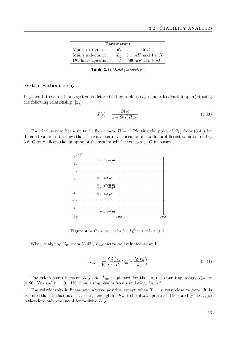
In previous section a linear system model was derived and two transfer functions were obtained.In this section, the obtained transfer functions are used to analyse stability margins of the systemfor different DC link capacitances with and without sampling delay. It will be shown that delayaffects the system considerably, but to understand the influence of a delay the ideal system withouta delay is considered first. Finally, the stability is examined for larger grid side inductance. Thevariables used for the analysis are shown in table 3.2.
35
3.2. STABILITY ANALYSIS
ParametersMains resistance Rg 0.5 ΩMains inductance Lg 0.1 mH and 1 mHDC link capacitance C 500 µF and 5 µF
Table 3.2: Model parameters.
System without delay
In general, the closed loop system is determined by a plant G(s) and a feedback loop H(s) usingthe following relationship, [22]:
T (s) =G(s)
1 +G(s)H(s)(3.43)
The ideal system has a unity feedback loop, H = 1. Plotting the poles of Gvg from (3.41) fordifferent values of C shows that the converter never becomes unstable for different values of C, fig.3.6. C only affects the damping of the system which increases as C increases.
−350 −300 −250−8
−6
−4
−2
0
2
4
6
8x 10
4
← C=1 μF
← C=1 μF
← C=100 μF ← C=100 μF
← C=100 nF
← C=100 nF
Figure 3.6: Converter poles for different values of C.
When analysing Gvd from (3.42), Kvd has to be evaluated as well:
Kvd =1Vs
(2π
Ma
PT qem −
IdcVnωn
)(3.44)
The relationship between Kvd and Tem is plotted for the desired operating range, Tem =[0, 20] Nm and n = [0, 1430] rpm, using results from simulation, fig. 3.7.
The relationship is linear and always positive except when Tem is very close to zero. It isassumed that the load is at least large enough for Kvd to be always positive. The stability of Gvd(s)is therefore only evaluated for positive Kvd.
36

CHAPTER 3. STABILITY ANALYSIS AND DC LINK DIMENSIONING
0 5 10 15 20−0.005
0
0.005
0.01
0.015
0.02
0.025
0.03
0.035
Tem
Kvd
n = 1430 rpmn = 1072.5 rpmn = 715 rpmn = 357.5 rpm
Figure 3.7: Kvd as a function Tem.
Two root locus diagrams are plotted to show the effect of C on Kvd, fig.s 3.8 and 3.9. Thevalue of C has large influence on the damping of the system but the real parts of the poles areunchanged and therefore the stability of the system is not affected. It can be concluded that theDC link capacitor does not affect stability in the ideal system.
−7 −6 −5 −4 −3 −2 −1 0 1
x 104
−4
−3
−2
−1
0
1
2
3
4x 10
4Root Locus
Real Axis
Imag
inar
y A
xis
−7 −6 −5 −4 −3 −2 −1 0 1
x 104
−4
−3
−2
−1
0
1
2
3
4x 10
4Root Locus
Real Axis
Imag
inar
y A
xis
Figure 3.8: Root locus of Gvd with C = 500 µFand Lg = 0.1 mH.
Figure 3.9: Root locus of Gvd with C = 5 µFand Lg = 0.1 mH.
System with delay
But now a sampling delay is included in the feedback loop. The transfer function for a samplingdelay and the value of Td were explained in section 2.2.
H(s) =1− (Tds/2) + (Tds)2/121 + (Tds/2) + (Tds)2/12
(3.45)
The sampling delay was found to be Td = 5 · 10−4 sec.
37

3.2. STABILITY ANALYSIS
The system transfer functions are then:
H(s)Gvg(s) =T 2
d48 s
2 − Td2 s+ 1
CL′gT 2
d48 s
4 +(CL′g
Td2 + CR′g
T 2d
48
)s3 +
(CL′g + CR′g
Td2 + T 2
d48
)s2 +
(CR′g + Td
2
)s+ 1
(3.46)
H(s)Gvd(s) =L′g
T 2d
48 s3 +
(R′g
T 2d
48 − L′gTd2
)s2 +
(L′g −R′g Td
2
)s+R′g
CL′gT 2
d48 s
4 +(CL′g
Td2 + CR′g
T 2d
48
)s3 +
(CL′g + CR′g
Td2 + T 2
d48
)s2 +
(CR′g + Td
2
)s+ 1
(3.47)Fig.s 3.10 and 3.11 show the pole-zero plots of HGvg. As before C has influence on the damping
of the system but does not affect stability.
−5 −4 −3 −2 −1 0 1 2 3 4 5
x 104
−4
−3
−2
−1
0
1
2
3
4x 10
4Pole−Zero Map
Real Axis
Imag
inar
y A
xis
−5 −4 −3 −2 −1 0 1 2 3 4 5
x 104
−4
−3
−2
−1
0
1
2
3
4x 10
4Pole−Zero Map
Real Axis
Imag
inar
y A
xis
Figure 3.10: Pole-zero plot of HGvg with C =500 µF and Lg = 0.1 mH.
Figure 3.11: Pole-zero plot of HGvg with C = 5 µFand Lg = 0.1 mH.
The root-locus diagrams of HGvd in fig.s 3.12 and 3.13 show that both systems become unstablewhen Kvd reaches certain value.
−12 −10 −8 −6 −4 −2 0 2 4 6
x 104
−1
−0.8
−0.6
−0.4
−0.2
0
0.2
0.4
0.6
0.8
1x 10
4Root Locus
Real Axis
Imag
inar
y A
xis
−12 −10 −8 −6 −4 −2 0 2 4 6
x 104
−4
−3
−2
−1
0
1
2
3
4x 10
4Root Locus
Real Axis
Imag
inar
y A
xis
Figure 3.12: Root locus of HGvd with C =500 µF and Lg = 0.1 mH.
Figure 3.13: Root locus of HGvd with C = 5 µFand Lg = 0.1 mH.
But closer look on the root locus diagrams show that the system is marginally stable whenKvd = 1.92 for C = 500 µF and when Kvd = 0.0468 for C = 5 µF , fig.s 3.14 and 3.15. It isexperienced that much higher Kvd is needed to drive the system towards instability for a larger C.
38

CHAPTER 3. STABILITY ANALYSIS AND DC LINK DIMENSIONING
But it is also noticed by examining the range of Kvd within the operating range from fig. 3.7, thatthe unstable region is outside the desired operating range for both C = 500 µF and C = 5 µF .Therefore no unstable conditions in the converter should be encountered within the operating rangefor these parameters.
Root Locus
Real Axis
Imag
inar
y A
xis
−100 −80 −60 −40 −20 0 20 40 60 80 1004600
4610
4620
4630
4640
4650
4660
4670
4680
4690
4700
System: sysGain: 1.92Pole: 0.333 + 4.64e+003iDamping: −7.16e−005Overshoot (%): 100Frequency (rad/sec): 4.64e+003
Root Locus
Real Axis
Imag
inar
y A
xis
−100 −80 −60 −40 −20 0 20 40 60 80 1002.77
2.775
2.78
2.785
2.79
2.795
2.8x 10
4
System: sysGain: 0.0468Pole: 0.278 + 2.79e+004iDamping: −9.98e−006Overshoot (%): 100Frequency (rad/sec): 2.79e+004
Figure 3.14: Zoom on root locus of HGvd withC = 500 µF and Lg = 0.1 mH.
Figure 3.15: Zoom on root locus of HGvd withC = 5 µF and Lg = 0.1 mH.
Increasing the grid side inductance
If the grid side inductance is increased to Lg = 1 mH, the poles move closer to the origin, fig.s 3.16and 3.17.
−12 −10 −8 −6 −4 −2 0 2 4 6
x 104
−1
−0.8
−0.6
−0.4
−0.2
0
0.2
0.4
0.6
0.8
1x 10
4Root Locus
Real Axis
Imag
inar
y A
xis
−12 −10 −8 −6 −4 −2 0 2 4 6
x 104
−1.5
−1
−0.5
0
0.5
1
1.5x 10
4Root Locus
Real Axis
Imag
inar
y A
xis
Figure 3.16: Root locus of HGvd with C =500 µF and Lg = 1 mH.
Figure 3.17: Root locus of HGvd with C = 5 µFand Lg = 1 mH.
For C = 500 µF the system is still always stable within the operating range where the systemis marginally stable for Kvd = 1.74, fig. 3.18. But for C = 5 µF the system is marginally stablefor Kvd = 0.00338 which is unstable within large area of the operating range, fig. 3.19. In fact,the system always becomes unstable within the operating range even when unloaded. This will beexamined with simulation in section 3.4. The unstable condition occurs because whenever the SCIMgoes from standstill to some certain speed the electromagnetic torque increases which increases thegain Kvd and pushes the poles to the right half plane. Despite the fact that the torque settles ratherquickly to value very close to zero it is enough to cause highly unstable fluctuations in the DC linkvoltage where the converter is a much faster system than the SCIM.
39

3.3. DIMENSIONING THE DC LINK CAPACITOR
Root Locus
Real Axis
Imag
inar
y A
xis
−100 −80 −60 −40 −20 0 20 40 60 80 1003600
3650
3700
3750
3800
3850
3900
3950
4000
System: sysGain: 1.74Pole: 0.16 + 3.75e+003iDamping: −4.28e−005Overshoot (%): 100Frequency (rad/sec): 3.75e+003
−100 −80 −60 −40 −20 0 20 40 60 80 1001.005
1.006
1.007
1.008
1.009
1.01
1.011
1.012
1.013
1.014
1.015x 10
4
System: sysGain: 0.00338Pole: 0.698 + 1.01e+004iDamping: −6.91e−005Overshoot (%): 100Frequency (rad/sec): 1.01e+004
Root Locus
Real Axis
Imag
inar
y A
xis
Figure 3.18: Zoom on root locus of HGvd withC = 500 µF and Lg = 1 mH.
Figure 3.19: Zoom on root locus of HGvd withC = 5 µF and Lg = 1 mH.
3.3 Dimensioning the DC link capacitor
As explained in last section the stability of the system is not affected by the DC link capacitor giventhat the system is operated within the desired operating range, . But still there are requirementsfor dimensioning the capacitor.
The natural frequency and damping factor of Gvg and Gvd, from (3.41) and (3.42) are:
ωn =1√L′gC
ξ =1
2ωn
R′gL′g
=R′g2
√C
L′g(3.48)
where L′g = 2Lg, Lg being the grid side inductance.
The DC link voltage generated by the three phase diode rectifier may contain DC and eventriplen harmonics, 6ωg, 12ωg, 18ωg,..., [2]. The capacitor should therefore be selected to not res-onate with these harmonics and especially with 6ωg. This defines the upper margin of the DC linkcapacitor:
C <1
(6ωg)2L′g(3.49)
Here, L′g is not known exactly and has to be estimated. If the grid side inductance Lg is estimatedto be between 1 mH and 0.1 mH, that is 0.2 · 10−3 < L′g < 2 · 10−3, then the lowest upper marginof the capacitor for a grid side frequency ωg = 2π · 50 rad/s, is:
Cmax = 140 µF (3.50)
For the lower margin, the capacitor should be large enough in order not to resonate with theswitching harmonics, which would allow switching harmonics to propagate to the grid side, [5]. Thisdefines the lower margin of the DC link capacitor:
C >1
(ωsw)2L′g(3.51)
The lower limit depends on the switching frequency and can therefore be chosen to some extent.The frequency converter received from Danfoss included a DC link capacitance of C = 5 µF . Thehighest resonance frequency is then fres = 5 kHz. It is therefore necessary to select the switching
40

CHAPTER 3. STABILITY ANALYSIS AND DC LINK DIMENSIONING
frequency so that it does not create switching harmonics in the vicinity of fres.
According to [1], the switching harmonics are determined by the modulation frequency, defined as:
mf =fswf1
(3.52)
f1 being the fundamental frequency of the inverter output voltage.
Theoretically, the voltage harmonics should occur at multiples of mf or as sidebands of loweramplitude, centered at multiples of mf :
fh = (lmf ± k)f1 = lfsw ± kf1 (3.53)
where l defines the multiple of mf and k the sideband.So the switching harmonics normally occur at the switching frequency and at sidebands located
at frequencies ±kf1 from the switching frequency.
If the switching frequency is selected as fsw = 6 kHz then the switching harmonics will oc-cur at frequencies much higher than fres or be of such a low magnitude that they cause negli-able effect. For a DC link capacitance of C = 5 µF and a grid side inductance in the range of0.1 · 10−3 < Lg < 1 · 10−3, the switching frequency is selected to be fsw = 6 kHz.
This will give damping in the range of 0.03 < ξ < 0.1 so large fluctuations in the DC linkvoltage are expected.
3.4 Simulations
Having determined the size of the DC link capacitor and the switching frequency, the systemis simulated to see the intensity of the fluctuations in the DC link. The system is simulated inMatlab/Simulink 7.4.0 (R2007a) with the frequency converter and SCIM modeled using PLECSv2.0.2.
V/f control
Space vector modulation
nrefvabc-ref
qabc PLECScircuit
ωr
Tem
θr
idc
Sample delay
vdc isa
vdc
Figure 3.20: System model.
41
3.4. SIMULATIONS
A block diagram of the simulation setup is shown in fig. 3.20. The SVM has the DC link voltageas input and therefore one sample delay occurs of Td = 0.5 ms as shown in fig. 3.20. The simulationis performed in continuous time.
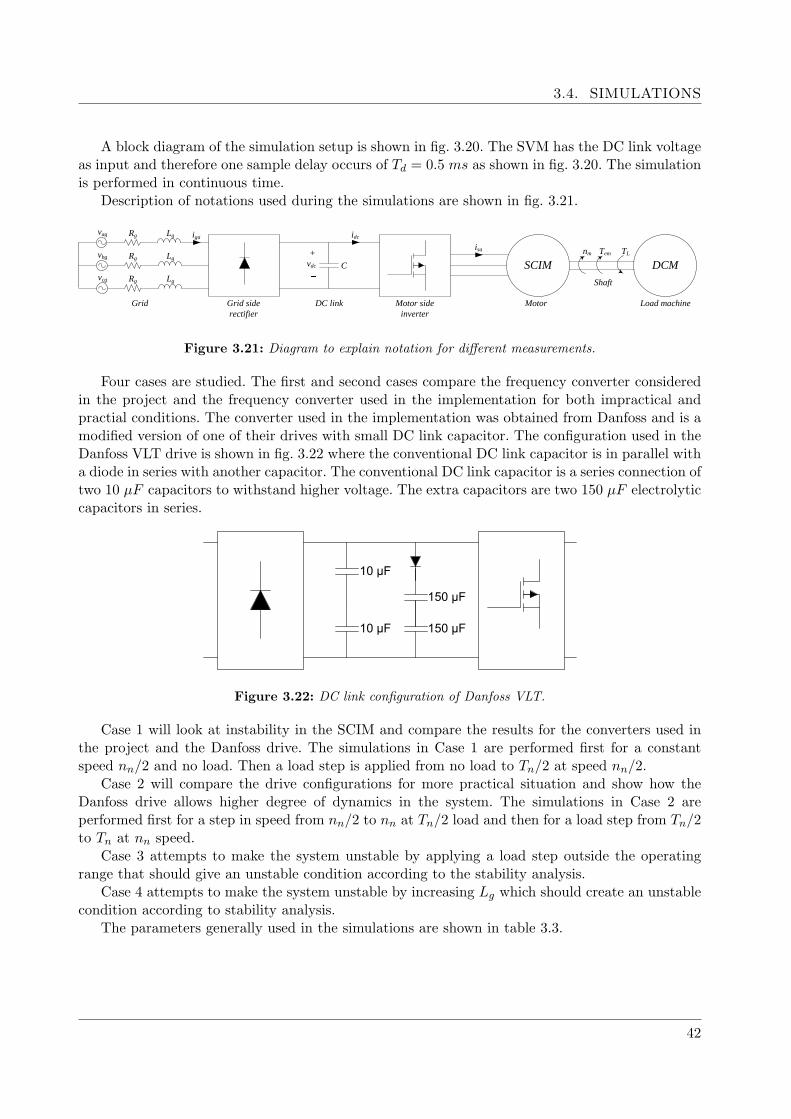
Description of notations used during the simulations are shown in fig. 3.21.
Grid siderectifier
Motor sideinverter
C SCIM DCMnm
Rg Lg
Rg Lg
Rg Lg
vag
vbg
vcg
Motor Load machine
Shaft
Grid DC link
Tem TL
iga idc
vdc
+isa
Figure 3.21: Diagram to explain notation for different measurements.
Four cases are studied. The first and second cases compare the frequency converter consideredin the project and the frequency converter used in the implementation for both impractical andpractial conditions. The converter used in the implementation was obtained from Danfoss and is amodified version of one of their drives with small DC link capacitor. The configuration used in theDanfoss VLT drive is shown in fig. 3.22 where the conventional DC link capacitor is in parallel witha diode in series with another capacitor. The conventional DC link capacitor is a series connection oftwo 10 µF capacitors to withstand higher voltage. The extra capacitors are two 150 µF electrolyticcapacitors in series.
10 μF
10 μF
150 μF
150 μF
Figure 3.22: DC link configuration of Danfoss VLT.
Case 1 will look at instability in the SCIM and compare the results for the converters used inthe project and the Danfoss drive. The simulations in Case 1 are performed first for a constantspeed nn/2 and no load. Then a load step is applied from no load to Tn/2 at speed nn/2.
Case 2 will compare the drive configurations for more practical situation and show how theDanfoss drive allows higher degree of dynamics in the system. The simulations in Case 2 areperformed first for a step in speed from nn/2 to nn at Tn/2 load and then for a load step from Tn/2to Tn at nn speed.
Case 3 attempts to make the system unstable by applying a load step outside the operatingrange that should give an unstable condition according to the stability analysis.
Case 4 attempts to make the system unstable by increasing Lg which should create an unstablecondition according to stability analysis.
The parameters generally used in the simulations are shown in table 3.3.
42
CHAPTER 3. STABILITY ANALYSIS AND DC LINK DIMENSIONING
ParametersMains input voltage Vin 230
√2 Vpeak
Mains resistance Rg 0.5 ΩMains inductance Lg 0.1 mHDC link capacitance C 5 µFStator resistance rs 1.79 ΩStator leakage inductance Lls 7 mHMutual inductance Lm 0.158 HRotor resistance rr 1.8 ΩRotor leakage inductance Llr 0.0144 HPole pairs P 2Motor shaft inertia J 9.57 mNm2
Sample delay Td 0.5 msSwitching frequency fsw 6 kHz
Motor nameplateNominal power Pn 3.0 kWNominal phase voltage Vn 380/
√3 Vrms
Nominal current In 6.9 ArmsNominal frequency fn 50 HzNominal power factor PF 0.77Nominal speed nn 1430 rpmNominal torque Tn 20 Nm
Table 3.3: Model parameters.
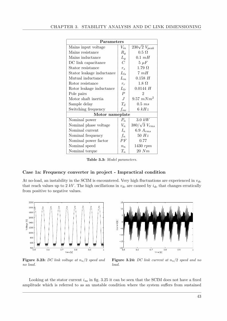
Case 1a: Frequency converter in project - Impractical condition
At no-load, an instability in the SCIM is encountered. Very high fluctuations are experienced in vdcthat reach values up to 2 kV . The high oscillations in vdc are caused by idc that changes erraticallyfrom positive to negative values.
Figure 3.23: DC link voltage at nn/2 speed andno load.
Figure 3.24: DC link current at nn/2 speed and noload.
Looking at the stator current isa in fig. 3.25 it can be seen that the SCIM does not have a fixedamplitude which is referred to as an unstable condition where the system suffers from sustained
43

3.4. SIMULATIONS
oscilliations, [23]. This situation is addressed as being often experienced in a lightly loaded V/HzPWM controlled induction motors, [23] [24] [25]. This instability was not predicted by the stabilityanalysis and could be related to the term that was omitted in the linearized model where it wasdominated by the SCIM. In [24] this unstable behavior is blamed on the stator resistance and istherefore caused by the SCIM which was not part of the stability analysis.
Figure 3.25: Stator current at nn/2 speed and no load.
The sustained oscilliations can well be seen in fig.s 3.26 and 3.27 where the rotor speed nm andthe electromagnetic torque Tem oscilliate heavily in steady state.
Figure 3.26: Rotor speed at nn/2 speed and noload.
Figure 3.27: Electromagnetic torque at nn/2 speedand no load.
44

CHAPTER 3. STABILITY ANALYSIS AND DC LINK DIMENSIONING
But as soon as a load step is applied the oscilliations are damped and the SCIM becomes stable.The oscilliations in vdc decrease to expected variations for a given small DC link capacitor, fig. 3.28.Looking closer at vdc, around 3 periods can be seen during time ∆t = 5 · 10−4 s which shows thatvdc contains harmonics caused by the switching frequency, fig. 3.29.
Figure 3.28: DC link voltage after load step atnn speed.
Figure 3.29: Zoom on DC link voltage after load stepat nn/2 speed.
Fig.s 3.30 and 3.31 show that the currents now have fixed amplitude after the load step hasbeen applied. This is described as a stable condition for the SCIM in [23].
Figure 3.30: DC link current for load step atnn/2 speed.
Figure 3.31: Stator current for load step at nn/2speed.
45

3.4. SIMULATIONS
And from fig.s 3.32 and 3.33 it can be seen that the system stabilizes with the load step as thefluctuations in nm and Tem decrease after the load step is applied.
Figure 3.32: Rotor speed for load step at nn/2speed.
Figure 3.33: Electromagnetic torque for load step atnn/2 speed.
Case 1b: Frequency converter from Danfoss - Impractical condition
Now using the same conditions for the Danfoss drive, vdc is clamped by the extra capacitor bank.But as the charge increases over the extra capacitor bank, the voltage increases, fig. 3.34. idc alsoincreases as the extra capacitor bank charges, fig. 3.35. The configuration can therefore not limitthe sustained voltage fluctuations over a long time, it rather works as a safety which slowly breaks.
Figure 3.34: Danfoss drive. DC link voltage atnn/2 with no load.
Figure 3.35: Danfoss drive. DC link current at nn/2with no load.
The exact same instability behavior in isa is experienced as in Case 1 and it can also be seenhow the fluctuations in nm and Tem are highly linked to vdc where they increase as the fluctuationsin vdc increases, fig.s 3.36 and 3.37.
46

CHAPTER 3. STABILITY ANALYSIS AND DC LINK DIMENSIONING
Figure 3.36: Danfoss drive. Rotor speed at nn/2with no load.
Figure 3.37: Danfoss drive. Electromagnetic torqueat nn/2 with no load.
But as a load step is applied the same situation as in Case 1a is experienced. The SCIM becomesstable and the oscillations decrease. But the ripples in vdc are still considerable because of the smallDC link capacitor, fig. 3.38. The DC link configuration of the Danfoss drive can only help if largeoscillations in vdc are experienced over a short period. Else the same situation is experienced as inCase 1a.
Figure 3.38: Danfoss drive. DC link voltage atnn/2 with Tn/2 load.
Figure 3.39: Danfoss drive. DC link current at nn/2with Tn/2 load.
Case 2a: Frequency converter in project - Practical condition
This case aimes at a more practical condition where simulations are performed for a stable SCIM.At the time of speed change a large overvoltage is observed in vdc, fig. 3.40. This is due to the smallDC link capacitor that does not provide enough damping of the voltage. For this kind of overvoltagethe inverter would normally trip so care has to be taken in implementation to not apply quick speedchanges. Closer look on vdc shows that it contains both harmonics due to the diode rectifier andswitching harmonics, fig. 3.41.
47

3.4. SIMULATIONS
Figure 3.40: DC link voltage for speed step atTn/2 load.
Figure 3.41: Zoom on DC link voltage after speedstep.
The large overvoltage in vdc is caused by large fluctuations in idc, fig. 3.42, and consequently inis, 3.43, which are affected by the large fluctuations in Tem due to the speed step, 3.45.
Figure 3.42: DC link current for speed step atTn/2 load.
Figure 3.43: Stator current for speed step at Tn/2load.
Figure 3.44: Rotor speed for speed step at Tn/2load.
Figure 3.45: Electromagnetic torque for speed step atTn/2 load.
48

CHAPTER 3. STABILITY ANALYSIS AND DC LINK DIMENSIONING
Applying a load step does not affect vdc and idc in the same way as a speed step. No largeovervoltages or overcurrents are experienced in vdc and idc, fig.s 3.46 and 3.48. Looking closer onvdc shows that the amplitude of switching harmonics are increased because a larger current is beingswitched by the inverter, fig. 3.47.
Figure 3.46: DC link voltage for load step at nn
speed.Figure 3.47: Zoom on DC link voltage after load step.
The transition to a higher load is rather smooth and does not cause large overshoot in Temcompared to the overshoot experienced for a speed step.
Figure 3.48: DC link current for load step at nn
speed.Figure 3.49: Stator current for load step at nn speed.
49

3.4. SIMULATIONS
Figure 3.50: Rotor speed for load step at nn
speed.Figure 3.51: Electromagnetic torque for load step atnn speed.
Case 2b: Frequency converter from Danfoss - Practical condition
For a stable SCIM the extra capacitor bank provides extra damping as seen from fig. 3.52, where thefluctuations in vdc are not as dramatic as in Case 2a. This DC link configuration should thereforeallow larger changes in speed compared to the configuration used in Case 2a. Looking closer at vdcthe DC link configuration does not seem to offer more filtering of switching harmonics than theconfiguration in Case 1, fig. 3.53.
Figure 3.52: Danfoss drive. DC link voltage forspeed step at Tn/2 load.
Figure 3.53: Danfoss drive. Zoom on DC link voltageafter speed step.
50

CHAPTER 3. STABILITY ANALYSIS AND DC LINK DIMENSIONING
But idc still jumps to a similar value as in Case 2a where the extra capacitor bank only affectsvdc, fig. 3.54. And the overshoot in Tem also occurs with the Danfoss drive, fig. 3.55.
Figure 3.54: Danfoss drive. DC link current forspeed step at Tn/2 load.
Figure 3.55: Danfoss drive. Electromagnetic torquefor speed step at Tn/2 load.
The load step gives similar results as in Case 2a as the load step did not induce large fluctuationsin vdc.
Case 3: Attempt to create an unstable condition with load step
As was shown in fig. 3.7, the value of Kvd is directly proportional to the electromagnetic torqueTem. If the stability analysis holds, an unstable condition could be created by applying a load steplarge enough. This load step is outside the operating range of the system but can nevertheless beapplied in simulation.
The load step applied is TL = 45 Nm at rated speed nn. This gives Kvd = 0.067 which shouldgive an unstable condition according to stability analysis in section 3.2.
But after the load step is applied at t = 0.5 sec. the system is still stable as seen from vdc infig. 3.56. Due to the load step, idc increases, fig. 3.57. nm decreases as the open loop V/f controldoes not compensate for the added load torque, fig.s 3.58 and 3.59.
Figure 3.56: DC link voltage for estimated un-stable load step.
Figure 3.57: DC link current for estimated un-stable load step.
The reason for this could be because of additional damping which is present in the nonlinearsystem and not included in the linearized model.
51

3.4. SIMULATIONS
Figure 3.58: Rotor speed for estimated unstableload step.
Figure 3.59: Electromagnetic torque for esti-mated unstable load step.
Case 4: Unstable condition for increased Lg
As was shown in section 3.2 the system is unstable if the grid side inductance is increased toLg = 1 mH. Running simulation with no load and rated speed results in increasing fluctuations invdc which is definately unstable for these condtions, fig. 3.60. This finally produces an error in thesimulation when vdc tries to go negative.
Figure 3.60: Unstable DC link voltage for Lg = 1 mH.
As was mentioned in the section 3.2, only a little Tem is needed to make the system unstableand as Tem starts to increase, the grid side current iga starts fluctuating in an uncontrolled fashion,fig.s 3.61 and 3.62.
It can be concluded that the system is unstable for these operating conditions as was predictedby the stability analysis.
52

CHAPTER 3. STABILITY ANALYSIS AND DC LINK DIMENSIONING
Figure 3.61: Electromagnetic torque for unstablecondition.
Figure 3.62: Grid side current for unstable con-dition.
3.5 Summary
Stability analysis of the system were performed in this chapter and stability margins obtained fordifferent parameters. This involved linearization of the system and derivation of small signal modelsto obtain the system transfer functions. The stability of the SCIM was not the focus of this projectand the corresponding term was therefore omitted.
It was shown that the system stability was affected by the DC link capacitor if a samplingdelay was included in the linearized model. The system was stable within the operating range forthe analysed capacitor sizes but a load step outside the operating range should give an unstablecondition according to the stability analysis. This was disproven by simulation which could bebecause the nonlinear model contains some dampings that are not included in the linearized model.
It was also shown that the grid side parameters have large effect on system stability. The systemwas unstable for a DC link capacitor of 5 µF and a grid side inductance of 1 mH. This instabilitybehavior was then tested and proven by simulation.
53

Chapter 4
Implementation
Description of test setup and technical information relevant for the implementation are provided inthis chapter along with experimental results.
4.1 Test setup
To observe the problems arising because of the small DC link capacitor the system is implemented ona test bench. This requires a digital signal controller (DSC) to control the frequency converter usingthe DC link voltage as feedback. Speed reference and DC link voltage are the only variables neededto control the SCIM employing V/f control and space vector modulation. Following subsectionsgive a small description of the components used in the test setup.
DSC
The DSC consist of a digital signal processor (DSP) and a great deal of microcontrollers that worktogether creating a low-cost and powerful solution for many embedded applications.
The DSC used in the project is the TMS320F2812 from Texas Instruments. It provides a highoperating clock frequency of 150 MHz, 32-bit processing capabilities and a comfortable floatingto fixed-point conversion through the IQ Math library which also includes dozens of arithmetic,trigonometric and numberical conversion functions, [26].
During the experimental testing, two important capabilities of the DSC are used, PWM gener-ation and ADC conversion.
The PWM generation occurs through the use of general-purpose timers and full-compare unitswhich are part of the event-manager modules on the DSC, [27]. There is also a possiblity for pro-gramming a deadband but it is not used where it is integrated into the Danfoss VLT. The switchingfrequency used is fsw = 6 kHz.
The analog-to-digital conversion occurs through a 12-bit pipelined analog-to-digital converter(ADC) module. The main analog ciruits in the ADC module are the front-end analog multiplexers,sample and hold circuits and the conversion core. The ADC module consists of two independent 8channel modules which can be cascaded to form a 16 channel module. Each 8 channel module hasits sperate analog multiplexer and sample and hold circuit but only one converter core is present
54
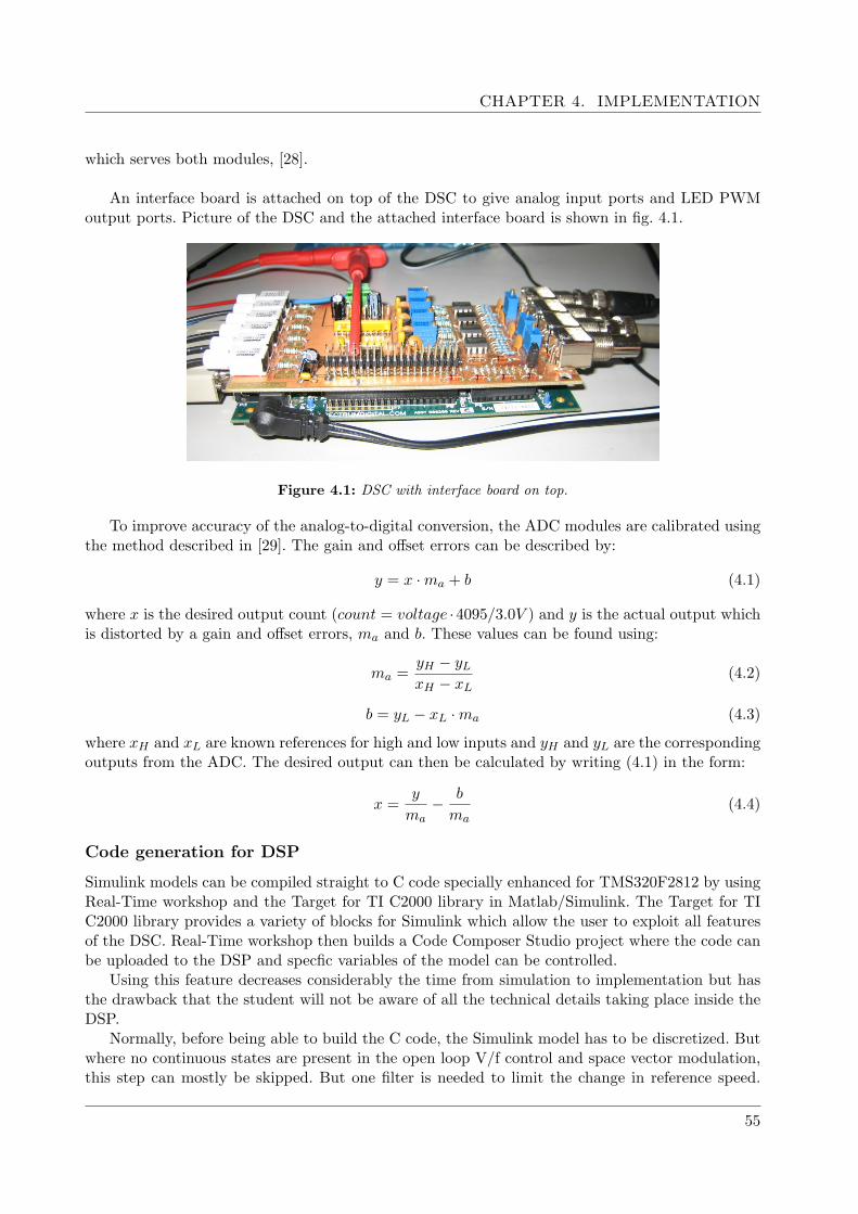
CHAPTER 4. IMPLEMENTATION
which serves both modules, [28].
An interface board is attached on top of the DSC to give analog input ports and LED PWMoutput ports. Picture of the DSC and the attached interface board is shown in fig. 4.1.
Figure 4.1: DSC with interface board on top.
To improve accuracy of the analog-to-digital conversion, the ADC modules are calibrated usingthe method described in [29]. The gain and offset errors can be described by:
y = x ·ma + b (4.1)
where x is the desired output count (count = voltage ·4095/3.0V ) and y is the actual output whichis distorted by a gain and offset errors, ma and b. These values can be found using:
ma =yH − yLxH − xL
(4.2)
b = yL − xL ·ma (4.3)
where xH and xL are known references for high and low inputs and yH and yL are the correspondingoutputs from the ADC. The desired output can then be calculated by writing (4.1) in the form:
x =y
ma− b
ma(4.4)
Code generation for DSP
Simulink models can be compiled straight to C code specially enhanced for TMS320F2812 by usingReal-Time workshop and the Target for TI C2000 library in Matlab/Simulink. The Target for TIC2000 library provides a variety of blocks for Simulink which allow the user to exploit all featuresof the DSC. Real-Time workshop then builds a Code Composer Studio project where the code canbe uploaded to the DSP and specfic variables of the model can be controlled.
Using this feature decreases considerably the time from simulation to implementation but hasthe drawback that the student will not be aware of all the technical details taking place inside theDSP.
Normally, before being able to build the C code, the Simulink model has to be discretized. Butwhere no continuous states are present in the open loop V/f control and space vector modulation,this step can mostly be skipped. But one filter is needed to limit the change in reference speed.
55

4.1. TEST SETUP
A quick change in speed generates large overvoltages and overcurrents due to the small DC linkcapacitor, this can cause the frequency converter to trip. The filter is a 1st order with cutofffrequency fcut = 0.1 Hz. This filter is discretized using the trapezoidal method, [30]:(
1s
0.2π + 1
)s= 2
Ts
z−1z+1
=z + 1
19100z − 19098(4.5)
where Ts is the sampling period, Ts = (6 · 103)−1 sec.
A screenshot of the Simulink model to be compiled to the DSP is shown in fig. 4.2. A ratetransition is needed because there is a difference in clock frequency between the ”Vdc” signaland the SVM function. The ”Vdc” signal is at clock frequency equal to the sampling frequency,fs = 6 kHz while the SVM function is working at the DSP clock frequency, 150 MHz. Buffersare needed to view the signals graphically in Code Composer Studio. The variables ”duty1” and”n ref” are then the corresponding memory addresses to the data.
speedref
300
V/f control
n_ref v _abc
Terminator 5
Terminator 4
Terminator 3
Terminator 2
Terminator 1
Terminator
S-Function Builder 1
svm_sfunction_dsp
va_ref
vb_ref
vc_ref
V_dc
sw_abc
Rate Transition
PWM1
C281x
PWM
W2
PWM
C281x
PWM
W1W2W3
Initialize parameters
Gain 6
1
Gain 5
-K-
Gain 4
-K-
Gain 3
-K-
Gain 2
-K-
Gain 1
-K-
Gain
100
F2812 eZdsp
Enable
0
DiscreteTransfer Fcn
z+1
19100 z-19098
CalOffset3
-1.12
CalOffset2
20.79
CalOffset1
-C-
CalOffset
46.67
CalGain 3
-K-
CalGain 2
-K-
CalGain 1
-K-
CalGain
-K-
Buffer1
Buffer
ADC
C281x
ADC
A0
A1
A2
A3
duty 1
n_ref
Current 1
Current 2
speed
Vdc
Figure 4.2: Screenshot of Simulink model for DSP.
SCIM
The motor in the test setup is a three phase squirrel cage induction motor from ABB motors. Ithas a rated input voltage of 380 Vrms and maximum voltage of 420 Vrms when Y-connected. Ratedcurrent is 6.9 Arms and rated power 3 kW . Picture of the SCIM and the load machine is shown infig. 4.3. Motor nameplate can be seen in appendix C.
56

CHAPTER 4. IMPLEMENTATION
Figure 4.3: Load machine (left) and SCIM (right) in the test setup.
Load machine
The load machine is a 3.3 kW DC motor (DCM) from Thrige-Titan A/s. It has seperately excitedfield windings with nominal field current of if = 0.7 A. Nameplate of motor can be viewed inappendix C.
In order to load the SCIM with the DCM the armature windings of the DCM have to beconnected to a variable resistance while feeding the field windings with the nominal field current.Holding the field current constant ensures a constant direct axis field Φd and the electromechanicaltorque of the DCM Tdc is only controlled by the armature current iarm as shown in (4.6), [31].
Tdc = KaΦdiarm (4.6)
where Ka is a constant determined by the design of the motor.From the data given on the DCM, it should generate a load torque of Tdc = 20 Nm for
iarm = 9.7 A while holding if = 0.7 A. As iarm is directly proportional to Tdc the load torque cannow be controlled with iarm by varying the variable resistance. Fig. 4.4 explains the installation ofthe load machine.
if
if
iarm
d
Figure 4.4: Installation of load machine.
Danfoss VLT
The Danfoss frequency converter used in the test setup is a modified version of the 2.2kW FC-302VLT. The modification is associated with the DC link configuration which has been changed to
57

4.2. EXPERIMENTAL RESULTS
the one that was explained in fig. 3.22. The interface board attached to the VLT offers inputs forexternal PWM waveforms and configuration of deadband. Deadband is set to 2 µs. Picture of theVLT with attached interface board is shown in fig. 4.5.
Figure 4.5: Danfoss VLT with attached interface board.
4.2 Experimental results
To show how a highly fluctuating feedback signal affects the systems steady state behavior, experi-mental tests were performed for three cases of scaling factor for the SVM, DC link voltage feedback,filtered DC link voltage feedback and no feedback where scaling factor was set as constant. In allcases, open loop V/f control was used as a speed control strategy and SVM for modulation. Fig.4.6 explains the three different cases by block diagrams. Screenshots of plots from oscilloscopes areavailable in appendix B.
ADCDiscretefilter
SVM
vabc-ref
vdc Scaling factor
Reference voltages
dabc
ADC
SVM
vabc-ref
vdc Scaling factor
Reference voltages
dabc
Constant
SVM
vabc-ref
vdc Scaling factor
Reference voltages
dabc
Case 1: vdc feedback Case 2: Filtered vdc feedback Case 3: Constant vdc
Figure 4.6: Graphical explanation of different scaling factors for each case.
Case 1a: vdc feedback - No load
Driving the SCIM with no load at rated speed, nn = 1430 rpm results in relatively low stator currentas seen in fig. 4.8. The stator current has harmonics of 5th order that are caused by deadtime. TheDC link voltage is fluctuating because of the low DC link capacitance, fig. 4.7. The instabilitybehavior encountered in simulation in section 3.4 is not experienced in the implementation.
Looking closer on the DC link voltage, it can be seen that it contains both ripple caused by thediode rectifier and ripple caused by switching harmonics, fig.s 4.9 and 4.10.
The rotor speed contains some high frequency ripples of low amplitude but is rather constant.
58

CHAPTER 4. IMPLEMENTATION
Figure 4.7: vdc feedback. DC link voltage at noload, rated speed.
Figure 4.8: vdc feedback. Stator current at noload, rated speed.
Figure 4.9: vdc feedback. Ripple caused by dioderectifier at no load, rated speed.
Figure 4.10: vdc feedback. Ripple caused byswitching harmonics at no load, rated speed.
Figure 4.11: vdc feedback. Rotor speed at no load, rated speed.
59

4.2. EXPERIMENTAL RESULTS
Case 1b: vdc feedback - Full load
Loading the SCIM with rated load, Tn = 20 Nm, increases the stator current as seen in fig. 4.13.The DC link voltage now has switching harmonics of higher amplitude as higher current is beingswitched by the inverter, fig. 4.12. This complies with simulations in section 3.4.
Figure 4.12: vdc feedback. DC link voltage at fullload, rated speed.
Figure 4.13: vdc feedback. Stator current at fullload, rated speed.
The rotor speed now contains very large ripples, fig. 4.14. Looking at a the rotor speed over alarger period it can be seen that these ripples occur rather periodically, fig. 4.15.
Figure 4.14: vdc feedback. Rotor speed at fullload, rated speed.
Figure 4.15: vdc feedback. Rotor speed from alarger time frame at full load, rated speed.
Case 2: Filtered vdc feedback
As mentioned in Case 1a the DC link voltage contains ripples caused by the switching frequencyharmonics. In this case these harmonics are filtered with a 1st order filter with cut-off frequencyfc = 500 Hz before being used as a scaling factor for the SVM. The discretized form of the filteris: (
1s
2π·500 + 1
)s= 2
Ts
z−1z+1
=3142z + 314215142z − 8858
(4.7)
with Ts = (6 · 103)−1 sec.This gives results similar to Case 1 which implies that the ripples in rotor speed are not caused
by the switching harmonics in the SVM scaling factor. The ripples are more likely caused by thedelay between the scaling factor used in the SVM and the actual DC link voltage.
60

CHAPTER 4. IMPLEMENTATION
Figure 4.16: Filtered vdc feedback. DC link volt-age at no load, rated speed.
Figure 4.17: Filtered vdc feedback. Stator currentat no load, rated speed.
Figure 4.18: Filtered vdc feedback. Rotor speed at no load, rated speed.
Figure 4.19: Filtered vdc feedback. DC link volt-age at full load, rated speed.
Figure 4.20: Filtered vdc feedback. Stator currentat full load, rated speed.
61

4.2. EXPERIMENTAL RESULTS
Figure 4.21: Filtered vdc feedback. Rotor speed at full load, rated speed.
Case 3: Constant vdc - Full load
The feedback is replaced by a constant which is the calculated average value of the DC link voltage,[5]:
vdc(AV G) = 3√
3Vin/π (4.8)
where Vin = 380√
2/√
3 is the peak of the grid side voltage.This is actually similar to Case 2 where the constant can be thought of as a filter with even
lower passband than in Case 2 which rejects the harmonics caused by the diode rectifier. The resultsare very similar to Cases 1 and 2.
Figure 4.22: Constant vdc. DC link voltage at fullload, rated speed.
Figure 4.23: Constant vdc. Stator current at fullload, rated speed.
62

CHAPTER 4. IMPLEMENTATION
Figure 4.24: Constant vdc. Rotor speed at full load, rated speed.
4.3 Summary
This chapter included a description of each component in the test setup and covered importanttechnical details regarding the implementation followed by a section about experimental results.
Experiments were performed for different scaling factors for the SVM to see if that affectedthe performance of the drive for different load torques. All cases gave similar results. The DC linkvoltage contained larger harmonics for larger load due to switching of higher currents. The rotorspeed had large spikes at full load which was not encountered in simulations. It was also observedthat the stator currents suffered from 5th harmonic content which was caused by deadtime.
63

Chapter 5
Conclusion
This project has analysed stability margin of a frequency converter equipped with a diode rectiferand a small DC link capacitor. This topic is mainly of concern in low cost drives where a dioderectifier and smaller DC link capacitor can decrease the cost of the drive considerably. A DC linkcapacitor under certain size opens the possibilty for replacing the expensive, bulky and short livingelectrolytic capacitor for a MPPT capacitor which is cheaper and has longer lifetime and lowerlosses. But a small DC link capacitor does not provide a suitable filtering of the harmonics causedby the diode rectifier, which results in a highly fluctuating DC link voltage. This introduces largetorque ripple and the drive becomes very sensitive for quick changes in speed where this createslarge DC link overvoltage and can cause the frequency converter to trip. These types of converterscan therefore only be used in low performance drives.
The first step in analysing the system was to build a model of all components of the systemfor simulations in Matlab/Simulink 7.4.0 (R2007a). Models of every component were explained inchapter 2 except for the diode rectifier and DC link models, which were obtained from supervisor.Many attempts were made to build a satisfying diode rectifier model but as the project time waslimited the supervisor provided a model. With the complete model, a sensorless V/f control strategywas simulated. It was found that it gave improved speed accuracy over the open loop V/f controlbut introduced more ripples. Filters could be added to reduce the ripples which would in turnreduce the dynamic capabilities of the drive. But where the drive is considered as low performancethis would not be of concern.
The frequency converter was then linearized in chapter 3 and three transfer functions wereobtained. One of these transfer functions was omitted because it was dominated by the SCIMwhich was not of concern in this project. The linearized model of the frequency converter was thenformed by two inputs, the operating frequency of the motor and grid side input voltage, whichaffected the output, the DC link voltage. This model was found to be always stable for the idealcase where no delay was present in the system. But when a sampling delay was included, unstableconditions were encountered but they were outside the operating range of the SCIM. Increasingthe grid side inductance affected the stability margin considerably and the system could be madeunstable for all operating conditions. An attempt was made to verify the stability margins of thesystem by simulation in Matlab/Simulink. Now, PLECS v2.0.2 was used to model the frequencyconverter and SCIM to speed up simulations and allow the DC link configuration of the Danfossfrequency converter used in implentation to be simulated. The system could not be made unstableby applying a load step outside the operating range which should create an unstable conditionaccording to the stability analysis. This could have been caused by additional damping that ispresent in the nonlinear model but not included in the linearized model. The torque step could
64
CHAPTER 5. CONCLUSION
not be increased much further where the SCIM could not maintain speed for much higher loadtorques in the simulation. But an unstable condition could be simulated by increasing the grid sideinductance. This condition was preditcted by the stability analysis.
Chapter 4 of the report was devoted to implementation and experimental results. Componentsof the test setup were described and technical details required for the implementation were coveredas well. The open loop V/f control and SVM were implemented on a DSP using Real-Time workshopand Target for TI C2000 library in Matlab/Simulink. The SCIM was driven by a modified DanfossVLT with small DC link capacitor and an extra capacitor bank which worked as a short-termovervoltage protection. A DCM was used as a load machine. Testings were made for differentscaling factors for the SVM and experimental results were obtained. The different scaling factorsdid not have any visible effect on the performance of the system. The sensorless V/f control strategycould not be implemented during the project period due to time constraints.
65
Chapter 6
Future work
• Further evaluation of the effect of grid side parameters Rg and Lg.
• Evaluation of the effect of the squirrel cage induction motor on stability by including the termthat was omitted from the stability analysis.
• Implementation of sensorless V/f control.
• Design of controller to compensate for the voltage fluctuations.
66

BIBLIOGRAPHY
Bibliography
[1] N. Mohan, T. M. Undeland, and W. P. Robbins, Power electronics, Converters, Applicationsand Design. John Wiley and sons, media enhanced 3rd ed., 2003.
[2] R. W. Erickson and D. Maksimovic, Fundamentals of Power Electronics. Springer Sci-ence+Buisness Media, 2nd ed., 2001.
[3] A. M. Hava, R. J. Kerkman, and T. A. Lipo, “Simple analytical and graphical methods forcarrier-based PWM-VSI drives,” IEEE Transactions on power electronics, vol. 14, January2005.
[4] V. M. Cardenas, S. Horta, and R. Echavarrıa, “Elimination of dead time effects in three phaseinverters,” IEEE, 1996.
[5] M. Hinkkanen and J. Luomi, “Induction motor drives equipped with diode rectifier and smallDC-link capacitance,” IEEE Transactions on Industrial Electronics, January 2008.
[6] H. Saren, O. Pyrhonen, J. Luukko, O. Laakkonen, and K. Rauma, “Verification of frequencyconverter with small DC-link capacitor,” EPE 2005 Dresden, 2005.
[7] K. Kretschmar and H.-P. Nee, “An AC converter with a small DC link capacitor for a 15kWpermanent magnet synchronous integral motor,” Power Electronics and Variable Speed Drives,21-23 September 1998, Conference Publication No. 456, IEEE, 1998.
[8] H. Saren, O. Pyrhonen, K. Rauma, and O. Laakonen, “Overmodulation in voltage sourceinverter with small DC-link capacitor,” IEEE, 2005.
[9] H. Saren, K. Rauma, and O. Pyrhonen, “DTC driven single phase fed voltage source inverterwith small DC-link capacitor,” IEEE ISIE, June 2005.
[10] H. Mosskull, “Stabilization of an induction motor drive with resonant input filter,” EPE 2005Dresden, 2005.
[11] H. W. Van Der Broeck, H.-C. Skudelny, and G. V. Stanke, “Analysis and realization of apulsewidth modulator based on space vectors,” IEEE Transactions on Industry Applications,vol. 24, January/February 1988.
[12] J. Holtz, “Pulsewidth modulation for electronic power conversion,” Proceedings of the IEEE,vol. 82, August 1994.
[13] G. F. Franklin, J. D. Powell, and A. Emami-Naeini, Feedback Control of Dynamic Systems.Pearson Prenitce Hall, 5th ed., 2006.
67

BIBLIOGRAPHY
[14] G. R. Slemon, “Modelling of induction machines for electric drives,” IEEE Transactions onIndustry Applications, vol. 25, November/December 1989.
[15] D. W. Novotny and T. A. Lipo, Vector Control and Dynamics of AC Drives. Oxford publica-tions, 1st ed., 1996.
[16] P. C. Krause, O. Wasynczuk, and S. D. Sudhoff, Analysis of Electric Machinery and DriveSystems. Wiley-Interscience, 2nd ed., 2002.
[17] C.-C. Wang and C.-H. Fang, “Sensorless scalar-controlled induction motor drives with modifiedflux observer,” IEEE Transactions on Energy Conversion, vol. 18, June 2003.
[18] H. Luo, Q. Wang, X. Deng, and S. Wan, “A novel V/f scalar controlled induction motor driveswith compensation based on decoupled stator current,” IEEE, 2006.
[19] J. Hu and B. Wu, “New integration algorithms for estimating motor flux over a wide speedrange,” IEEE Transactions on Power Electronics, vol. 13, September 1998.
[20] A. Munoz-Garcıa, T. A. Lipo, and D. W. Novotny, “A new induction motor V/f controlmethod capable of high-performance regulation at low speed,” IEEE Transactions on IndustryApplications, vol. 34, July/August 1998.
[21] M. P. Kazmierkowski, R. Krishnan, and F. Blaabjerg, Control in Power Electronics. AcademicPress, 1st ed., 2002.
[22] C. L. Phillips and R. D. Harbor, Feedback Control Systems. Prentice Hall, 4th ed., 2000.
[23] Z. Ma, T. Zheng, and F. Lin, “Stability improvement of V/Hz controlled PWM inverter-fedinduction motors drives,” IEEE, 2006.
[24] R. Ueda, T. Sonoda, K. Koga, and M. Ichikawa, “Stability analysis in induction motor driven byV/f controlled general-purpose inverter,” IEEE Transactions on Industry Applications, vol. 28,March/April 1992.
[25] J.-H. Jung, G.-Y. Jeong, and B.-H. Kwon, “Stability improvement of V/f-controlled inductionmotor drive systems by a dynamic current compensator,” IEEE Transactions on IndustrialElectronics, vol. 51, August 2004.
[26] TMS320C2000 Digital Signal Controllers Brochure (Rev. B), July 2007. Material from TexasInstruments website, http://www.ti.com/litv/pdf/sprb176b.
[27] TMS320x281x Event Manager (EV) Reference Guide (Rev. E), June 2007. Material fromTexas Instruments website, http://www.ti.com/litv/pdf/spru065e.
[28] TMS320x281x Analog-to-Digital Converter (ADC) Reference Guide (Rev. D), July 2005. Ma-terial from Texas Instruments website, http://www.ti.com/litv/pdf/spru060d.
[29] TMS320F2810, TMS320F2811, TMS320F2812 ADC Calibration (Rev. A), November 2004.Material from Texas Instruments website, http://www.ti.com/litv/pdf/spra989a.
[30] G. F. Franklin, J. D. Powell, and M. Workman, Digital Control of Dynamic Systems. AddisonWesley, 3rd ed., 1998.
[31] A. Fitzgerald, C. K. Jr., and S. D. Umans, Electric Machinery. McGraw-Hill, 6th ed., 2003.
68

APPENDIX A. SVM S-FUNCTION CODE
Appendix A
SVM S-function code
double va,vb,vc,v0,va_n,vb_n,vc_n;double d1,d2,d3;
//Normalize reference voltagesva_n = va_ref[0]/(0.5*V_dc[0]);vb_n = vb_ref[0]/(0.5*V_dc[0]);vc_n = vc_ref[0]/(0.5*V_dc[0]);
//Find the absolute valuesva=fabs(va_n);vb=fabs(vb_n);vc=fabs(vc_n);
//Find the lowest of va,vb,vc//Zero sequence signal: v0 = 0.5*min(va,vb,vc)if(va<vb)
if(va<vc)
v0=0.5*va_n;else
v0=0.5*vc_n;
else
if(vb<vc)
v0=0.5*vb_n;
69

else
v0=0.5*vc_n;
//Duty cyclesd1 = va_n+v0;d2 = vb_n+v0;d3 = vc_n+v0;
//Saturationif(d1>1)d1=1;if(d2>1)d2=1;if(d3>1)d3=1;if(d1<-1)d1=-1;if(d2<-1)d2=-1;if(d3<-1)d3=-1;
//Outputssw_abc[0] = d1/2+0.5;sw_abc[1] = d2/2+0.5;sw_abc[2] = d3/2+0.5;
70

APPENDIX B. SCREENSHOTS FROM OSCILLOSCOPE
Appendix B
Screenshots from oscilloscope
Following appendix shows screenshots taken from the oscillioscope when experimental data wascaptured. Conversion ratios to convert voltage unit on the oscilloscopes y-axis to meaningful unitsare shown in table B.1.
Unit description Conversion ratioDC link voltage 500V 2/VStator current 2000/150A/VRotor speed 800rpm/V
Table B.1: Acquisition ratios.
Case 1a: vdc feedback - No load
Figure B.1: vdc feedback. DC link voltage at noload, rated speed.
Figure B.2: vdc feedback. Stator current at noload, rated speed.
71

Figure B.3: vdc feedback. Rotor speed at full load, rated speed.
Case 1b: vdc feedback - Full load
Figure B.4: vdc feedback. DC link voltage at fullload, rated speed.
Figure B.5: vdc feedback. Stator current at fullload, rated speed.
72

APPENDIX B. SCREENSHOTS FROM OSCILLOSCOPE
Figure B.6: vdc feedback. Rotor speed at full load, rated speed.
Case 2: Filtered vdc feedback
Figure B.7: Filtered vdc feedback. DC link voltageat no load, rated speed.
Figure B.8: Filtered vdc feedback. Stator currentat no load, rated speed.
73

Figure B.9: Filtered vdc feedback. Rotor speed at no load, rated speed.
Figure B.10: Filtered vdc feedback. DC link volt-age at full load, rated speed.
Figure B.11: Filtered vdc feedback. Stator currentat full load, rated speed.
74

APPENDIX B. SCREENSHOTS FROM OSCILLOSCOPE
Figure B.12: Filtered vdc feedback. Rotor speed at full load, rated speed.
Case 3: Constant vdc - Full load
Figure B.13: Constant vdc. DC link voltage atfull load, rated speed.
Figure B.14: Constant vdc. Stator current at fullload, rated speed.
75
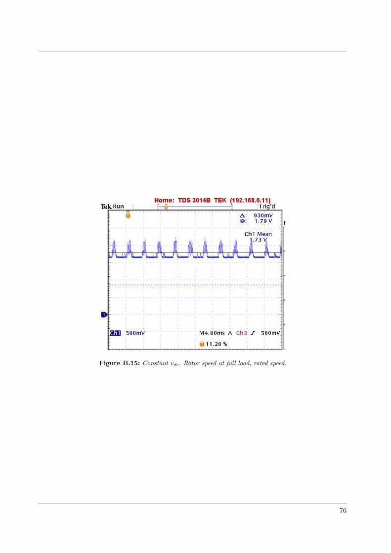
Figure B.15: Constant vdc. Rotor speed at full load, rated speed.
76

APPENDIX C. MOTOR NAMEPLATES
Appendix C
Motor nameplates
Tables C.1 and C.2 nameplates of the SCIM and DCM used in the project.
Motor nameplateABB Motors - MT100LB28-4 MK110023-5
Nominal power Pn 3.0 kWNominal phase voltage Vn 380/
√3 Vrms
Maximum phase voltage Vn(max) 420/√
3 VrmsNominal current In 6.9 ArmsNominal frequency fn 50 HzNominal power factor PF 0.77Nominal speed nn 1430 rpmNominal torque Tn 20 Nm
Table C.1: SCIM nameplate.
Motor nameplateThrige-Titan A/s - Motor shunt - CLASS F
LAK132 - No. 2247266-8249Nominal power Pn 3.3 kWNominal armature voltage Varm 400 VNominal armature current Iarm 9.7 ANominal field voltage Vf 220 VNominal field current If 0.7 ANominal speed nn 1560 rpmNominal torque (If = 0.7 A, Iarm = 9.7 A) Tn 20 Nm
Table C.2: DCM nameplate.
77

Appendix D
Contents of CD-ROM
The enclosed CD-ROM contains the following:
• Root of CD-ROM
– This folder contains the report in pdf format.
• References
– This folder contains the papers in the Bibliography.
• Report
– This folder contains the latex source files of the report and pictures.
• Simulations
– This folder contains the Simulink models used in simulations.
• Implementation
– This folder contains the Simulink models used in implementation, documents related tothe DSP and pictures of the setup.
• Other stuff
– This folder contains other stuff that was used during the project period, datasheets,m-files, models etc.
78


![Pratham Annual Report2008[1]](https://static.fdocuments.us/doc/165x107/577d34fa1a28ab3a6b8f4c19/pratham-annual-report20081.jpg)


