
AN96072 TDA6107Q-N1 v deo output amplifierapplication-notes.digchip.com/004/4-7934.pdf · ·...
37
APPLICATION NOTE Application and product Description of the TDA6107Q-N1 video output amplifier AN96072
Transcript of AN96072 TDA6107Q-N1 v deo output amplifierapplication-notes.digchip.com/004/4-7934.pdf · ·...

APPLICATION NOTE
Application and productDescription of the TDA6107Q-N1
video output amplifierAN96072
Philips Semiconductors__________________________________________________________________TDA6107Q-N1 Application NoteVideo output amplifier AN96072
-2-
Abstract
This report gives the description of the TDA6107Q video output amplifier together with applicationaspects
© Philips Electronics N.V. 1997
All rights are reserved. Reproduction in whole or in part is prohibited without the prior written consent of thecopyright owner. The information presented in this document does not form part of any quotation or contract, isbelieved to be accurate and reliable and may be changed without notice. No liability will be accepted by the publisherfor any consequence of its use. Publication thereof does not convey nor imply any license under patent- or otherindustrial or intellectual property rights.
Philips Semiconductors__________________________________________________________________TDA6107Q-N1 Application NoteVideo output amplifier AN96072
-3-
Application and productDescription of the TDA6107Q-N1
video output amplifierAN96072
Author(s):
E.H. SchutteDesign & Application Video Group, Consumer IC's Nijmegen,
The Netherlands
Keywords
Video output amplifierBandwidthDissipationFlash-over
Black current stabilization
Date: February, 1997
Philips Semiconductors__________________________________________________________________TDA6107Q-N1 Application NoteVideo output amplifier AN96072
-4-
Summary
This note gives the device description of the TDA6107Q-N1 RGB video output amplifier and provides the user with basic hints to obtain an optimal performance in the application.The TDA6107Q-N1 includes three video output amplifiers in a SIL 9 MP (Single InLine 9 pins Medium Power) package SOT111BE, using high-voltage DMOS technology, and is intended to drive the three cathodes of a colour picture tube.Furthermore the device is provided with a black current measurement output for automatic black current stabilsation (ABS).In contrast to previous types of DMOS video output amplifiers, the external resistors(Rf,Ri and Ra) are integrated, so the gain is fixed which saves 9 resistors.To obtain maximum performance, the amplifier should be used with black-currentcontrol. In that case, there are no alignments any more on the CRT board, because of the automatic black current stabilisation and because the white point adjustment can be done in the TDA837X/TDA884X via I2C.

Philips Semiconductors__________________________________________________________________TDA6107Q-N1 Application NoteVideo output amplifier AN96072
-5-
TABLE OF CONTENTS:
1.0 INTRODUCTION............................................................................................. 72.0 QUICK REFERENCE DATA........................................................................... 83.0 CIRCUIT DESCRIPTION................................................................................ 10
- 3.1 Block diagram description................................................................ 10- 3.2 Functional pin description................................................................. 11- 3.3 Internal pin configuration.................................................................... 12- 3.4 Protection circuits............................................................................... 12
4.0 DESIGN CONSIDERATIONS......................................................................... 13- 4.1 Basic aspects amplifier part............................................................ 13- 4.2 Voltage gain....................................................................................... 13- 4.3 DC to DC transfer............................................................................... 14- 4.4Stability. ............................................................................................... 14- 4.5 Black current measurement output..................................................... 15- 4.6 Flash-over protection.......................................................................... 15- 4.7 Thermal protection............................................................................. 15
5.0 EXTERNAL COMPONENTS CALCULATION................................................. 16- 5.1 Decoupling......................................................................................... 16
6.0 DISSIPATION & HEATSINK CALCULATION.................................................. 17- 6.1 Static and dynamic dissipation........................................................... 17- 6.2 A more practical approach regarding dissipation............................. 17- 6.3 Heatsink calculation........................................................................... 18
7.0 CIRCUIT APPLICATION & APPLICATION HINTS........................................ 19• Application diagram of the TDA6107Q-N1............................................... 28• Partlist...................................................................................................... 29• Evaluation board layout & component view.............................................. 30- 7.1 Design-in sequence of the TDA6107Q-N1......................................... 19- 7.2 Printed circuit board........................................................................... 19- 7.3 Switch off behaviour........................................................................... 20- 7.4 Flash- over protection......................................................................... 21- 7.5 Black- current stabilisation................................................................24
8.0 PERFORMANCE EVALUATION..................................................................... 25- 8.1 Bandwidth........................................................................................... 25- 8.2 Cross-talk........................................................................................... 25- 8.3 Rise and Fall time............................................................................... 26- 8.4 Flash test............................................................................................ 26
9.0 REFERENCES............................................................................................... 2710.0 APPENDIX
- Imperfections of the TDA6107Q-N1......................................................… 37

Philips Semiconductors__________________________________________________________________TDA6107Q-N1 Application NoteVideo output amplifier AN96072
-6-
READ ME
The TDA6107Q-N1 does not meet the original specification target.For a good flash immunity with the TDA6107Q-N1 it is necessary to apply an externalprotection circuit (resistor & flash diode) for each channel.The N2 version will be improved regarding flash robustness, in that case it is allowed toeliminate these extra components.For more detailed information concerning imperfections of N1 version, see appendix.Never the less, by using the application hints given in this report a well performing andattractive low-cost video output stage can be realised with the TDA6107Q -N1.

Philips Semiconductors__________________________________________________________________TDA6107Q-N1 Application NoteVideo output amplifier AN96072
-7-
1.0 INTRODUCTION
The aim of this application note is to describe the basic operation of the TDA6107Q-N1 RGB triple video output amplifier and provide the user with basic hints to realise an optimal performance in the application.The TDA6107Q-N1 includes three video output amplifiers in a SIL 9 MP (Single InLine 9 pins Medium Power) package SOT111BE, using high-voltage DMOS technology, and is intended to drive the three cathodes of a colour picture tube.In contrast to previous types of DMOS video amplifiers, the external resistors (Rf,Riand Ra) are integrated, so the gain is fixed and it saves 9 resistors.To obtain maximum performance, the amplifier should be used with black-current control and mounted on the CRT panel.For sufficient flash protection of the TDA6107Q-N1 it is necessary to apply an externalprotection network ( resistor & diode) for each channel.The TDA6107Q-N1 is intended to be used for the low cost PAL & NTSC market,because of the limited bandwidth.
The main features are:
• Bandwidth : 4.0 MHz typ at 100Vpp, 1)
• Slewrate : 900 V / µs,• Fixed gain of 52,• No external components for gain and black-level set-up,• Very simple application with a variety of colour decoders,• Black-current measurement output for automatic black current stabilization,• Only one supply voltage,• Protection against ESD,• Internal reference voltage,• Low static dissipation,• Thermal protection,• Controllable switch-off behaviour,• Very small PCB dimensions,• Very high replacement value.
This report describes the application of the TDA6107Q-N1 in combination with theTDA837X/TDA884X one-chip video processor.There are no alignments any more on the CRT panel, because of the automatic blackcurrent stabilisation and because the white point adjustment can be done in theTDA837X/TDA884X via I2C bus.
1) Measured in application set-up, with Rfl =1K and Cl= Ctube+ Cpcb=10pF.

Philips Semiconductors__________________________________________________________________TDA6107Q-N1 Application NoteVideo output amplifier AN96072
-8-
2.0 QUICK REFERENCE PRODUCT DATAG Fixed gain 52
Vdd Operating voltage 180-210 V
Voc-max max. output voltage typ. Vdd - 10V
Voc-min. min. output voltage typ. 10V
BWs @ 60Vpp Small signal bandwidth typ. 5 MHz. 2)
BWl @ 100Vpp Large signal bandwidth typ. 4.5 MHz. 2)
t r @ 100Vpp Cathode output rise time typ. 68 nSec. 2) 3)
t f @ 100Vpp Cathode output fall time typ. 68 nSec. 2) 3)
Crosstalk, incl. PCB at 4MHz better then 20 dB
2) with Rfl=0Ω , Cl=10pF. 3) between 20 and 80%
Fig.1 DC to DC transfer from input (Vin) to output (Voc).

Philips Semiconductors__________________________________________________________________TDA6107Q-N1 Application NoteVideo output amplifier AN96072
-9-
PINNING
THERMAL RESISTANCE
Note1. An external heatsink is necessary. Thermal protecton
The internal thermal protection circuit gives a decrease of the slew rate at high temperatures: 10% decrease at 130 °C and 30% decrease at 145 °C (typical values on the spot of the thermal protection circuit).
Fig.2 Pin configuration
Fig.3 Power derating curves.
Fig.4 Equivalent thermal resistance network.
Philips Semiconductors__________________________________________________________________TDA6107Q-N1 Application NoteVideo output amplifier AN96072
-10-
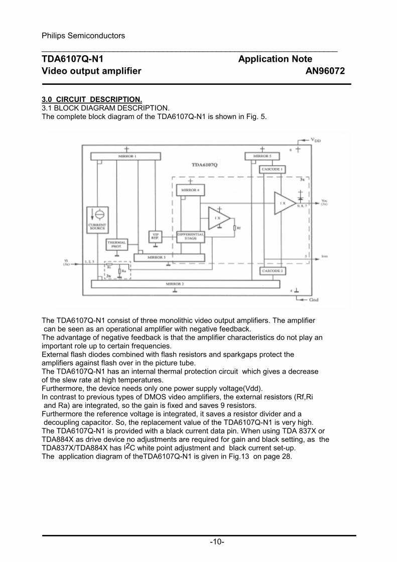
3.0 CIRCUIT DESCRIPTION.3.1 BLOCK DIAGRAM DESCRIPTION.The complete block diagram of the TDA6107Q-N1 is shown in Fig. 5.
Fig.5 Block diagram of the TDA6107Q-N1(one amplifier shown).
The TDA6107Q-N1 consist of three monolithic video output amplifiers. The amplifier can be seen as an operational amplifier with negative feedback.The advantage of negative feedback is that the amplifier characteristics do not play animportant role up to certain frequencies.External flash diodes combined with flash resistors and sparkgaps protect theamplifiers against flash over in the picture tube.The TDA6107Q-N1 has an internal thermal protection circuit which gives a decreaseof the slew rate at high temperatures.Furthermore, the device needs only one power supply voltage(Vdd).In contrast to previous types of DMOS video amplifiers, the external resistors (Rf,Ri and Ra) are integrated, so the gain is fixed and saves 9 resistors.Furthermore the reference voltage is integrated, it saves a resistor divider and a decoupling capacitor. So, the replacement value of the TDA6107Q-N1 is very high.The TDA6107Q-N1 is provided with a black current data pin. When using TDA 837X orTDA884X as drive device no adjustments are required for gain and black setting, as theTDA837X/TDA884X has I2C white point adjustment and black current set-up.The application diagram of theTDA6107Q-N1 is given in Fig.13 on page 28.
Philips Semiconductors__________________________________________________________________TDA6107Q-N1 Application NoteVideo output amplifier AN96072
-11-
3.2 FUNCTIONAL PIN DESCRIPTION.
A functional pin description is given in this chapter.
Pin 1,2,3. This is the inverting input.The input configurarion consist of a resistor Ri connectedto a virtual "ground". This virtual "ground" is the negative input of anoperational amplifier and has a DC level of 2.5 V which is directly related to the internal reference voltage of 2.5 Volts.
Pin 4. Ground.
Pin 5. This is the black current measurement output for automatic black currentstabilisation (ABS).To prevent that high video currents will flow in the TDA837X/TDA884X measuring input, the voltage on pin 5 of the TDA6107Q-N1 is limited by an internal built in zenerdiode of 7 volts.The off-set current of pin5 amounts to +/- 12 µA typ. at 3V< Vom< 6V.
Pin 6. High-voltage supply Vdd.This is the supply pin of the device. As already described, the TDA6107Q-N1 does not need a 12 V supply, this means that the current for the low voltage part is delivered by the Vdd.The pin has to be decoupled by two capacitors, one for high frequency and the other for lowfrequency decoupling. The value and the position of these capacitors is very important (seechapter 7.4 flash-over protection).
Pin 7,8,9. Cathode output.The video output current is delivered by a quasi complementary class-A/B push-pullstage, designed in DMOS technology and can source and sink a current of 20mA, forvideo output voltages of 100Vp-p with rise and fall times of 68 nSec (20%-80% ).A feature of this output stage is the low saturation voltage (typ. 10V ) and the lowvoltage drop at high level (typ.Vdd-10V).This output pin has to be connected to the cathode of the CRT via a standard resistorof 100Ω and a high-voltage flash-over protection resistor of1kΩ .A high surge clamping diode has to be applied externally, so that the cathode outputvoltage clamps at Vdd+Vdiode.
Philips Semiconductors__________________________________________________________________TDA6107Q-N1 Application NoteVideo output amplifier AN96072
-12-
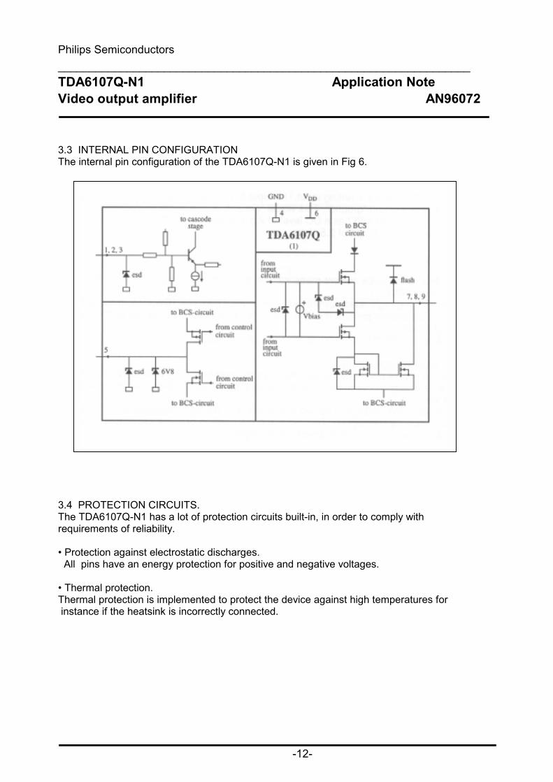
3.3 INTERNAL PIN CONFIGURATIONThe internal pin configuration of the TDA6107Q-N1 is given in Fig 6.
Fig. 6 Internal pin configurations of the TDA6107Q-N1
3.4 PROTECTION CIRCUITS.The TDA6107Q-N1 has a lot of protection circuits built-in, in order to comply withrequirements of reliability.
• Protection against electrostatic discharges. All pins have an energy protection for positive and negative voltages.
• Thermal protection.Thermal protection is implemented to protect the device against high temperatures for instance if the heatsink is incorrectly connected.
Philips Semiconductors__________________________________________________________________TDA6107Q-N1 Application NoteVideo output amplifier AN96072
-13-
4.0 DESIGN CONSIDERATIONS.
4.1 AMPLIFIER PART. The applied video output amplifier in the TDA6107Q-N1 is a negative voltage –feedback amplifier, the basic characteristics of this operational amplifier will beexplained shortly.
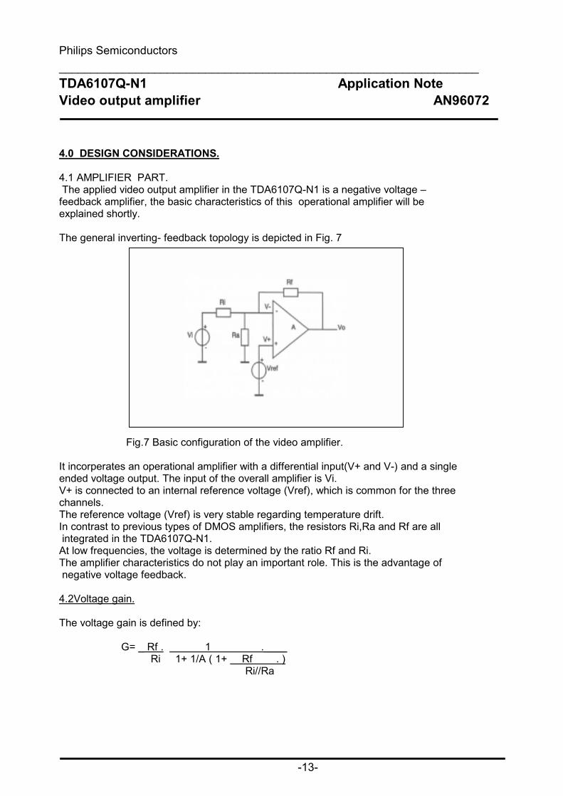
The general inverting- feedback topology is depicted in Fig. 7
Fig.7 Basic configuration of the video amplifier.
It incorperates an operational amplifier with a differential input(V+ and V-) and a singleended voltage output. The input of the overall amplifier is Vi.V+ is connected to an internal reference voltage (Vref), which is common for the threechannels.The reference voltage (Vref) is very stable regarding temperature drift.In contrast to previous types of DMOS amplifiers, the resistors Ri,Ra and Rf are all integrated in the TDA6107Q-N1.At low frequencies, the voltage is determined by the ratio Rf and Ri.The amplifier characteristics do not play an important role. This is the advantage of negative voltage feedback.
4.2Voltage gain.
The voltage gain is defined by:
G= _ Rf . 1 .____ Ri 1+ 1/A ( 1+ Rf . ) Ri//Ra

Philips Semiconductors__________________________________________________________________TDA6107Q-N1 Application NoteVideo output amplifier AN96072
-14-
Since the open loop gain A is high enough (>50 dB) ,we can approximate theequation: G = Rf/Ri
For the one-chip processor TDA837X and TDA884X family a voltage gain of 50 is sufficient to get 100Vp-p video output signals.
Rf is188.7 kΩ and Ri = 3.77 kΩ.
4.3 DC toDC transfer related to cut-off level.
The black level voltage Vo(black) is determined by Ra, Rf ,Ri and the level of Vref andVi(black). Vi(black) is the typical value of the DC black level at the input and so the typical valueof the brightness control voltage of the video processor.Vref is fixed by an internal reference voltage of the TDA6107Q-N1.
When Rf and Ri are fixed, Ra can be calculated by applying the formula:
If Vi(black) = Vref Ra = Vref . . Rf Vo(black) - Vref
The typical black level Vi(black) of the TDA837X and TDA884X is 2.5VIn this case the resistor value of Ra is independent of Ri.Ra has been chosen in such a way that the typical blacklevel output voltage Vo(black)is close to the cut-off voltage (Vco) of the picture tube.
For a cut-off level of 130V, Vref =2.5V,Ri=3.77 kΩ, Rf=188 kΩ the value of Ra=3.75kΩ.
From equation : Vo= (1+ Rf/Ra ) .Vref at Vi =Vrefthe DC to DC transfer can be plotted. This shown in Fig.1
4.4 STABILITY.The stability of the TDA6107Q-N1 is in principle quaranteed by the design. .In practice, the stability of the RGB board can be checked by :- measuring the frequency response of the system, the amplitude must be as flat as possible (within a few dB),- measuring the overshoot of a square wave signal.
For more detailed information about operational amplifier theory applied for videoamplifiers, see Appendix 1 of the application note AN95007-Application and product description of the TDA6103Q triple video output amplifier-.

Philips Semiconductors__________________________________________________________________TDA6107Q-N1 Application NoteVideo output amplifier AN96072
-15-
4.5 Black current measurement output.
The TDA6107 is provided with a black current data pin.The benefits to apply ABS are to compensate the differences in the gun characteristicsduring warming-up and ageing of the picture tube in order to have the correct colourbalance in the10µA region.The black current stabisation loop is an automatic control loop which stabilises the black current of each channel sequentially and independently.To prevent that high video currents will flow in the black current input of the contol processor, the voltage on pin 5 of the TDA6107Q-N1 is limited by an internal built inzener diode of 7V.More information about black current stabilisation with the one-chip TDA837X series isgiven in the application note AN94043 .(see references)
4.6 Flash-over protection.
The TDA6107Q-N1 needs external protection diodes (BAV21) combined with 100Ωresistors to protect the video amplifier against CRT flash-over discharges.These diodes clamp the cathode output voltage to Vdd+Vdiode. To limit the diode current, an external 1k carbon high-voltage resistor (Rfl) in series with the cathode output and a 2kV spark gap is recommended. The value of this carbon resistor is acompromise between video bandwidth and flash immunity.More details about flash protection are given in chapter 7 -"Circuit application &application hints"- and in the appendix of application note AN95064 ( see Reference).
4.7 Thermal protection.
Thermal protection is built in to protect the X-tal against high temperatures for instance ifthe heatsink is incorrectly connected.The thermal protection circuit controls the current sources and therefore also the power dissipation,resulting in 10% decrease of the slew rate at 130 oC and 30% decrease at145 oC ( typical values on the spot of the thermal protection circuit).However, this does not mean that at high temperatures around 140 oC, the performancewill be poor due to the decrease of the current Idd.Of course the h.f parameters are less, but not visible on the sreen of the CRT.

Philips Semiconductors__________________________________________________________________TDA6107Q-N1 Application NoteVideo output amplifier AN96072
-16-
5.0 EXTERNAL COMPONENTS CALCULATION.
The board described in this report is designed for the one-chip processor familyTDA837X and TDA884X.Because the gain and the DC to DC transfer are fixed by internal resistors, theimplementation of the TDA6107Q-N1 in an application is very simple and requiresonly the determination of a few external component values. These components aresupply decoupling components , which are directly related to flash protection.In addition the dissipation of the IC must be calculated in order to define the thermalresistance of the heatsink.
5.1 Decoupling [C3 and C4]
To protect the video amplifiers against picture tube flash-over discharges the high supply voltage (Vdd) must be decoupled by a capacitor >20nF/250V (e.g. a filmcapacitor of 100nF/250V with short leads and with good HF characteristics), placed asclose as possible to pins 4 and 6 of the TDA6107Q-N1 and definitely within 5mm).This capacitor limits voltage excursions of Vdd during the first part (Trise=10 nsec) of alow resistance flash.
! U = I(flash). T. = Vspark (max.) . T rise = 4 kV . 10 nsec = 1.3 V C Rfl Ch.f. 1k5 20 nF
at Ch.f. = 100nF , ! U= 0.25V.
with: V(spark(max.) = maximum ignition voltage of the sparkgap,Trise = rise time of the cathode voltage to exceed the Vspark(max.),Rfl= flash resistor,Ch.f.= high frequency decoupling capacitor.
The high supply voltage (Vdd) must also be decoupled with a capacitor ≥3.3uF/250V on the CRT board . This capacitor limits the voltage excursion during a high resistance flash. For the calculation of this voltage excursion it is supposed that there is no ignition of the spark gap and that the picture tube discharges completely through thevideo amplifier. In that case the maximal voltage excursion will be:
!U = Ctube . Veht = 1nF . 28 kV = 8.5 V Cl.f. 3.3 µF
with: Ctube = capacitance of the picture tube, the value of the capacitance is a function of the picture tube size, at a 15 inch tube Ctube is about 1nF.
Veht = voltage of extra high tension,Cl.f. = low frequency decoupling capacitor.
This means for a large size CRT , the value of Cl.f. has to be increased for the samevalue of !U.
Philips Semiconductors__________________________________________________________________TDA6107Q-N1 Application NoteVideo output amplifier AN96072
-17-
6.0 DISSIPATION & HEATSINK CALCULATION.
6.1 Static and dynamic dissipation.The dissipation of the TDA6107Q-N1 consists of the static contribution of the quiescent current and the dynamic dissipation caused by high frequency drive (proportional to frequency)
The static dissipation, incl. dissipating of the internal resistors(Rf), equals:
Pstat = Vdd. Idd + 3. [Voc. Ioc] (6-1)
Ioc = DC value of the cathode current.Voc = DC value of the cathode voltage.With Vdd=200V, Voc=100V and Iddmax=8.2 mA the static dissipationequals : Pstat= 1.64W.
The dynamic dissipation equals:Pdyn = 3. Vdd . ( Cl + Cint ) . f . Vo p-p . b. (6-2)
Cl = load capacitanceCint = internal load capacitance (4 pF)f = input frequencyVo p-p = output voltage (peak to peak)b = non blanking duty cycle.
With Vo p-p=100V(80Vpp at 4MHz), f=4MHz (sine wave), Cl=10 pF, Cint=4 pF andb=0.8, the dynamic dissipation Pdyn. equals 2.2 W.
The total dissipation Ptot=Pstat+Pdyn under given conditions is 3.84 W.
6.2 A more practical approach regarding dissipation
In the previous part , the dissipation has been calculated for the TDA6107Q-N1.However, this is a rather theoretical approach and in practice it differs from this, inparticular the dynamic dissipation. This will be explained now.In a TV set the worst case of dissipation occurs with :• a noise signal (from the tuner) in TV mode,• a multi-burst pattern (0.8-5.8MHz) in AV mode.Measurements in a TV set show a lower dynamic dissipation in TV and AV mode compared with the calculated values given in the previous part.The power dissipation respectively the junction temperature in both cases(TV and AVmode) are nearly equal under given conditions.Furthermore, it is not realistic that there will be a continuous picture containing a fullscreen of 4MHz signals .The dynamic dissipation has been measured in a TV set equipped with TDA6107Q-N1 shows a dynamic dissipation of 0.8 W at a multi- burst of 100Vpp in AV mode.The total dissipation under given practical conditions is Pstat+ Pdyn = 2.64 Watts.

Philips Semiconductors__________________________________________________________________TDA6107Q-N1 Application NoteVideo output amplifier AN96072
-18-
6.3 HEATSINK CALCULATIONBecause the TDA6107Q-N1 is provided with a thermal protection it is allowed tocalculate the heatsink with the practical total dissipation of 2.64 Watts.
Thermal resistances of the TDA6107Q-N1:Rth,j-am = 56K/W (typ).Rth,j-mb = 11 K/W (typ).
The Rth,mb-heatsink = 0.5 K/W depends on mounting method of the heatsink.The junction temperature can be calculated with equation (6-3).
Tjunction=Tamb,set + Ptot . Rth,j-amb [no heatsink] (6-3)
If the max. operating temperature in a TV set is about 65 oC, with a power dissipationof 2.64W and a thermal resistance of 56K/W, the thermal protection will be active tooearly.To realise that the thermal protection is starting at about 150oC junction temperature(120oC on the fin) , a heatsink has to be applied with a thermal resistance of:
Rth,h-a= [(Tj-Tamb)/Ptot] - [Rth,j-mb + Rth,(mb-heatsink)] ≥ 20K/W (6-4)

Philips Semiconductors__________________________________________________________________TDA6107Q-N1 Application NoteVideo output amplifier AN96072
-19-
7.0 CIRCUIT APPLICATION & APPLICATION HINTS
In this chapter information is given concerning the application of the TDA6107Q-N1 as video output stage. The circuit diagram of a complete video output stage for use in aTV-set is given in Fig. 13 on page 28. The circuit application is optimised for handlingthe output signals from the One Chip colour processor TDA837X/TDA884X in order todrive a flat square black-line CRT, with an EHT of 28kV and a cut-off voltage of 130V.The signal gain is 34 dB and the output swing is 100Vp-p.
7.1 DESIGN-IN SEQUENCE of the TDA6107Q-N1 in conjuntion with the TDA837X.
The alignment procedure is summarized below:1) Apply a signal with a black picture to the receiver.2) Set brightness and contrast to mid position.3) Set "gain" controls WPR,WPG and WPB to mid position (20hex)4) Adjust Vg2 voltage to make the black level on the R,G and B cathodes equal to the specified cut-off voltage of the CRT. This is done by looking at the highest black current measuring pulse at one of the cathodes at the beginning of the scan ( oscilloscope triggered on vertical). This pulse should be 10V below the desired cut-off voltage of the CRT.5) Apply a signal with a white picture to the TV set. Set contrast control to mid position.6) Use a colour analyzer to adjust WPR,WPG and WPB to the correct white point colour temperature.7) Check grey scale.8) Adjust the focus voltage for a sharp picture on the screen.
7.2 Printed Circuit Board.
The PCB shown in this report on page 30 is meant for evaluation purposes.The CRT base socket is JEDEC B10-277. The connecters X1(R,G,B,Iom) and X2(Supply, aqua) are pin alligned with the connecters of the one chip TDA837X demonstrationboard of PS-SLE ( Philips Semiconductors-Systems LaboratoryEindhoven, The Netherlands).
To get the optimal performance, special attention has to be payed on the following points of the PCB layout.- keep h.f. current loops as short as possible,- separate large and small signal current paths,- minimize parasitic capacitors, keep hf-signal tracks as narrow as possible,- use star point grounding, make ground and supply tracks as wide as possible.
- Concerning flash-over protection : the most important thing is that h.f. decoupling capacitor (C3=100nF) has to be placed as close as possible to pin 4 and 6 of the TDA6107Q-N1 and certainly within 5mm, the electrolytic capacitor (C4 = 3.3 µF) has to be mounted on the CRT panel.

Philips Semiconductors__________________________________________________________________TDA6107Q-N1 Application NoteVideo output amplifier AN96072
-20-
7.3 Switch-off behaviour.When a TV receiver is switched-off , several voltages become low. The cathode outputvoltage of the TDA6107Q-N1 is dependent on the input condition Vi and the highvoltage supply Vdd.The switch-off behaviour of the TDA6107Q-N1 is defined and controllable. This is due to the fact that the output pins of the TDA6107Q-N1 are still under control of the input pin for relative low supply voltages (approximately 30 V and higher).There are two types of switch-off behaviour:
7.31 Voc follows Vdd ,after switch off.Voc=f(t) is shown in fig.8This kind of switch-off is most general used.Conditions: Vi < Vref, after switch-off. (Vref=2.5V, internally).The fall time of Voc is determined by the fall time of Vdd and can be adapted by the value of the decoupling capacitor on Vdd. The minimum value (3.3µF) is limited by flash over behaviour.
7.32 Voc is switched to zero, after switch off while Vdd = high.Voc=f(t) is shown in fig.9Conditions: Vi > Vref, after switch-off.In this case the Ceht of the CRT will be discharged directly after switch off. This can be a safetyrequirement of the setmaker for service/repair.
When using TDA837X/TDA8444X, the kind of switch-off behaviour (7.3.1 or 7.3.2) canbe choosen via the I2C bus when switching from normal to standby mode.
Fig.8 Fig.9Upper: Vdd= f(t) ,50V/div, 250mS/div. Upper: Vdd= f(t) ,50V/div, 250mS/div.Lower: Voc= f(t) ,50V/div, 250mS/div. Lower: Voc= f(t) ,50V/div, 250mS/div.The 1-> and 2-> markers show the ground level. C=10µF.1-> for the upper trace and 2-> for the lower trace.
Philips Semiconductors__________________________________________________________________TDA6107Q-N1 Application NoteVideo output amplifier AN96072
-21-
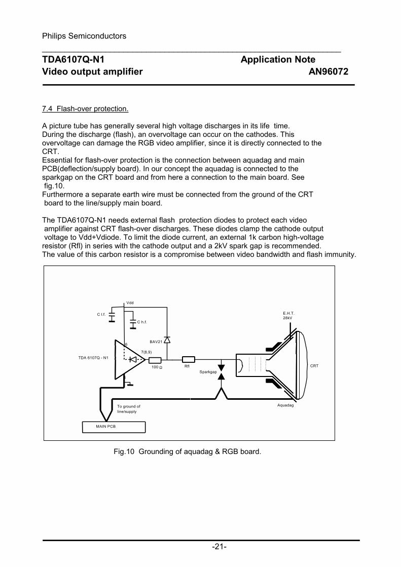
7.4 Flash-over protection.
A picture tube has generally several high voltage discharges in its life time.During the discharge (flash), an overvoltage can occur on the cathodes. Thisovervoltage can damage the RGB video amplifier, since it is directly connected to theCRT.Essential for flash-over protection is the connection between aquadag and mainPCB(deflection/supply board). In our concept the aquadag is connected to thesparkgap on the CRT board and from here a connection to the main board. See fig.10.Furthermore a separate earth wire must be connected from the ground of the CRT board to the line/supply main board.
The TDA6107Q-N1 needs external flash protection diodes to protect each video amplifier against CRT flash-over discharges. These diodes clamp the cathode output voltage to Vdd+Vdiode. To limit the diode current, an external 1k carbon high-voltageresistor (Rfl) in series with the cathode output and a 2kV spark gap is recommended.The value of this carbon resistor is a compromise between video bandwidth and flash immunity.
Fig.10 Grounding of aquadag & RGB board.
C h.f.
E.H.T.28kV
Vdd
MAIN PCB
Sparkgap
AquadagTo ground ofline/supply
4
6
CRT
C l.f.
7(8,9)
BAV21
100 RflΩ
TDA 6107Q - N1

Philips Semiconductors__________________________________________________________________TDA6107Q-N1 Application NoteVideo output amplifier AN96072
-22-
The following remarks are very important w.r.t. flash protection.
•To protect the TDA6107Q-N1 against fast voltage peaks during a low-ohmic flash pin 6 must be decoupled with a capacitor >20nF/250V with good h.f properties and placed as close as possible between pin 6 and pin 4, but definitely within 5mm.This is necessary, otherwise a voltage peak can occur due to the inductance of the long wires between the TDA6107Q-N1 pins and the capacitor (V= L di/dt) and this voltage peak can damage the IC.
• For the discharge of the CRT during a high-resistance flash an electrolitic capacitor of >3.3µF/250V is necessary, mounted on the CRT board.
• For the TDA6107Q-N1, external flash diodes and series resistors of 100Ω have to be applied at each output (see application diagram, given in Fig.13) The leads of the diodes must be kept as short as possible.
• Ignition level of the sparkgap must be typical 2kV and worst case <4kV.
• Flash resistors must be high voltage types (e.g. Allen Bradley)
• To have a short primary flash loop, earth connections of aquadag and sparkgaps arevery important.Connect the aquadag ground via a short wire ( and low inductance) to the earth of thesparkgap, and from here with a wire to the ground of the line transformer on the main PCB. The inductance can be made small, e.q. by keeping it close to the surface of thepicture tube.The ground of the TDA6107Q-N1 must be connected via a separate wire to the groundof the line transformer on the main board. The wire diagram is shown in Fig. 10 .
• Grid G1 connection. In a lot of applications, grid G1 can be directly connected to aquadag ground. In that case you can omit the flash resistor in the G1 connection to create a permanentlow impedance path for the flash current and thus better protect the cathodes , with thevideo output amplifiers.The direct aquadag grounding of G1 can't be applied when measuring the EHT info,this will be discussed in the next part.
Flash -protection for alternative aquadag grounding.
The basic application described in this report is designed for an application in which the beam current of the EHT is measured by using a "beam current " capacitor Cbc inthe line output stage.In that case, the lower side of the EHT transformer is not connected to ground (for instance the TDA837X & supply demonstration kit of PS-SLE).Therefore, special attention has to be given to flash-over behaviour.The simplfied circuit diagram is given in Fig.11.

Philips Semiconductors__________________________________________________________________TDA6107Q-N1 Application NoteVideo output amplifier AN96072
-23-
Fig.11 Alternative aqua grounding.
In case of a high resistance flash the current is low and the sparkgap does not ignite. During that flash the aquadag capacitor Ctube is discharged and the charge willtransfer via Rfl and the internal flash diode to the capacitors Cl.f. // Ch.f. and Cbc.The available charge of Ctube will be distributed across these capacitors.When Ctube=1-4 nF, Cbc=22nF and Cl.f.=3.3-10 µF the capacitor Cbc is charged at a level of several kilo Volts with a negative polarity w.r.t supply ground.At a level of 2kV the sparkgap ignites and the voltage over Cbc will be present on theoutput of the TDA6107Q-N1, resulting in a damaged IC.To prevent this, a suppression/limiter device (zenerdiode + a series diode) or VDR has to be placed from the aquadag wire (lower side of the sparkgap) on the CRT board to supply ground. This is shown in Fig.11 (limiter device).The suppression device must be a medium power type to handle the flash currents.
More detailed information about flash protection is given in the Appendix of theapplication note AN95064( see reference) .
C h.f.C l.f.
Vdd
SparkgapLimiter-device
+Vf
E.H.T.
Lineoutputtransformer
Cbc
Grounding ofaquadag &RGB-board
Groundline/supply
4
6
Beamcurrentinfo.
100 Rfl
BAV21
E.H.T.28kV
Aquadag
CRTCtube
Ω
TDA 6107Q - N1
Philips Semiconductors__________________________________________________________________TDA6107Q-N1 Application NoteVideo output amplifier AN96072
-24-
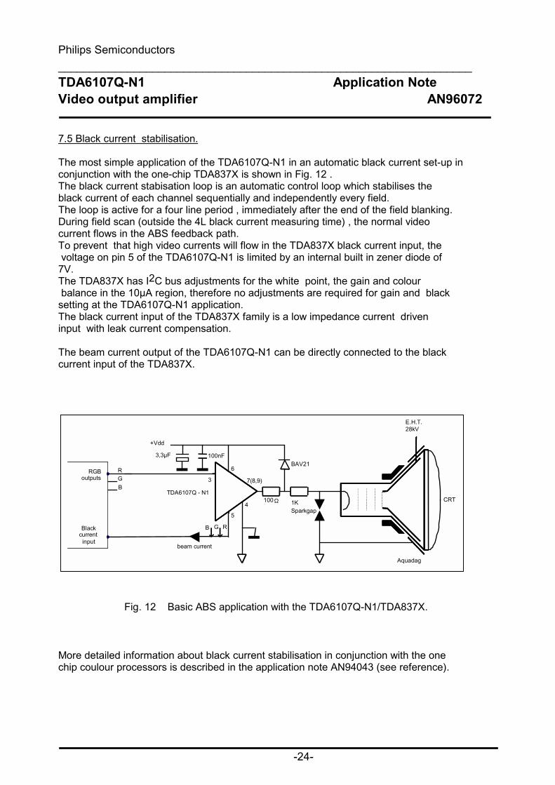
7.5 Black current stabilisation.
The most simple application of the TDA6107Q-N1 in an automatic black current set-up inconjunction with the one-chip TDA837X is shown in Fig. 12 .The black current stabisation loop is an automatic control loop which stabilises theblack current of each channel sequentially and independently every field.The loop is active for a four line period , immediately after the end of the field blanking.During field scan (outside the 4L black current measuring time) , the normal videocurrent flows in the ABS feedback path.To prevent that high video currents will flow in the TDA837X black current input, the voltage on pin 5 of the TDA6107Q-N1 is limited by an internal built in zener diode of7V.The TDA837X has I2C bus adjustments for the white point, the gain and colour balance in the 10µA region, therefore no adjustments are required for gain and blacksetting at the TDA6107Q-N1 application.The black current input of the TDA837X family is a low impedance current driveninput with leak current compensation.
The beam current output of the TDA6107Q-N1 can be directly connected to the blackcurrent input of the TDA837X.
Fig. 12 Basic ABS application with the TDA6107Q-N1/TDA837X.
More detailed information about black current stabilisation in conjunction with the onechip coulour processors is described in the application note AN94043 (see reference).
E.H.T.28kV
Aquadag
TDA6107Q - N1CRT
RGB
Blackcurrentinput
outputs6
3 7(8,9)
5
4
+Vdd
beam current
RGB
G RB
Sparkgap
BAV21
100 1KΩ
100nF3,3µF

Philips Semiconductors__________________________________________________________________TDA6107Q-N1 Application NoteVideo output amplifier AN96072
-25-
8.0 PERFORMANCE EVALUATION.
The evaluation board has been designed to obtain the best results.To evaluate the h.f performance , the best way is to measure outside the TV set bydriving the amplifier by an h.f. generator or network analyzer.The flash behaviour has to be examined in a TV set. In this situation the TDA6107Q-N1 as well as the application are tested.
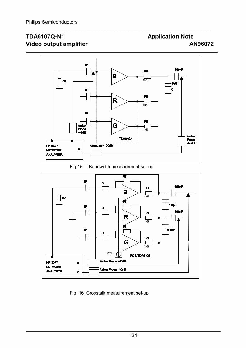
Measurement conditions for h.f. :The schematic diagram of the h.f measurement set-up is shown in Fig 15 on page 31.• High voltage supply Vdd=200V• Biasing: Voc(DC)=100V• AC Gain: 34 dB• Loading: see curves• All measurement results include a flash resistor of 1k and Cl=7pF Cl is the cathode capacitance of the CRT. The total load capacitance, including the parasitic capacitances of the PCB , will be about 10pF.
Measurement Results:
8.1 Bandwidth.
The measurement set-up is given in Fig.15 on page 31.The curves in Fig.18 and 19, on page 33, show the frequency response with 60Vp-p and100Vp-p output voltages.Rfl=1k and Cload is pF (total load capacitance about 10pF.Bandwidth at 100Vp-p, amounts to 4 MHz. (-3dB)Bandwidth at 60Vp-p, amounts to 4 MHz. (-3dB)
The value of the flash resistor is a compromise between flash-over behaviour andbandwidth.A common used value for Rfl is 1k5. For the TDA6107Q-N1 the value of Rfl is reducedto 1k, in order to compensate partly the slope of bode plot characteristic of the device.Reduction of the flash resistor is allowed due to the applied external flash protection.
8.2 Cross-talk.The measurement set-up is given in Fig.16 on page 31.A sine wave input signal is injected in one channel and the output signal of one of theother channels is measured.
Cross-talk = 20 log Voc ( drive channel) . [dB]Voc (one of the other channels)
The curves given in Fig.20, 21 and 22 on page 34 and 35 show the cross-talk of thisapplication board at which Voc= 50Vp-p .The worst value is -22 dB at 4 MHz.The cross-talk is not the same for the six different combinations of the three channels.
Philips Semiconductors__________________________________________________________________TDA6107Q-N1 Application NoteVideo output amplifier AN96072
-26-
8.2 Rise and fall time.
The curves Fig.23 and 24 on page 36 respectively show the rise and fall time at100Vp-p output signal of the red channel, measured in a TV set (AV mode).Typ. value Tf= 122 nSec. at 100Vp-p, with Rfl=1k.Typ. value Tr= 122 nSec. at 100Vp-p, with Rfl=1k.
8.4 Flash test.
Fig. 17 on page 32 shows the test set-up applied for flash-over tests by Philips.With this test, the TDA6107Q-N1 as well as the application are tested.
Test conditions:TV set with 33 inch soft flash picture tube, Veht=28 kV.So the total available charge will be Q= Ctube.Veht = 3.5nF. 28kV= 100 µC.Number of flashes: 50
8.4.1 High-resistance flash.
During high resistance flashes , the sparkgap does not ignite and the total charge transfers via the flash resistor Rm, Rfl and the flash diode into the decouplingcapacitor of Vdd.Where Rm is the simulation of the arc resistance in the CRT between g4 and thecathode.In practice , the minimum value of Rm at which the sparkgap does not ignite is :
Rm= Rfl(Veht - V(spark) = 1k(28-4)= 6kΩ V(spark) 4k
The peak current amounts to Veht / (Rm+ Rfl)= 28kV / (9k+1k)= 4 A.at which Vign of the sparkgap is worst case (4kV), Veht=28kV and Rfl=1kΩ.
At the high resistance flash-test, switch S1 is closed (Rfl=0 Ω), which means that the sparkgap can not ignite.To test at various values of flash currents, the value of Rm has to be adapted.
8.4.2 Low -resistance flash.During low-resistance flashes , S1 is open, the sparkgap ignites and only a littlecharge tranfers via the flash resistor Rfl and the flash diode into the decouplingcapacitors of Vdd.Very fast peak voltages can occur on the Vdd pin of the TDA6107Q-N1 , the h.f.capacitor has to prevent the device for these peak voltages.At a low-resistance flash , the resistor Rm (equivalent of the arc of the CRT) is typical400Ω and worst case 200Ω for a soft flash picture tube.
Philips Semiconductors__________________________________________________________________TDA6107Q-N1 Application NoteVideo output amplifier AN96072
-27-
9.0. REFERENCES.
1) DATA SHEET TDA6107Q-N1.2) DATA SHEET TDA837X3) DATA SHEET TDA884X4) Soft-flash colour tubes, PHILIPS COMPONENTS Technical publication 2535) Flashover in picture tubes and methods of protection. - By A. Ciuciura.- The Radio and Electronic Engineer, Vol.37, No3, March 1969.6) Black current stabilisation description and application for the TDA8362A,
TDA8366 and TDA8376. -AN94043- By: T. Bruton.7) Application and product description of the TDA6103Q triple video amplifier. -AN 95007- By: E.H Schutte.8) Application and product description of the TDA6106Q video output amplifier. -AN 95064- By: E.H Schutte.
APPENDIX
- Imperfections of the TDA6107Q-N1, see page 37.

Philips Semiconductors__________________________________________________________________TDA6107Q-N1 Application NoteVideo output amplifier AN96072
-28-
Fig. 13 Application diagram of the TDA6107Q-N1.

Philips Semiconductors__________________________________________________________________TDA6107Q-N1 Application NoteVideo output amplifier AN96072
-29-
PART LIST.
Position no. VALUE RATING TYPE
Integrated Circuit(s)TDA6107Q-N1
CapacitorsC1 1nF 2000V MKPC2 2n7 500V Ceramic plateC3 100nF 250V MKTC4 3.3 -10µF1) 250V Electrolytic
Resistors.
R1 1.2Ω SFR16TR2, R7 1k5 High V. Allen Bradley -1/2 WR3,R4,R5 1kΩ High V. Allen Bradley -1/2 W
R6 47Ω NFR25R8,R9,R10 100Ω SFR16T
Diodes
D1,D2,D3 BAV21Z1 24V BZD23C24Z2 BYD33M
VDR
V1(Varistor) 35V
Special parts
X1 5-pole connectorX2 6-pole connectorPicture tube socket, with integrated sparkgaps EDEC B10-277
1) At a 15 inch CRT, C4=3.3µF. 21 inch CRT, C4= 6.8µF. 29 inch CRT, C4=10µF.

Philips Semiconductors__________________________________________________________________TDA6107Q-N1 Application NoteVideo output amplifier AN96072
-30-
Scale: 1:1
Fig.14 TDA6107Q-N1 Evaluation board layout & components view.
Philips Semiconductors__________________________________________________________________TDA6107Q-N1 Application NoteVideo output amplifier AN96072
-31-
Fig.15 Bandwidth measurement set-up
Fig. 16 Crosstalk measurement set-up

Philips Semiconductors__________________________________________________________________TDA6107Q-N1 Application NoteVideo output amplifier AN96072
-32-
Fig.17 Flash-over test set-up.
Rfl = 1kΩ
The value of Rm depends on type of test (200Ω -10kΩ) and is built with resistors inseries.Type: Allen Bradley - high voltage.Rm is the simulation of the arc resitance in the picture tube between the EHT and thecathode.
Flashmill
C h.f.
E.H.T.28kV
Vdd
MAIN PCB
Sparkgap
AquadagTo ground ofline/supply
4
6
CRT
S1
Dig. scope
Currentprobe
Rm
C l.f.
8
BAV21
100 RflΩ
TDA 6107Q - N1

Philips Semiconductors__________________________________________________________________TDA6107Q-N1 Application NoteVideo output amplifier AN96072
-33-
vert. : 3dB/div.Gain[dB]
Measurementafter Rfl
Rfl=1kΩCload=10pF
Vdd=200VVoc-dc=100VVoc-ac=60V
------->f [Hz]
Fig.18 Small signal bandwidth of the TDA6107Q-N1
vert. : 3dB/div.Gain [dB
Measurementafter Rfl
Rfl=1kΩCload=10pF
Vdd=200VVoc-dc=100VVoc-ac=100V
--------> f [Hz]
Fig.19 Large signal bandwidth of the TDA6107Q-N1.

Philips Semiconductors__________________________________________________________________TDA6107Q-N1 Application NoteVideo output amplifier AN96072
-34-
vert. : 10 dB/div.Cross-talk [dB]
Measurementafter Rfl
Rfl=1kΩCload=10pF
Vdd=200VVoc-dc=100VVoc-ac=60V
------->f [Hz
Fig.20 Crosstalk behaviour of the TDA6107Q-N1 - source= R, crosstalk=B
vert. : 10 dB/div.Cross-talk [dB]
Measurementafter Rfl
Rfl=1kΩCload=10pF
Vdd=200VVoc-dc=100VVoc-ac=60V
-------> f[Hz]
Fig.21 Crosstalk behaviour of the TDA6107Q-N1 - source= G, crosstalk=B

Philips Semiconductors__________________________________________________________________TDA6107Q-N1 Application NoteVideo output amplifier AN96072
-35-
vert. : 10 dB/div.Cross-talk [dB]
Measurementafter Rfl
Rfl=1kΩCload=10pF
Vdd=200VVoc-dc=100VVoc-ac=60V
--------->f [Hz]
Fig.22 Crosstalk behaviour of the TDA6107Q-N1 - source= G, crosstalk=R
Crosstalk Blue Crosstalk Red Crosstalk GreenSignal Blue X 36dB 23dBSignal Red 34dB X 22dBSignal Green 23dB 22dB X
Table of crosstalk at a frequency of 4 Mhz.

Philips Semiconductors__________________________________________________________________TDA6107Q-N1 Application NoteVideo output amplifier AN96072
-36-
Fig.23 Fall time of the TDA6107Q-N1 at Vo= 100Vp-p
Measured with Rflash = 1k , measured in TV set.Hor: 100nS/div Vert: 20V/div
Fig.24 Rise time of the TDA6107Q-N1 at Vo= 100Vp-p
Measured with Rflash = 1k , measured in TV set.Hor: 100nS/div Vert: 20V/div

Philips Semiconductors__________________________________________________________________TDA6107Q-N1 Application NoteVideo output amplifier AN96072
-37-
APPENDIX.IMPERFECTIONS OF TDA6107Q-N1.
• Flash performance. The flash performance of the TDA6107Q-N1 is not good. For a good flash immunity with the TDA6107Q-N1 it is necessary to apply an external protection circuit (resistor & flash diode) for each channel. The N2 version will be improved regarding flash robustness, in that case it is allowed to eliminate these extra components.
• Bandwidth. The frequency characteristic is not flat. The bode plot shows a decrease of1dB, starting at 1MHz. For the TDA6107Q-N1 the value of Rfl is reduced to 1k, in order to compensate partly the slope of bode plot characteristic of the device. Reduction of the flash resistor is allowed due to the applied external flash protection.
• Rise & Fall time. The rise and fall times are too long between 10 and 90%. Between 20 and 80% it is all right.
• Brightness flickering. This effect is application/set dependent, but can be solved by the application, no extra components are needed. The N1 version is sensitive for unwanted currents in the signal ground which disturb the ABS loop. Therefore no capacitive connections between the aquadag connections on the CRT board and the signal ground, in order to prevent injection of discharge currents into the signal ground.
• ESD The maximum allowable ESD voltage for the N1 is 1000V HBM and 300V MM. However, if Vdd is decoupled properly to ground (situation when IC is mounted on the PCB board) the HBM level has been increased to over 3500V for all pins.
NOTE.All above mentioned imperfections of the N1 version will be solved at the N2 version.


![CoreI2C v5 - Digchipapplication-notes.digchip.com/056/56-39679.pdf · PWDATA[7:0] Input APB write data PRDATA[7:0] Output APB read data Interrupts INT Output Interrupt output; monitors](https://static.fdocuments.us/doc/165x107/5af40ceb7f8b9a154c8dc605/corei2c-v5-digchipapplication-notes-70-input-apb-write-data-prdata70-output.jpg)


