AN851, A FLASH Bootloader for PIC16 and PIC18...
38
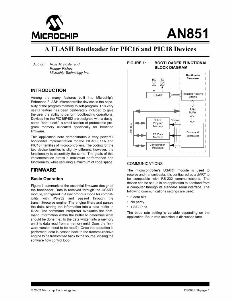
2002 Microchip Technology Inc. DS00851B-page 1 AN851 INTRODUCTION Among the many features built into Microchip’s Enhanced FLASH Microcontroller devices is the capa- bility of the program memory to self-program. This very useful feature has been deliberately included to give the user the ability to perform bootloading operations. Devices like the PIC18F452 are designed with a desig- nated “boot block”, a small section of protectable pro- gram memory allocated specifically for bootload firmware. This application note demonstrates a very powerful bootloader implementation for the PIC16F87XA and PIC18F families of microcontrollers. The coding for the two device families is slightly different; however, the functionality is essentially the same. The goals of this implementation stress a maximum performance and functionality, while requiring a minimum of code space. FIRMWARE Basic Operation Figure 1 summarizes the essential firmware design of the bootloader. Data is received through the USART module, configured in Asynchronous mode for compat- ibility with RS-232 and passed through the transmit/receive engine. The engine filters and parses the data, storing the information into a data buffer in RAM. The command interpreter evaluates the com- mand information within the buffer to determine what should be done (i.e., Is the data written into a memory unit? Is data read from a memory unit? Does the firm- ware version need to be read?). Once the operation is performed, data is passed back to the transmit/receive engine to be transmitted back to the source, closing the software flow control loop. FIGURE 1: BOOTLOADER FUNCTIONAL BLOCK DIAGRAM COMMUNICATIONS The microcontroller’s USART module is used to receive and transmit data; it is configured as a UART to be compatible with RS-232 communications. The device can be set up in an application to bootload from a computer through its standard serial interface. The following communications settings are used: • 8 data bits • No parity • 1 STOP bit The baud rate setting is variable depending on the application. Baud rate selection is discussed later. Author: Ross M. Fosler and Rodger Richey Microchip Technology Inc. USART Transmit/Receive Engine RAM Buffer Command Interpreter FLASH Program Memory EE Configuration Data Memory TX RX Registers Bootloader Control Firmware Data Bus A FLASH Bootloader for PIC16 and PIC18 Devices
Transcript of AN851, A FLASH Bootloader for PIC16 and PIC18...
AN851A FLASH Bootloader for PIC16 and PIC18 Devices
INTRODUCTIONAmong the many features built into Microchip’sEnhanced FLASH Microcontroller devices is the capa-bility of the program memory to self-program. This veryuseful feature has been deliberately included to givethe user the ability to perform bootloading operations.Devices like the PIC18F452 are designed with a desig-nated “boot block”, a small section of protectable pro-gram memory allocated specifically for bootloadfirmware.This application note demonstrates a very powerfulbootloader implementation for the PIC16F87XA andPIC18F families of microcontrollers. The coding for thetwo device families is slightly different; however, thefunctionality is essentially the same. The goals of thisimplementation stress a maximum performance andfunctionality, while requiring a minimum of code space.
FIRMWARE
Basic OperationFigure 1 summarizes the essential firmware design ofthe bootloader. Data is received through the USARTmodule, configured in Asynchronous mode for compat-ibility with RS-232 and passed through thetransmit/receive engine. The engine filters and parsesthe data, storing the information into a data buffer inRAM. The command interpreter evaluates the com-mand information within the buffer to determine whatshould be done (i.e., Is the data written into a memoryunit? Is data read from a memory unit? Does the firm-ware version need to be read?). Once the operation isperformed, data is passed back to the transmit/receiveengine to be transmitted back to the source, closing thesoftware flow control loop.
FIGURE 1: BOOTLOADER FUNCTIONAL BLOCK DIAGRAM
COMMUNICATIONS
The microcontroller’s USART module is used toreceive and transmit data; it is configured as a UART tobe compatible with RS-232 communications. Thedevice can be set up in an application to bootload froma computer through its standard serial interface. Thefollowing communications settings are used:• 8 data bits• No parity• 1 STOP bitThe baud rate setting is variable depending on theapplication. Baud rate selection is discussed later.
Author: Ross M. Fosler and Rodger RicheyMicrochip Technology Inc.
USART Transmit/ReceiveEngine
RAMBuffer
CommandInterpreter
FLASHProgramMemory
EE
Configuration
DataMemory
TXRX
Registers
Bootloader
Control
Firmware
Dat
a Bu
s
� 2002 Microchip Technology Inc. DS00851B-page 1
AN851
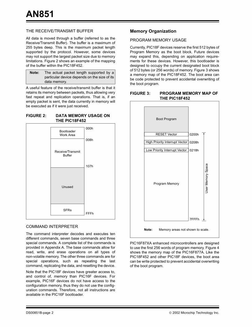
THE RECEIVE/TRANSMIT BUFFERAll data is moved through a buffer (referred to as theReceive/Transmit Buffer). The buffer is a maximum of255 bytes deep. This is the maximum packet lengthsupported by the protocol. However, some devicesmay not support the largest packet size due to memorylimitations. Figure 2 shows an example of the mappingof the buffer within the PIC18F452.
A useful feature of the receive/transmit buffer is that itretains its memory between packets, thus allowing veryfast repeat and replication operations. That is, if anempty packet is sent, the data currently in memory willbe executed as if it were just received.
FIGURE 2: DATA MEMORY USAGE ON THE PIC18F452
COMMAND INTERPRETER
The command interpreter decodes and executes tendifferent commands, seven base commands and threespecial commands. A complete list of the commands isprovided in Appendix A. The base commands allow forread, write, and erase operations on all types ofnon-volatile memory. The other three commands are forspecial operations, such as repeating the lastcommand, replicating the data, and resetting the device.Note that the PIC18F devices have greater access to,and control of, memory than PIC16F devices. Forexample, PIC16F devices do not have access to theconfiguration memory, thus they do not use the config-uration commands. Therefore, not all instructions areavailable in the PIC16F bootloader.
Memory Organization
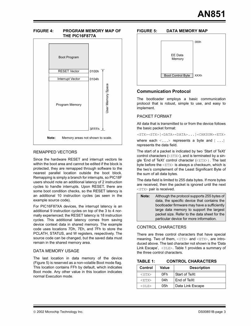
PROGRAM MEMORY USAGE
Currently, PIC18F devices reserve the first 512 bytes ofProgram Memory as the boot block. Future devicesmay expand this, depending on application require-ments for these devices. However, this bootloader isdesigned to occupy the current designated boot blockof 512 bytes (or 256 words) of memory. Figure 3 showsa memory map of the PIC18F452. The boot area canbe code protected to prevent accidental overwriting ofthe boot program.
FIGURE 3: PROGRAM MEMORY MAP OF THE PIC18F452
PIC16F87XA enhanced microcontrollers are designedto use the first 256 words of program memory. Figure 4shows the memory map of the PIC16F877A. Like thePIC18F452 and other PIC18F devices, the boot areacan be write protected to prevent accidental overwritingof the boot program.
Note: The actual packet length supported by aparticular device depends on the size of itsdata memory.
107h
Unused
008h
Receive/TransmitBuffer
FFFh
000hBootloaderWork Area
SFRs
RESET Vector
Low Priority Interrupt Vector
0200h
0218h
Program Memory
High Priority Interrupt Vector 0208h
Use
r Mem
ory
Spac
e
7FFFh
Boot Program
Note: Memory areas not shown to scale.
DS00851B-page 2 � 2002 Microchip Technology Inc.
AN851
FIGURE 4: PROGRAM MEMORY MAP OFTHE PIC16F877A
REMAPPED VECTORS
Since the hardware RESET and interrupt vectors liewithin the boot area and cannot be edited if the block isprotected, they are remapped through software to thenearest parallel location outside the boot block.Remapping is simply a branch for interrupts, so PIC18Fusers should note an additional latency of 2 instructioncycles to handle interrupts. Upon RESET, there aresome boot condition checks, so the RESET latency isan additional 10 instruction cycles (as seen in theexample source code). For PIC16F87XA devices, the interrupt latency is anadditional 9 instruction cycles on top of the 3 to 4 nor-mally experienced; the RESET latency is 18 instructioncycles. This additional latency comes from savingdevice context data in shared memory. The examplecode uses locations 7Dh, 7Eh, and 7Fh to store thePCLATH, STATUS, and W registers, respectively. Thesource code can be changed, but the saved data mustremain in the shared memory area.
DATA MEMORY USAGE
The last location in data memory of the device(Figure 5) is reserved as a non-volatile Boot mode flag.This location contains FFh by default, which indicatesBoot mode. Any other value in this location indicatesnormal Execution mode.
FIGURE 5: DATA MEMORY MAP
Communication ProtocolThe bootloader employs a basic communicationprotocol that is robust, simple to use, and easy toimplement.
PACKET FORMAT
All data that is transmitted to or from the device followsthe basic packet format:<STX><STX>[<DATA><DATA>...]<CHKSUM><ETX>
where each <...> represents a byte and [...]represents the data field. The start of a packet is indicated by two ‘Start of TeXt’control characters (<STX>), and is terminated by a sin-gle ‘End of TeXt’ control character (<ETX>). The lastbyte before the <ETX> is always a checksum, which isthe two’s complement of the Least Significant Byte ofthe sum of all data bytes. The data field is limited to 255 data bytes. If more bytesare received, then the packet is ignored until the next<STX> pair is received.
CONTROL CHARACTERS
There are three control characters that have specialmeaning. Two of them, <STX> and <ETX>, are intro-duced above. The last character not shown is the ‘DataLink Escape’, <DLE>. Table 1 provides a summary ofthe three control characters.
RESET Vector 0100h
Program Memory
Interrupt Vector 0104h
Use
r Mem
ory
Spac
e
3FFFh
Boot Program
Note: Memory areas not shown to scale.
Note: Although the protocol supports 255 bytes ofdata, the specific device that contains thebootloader firmware may have a sufficientlylarge data memory to support the largestpacket size. Refer to the data sheet for theparticular device for more information.
TABLE 1: CONTROL CHARACTERSControl Value Description
<STX> 0Fh Start of TeXt<ETX> 04h End of TeXt<DLE> 05h Data Link Escape
EE Data
Boot Control Byte XXXh
000h
Memory
� 2002 Microchip Technology Inc. DS00851B-page 3
AN851
The <DLE> is used to identify a value that could beinterpreted in the data field as a control character.Within the data field, the bootloader will always acceptthe byte following a <DLE> as data, and will alwayssend a <DLE> before any of the three control charac-ters. For example, if a byte of value 0Fh is transmittedas part of the data field, rather than as the <STX> con-trol character, the <DLE> character is inserted beforethe <STX>. This is called “byte stuffing”.COMMANDS
The data field for each packet contains one commandand its associated data. The commands are detailed inAppendix A.
COMMAND RESPONSE LATENCY
Flow control is built into the protocol. Thus, for everyreceived command (except RESET), there is aresponse. If there is no response, then one (or more) ofthe following has happened:• the data was corrupted (bad checksum)• the packet was never received• the data field was too long• RESET was executedSo how long do you wait before deciding a problem hasoccurred? The response latency (shown in Figure 6) isdependent on the amount of data sent, the commandbeing executed, and the clock frequency. For read commands, the latency is highly dependenton the clock frequency, and the size of the packet. Fora small packet at high frequency, the response isalmost immediate, typically on the order of a few micro-seconds. For large packets, the latency could be on theorder of hundreds of microseconds. In general, read commands require very little time com-pared to write commands. Write commands are mostlydependent on internally timed write cycles. For exam-ple, the typical write time required for a singleEEPROM location is 4 ms. If the maximum packet size(250 bytes of writable data) was sent, the receive totransmit latency would be about 1 second.
FIGURE 6: RECEIVE TO TRANSMIT LATENCY
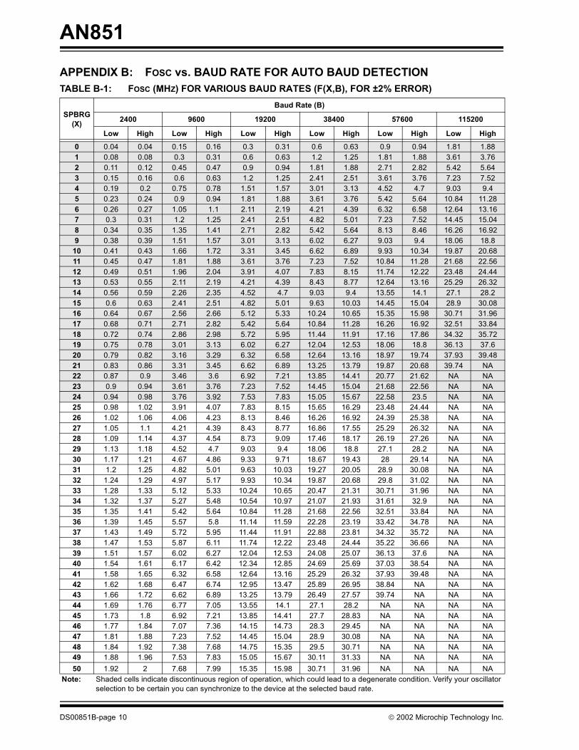
Automatic Baud Rate DetectionThe bootloader is provided with an automatic baud ratedetection algorithm that will detect most baud rates formost input clock frequencies (FOSC). The algorithmdetermines the best value for the Baud Rate Generatorand then loads the SPBRG register on themicrocontroller with the determined value.
SYNCHRONIZING
The first <STX> in the protocol is the synchronizationbyte. It is used to match the device’s baud rate to thesource’s baud rate. Thus, the device is synchronized tothe source on every new packet.
SELECTING FOSC AND BAUD RATE
The recommended baud rate for this application is9600 bps. This is the ideal rate for a device operatingfrom 4 MHz, to the device’s maximum operating fre-quency (40 MHz in most cases). Higher baud rates arepossible, but degenerate conditions can occur.There are a few clock frequency/standard baud ratecombinations that lead to a degenerate baud rateselection during synchronization; under such condi-tions, the device will never synchronize to the source.Clock frequencies that avoid such degenerateconditions are given by the equation:
where E is the error (typically 2%), X is the value for theSPBRG register, and B is the baud rate. A table of cal-culated clock oscillator ranges for most of the commonbaud rates is provided in Appendix B for quickreference.
BOOTING A DEVICE
Entering and Leaving Boot ModeWith the bootloader firmware loaded, there are two dis-tinct modes of operation: Boot Mode and User Mode.The bootloader uses the last location of data memoryto determine which mode to run in. A value of FFh indi-cates Boot mode. Any other value indicates Usermode. Thus, a new part with its data memory notinitialized will automatically enter Boot mode the firsttime.
Note: Control characters are not considered dataand are not included in the checksum.
RX
TX
Delay
Note: Refer to the specific device data sheet forinformation about the USART module andits associated registers.
Note: If a ‘Start of TeXt’ condition is receivedduring the reception of a packet, then nosynchronization occurs.
FOSC = (1 ± E)(X + 1)(16)(B)
DS00851B-page 4 � 2002 Microchip Technology Inc.
AN851
To leave Boot mode, the last location must be changedto some value other than FFh. Then, a device RESET(hardware or software) is initiated. For PIC18F devices,the RESET command actually generates a true RESETvia the RESET instruction (same as MCLR). Other thantying a port pin to MCLR, a true RESET is not possiblein firmware on PIC16F87XA devices. Although theRESET command is supported, it only causes thePIC16F device to jump to the RESET vector; the regis-ters used to perform bootload operations are notchanged to their RESET states.Reading/Writing/Erasing Program Memory
PIC18F
For the PIC18F devices, commands 1 through 3 sup-port operations to FLASH program memory. Readoperations occur at the byte level. Write operations areperformed on multiples of 8 bytes (one block). Eraseoperations are performed on 64 bytes (one row).When writing program memory on a PIC18F device,the memory should be erased. The default operation is:bits can only be cleared when written to. An erase oper-ation is the only action that can be used to set bits inprogram memory. Thus, if the bootloader protectionbits are not setup in the configuration bytes, operationson memory from 000h to 1FFh could partially, orcompletely disable the bootloader firmware.User IDs (starting at address 200000h) are consideredto be part of program memory and are written anderased like normal FLASH program memory. TheDevice ID (addresses 3FFFFEh and 3FFFFFh) is alsoconsidered program memory. While they can beaccessed, however, they are read only and cannot bealtered.
PIC16F
The PIC16F87XA devices support reading and writingto program memory. Commands 1 and 2 support oper-ations to FLASH program memory. Read operationsoccur at the word level (2 bytes). Write operations areperformed on multiples of 4 words (8 bytes). Sincewrite operations are erase-before-write, the erase com-mand is not supported. The bootloader area, from 000hto 0FFh, should be write protected to preventoverwriting itself.Neither the User ID nor the Device ID locations areaccessible during normal operation on the PIC16 archi-tecture; therefore, these areas can neither be read norwritten.
Reading/Writing Data MemoryData memory is read or written one byte at a time,through commands 4 and 5. Since it is not actuallymapped to the normal FLASH memory space, theaddress starts at 000h and continues to the end ofEEDATA memory. Note that the last location of the data memory is usedas a boot flag. Writing anything other than FFh to thelast location indicates normal code execution.
Configuration Bits
PIC18F
PIC18F devices allow access to the device configura-tion bits (addresses starting at 300000h) during normaloperation. In the bootloader, commands 6 and 7 pro-vide this access. Data is read one byte at a time and,unlike program memory, is written one byte at a time.Since configuration bits are automatically erasedbefore being written, there is no erase command forconfiguration memory.Having access to configuration settings is very power-ful; it is also potentially very dangerous. For example,assume that the system is designed to run in HS mode,with a 20 MHz crystal. If the bootloader changes theoscillator setting to LP mode, the system will cease tofunction — including the bootloader! Basically, thesystem has been killed by improperly changing one bit.It is also important to note some configuration bits aresingle direction bits in Normal mode; they can only bechanged to one state, and cannot be changed back.The code protection bits in Configuration Registers 5Land 5H are a good example. If any type of code protec-tion is enabled for a block, it cannot be disabled withouta device programmer. Essentially, the bootloadercannot reverse code protection.
PIC16F
The configuration memory is not accessible during nor-mal operation on the PIC16 architecture; therefore, thisarea can neither be read nor written.
� 2002 Microchip Technology Inc. DS00851B-page 5
AN851
WRITING CODEThe bootloader operates as a separate entity, whichmeans that an application can be developed with verylittle concern about what the bootloader is doing. Thisis as it should be; the bootloader should be dormantcode until an event initiates a boot operation. Underideal circumstances, bootloader code should never berunning during an application’s intended normaloperation.When developing an application with a residentbootloader, some basic principles must be kept inmind:Writing in AssemblyWhen writing in assembly, the boot block and new vec-tors must be considered. For modular code, this is gen-erally just a matter of changing the linker script file forthe project. An example is given in Appendix D. If anabsolute address is assigned to a code section, theaddress must point somewhere above the boot block.For those who write absolute assembly, all that is nec-essary is to remember that for PIC18F devices, thenew RESET vector is at 200h, and the interrupt vectorsare at 208h and 218h. For PIC16F87XA devices, theRESET vector is at 100h and the interrupt vector is at104h. No code, except the bootloader, should reside inthe boot block.
Writing in CWhen using the MPLAB® C18 C compiler to developPIC18F firmware for an application, the standardstart-up object (c018.o or c018i.o) must be rebuiltwith the new RESET vector. Like modular assembly,the linker file must be changed to incorporate the pro-tected boot block and new vectors. Appendix D showsan example linker file.For users of other compilers, for either PIC16F87XA orPIC18F devices, check with the compiler’s softwareuser guide to determine how to change the start-upcode and vectors.
Bootloader Re-EntryIf the need exists to re-enter Boot mode from the appli-cation (and it usually does), the last location of the datamemory must be set to FFh. The code in Example 1demonstrates how this might be done in an applicationon a PIC18F device. Since the bootloader assumesRESET conditions, a RESET instruction should beinitiated after setting the last location.
EXAMPLE 1: SETTING THE LAST LOCATION OF THE DATA MEMORY
DebuggingFor most situations, it is not necessary to have thebootloader firmware in memory to do debugging of anapplication with either the MPLAB ICD 2 or ICEdevices. However, branch statements must be insertedat the hardware vectors to get to the new designatedvectors. It may also be useful to have the start-up tim-ing match exactly to the bootloader entry. When devel-opment of the application is finished, either remove thebranches and rebuild the project, or export only thememory above the boot block. This code can then bedistributed to those who are updating their firmware.
setf EEADR ; Point to the last bytesetf EEADRHsetf EEDATA ; Bootmode control bytemovlw b'00000100 ; Setup for EEDatamovwf EECON1movlw 0x55 ; Unlockmovwf EECON2movlw 0xAAmovwf EECON2bsf EECON1, WR ; Start the writenopbtfsc EECON1, WR ; Waitbra $ - 2reset
DS00851B-page 6 � 2002 Microchip Technology Inc.
AN851
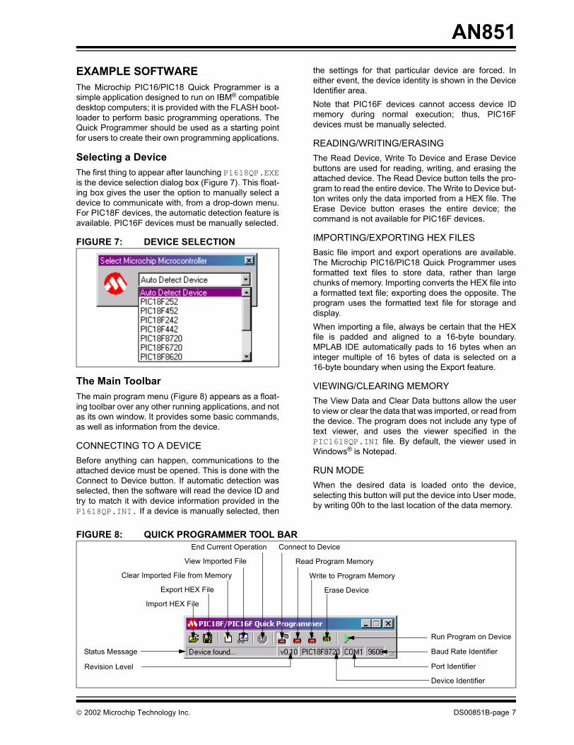
EXAMPLE SOFTWAREThe Microchip PIC16/PIC18 Quick Programmer is asimple application designed to run on IBM® compatibledesktop computers; it is provided with the FLASH boot-loader to perform basic programming operations. TheQuick Programmer should be used as a starting pointfor users to create their own programming applications.Selecting a DeviceThe first thing to appear after launching P1618QP.EXEis the device selection dialog box (Figure 7). This float-ing box gives the user the option to manually select adevice to communicate with, from a drop-down menu.For PIC18F devices, the automatic detection feature isavailable. PIC16F devices must be manually selected.
FIGURE 7: DEVICE SELECTION
The Main ToolbarThe main program menu (Figure 8) appears as a float-ing toolbar over any other running applications, and notas its own window. It provides some basic commands,as well as information from the device.
CONNECTING TO A DEVICEBefore anything can happen, communications to theattached device must be opened. This is done with theConnect to Device button. If automatic detection wasselected, then the software will read the device ID andtry to match it with device information provided in theP1618QP.INI. If a device is manually selected, then
the settings for that particular device are forced. Ineither event, the device identity is shown in the DeviceIdentifier area.Note that PIC16F devices cannot access device IDmemory during normal execution; thus, PIC16Fdevices must be manually selected.
READING/WRITING/ERASING The Read Device, Write To Device and Erase Devicebuttons are used for reading, writing, and erasing theattached device. The Read Device button tells the pro-gram to read the entire device. The Write to Device but-ton writes only the data imported from a HEX file. TheErase Device button erases the entire device; thecommand is not available for PIC16F devices.
IMPORTING/EXPORTING HEX FILESBasic file import and export operations are available.The Microchip PIC16/PIC18 Quick Programmer usesformatted text files to store data, rather than largechunks of memory. Importing converts the HEX file intoa formatted text file; exporting does the opposite. Theprogram uses the formatted text file for storage anddisplay.When importing a file, always be certain that the HEXfile is padded and aligned to a 16-byte boundary.MPLAB IDE automatically pads to 16 bytes when aninteger multiple of 16 bytes of data is selected on a16-byte boundary when using the Export feature.
VIEWING/CLEARING MEMORYThe View Data and Clear Data buttons allow the userto view or clear the data that was imported, or read fromthe device. The program does not include any type oftext viewer, and uses the viewer specified in thePIC1618QP.INI file. By default, the viewer used inWindows® is Notepad.
RUN MODEWhen the desired data is loaded onto the device,selecting this button will put the device into User mode,by writing 00h to the last location of the data memory.
FIGURE 8: QUICK PROGRAMMER TOOL BAR
Import HEX File
Export HEX File
View Imported File
Clear Imported File from Memory
End Current Operation
Erase Device
Read Program Memory
Write to Program Memory
Connect to Device
Run Program on Device
Baud Rate Identifier
Port Identifier
Status Message
Device Identifier
Revision Level
� 2002 Microchip Technology Inc. DS00851B-page 7
AN851
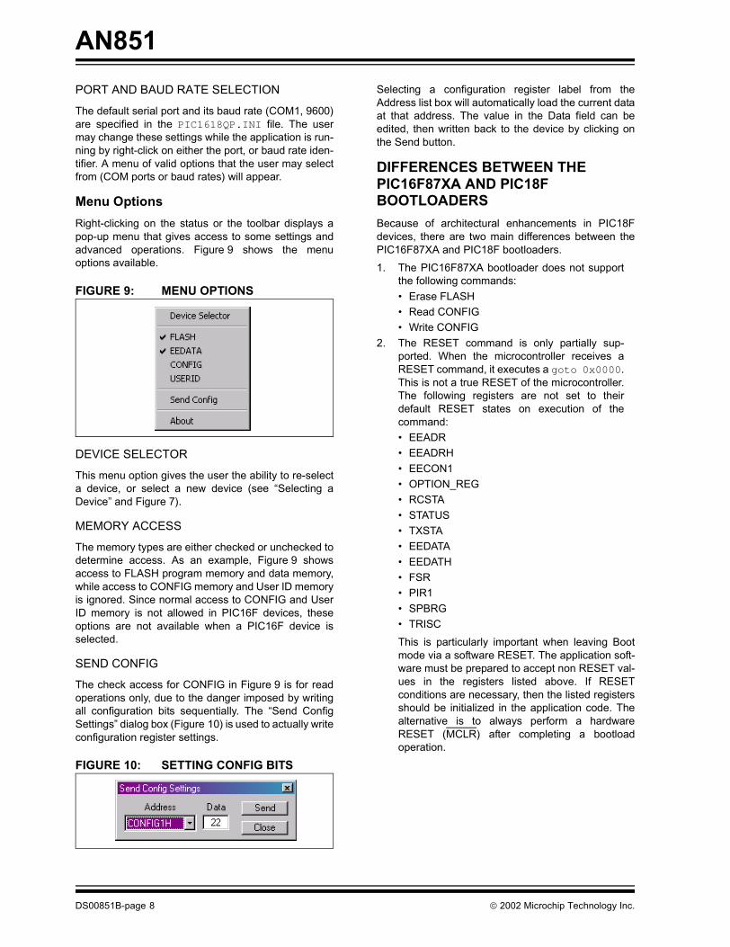
PORT AND BAUD RATE SELECTIONThe default serial port and its baud rate (COM1, 9600)are specified in the PIC1618QP.INI file. The usermay change these settings while the application is run-ning by right-click on either the port, or baud rate iden-tifier. A menu of valid options that the user may selectfrom (COM ports or baud rates) will appear.
Menu OptionsRight-clicking on the status or the toolbar displays apop-up menu that gives access to some settings andadvanced operations. Figure 9 shows the menuoptions available.
FIGURE 9: MENU OPTIONS
DEVICE SELECTOR
This menu option gives the user the ability to re-selecta device, or select a new device (see “Selecting aDevice” and Figure 7).
MEMORY ACCESS
The memory types are either checked or unchecked todetermine access. As an example, Figure 9 showsaccess to FLASH program memory and data memory,while access to CONFIG memory and User ID memoryis ignored. Since normal access to CONFIG and UserID memory is not allowed in PIC16F devices, theseoptions are not available when a PIC16F device isselected.
SEND CONFIG
The check access for CONFIG in Figure 9 is for readoperations only, due to the danger imposed by writingall configuration bits sequentially. The “Send ConfigSettings” dialog box (Figure 10) is used to actually writeconfiguration register settings.
FIGURE 10: SETTING CONFIG BITS
Selecting a configuration register label from theAddress list box will automatically load the current dataat that address. The value in the Data field can beedited, then written back to the device by clicking onthe Send button.
DIFFERENCES BETWEEN THE PIC16F87XA AND PIC18F BOOTLOADERSBecause of architectural enhancements in PIC18Fdevices, there are two main differences between thePIC16F87XA and PIC18F bootloaders.1. The PIC16F87XA bootloader does not support
the following commands:• Erase FLASH• Read CONFIG• Write CONFIG
2. The RESET command is only partially sup-ported. When the microcontroller receives aRESET command, it executes a goto 0x0000.This is not a true RESET of the microcontroller.The following registers are not set to theirdefault RESET states on execution of thecommand:• EEADR• EEADRH• EECON1• OPTION_REG• RCSTA• STATUS• TXSTA• EEDATA• EEDATH• FSR• PIR1• SPBRG• TRISCThis is particularly important when leaving Bootmode via a software RESET. The application soft-ware must be prepared to accept non RESET val-ues in the registers listed above. If RESETconditions are necessary, then the listed registersshould be initialized in the application code. Thealternative is to always perform a hardwareRESET (MCLR) after completing a bootloadoperation.
DS00851B-page 8 � 2002 Microchip Technology Inc.
AN851
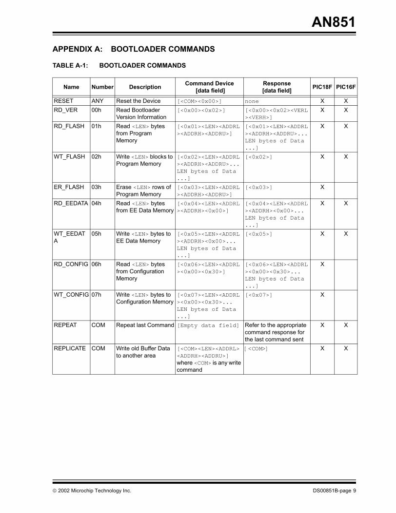
APPENDIX A: BOOTLOADER COMMANDSTABLE A-1: BOOTLOADER COMMANDS
Name Number Description Command Device [data field]
Response [data field] PIC18F PIC16F
RESET ANY Reset the Device [<COM><0x00>] none X XRD_VER 00h Read Bootloader
Version Information[<0x00><0x02>] [<0x00><0x02><VERL
><VERH>]X X
RD_FLASH 01h Read <LEN> bytes from Program Memory
[<0x01><LEN><ADDRL><ADDRH><ADDRU>]
[<0x01><LEN><ADDRL><ADDRH><ADDRU>...LEN bytes of Data ...]
X X
WT_FLASH 02h Write <LEN> blocks to Program Memory
[<0x02><LEN><ADDRL><ADDRH><ADDRU>...LEN bytes of Data ...]
[<0x02>] X X
ER_FLASH 03h Erase <LEN> rows of Program Memory
[<0x03><LEN><ADDRL><ADDRH><ADDRU>]
[<0x03>] X
RD_EEDATA 04h Read <LEN> bytes from EE Data Memory
[<0x04><LEN><ADDRL><ADDRH><0x00>]
[<0x04><LEN><ADDRL><ADDRH><0x00>...LEN bytes of Data...]
X X
WT_EEDATA
05h Write <LEN> bytes to EE Data Memory
[<0x05><LEN><ADDRL><ADDRH><0x00>...LEN bytes of Data ...]
[<0x05>] X X
RD_CONFIG 06h Read <LEN> bytes from Configuration Memory
[<0x06><LEN><ADDRL><0x00><0x30>]
[<0x06><LEN><ADDRL><0x00><0x30>...LEN bytes of Data ...]
X
WT_CONFIG 07h Write <LEN> bytes to Configuration Memory
[<0x07><LEN><ADDRL><0x00><0x30>...LEN bytes of Data...]
[<0x07>] X
REPEAT COM Repeat last Command [Empty data field] Refer to the appropriate command response for the last command sent
X X
REPLICATE COM Write old Buffer Data to another area
[<COM><LEN><ADDRL><ADDRH><ADDRU>]where <COM> is any write command
[<COM>] X X
� 2002 Microchip Technology Inc. DS00851B-page 9
AN851
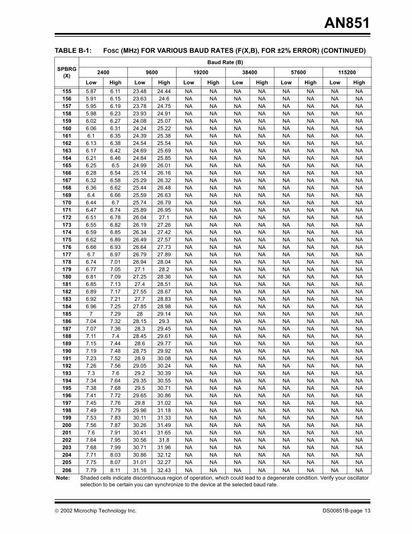
APPENDIX B: FOSC vs. BAUD RATE FOR AUTO BAUD DETECTIONTABLE B-1: FOSC (MHZ) FOR VARIOUS BAUD RATES (F(X,B), FOR ±2% ERROR)SPBRG(X)
Baud Rate (B)
2400 9600 19200 38400 57600 115200
Low High Low High Low High Low High Low High Low High0 0.04 0.04 0.15 0.16 0.3 0.31 0.6 0.63 0.9 0.94 1.81 1.881 0.08 0.08 0.3 0.31 0.6 0.63 1.2 1.25 1.81 1.88 3.61 3.762 0.11 0.12 0.45 0.47 0.9 0.94 1.81 1.88 2.71 2.82 5.42 5.643 0.15 0.16 0.6 0.63 1.2 1.25 2.41 2.51 3.61 3.76 7.23 7.524 0.19 0.2 0.75 0.78 1.51 1.57 3.01 3.13 4.52 4.7 9.03 9.45 0.23 0.24 0.9 0.94 1.81 1.88 3.61 3.76 5.42 5.64 10.84 11.286 0.26 0.27 1.05 1.1 2.11 2.19 4.21 4.39 6.32 6.58 12.64 13.167 0.3 0.31 1.2 1.25 2.41 2.51 4.82 5.01 7.23 7.52 14.45 15.048 0.34 0.35 1.35 1.41 2.71 2.82 5.42 5.64 8.13 8.46 16.26 16.929 0.38 0.39 1.51 1.57 3.01 3.13 6.02 6.27 9.03 9.4 18.06 18.8
10 0.41 0.43 1.66 1.72 3.31 3.45 6.62 6.89 9.93 10.34 19.87 20.6811 0.45 0.47 1.81 1.88 3.61 3.76 7.23 7.52 10.84 11.28 21.68 22.5612 0.49 0.51 1.96 2.04 3.91 4.07 7.83 8.15 11.74 12.22 23.48 24.4413 0.53 0.55 2.11 2.19 4.21 4.39 8.43 8.77 12.64 13.16 25.29 26.3214 0.56 0.59 2.26 2.35 4.52 4.7 9.03 9.4 13.55 14.1 27.1 28.215 0.6 0.63 2.41 2.51 4.82 5.01 9.63 10.03 14.45 15.04 28.9 30.0816 0.64 0.67 2.56 2.66 5.12 5.33 10.24 10.65 15.35 15.98 30.71 31.9617 0.68 0.71 2.71 2.82 5.42 5.64 10.84 11.28 16.26 16.92 32.51 33.8418 0.72 0.74 2.86 2.98 5.72 5.95 11.44 11.91 17.16 17.86 34.32 35.7219 0.75 0.78 3.01 3.13 6.02 6.27 12.04 12.53 18.06 18.8 36.13 37.620 0.79 0.82 3.16 3.29 6.32 6.58 12.64 13.16 18.97 19.74 37.93 39.4821 0.83 0.86 3.31 3.45 6.62 6.89 13.25 13.79 19.87 20.68 39.74 NA22 0.87 0.9 3.46 3.6 6.92 7.21 13.85 14.41 20.77 21.62 NA NA23 0.9 0.94 3.61 3.76 7.23 7.52 14.45 15.04 21.68 22.56 NA NA24 0.94 0.98 3.76 3.92 7.53 7.83 15.05 15.67 22.58 23.5 NA NA25 0.98 1.02 3.91 4.07 7.83 8.15 15.65 16.29 23.48 24.44 NA NA26 1.02 1.06 4.06 4.23 8.13 8.46 16.26 16.92 24.39 25.38 NA NA27 1.05 1.1 4.21 4.39 8.43 8.77 16.86 17.55 25.29 26.32 NA NA28 1.09 1.14 4.37 4.54 8.73 9.09 17.46 18.17 26.19 27.26 NA NA29 1.13 1.18 4.52 4.7 9.03 9.4 18.06 18.8 27.1 28.2 NA NA30 1.17 1.21 4.67 4.86 9.33 9.71 18.67 19.43 28 29.14 NA NA31 1.2 1.25 4.82 5.01 9.63 10.03 19.27 20.05 28.9 30.08 NA NA32 1.24 1.29 4.97 5.17 9.93 10.34 19.87 20.68 29.8 31.02 NA NA33 1.28 1.33 5.12 5.33 10.24 10.65 20.47 21.31 30.71 31.96 NA NA34 1.32 1.37 5.27 5.48 10.54 10.97 21.07 21.93 31.61 32.9 NA NA35 1.35 1.41 5.42 5.64 10.84 11.28 21.68 22.56 32.51 33.84 NA NA36 1.39 1.45 5.57 5.8 11.14 11.59 22.28 23.19 33.42 34.78 NA NA37 1.43 1.49 5.72 5.95 11.44 11.91 22.88 23.81 34.32 35.72 NA NA38 1.47 1.53 5.87 6.11 11.74 12.22 23.48 24.44 35.22 36.66 NA NA39 1.51 1.57 6.02 6.27 12.04 12.53 24.08 25.07 36.13 37.6 NA NA40 1.54 1.61 6.17 6.42 12.34 12.85 24.69 25.69 37.03 38.54 NA NA41 1.58 1.65 6.32 6.58 12.64 13.16 25.29 26.32 37.93 39.48 NA NA42 1.62 1.68 6.47 6.74 12.95 13.47 25.89 26.95 38.84 NA NA NA43 1.66 1.72 6.62 6.89 13.25 13.79 26.49 27.57 39.74 NA NA NA44 1.69 1.76 6.77 7.05 13.55 14.1 27.1 28.2 NA NA NA NA45 1.73 1.8 6.92 7.21 13.85 14.41 27.7 28.83 NA NA NA NA46 1.77 1.84 7.07 7.36 14.15 14.73 28.3 29.45 NA NA NA NA47 1.81 1.88 7.23 7.52 14.45 15.04 28.9 30.08 NA NA NA NA48 1.84 1.92 7.38 7.68 14.75 15.35 29.5 30.71 NA NA NA NA49 1.88 1.96 7.53 7.83 15.05 15.67 30.11 31.33 NA NA NA NA50 1.92 2 7.68 7.99 15.35 15.98 30.71 31.96 NA NA NA NA
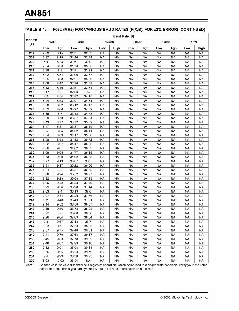
Note: Shaded cells indicate discontinuous region of operation, which could lead to a degenerate condition. Verify your oscillator selection to be certain you can synchronize to the device at the selected baud rate.
DS00851B-page 10 � 2002 Microchip Technology Inc.
AN851
51 1.96 2.04 7.83 8.15 15.65 16.29 31.31 32.59 NA NA NA NA52 1.99 2.08 7.98 8.3 15.96 16.61 31.91 33.21 NA NA NA NA53 2.03 2.12 8.13 8.46 16.26 16.92 32.51 33.84 NA NA NA NA54 2.07 2.15 8.28 8.62 16.56 17.23 33.12 34.47 NA NA NA NA55 2.11 2.19 8.43 8.77 16.86 17.55 33.72 35.09 NA NA NA NA56 2.15 2.23 8.58 8.93 17.16 17.86 34.32 35.72 NA NA NA NA57 2.18 2.27 8.73 9.09 17.46 18.17 34.92 36.35 NA NA NA NA58 2.22 2.31 8.88 9.24 17.76 18.49 35.52 36.97 NA NA NA NA59 2.26 2.35 9.03 9.4 18.06 18.8 36.13 37.6 NA NA NA NA60 2.3 2.39 9.18 9.56 18.36 19.11 36.73 38.23 NA NA NA NA61 2.33 2.43 9.33 9.71 18.67 19.43 37.33 38.85 NA NA NA NA62 2.37 2.47 9.48 9.87 18.97 19.74 37.93 39.48 NA NA NA NA63 2.41 2.51 9.63 10.03 19.27 20.05 38.54 NA NA NA NA NA64 2.45 2.55 9.78 10.18 19.57 20.37 39.14 NA NA NA NA NA65 2.48 2.59 9.93 10.34 19.87 20.68 39.74 NA NA NA NA NA66 2.52 2.62 10.09 10.5 20.17 20.99 NA NA NA NA NA NA67 2.56 2.66 10.24 10.65 20.47 21.31 NA NA NA NA NA NA68 2.6 2.7 10.39 10.81 20.77 21.62 NA NA NA NA NA NA69 2.63 2.74 10.54 10.97 21.07 21.93 NA NA NA NA NA NA70 2.67 2.78 10.69 11.12 21.37 22.25 NA NA NA NA NA NA71 2.71 2.82 10.84 11.28 21.68 22.56 NA NA NA NA NA NA72 2.75 2.86 10.99 11.44 21.98 22.87 NA NA NA NA NA NA73 2.78 2.9 11.14 11.59 22.28 23.19 NA NA NA NA NA NA74 2.82 2.94 11.29 11.75 22.58 23.5 NA NA NA NA NA NA75 2.86 2.98 11.44 11.91 22.88 23.81 NA NA NA NA NA NA76 2.9 3.02 11.59 12.06 23.18 24.13 NA NA NA NA NA NA77 2.94 3.06 11.74 12.22 23.48 24.44 NA NA NA NA NA NA78 2.97 3.09 11.89 12.38 23.78 24.75 NA NA NA NA NA NA79 3.01 3.13 12.04 12.53 24.08 25.07 NA NA NA NA NA NA80 3.05 3.17 12.19 12.69 24.39 25.38 NA NA NA NA NA NA81 3.09 3.21 12.34 12.85 24.69 25.69 NA NA NA NA NA NA82 3.12 3.25 12.49 13 24.99 26.01 NA NA NA NA NA NA83 3.16 3.29 12.64 13.16 25.29 26.32 NA NA NA NA NA NA84 3.2 3.33 12.79 13.32 25.59 26.63 NA NA NA NA NA NA85 3.24 3.37 12.95 13.47 25.89 26.95 NA NA NA NA NA NA86 3.27 3.41 13.1 13.63 26.19 27.26 NA NA NA NA NA NA87 3.31 3.45 13.25 13.79 26.49 27.57 NA NA NA NA NA NA88 3.35 3.49 13.4 13.94 26.79 27.89 NA NA NA NA NA NA89 3.39 3.53 13.55 14.1 27.1 28.2 NA NA NA NA NA NA90 3.42 3.56 13.7 14.26 27.4 28.51 NA NA NA NA NA NA91 3.46 3.6 13.85 14.41 27.7 28.83 NA NA NA NA NA NA92 3.5 3.64 14 14.57 28 29.14 NA NA NA NA NA NA93 3.54 3.68 14.15 14.73 28.3 29.45 NA NA NA NA NA NA94 3.58 3.72 14.3 14.88 28.6 29.77 NA NA NA NA NA NA95 3.61 3.76 14.45 15.04 28.9 30.08 NA NA NA NA NA NA96 3.65 3.8 14.6 15.2 29.2 30.39 NA NA NA NA NA NA97 3.69 3.84 14.75 15.35 29.5 30.71 NA NA NA NA NA NA98 3.73 3.88 14.9 15.51 29.8 31.02 NA NA NA NA NA NA99 3.76 3.92 15.05 15.67 30.11 31.33 NA NA NA NA NA NA100 3.8 3.96 15.2 15.82 30.41 31.65 NA NA NA NA NA NA101 3.84 4 15.35 15.98 30.71 31.96 NA NA NA NA NA NA102 3.88 4.03 15.5 16.14 31.01 32.27 NA NA NA NA NA NA
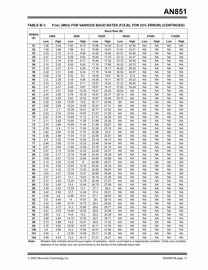
TABLE B-1: FOSC (MHZ) FOR VARIOUS BAUD RATES (F(X,B), FOR ±2% ERROR) (CONTINUED)
SPBRG(X)
Baud Rate (B)
2400 9600 19200 38400 57600 115200
Low High Low High Low High Low High Low High Low High
Note: Shaded cells indicate discontinuous region of operation, which could lead to a degenerate condition. Verify your oscillator selection to be certain you can synchronize to the device at the selected baud rate.
� 2002 Microchip Technology Inc. DS00851B-page 11
AN851
103 3.91 4.07 15.65 16.29 31.31 32.59 NA NA NA NA NA NA104 3.95 4.11 15.81 16.45 31.61 32.9 NA NA NA NA NA NA105 3.99 4.15 15.96 16.61 31.91 33.21 NA NA NA NA NA NA106 4.03 4.19 16.11 16.76 32.21 33.53 NA NA NA NA NA NA107 4.06 4.23 16.26 16.92 32.51 33.84 NA NA NA NA NA NA108 4.1 4.27 16.41 17.08 32.82 34.15 NA NA NA NA NA NA109 4.14 4.31 16.56 17.23 33.12 34.47 NA NA NA NA NA NA110 4.18 4.35 16.71 17.39 33.42 34.78 NA NA NA NA NA NA111 4.21 4.39 16.86 17.55 33.72 35.09 NA NA NA NA NA NA112 4.25 4.43 17.01 17.7 34.02 35.41 NA NA NA NA NA NA113 4.29 4.47 17.16 17.86 34.32 35.72 NA NA NA NA NA NA114 4.33 4.5 17.31 18.02 34.62 36.03 NA NA NA NA NA NA115 4.37 4.54 17.46 18.17 34.92 36.35 NA NA NA NA NA NA116 4.4 4.58 17.61 18.33 35.22 36.66 NA NA NA NA NA NA117 4.44 4.62 17.76 18.49 35.52 36.97 NA NA NA NA NA NA118 4.48 4.66 17.91 18.64 35.83 37.29 NA NA NA NA NA NA119 4.52 4.7 18.06 18.8 36.13 37.6 NA NA NA NA NA NA120 4.55 4.74 18.21 18.96 36.43 37.91 NA NA NA NA NA NA121 4.59 4.78 18.36 19.11 36.73 38.23 NA NA NA NA NA NA122 4.63 4.82 18.51 19.27 37.03 38.54 NA NA NA NA NA NA123 4.67 4.86 18.67 19.43 37.33 38.85 NA NA NA NA NA NA124 4.7 4.9 18.82 19.58 37.63 39.17 NA NA NA NA NA NA125 4.74 4.94 18.97 19.74 37.93 39.48 NA NA NA NA NA NA126 4.78 4.97 19.12 19.9 38.23 39.79 NA NA NA NA NA NA127 4.82 5.01 19.27 20.05 38.54 NA NA NA NA NA NA NA128 4.85 5.05 19.42 20.21 38.84 NA NA NA NA NA NA NA129 4.89 5.09 19.57 20.37 39.14 NA NA NA NA NA NA NA130 4.93 5.13 19.72 20.52 39.44 NA NA NA NA NA NA NA131 4.97 5.17 19.87 20.68 39.74 NA NA NA NA NA NA NA132 5.01 5.21 20.02 20.84 NA NA NA NA NA NA NA NA133 5.04 5.25 20.17 20.99 NA NA NA NA NA NA NA NA134 5.08 5.29 20.32 21.15 NA NA NA NA NA NA NA NA135 5.12 5.33 20.47 21.31 NA NA NA NA NA NA NA NA136 5.16 5.37 20.62 21.46 NA NA NA NA NA NA NA NA137 5.19 5.41 20.77 21.62 NA NA NA NA NA NA NA NA138 5.23 5.44 20.92 21.78 NA NA NA NA NA NA NA NA139 5.27 5.48 21.07 21.93 NA NA NA NA NA NA NA NA140 5.31 5.52 21.22 22.09 NA NA NA NA NA NA NA NA141 5.34 5.56 21.37 22.25 NA NA NA NA NA NA NA NA142 5.38 5.6 21.53 22.4 NA NA NA NA NA NA NA NA143 5.42 5.64 21.68 22.56 NA NA NA NA NA NA NA NA144 5.46 5.68 21.83 22.72 NA NA NA NA NA NA NA NA145 5.49 5.72 21.98 22.87 NA NA NA NA NA NA NA NA146 5.53 5.76 22.13 23.03 NA NA NA NA NA NA NA NA147 5.57 5.8 22.28 23.19 NA NA NA NA NA NA NA NA148 5.61 5.84 22.43 23.34 NA NA NA NA NA NA NA NA149 5.64 5.88 22.58 23.5 NA NA NA NA NA NA NA NA150 5.68 5.91 22.73 23.66 NA NA NA NA NA NA NA NA151 5.72 5.95 22.88 23.81 NA NA NA NA NA NA NA NA152 5.76 5.99 23.03 23.97 NA NA NA NA NA NA NA NA153 5.8 6.03 23.18 24.13 NA NA NA NA NA NA NA NA154 5.83 6.07 23.33 24.28 NA NA NA NA NA NA NA NA
TABLE B-1: FOSC (MHZ) FOR VARIOUS BAUD RATES (F(X,B), FOR ±2% ERROR) (CONTINUED)
SPBRG(X)
Baud Rate (B)
2400 9600 19200 38400 57600 115200
Low High Low High Low High Low High Low High Low High
Note: Shaded cells indicate discontinuous region of operation, which could lead to a degenerate condition. Verify your oscillator selection to be certain you can synchronize to the device at the selected baud rate.
DS00851B-page 12 � 2002 Microchip Technology Inc.
AN851
155 5.87 6.11 23.48 24.44 NA NA NA NA NA NA NA NA156 5.91 6.15 23.63 24.6 NA NA NA NA NA NA NA NA157 5.95 6.19 23.78 24.75 NA NA NA NA NA NA NA NA158 5.98 6.23 23.93 24.91 NA NA NA NA NA NA NA NA159 6.02 6.27 24.08 25.07 NA NA NA NA NA NA NA NA160 6.06 6.31 24.24 25.22 NA NA NA NA NA NA NA NA161 6.1 6.35 24.39 25.38 NA NA NA NA NA NA NA NA162 6.13 6.38 24.54 25.54 NA NA NA NA NA NA NA NA163 6.17 6.42 24.69 25.69 NA NA NA NA NA NA NA NA164 6.21 6.46 24.84 25.85 NA NA NA NA NA NA NA NA165 6.25 6.5 24.99 26.01 NA NA NA NA NA NA NA NA166 6.28 6.54 25.14 26.16 NA NA NA NA NA NA NA NA167 6.32 6.58 25.29 26.32 NA NA NA NA NA NA NA NA168 6.36 6.62 25.44 26.48 NA NA NA NA NA NA NA NA169 6.4 6.66 25.59 26.63 NA NA NA NA NA NA NA NA170 6.44 6.7 25.74 26.79 NA NA NA NA NA NA NA NA171 6.47 6.74 25.89 26.95 NA NA NA NA NA NA NA NA172 6.51 6.78 26.04 27.1 NA NA NA NA NA NA NA NA173 6.55 6.82 26.19 27.26 NA NA NA NA NA NA NA NA174 6.59 6.85 26.34 27.42 NA NA NA NA NA NA NA NA175 6.62 6.89 26.49 27.57 NA NA NA NA NA NA NA NA176 6.66 6.93 26.64 27.73 NA NA NA NA NA NA NA NA177 6.7 6.97 26.79 27.89 NA NA NA NA NA NA NA NA178 6.74 7.01 26.94 28.04 NA NA NA NA NA NA NA NA179 6.77 7.05 27.1 28.2 NA NA NA NA NA NA NA NA180 6.81 7.09 27.25 28.36 NA NA NA NA NA NA NA NA181 6.85 7.13 27.4 28.51 NA NA NA NA NA NA NA NA182 6.89 7.17 27.55 28.67 NA NA NA NA NA NA NA NA183 6.92 7.21 27.7 28.83 NA NA NA NA NA NA NA NA184 6.96 7.25 27.85 28.98 NA NA NA NA NA NA NA NA185 7 7.29 28 29.14 NA NA NA NA NA NA NA NA186 7.04 7.32 28.15 29.3 NA NA NA NA NA NA NA NA187 7.07 7.36 28.3 29.45 NA NA NA NA NA NA NA NA188 7.11 7.4 28.45 29.61 NA NA NA NA NA NA NA NA189 7.15 7.44 28.6 29.77 NA NA NA NA NA NA NA NA190 7.19 7.48 28.75 29.92 NA NA NA NA NA NA NA NA191 7.23 7.52 28.9 30.08 NA NA NA NA NA NA NA NA192 7.26 7.56 29.05 30.24 NA NA NA NA NA NA NA NA193 7.3 7.6 29.2 30.39 NA NA NA NA NA NA NA NA194 7.34 7.64 29.35 30.55 NA NA NA NA NA NA NA NA195 7.38 7.68 29.5 30.71 NA NA NA NA NA NA NA NA196 7.41 7.72 29.65 30.86 NA NA NA NA NA NA NA NA197 7.45 7.76 29.8 31.02 NA NA NA NA NA NA NA NA198 7.49 7.79 29.96 31.18 NA NA NA NA NA NA NA NA199 7.53 7.83 30.11 31.33 NA NA NA NA NA NA NA NA200 7.56 7.87 30.26 31.49 NA NA NA NA NA NA NA NA201 7.6 7.91 30.41 31.65 NA NA NA NA NA NA NA NA202 7.64 7.95 30.56 31.8 NA NA NA NA NA NA NA NA203 7.68 7.99 30.71 31.96 NA NA NA NA NA NA NA NA204 7.71 8.03 30.86 32.12 NA NA NA NA NA NA NA NA205 7.75 8.07 31.01 32.27 NA NA NA NA NA NA NA NA206 7.79 8.11 31.16 32.43 NA NA NA NA NA NA NA NA
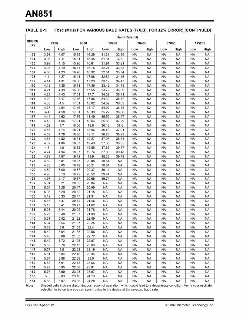
TABLE B-1: FOSC (MHZ) FOR VARIOUS BAUD RATES (F(X,B), FOR ±2% ERROR) (CONTINUED)
SPBRG(X)
Baud Rate (B)
2400 9600 19200 38400 57600 115200
Low High Low High Low High Low High Low High Low High
Note: Shaded cells indicate discontinuous region of operation, which could lead to a degenerate condition. Verify your oscillator selection to be certain you can synchronize to the device at the selected baud rate.
� 2002 Microchip Technology Inc. DS00851B-page 13
AN851
207 7.83 8.15 31.31 32.59 NA NA NA NA NA NA NA NA208 7.87 8.19 31.46 32.74 NA NA NA NA NA NA NA NA209 7.9 8.23 31.61 32.9 NA NA NA NA NA NA NA NA210 7.94 8.26 31.76 33.06 NA NA NA NA NA NA NA NA211 7.98 8.3 31.91 33.21 NA NA NA NA NA NA NA NA212 8.02 8.34 32.06 33.37 NA NA NA NA NA NA NA NA213 8.05 8.38 32.21 33.53 NA NA NA NA NA NA NA NA214 8.09 8.42 32.36 33.68 NA NA NA NA NA NA NA NA215 8.13 8.46 32.51 33.84 NA NA NA NA NA NA NA NA216 8.17 8.5 32.66 34 NA NA NA NA NA NA NA NA217 8.2 8.54 32.82 34.15 NA NA NA NA NA NA NA NA218 8.24 8.58 32.97 34.31 NA NA NA NA NA NA NA NA219 8.28 8.62 33.12 34.47 NA NA NA NA NA NA NA NA220 8.32 8.66 33.27 34.62 NA NA NA NA NA NA NA NA221 8.35 8.7 33.42 34.78 NA NA NA NA NA NA NA NA222 8.39 8.73 33.57 34.94 NA NA NA NA NA NA NA NA223 8.43 8.77 33.72 35.09 NA NA NA NA NA NA NA NA224 8.47 8.81 33.87 35.25 NA NA NA NA NA NA NA NA225 8.5 8.85 34.02 35.41 NA NA NA NA NA NA NA NA226 8.54 8.89 34.17 35.56 NA NA NA NA NA NA NA NA227 8.58 8.93 34.32 35.72 NA NA NA NA NA NA NA NA228 8.62 8.97 34.47 35.88 NA NA NA NA NA NA NA NA229 8.66 9.01 34.62 36.03 NA NA NA NA NA NA NA NA230 8.69 9.05 34.77 36.19 NA NA NA NA NA NA NA NA231 8.73 9.09 34.92 36.35 NA NA NA NA NA NA NA NA232 8.77 9.13 35.07 36.5 NA NA NA NA NA NA NA NA233 8.81 9.17 35.22 36.66 NA NA NA NA NA NA NA NA234 8.84 9.2 35.37 36.82 NA NA NA NA NA NA NA NA235 8.88 9.24 35.52 36.97 NA NA NA NA NA NA NA NA236 8.92 9.28 35.68 37.13 NA NA NA NA NA NA NA NA237 8.96 9.32 35.83 37.29 NA NA NA NA NA NA NA NA238 8.99 9.36 35.98 37.44 NA NA NA NA NA NA NA NA239 9.03 9.4 36.13 37.6 NA NA NA NA NA NA NA NA240 9.07 9.44 36.28 37.76 NA NA NA NA NA NA NA NA241 9.11 9.48 36.43 37.91 NA NA NA NA NA NA NA NA242 9.14 9.52 36.58 38.07 NA NA NA NA NA NA NA NA243 9.18 9.56 36.73 38.23 NA NA NA NA NA NA NA NA244 9.22 9.6 36.88 38.38 NA NA NA NA NA NA NA NA245 9.26 9.64 37.03 38.54 NA NA NA NA NA NA NA NA246 9.3 9.67 37.18 38.7 NA NA NA NA NA NA NA NA247 9.33 9.71 37.33 38.85 NA NA NA NA NA NA NA NA248 9.37 9.75 37.48 39.01 NA NA NA NA NA NA NA NA249 9.41 9.79 37.63 39.17 NA NA NA NA NA NA NA NA250 9.45 9.83 37.78 39.32 NA NA NA NA NA NA NA NA251 9.48 9.87 37.93 39.48 NA NA NA NA NA NA NA NA252 9.52 9.91 38.08 39.64 NA NA NA NA NA NA NA NA253 9.56 9.95 38.23 39.79 NA NA NA NA NA NA NA NA254 9.6 9.99 38.38 39.95 NA NA NA NA NA NA NA NA255 9.63 10.03 38.54 NA NA NA NA NA NA NA NA NA
TABLE B-1: FOSC (MHZ) FOR VARIOUS BAUD RATES (F(X,B), FOR ±2% ERROR) (CONTINUED)
SPBRG(X)
Baud Rate (B)
2400 9600 19200 38400 57600 115200
Low High Low High Low High Low High Low High Low High
Note: Shaded cells indicate discontinuous region of operation, which could lead to a degenerate condition. Verify your oscillator selection to be certain you can synchronize to the device at the selected baud rate.
DS00851B-page 14 � 2002 Microchip Technology Inc.
AN851
Software License AgreementThe software supplied herewith by Microchip Technology Incorporated (the “Company”) is intended and supplied to you, theCompany’s customer, for use solely and exclusively on Microchip products.The software is owned by the Company and/or its supplier, and is protected under applicable copyright laws. All rights arereserved. Any use in violation of the foregoing restrictions may subject the user to criminal sanctions under applicable laws, aswell as to civil liability for the breach of the terms and conditions of this license.THIS SOFTWARE IS PROVIDED IN AN “AS IS” CONDITION. NO WARRANTIES, WHETHER EXPRESS, IMPLIED OR STATU-TORY, INCLUDING, BUT NOT LIMITED TO, IMPLIED WARRANTIES OF MERCHANTABILITY AND FITNESS FOR A PARTICU-LAR PURPOSE APPLY TO THIS SOFTWARE. THE COMPANY SHALL NOT, IN ANY CIRCUMSTANCES, BE LIABLE FORSPECIAL, INCIDENTAL OR CONSEQUENTIAL DAMAGES, FOR ANY REASON WHATSOEVER.
APPENDIX C: BOOTLOADER FIRMWARE
C.1 PIC18F Bootloader Firmware; *****************************************************************************; ; Bootloader for PIC18F by Ross Fosler ; 03/01/2002 ... First full implementation; 03/07/2002 Changed entry method to use last byte of EEDATA.; Also removed all possible infinite loops w/ clrwdt.; 03/07/2002 Added code for direct boot entry. I.E. boot vector.; 03/09/2002 Changed the general packet format, removed the LEN field.; 03/09/2002 Modified the erase command to do multiple row erase.; 03/12/2002 Fixed write problem to CONFIG area. Write was offset by a byte.; 03/15/2002 Added work around for 18F8720 tblwt*+ problem.; 03/20/2002 Modified receive & parse engine to vector to autobaud on a checksum ; error since a checksum error could likely be a communications problem.; 03/22/2002 Removed clrwdt from the startup. This instruction affects the TO and ; PD flags. Removing this instruction should have no affect on code ; operation since the WDT is cleared on a reset and boot entry is always; on a reset.; 03/22/2002 Modified the protocol to incorporate the autobaud as part of the ; first received <STX>. Doing this improves robustness by allowing; re-sync under any condition. Previously it was possible to enter a ; state where only a hard reset would allow re-syncing.;; Memory Map; -----------------; | 0x0000 |; | 0x0002 | Boot vector; | 0x0004 | Unlock & write vector; | |; | Boot Block | (this program); | |; | 0x0200 | Re-mapped Reset Vector; | 0x0208 | Re-mapped High Priority Interrupt Vector; | 0x0218 | Re-mapped Low Priority Interrupt Vector; | | |; | |; | |; | Code Space | User program space; | |; | | |; | |; | 0xXXXXXX |; -----------------;;
� 2002 Microchip Technology Inc. DS00851B-page 15
AN851
; Incoming data format:;; <STX><STX><DATA><CHKSUM><ETX>; / \; ________/ \____________________________; / \; <COMMAND><DLEN><ADDRL><ADDRH><ADDRU><DATA>...;; Definitions:;; STX - Start of packet indicator; ETX - End of packet indicator; LEN - Length of incoming packet; DATA - General data up to 255 bytes; CHKSUM - The 8-bit two's compliment sum of LEN & DATA; COMMAND - Base command; DLEN - Length of data associated to the command; ADDR - Address up to 24 bits; DATA - Data (if any);;; Commands:;; RD_VER 0x00 Read Version Information; RD_MEM 0x01 Read Program Memory; WR_MEM 0x02 Write Program Memory; ER_MEM 0x03 Erase Program Memory; RD_EE 0x04 Read EEDATA Memory ; WR_EE 0x05 Write EEDATA Memory ; RD_CONFIG 0x06 Read Config Memory ; WT_CONFIG 0x07 Write Config Memory ;; *****************************************************************************; *****************************************************************************; #include P18F452.INC ; Standard include
#include P18F8720.inc; *****************************************************************************
; *****************************************************************************#define MINOR_VERSION 0x09 ; Version#define MAJOR_VERSION 0x00
#define RC_DLE 0x01#define RC_STX 0x02
#define STX 0x0F#define ETX 0x04#define DLE 0x05
#define TBLWT_BUG ; Timing bug found in some PIC18Fxx20s; *****************************************************************************
; *****************************************************************************CHKSUM equ 0x00 ; Checksum accumulatorCOUNTER equ 0x01 ; General counterABTIME_H equ 0x02ABTIME_L equ 0x03RXDATA equ 0x04
DS00851B-page 16 � 2002 Microchip Technology Inc.
AN851
TXDATA equ 0x05; Frame Format;; <STX><STX>[<COMMAND><DATALEN><ADDRL><ADDRH><ADDRU><...DATA...>]<CHKSUM><ETX>
DATA_BUFF equ 0x08 ; Start of receive buffer
COMMAND equ 0x08 ; Data mapped in receive bufferDATA_COUNT equ 0x09ADDRESS_L equ 0x0AADDRESS_H equ 0x0BADDRESS_U equ 0x0CPACKET_DATAequ 0x0D; *****************************************************************************
; *****************************************************************************pmwtpi macro ; tblwt*+ macro for PIC18Fxx20 bug IFDEF TBLWT_BUG
tblwt*tblrd*+
ELSEtblwt*+
ENDIFendm
; *****************************************************************************
; *****************************************************************************ORG 0x0000 ; Re-map Reset vectorbra Setupbra BootModebra StartWritebra WriteWaitEEData
ORG 0x0008VIntH
bra RVIntH ; Re-map Interrupt vector
ORG 0x0018VIntL
bra RVIntL ; Re-map Interrupt vector; *****************************************************************************
; *****************************************************************************; Setup the appropriate registers.Setup
clrf EECON1setf EEADR ; Point to last locationsetf EEADRHbsf EECON1, RD ; Read the control codeincfsz EEDATA, Wbra RVReset ; If not 0xFF then normal resetbcf TRISC, 6 ; Setup tx pin
; bsf TRISC, 7 ; Setup rx pinmovlw b'10010000' ; Setup rx and txmovwf CSTA1movlw b'00100110'movwf TXSTA1
; *****************************************************************************
� 2002 Microchip Technology Inc. DS00851B-page 17
AN851
; *****************************************************************************Autobaud;; ___ __________ _________; \__/ \__________/; | |; |-------- p ----------|;; p = The number of instructions between the first and last; rising edge of the RS232 control sequence 0x0F. : Other possible control sequences are 0x01, 0x03, 0x07, 0x1F,; 0x3F, 0x7F.;; SPBRG = (p / 32) - 1, BRGH = 1bcf RCSTA1, CREN ; Stop receivingmovlw b'00000011' ; x16 Prescalemovwf T0CONclrf TMR0H ; Reset timerclrf TMR0Lrcall WaitForRise
bsf T0CON, TMR0ON ; Start countingrcall WaitForRisebcf T0CON, TMR0ON ; Stop countingmovff TMR0L, ABTIME_L ; Read the timer
DivB32rrcf TMR0H, F ; divide by 2rrcf ABTIME_L, Fbtfss STATUS, C ; Roundingdecf ABTIME_L, Fmovff ABTIME_L, SPBRG1 ; Syncbsf RCSTA1, CREN ; Start receivingmovf RCREG1, W ; Empty the buffermovf RCREG1, W
; *****************************************************************************
; *****************************************************************************; Read and parse the data.StartOfLine
rcall RdRS232 ; Get second <STX>xorlw STXbnz Autobaud ; Otherwise go back for another characterlfsr 0, DATA_BUFF ; Point to the bufferclrf CHKSUM ; Reset checksumclrf COUNTER ; Reset buffer count
GetNextDatrcall RdRS232 ; Get the dataxorlw STX ; Check for a STXbz StartOfLine ; Yes, start over
NoSTXmovf RXDATA, Wxorlw ETX ; Check for a ETXbz CheckSum ; Yes, examine checksum
NoETXmovf RXDATA, Wxorlw DLE ; Check for a DLEbnz NoDLErcall RdRS232 ; Yes, Get the next byte
NoDLEmovf RXDATA, Waddwf CHKSUM, F ; Get summovwf POSTINC0 ; Store the datadcfsnz COUNTER, F ; Limit buffer to 256 bytes
DS00851B-page 18 � 2002 Microchip Technology Inc.
AN851
bra Autobaudbra GetNextDatCheckSummovf CHKSUM ; Checksum testbnz Autobaud
; ***********************************************
; ***********************************************; Pre-setup, common to all commands.
movf ADDRESS_L, W ; Set all possible pointersmovwf TBLPTRLmovwf EEADRmovf ADDRESS_H, Wmovwf TBLPTRHmovwf EEADRHmovff ADDRESS_U, TBLPTRUlfsr FSR0, PACKET_DATAmovf DATA_COUNT, W ; Setup countermovwf COUNTERbtfsc STATUS, Zreset ; Non valid count (Special Command)
; ***********************************************
; ***********************************************; Test the command field and sub-command.CheckCommand
movf COMMAND, W ; Test for a valid commandsublw d'7'bnc Autobaudclrf PCLATH ; Setup for a calculated jumpclrf PCLATUrlncf COMMAND, W ; Jumpaddwf PCL, Fbra ReadVersionbra ReadProgMembra WriteProgMembra EraseProgMembra ReadEEbra WriteEEbra ReadProgMem ;ReadConfigbra WriteConfig
; ***********************************************
; ***********************************************; Commands; ; In: <STX><STX>[<0x00><0x02>]<0xFF><ETX>; OUT: <STX><STX>[<0x00><0x02><VERL><VERH>]<CHKSUM><ETX>
ReadVersionmovlw MINOR_VERSIONmovwf DATA_BUFF + 2movlw MAJOR_VERSIONmovwf DATA_BUFF + 3movlw 0x04bra WritePacket
; In: <STX><STX>[<0x01><DLEN><ADDRL><ADDRH><ADDRU>]<CHKSUM><ETX>; OUT: <STX><STX>[<0x01><DLEN><ADDRL><ADDRH><ADDRU><DATA>...]<CHKSUM><ETX>
� 2002 Microchip Technology Inc. DS00851B-page 19
AN851
ReadProgMemtblrd *+ ; Fill buffermovff TABLAT, POSTINC0decfsz COUNTER, Fbra ReadProgMem ; Not finished then repeatmovf DATA_COUNT, W ; Setup packet lengthaddlw 0x05bra WritePacket
; In: <STX><STX>[<0x02><DLENBLOCK><ADDRL><ADDRH><ADDRU><DATA>...]<CHKSUM><ETX>; OUT: <STX><STX>[<0x02>]<CHKSUM><ETX>
WriteProgMemmovlw b'11111000' ; Force a boundryandwf TBLPTRL, Fmovlw 0x08
Lp1movff POSTINC0, TABLAT ; Load the holding registerspmwtpi ; Same as tblwt *+decfsz WREG, Fbra Lp1tblrd *- ; Point back into the blockmovlw b'10000100' ; Setup writesmovwf EECON1rcall StartWrite ; Write the datatblrd *+ ; Point to the beginning of the next blockdecfsz COUNTER, Fbra WriteProgMem ; Not finished then repeatbra SendAcknowledge ; Send acknowledge
; In:<STX><STX>[<0x03><DLENROW><ADDRL><ADDRH><ADDRL>]<CHKSUM><ETX>; OUT:<STX><STX>[<0x03>]<CHKSUM><ETX>
EraseProgMemmovlw b'10010100' ; Setup writesmovwf EECON1rcall StartWrite ; Erase the rowmovlw 0x40 ; Point to next rowaddwf TBLPTRL, Fclrf WREGaddwfc TBLPTRH, Faddwfc TBLPTRU, Fdecfsz COUNTER, Fbra EraseProgMembra SendAcknowledge ; Send acknowledge
; In:<STX><STX>[<0x04><DLEN><ADDRL><ADDRH><0x00>]<CHKSUM><ETX>; OUT:<STX><STX>[<0x04><DLEN><ADDRL><ADDRH><0x00><DATA>...]<CHKSUM><ETX>
ReadEEclrf EECON1 bsf EECON1, RD ; Read the datamovff EEDATA, POSTINC0infsnz EEADR, F; Adjust EEDATA pointerincf EEADRH, Fdecfsz COUNTER, Fbra ReadEE ; Not finished then repeatmovf DATA_COUNT, W ; Setup packet lengthaddlw 0x05bra WritePacket
; In: <STX><STX>[<0x05><DLEN><ADDRL><ADDRH><0x00><DATA>...]<CHKSUM><ETX>; OUT: <STX><STX>[<0x05>]<CHKSUM><ETX>
DS00851B-page 20 � 2002 Microchip Technology Inc.
AN851
WriteEEmovff POSTINC0, EEDATArcall WriteWaitEEData ; Write datainfsnz EEADR, F ; Adjust EEDATA pointerincf EEADRH, Fdecfsz COUNTER, Fbra WriteEE ; Not finished then repeatbra SendAcknowledge ; Send acknowledge
; In: <STX><STX>[<0x06><DLEN><ADDRL><ADDRH><ADDRU>]<CHKSUM><ETX>; OUT: <STX><STX>[<0x06><DLEN><ADDRL><ADDRH><ADDRU><DATA>...]<CHKSUM><ETX>
;ReadConfig; movlw b'11000000'; movwf EECON1;;Lp5
tblrd*+; movff TABLAT, POSTINC0; decfsz COUNTER, F; bra Lp5 ; Not finished then repeat; movf DATA_COUNT, W ; Setup packet length; addlw 0x05; bra WritePacket
; In: <STX><STX>[<0x07><DLEN><ADDRL><ADDRH><ADDRU><DATA>...]<CHKSUM><ETX>; OUT: <STX><STX>[<0x07>]<CHKSUM><ETX>
WriteConfigmovlw b'11000100'movwf EECON1movff POSTINC0, TABLAT ; Write to config areatblwt *rcall StartWritetblrd *+decfsz COUNTER, Fbra WriteConfig ; Not finished then repeatbra SendAcknowledge ; Send acknowledge
; ***********************************************
; ***********************************************; Send the data buffer back.;; <STX><STX>[<DATA>...]<CHKSUM><ETX>
SendAcknowledgemovlw 0x01 ; Send acknowledge
WritePacketmovwf COUNTERmovlw STX ; Send start conditionrcall WrRS232rcall WrRS232clrf CHKSUM ; Reset checksumlfsr FSR0, DATA_BUFF ; Setup pointer to buffer area
SendNext ; Send DATAmovf POSTINC0, Waddwf CHKSUMrcall WrDatadecfsz COUNTER, Fbra SendNextnegf CHKSUM ; Send checksummovf CHKSUM, Wrcall WrData
� 2002 Microchip Technology Inc. DS00851B-page 21
AN851
movlw ETX ; Send stop conditionrcall WrRS232bra Autobaud; *****************************************************************************
; *****************************************************************************; Write a byte to the serial port.WrData
movwf TXDATA ; Save the dataxorlw STX ; Check for a STXbz WrDLE ; No, continue WrNextmovf TXDATA, Wxorlw ETX ; Check for a ETXbz WrDLE ; No, continue WrNextmovf TXDATA, Wxorlw DLE ; Check for a DLEbnz WrNext ; No, continue WrNext
WrDLEmovlw DLE ; Yes, send DLE firstrcall WrRS232
WrNextmovf TXDATA, W ; Then send STX
WrRS232clrwdtbtfss PIR1, TXIF ; Write only if TXREG is readybra $ - 2movwf TXREG1 ; Start sendingreturn
; *****************************************************************************
; *****************************************************************************RdRS232
clrwdtbtfsc RCSTA1, OERR ; Reset on overrunresetbtfss PIR1, RCIF ; Wait for data from RS232bra $ - 2movf RCREG1, W ; Save the datamovwf RXDATAreturn
; *****************************************************************************
; *****************************************************************************BootMode
setf EEADR ; Point to the last bytesetf EEADRHsetf EEDATA ; Bootmode control bytercall WriteWaitEEDatareset
; *****************************************************************************
; *****************************************************************************WaitForRise
btfsc PORTC, 7 ; Wait for a falling edgebra WaitForRiseclrwdt
DS00851B-page 22 � 2002 Microchip Technology Inc.
AN851
WtSRbtfss PORTC, 7 ; Wait for starting edgebra WtSRreturn
; *****************************************************************************
; *****************************************************************************; Unlock and start the write or erase sequence.
StartWriteclrwdtmovlw 0x55 ; Unlockmovwf EECON2movlw 0xAAmovwf EECON2bsf EECON1, WR ; Start the writenopreturn
; *****************************************************************************
; *****************************************************************************ORG 0x000A
WriteWaitEEDatamovlw b'00000100' ; Setup for EEDatamovwf EECON1rcall StartWritebtfsc EECON1, WR ; Write and waitbra $ - 2return
; *****************************************************************************
; *****************************************************************************ORG 0x200
RVReset
ORG 0x208RVIntH
ORG 0x218RVIntL; *****************************************************************************
END
� 2002 Microchip Technology Inc. DS00851B-page 23
AN851
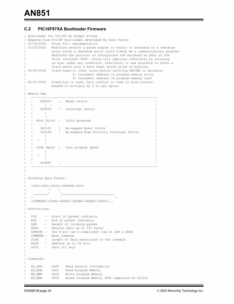
C.2 PIC16F87XA Bootloader Firmware; Bootloader for PIC16F by Rodger Richey; Adapted from PIC18F bootloader developed by Ross Fosler; 03/18/2002 First full implementation; 03/25/2002 Modified receive & parse engine to vector to autobaud on a checksum ; error since a checksum error could likely be a communications problem.; Modified the protocol to incorporate the autobaud as part of the ; first received <STX>. Doing this improves robustness by allowing; re-sync under any condition. Previously it was possible to enter a ; state where only a hard reset would allow re-syncing.; 04/09/2002 Fixed bugs:1) clear carry before shifting ABTIME in Autobaud; 2) Increment address in program memory write; 3) Increment address in program memory read; 06/07/2002 Fixed bug in read, byte counter in code is word counter. ; Needed to multiply by 2 to get bytes.;; Memory Map; ---------------------------------------------------------------------; | 0x0000 | Reset vector |; | | | |; | 0x0004 | Interrupt vector |; | | |; | | |; | Boot Block | (this program) |; | | |; | 0x0100 | Re-mapped Reset Vector |; | 0x0104 | Re-mapped High Priority Interrupt Vector |; | | |; | | | |; | | |; | Code Space | User program space |; | | |; | | | |; | | |; | 0x3FFF | |; ---------------------------------------------------------------------;;; Incoming data format:;; <STX><STX><DATA><CHKSUM><ETX>; / \; ________/ \____________________________; / \; <COMMAND><DLEN><ADDRL><ADDRH><ADDRU><DATA>...;; Definitions:;; STX - Start of packet indicator; ETX - End of packet indicator; LEN - Length of incoming packet; DATA - General data up to 255 bytes; CHKSUM - The 8-bit two's compliment sum of LEN & DATA; COMMAND - Base command; DLEN - Length of data associated to the command; ADDR - Address up to 24 bits; DATA - Data (if any);;; Commands:;; RD_VER 0x00 Read Version Information; RD_MEM 0x01 Read Program Memory; WR_MEM 0x02 Write Program Memory; ER_MEM 0x03 Erase Program Memory (NOT supported by PIC16)DS00851B-page 24 � 2002 Microchip Technology Inc.
AN851
; RD_EE 0x04 Read EEDATA Memory ; WR_EE 0x05 Write EEDATA Memory ; RD_CONFIG 0x06 Read Config Memory (NOT supported by PIC16); WT_CONFIG 0x07 Write Config Memory (NOT supported by PIC16);; *****************************************************************************; *****************************************************************************#include P16F877A.INC; Standard include
; *****************************************************************************
errorlevel -302; Do not show any banking warnings
; *****************************************************************************#define MINOR_VERSION 0x03 ; Version#define MAJOR_VERSION 0x00
#define RC_DLE 0x01#define RC_STX 0x02
#define STX 0x0F#define ETX 0x04#define DLE 0x05
;#define DEBUGGING ; Debugging enabled with ICD; *****************************************************************************
; *****************************************************************************CHKSUM equ 0x71 ; Checksum accumulatorCOUNTER equ 0x72 ; General counterABTIME equ 0x73RXDATA equ 0x74TXDATA equ 0x75TEMP equ 0x76
PCLATH_TEMPequ 0x7D ; Interrupt contextSTATUS_TEMPequ 0x7E ; save/restore registersW_TEMP equ 0x7F
; Frame Format;; <STX><STX>[<COMMAND><DATALEN><ADDRL><ADDRH><ADDRU><...DATA...>]<CHKSUM><ETX>
DATA_BUFFequ0x10; Start of receive buffer
COMMAND equ 0x10 ; Data mapped in receive bufferDATA_COUNT equ 0x11ADDRESS_L equ 0x12ADDRESS_H equ 0x13ADDRESS_U equ 0x14PACKET_DATAequ 0x15; *****************************************************************************
; *****************************************************************************ORG 0x0000 ; Re-map Reset vector
VResetbcf STATUS,RP0bsf STATUS,RP1clrf PCLATH
� 2002 Microchip Technology Inc. DS00851B-page 25
AN851
goto SetupORG 0x0004VIntmovwf W_TEMPswapf STATUS,Wmovwf STATUS_TEMPclrf STATUSmovf PCLATH,Wmovwf PCLATH_TEMPclrf PCLATHgoto RVInt ; Re-map Interrupt vector
; *****************************************************************************
; *****************************************************************************; Set up the appropriate registers.Setup
clrwdtmovlw 0xFFmovwf EEADR ; Point to last locationbsf STATUS,RP0clrf EECON1bsf EECON1,RD ; Read the control codebcf STATUS,RP0incf EEDATA,Wbtfsc STATUS,Zgoto SRXbcf STATUS,RP1goto RVReset ; If not 0xFF then normal reset
SRXbcf STATUS,RP1movlw b'10000000' ; Setup rx and tx, CREN disabled;movwf RCSTAbsf STATUS,RP0bcf TRISC,6 ; Setup tx pinmovlw b'00100110'movwf TXSTAbsf STATUS,IRP
; *****************************************************************************
; *****************************************************************************Autobaud;; ___ __________ ________; \__/ \__________/; | |; |-------- p ----------|;; p = The number of instructions between the first and last; rising edge of the RS232 control sequence 0x0F. Other ; possible control sequences are 0x01, 0x03, 0x07, 0x1F, ; 0x3F, 0x7F.;; SPBRG = (p / 32) - 1 BRGH = 1
bcf STATUS,RP1bsf STATUS,RP0movlw b'00000011'movwf OPTION_REGbcf STATUS,RP0bcf RCSTA,CRENcall WaitForRise
DS00851B-page 26 � 2002 Microchip Technology Inc.
AN851
clrf TMR0 ; Start countingcall WaitForRisemovf TMR0,W ; Read the timermovwf ABTIMEbcf STATUS,Crrf ABTIME,Wbtfss STATUS,C ; Roundingaddlw 0xFFbsf STATUS,RP0movwf SPBRGbcf STATUS,RP0bsf RCSTA,CREN ; Enable receivemovf RCREG,Wmovf RCREG,Wbsf STATUS,RP0movlw b'11111111'movwf OPTION_REG; *****************************************************************************
; *****************************************************************************; Read and parse the data.StartOfLine
bcf STATUS,RP0bcf STATUS,RP1call RdRS232 ; Look for a start of linexorlw STX ; <STX><STX>btfss STATUS,Zgoto Autobaud ; was StartOflinemovlw DATA_BUFF ; Point to the buffermovwf FSRclrf CHKSUM ; Reset checksum
GetNextDatcall RdRS232 ; Get the dataxorlw STX ; Check for a STXbtfsc STATUS,Zgoto StartOfLine ; Yes, start over
NoSTXmovf RXDATA,Wxorlw ETX ; Check for a ETXbtfsc STATUS,Zgoto CheckSum ; Yes, examine checksum
NoETXmovf RXDATA,Wxorlw DLE ; Check for a DLEbtfss STATUS,Zgoto NoDLE ; Check for a DLEcall RdRS232 ; Yes, Get the next byte
NoDLEmovf RXDATA,Wmovwf INDF ; Store the dataaddwf CHKSUM,F ; Get sumincf FSR,Fgoto GetNextDat
CheckSummovf CHKSUM,F ; Checksum testbtfss STATUS,Zgoto Autobaud
; ***********************************************
� 2002 Microchip Technology Inc. DS00851B-page 27
AN851
; ***********************************************; Pre-setup, common to all commands.
bsf STATUS,RP1movf ADDRESS_L,W ; Set all possible pointersmovwf EEADRmovf ADDRESS_H,Wmovwf EEADRHmovlw PACKET_DATAmovwf FSRmovf DATA_COUNT,W ; Setup countermovwf COUNTERbtfsc STATUS,Zgoto VReset ; Non valid count (Special Command)
; ***********************************************
; ***********************************************; Test the command field and sub-command.CheckCommand
movf COMMAND,W ; Test for a valid commandsublw d'7'btfss STATUS,Cgoto Autobaudmovf COMMAND,W ; Perform calculated jumpaddwf PCL,Fgoto ReadVersion ; 0goto ReadProgMem ; 1goto WriteProgMem ; 2goto StartOfLine ; 3goto ReadEE ; 4goto WriteEE ; 5goto StartOfLine ; 6goto StartOfLine ; 7
;maybe add jump to reset vector in this table; ***********************************************
; ***********************************************; Commands; ; In: <STX><STX>[<0x00><0x02>]<0xFF><ETX>; OUT: <STX><STX>[<0x00><VERL><VERH>]<CHKSUM><ETX>ReadVersion
movlw MINOR_VERSIONmovwf DATA_BUFF + 2movlw MAJOR_VERSIONmovwf DATA_BUFF + 3movlw 0x04goto WritePacket
; In: <STX><STX>[<0x01><DLEN><ADDRL><ADDRH><ADDRU>]<CHKSUM><ETX>; OUT: <STX><STX>[<0x01><DLEN><ADDRL><ADDRH><ADDRU><DATA>...]<CHKSUM><ETX>ReadProgMemRPM1
bsf STATUS,RP0bsf EECON1,EEPGDbsf EECON1,RDnopnopbcf STATUS,RP0movf EEDATA,Wmovwf INDF
DS00851B-page 28 � 2002 Microchip Technology Inc.
AN851
incf FSR,Fmovf EEDATH,Wmovwf INDFincf FSR,Fincf EEADR,Fbtfsc STATUS,Zincf EEADRH,Fdecfsz COUNTER,Fgoto RPM1 ; Not finished then repeatrlf DATA_COUNT,W ; Setup packet lengthaddlw 0x05goto WritePacket; In: <STX><STX>[<0x02><DLENBLOCK><ADDRL><ADDRH><ADDRU><DATA>...]<CHKSUM><ETX>; OUT: <STX><STX>[<0x02>]<CHKSUM><ETX>
WriteProgMembsf STATUS,RP0movlw b'10000100' ; Setup writesmovwf EECON1bcf STATUS,RP0movlw b'11111100' ; Force a boundryandwf EEADR,Fmovlw 0x04movwf TEMP
Lp1movf INDF,Wmovwf EEDATAincf FSR,Fmovf INDF,Wmovwf EEDATHincf FSR,Fcall StartWriteincf EEADR,Fbtfsc STATUS,Zincf EEADRH,Fdecfsz TEMP,Fgoto Lp1decfsz COUNTER,Fgoto WriteProgMem ; Not finished then repeatgoto SendAcknowledge ; Send acknowledge
; In: <STX><STX>[<0x04><DLEN><ADDRL><ADDRH><0x00>]<CHKSUM><ETX>; OUT: <STX><STX>[<0x04><DLEN><ADDRL><ADDRH><0x00><DATA>...]<CHKSUM><ETX>
ReadEEbsf STATUS,RP0clrf EECON1bsf EECON1,RD ; Read the databcf STATUS,RP0movf EEDATA,Wmovwf INDFincf FSR,Fincf EEADR,F ; Adjust EEDATA pointerdecfsz COUNTER,Fgoto ReadEE ; Not finished then repeatmovf DATA_COUNT,W ; Setup packet lengthaddlw 0x05goto WritePacket
; IN: <STX><STX>[<0x05><DLEN><ADDRL><ADDRH><0x00><DATA>...]<CHKSUM><ETX>; OUT: <STX><STX>[<0x05>]<CHKSUM><ETX>
� 2002 Microchip Technology Inc. DS00851B-page 29
AN851
WriteEEmovf INDF,Wmovwf EEDATAincf FSR,Fcall WriteWaitEEData ; Write dataincf EEADR,F ; Adjust EEDATA pointerdecfsz COUNTER,Fgoto WriteEE ; Not finished then repeatgoto SendAcknowledge ; Send acknowledge
; ***********************************************
; ***********************************************; Send the data buffer back.;; <STX><STX>[<DATA>...]<CHKSUM><ETX>
SendAcknowledgemovlw 0x01 ; Send acknowledge
WritePacketmovwf COUNTERmovlw STX ; Send start conditioncall WrRS232call WrRS232clrf CHKSUM ; Reset checksummovlw DATA_BUFF ; Setup pointer to buffer areamovwf FSR
SendNext ; Send DATAmovf INDF,Waddwf CHKSUM,Fincf FSR,Fcall WrDatadecfsz COUNTER,Fgoto SendNextcomf CHKSUM,W ; Send checksumaddlw 0x01call WrDatamovlw ETX ; Send stop conditioncall WrRS232goto Autobaud
; *****************************************************************************
; *****************************************************************************; Write a byte to the serial port.
WrDatamovwf TXDATA ; Save the dataxorlw STX ; Check for a STXbtfsc STATUS,Zgoto WrDLE ; No, continue WrNextmovf TXDATA,Wxorlw ETX ; Check for a ETXbtfsc STATUS,Zgoto WrDLE ; No, continue WrNextmovf TXDATA,Wxorlw DLE ; Check for a DLEbtfss STATUS,Zgoto WrNext ; No, continue WrNext
WrDLEmovlw DLE ; Yes, send DLE firstcall WrRS232
DS00851B-page 30 � 2002 Microchip Technology Inc.
AN851
WrNextmovf TXDATA,W ; Then send STX; DC
WrRS232clrwdtbcf STATUS,RP1btfss PIR1,TXIF ; Write only if TXREG is readygoto $ - 1movwf TXREG ; Start sendingreturn
; *****************************************************************************
; *****************************************************************************RdRS232
clrwdtbtfsc RCSTA,OERR ; Reset on overrungoto VResetbtfss PIR1,RCIF ; Wait for data from RS232goto $ - 1movf RCREG,W ; Save the datamovwf RXDATAreturn
; *****************************************************************************
; *****************************************************************************WaitForRise
btfsc PORTC,7 ; Wait for a falling edgegoto WaitForRiseclrwdt ; Do we need this?
WtSRbtfss PORTC,7 ; Wait for starting edgegoto WtSRreturn
; *****************************************************************************
; *****************************************************************************; Unlock and start the write or erase sequence.
StartWriteclrwdtbsf STATUS,RP0movlw 0x55 ; Unlockmovwf EECON2movlw 0xAAmovwf EECON2bsf EECON1,WR ; Start the writenopnopbcf STATUS,RP0return
; *****************************************************************************
� 2002 Microchip Technology Inc. DS00851B-page 31
AN851
; *****************************************************************************WriteWaitEEDatabsf STATUS,RP0movlw b'00000100' ; Setup for EEDatamovwf EECON1call StartWritebtfsc EECON1,WR ; Write and waitgoto $ - 1bcf STATUS,RP0return
; *****************************************************************************; *****************************************************************************
ORG 0x100RVReset
ORG 0x104RVInt
; *****************************************************************************
END
DS00851B-page 32 � 2002 Microchip Technology Inc.
AN851
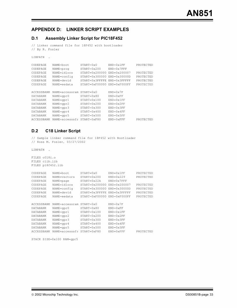
APPENDIX D: LINKER SCRIPT EXAMPLESD.1 Assembly Linker Script for PIC18F452// Linker command file for 18F452 with bootloader// By R. Fosler
LIBPATH .
CODEPAGE NAME=boot START=0x0 END=0x1FF PROTECTEDCODEPAGE NAME=prog START=0x200 END=0x7FFFCODEPAGE NAME=idlocs START=0x200000 END=0x200007 PROTECTEDCODEPAGE NAME=config START=0x300000 END=0x30000D PROTECTEDCODEPAGE NAME=devid START=0x3FFFFE END=0x3FFFFF PROTECTEDCODEPAGE NAME=eedata START=0xF00000 END=0xF000FF PROTECTED
ACCESSBANK NAME=accessram START=0x0 END=0x7FDATABANK NAME=gpr0 START=0x80 END=0xFFDATABANK NAME=gpr1 START=0x100 END=0x1FFDATABANK NAME=gpr2 START=0x200 END=0x2FFDATABANK NAME=gpr3 START=0x300 END=0x3FFDATABANK NAME=gpr4 START=0x400 END=0x4FFDATABANK NAME=gpr5 START=0x500 END=0x5FFACCESSBANK NAME=accesssfr START=0xF80 END=0xFFF PROTECTED
D.2 C18 Linker Script// Sample linker command file for 18F452 with Bootloader// Ross M. Fosler, 03/27/2002
LIBPATH .
FILES c018i.oFILES clib.libFILES p18f452.lib
CODEPAGE NAME=boot START=0x0 END=0x1FF PROTECTEDCODEPAGE NAME=vectors START=0x200 END=0x229 PROTECTEDCODEPAGE NAME=page START=0x22A END=0x7FFFCODEPAGE NAME=idlocs START=0x200000 END=0x200007 PROTECTEDCODEPAGE NAME=config START=0x300000 END=0x30000D PROTECTEDCODEPAGE NAME=devid START=0x3FFFFE END=0x3FFFFF PROTECTEDCODEPAGE NAME=eedata START=0xF00000 END=0xF000FF PROTECTED
ACCESSBANK NAME=accessram START=0x0 END=0x7FDATABANK NAME=gpr0 START=0x80 END=0xFFDATABANK NAME=gpr1 START=0x100 END=0x1FFDATABANK NAME=gpr2 START=0x200 END=0x2FFDATABANK NAME=gpr3 START=0x300 END=0x3FFDATABANK NAME=gpr4 START=0x400 END=0x4FFDATABANK NAME=gpr5 START=0x500 END=0x5FFACCESSBANK NAME=accesssfr START=0xF80 END=0xFFF PROTECTED
STACK SIZE=0x100 RAM=gpr5
� 2002 Microchip Technology Inc. DS00851B-page 33
AN851
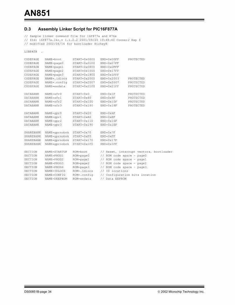
D.3 Assembly Linker Script for PIC16F877A// Sample linker command file for 16F877a and 876a// $Id: 16f877a.lkr,v 1.1.2.2 2001/09/20 19:48:40 ConnerJ Exp $// modified 2002/06/14 for bootloader RicheyRLIBPATH .
CODEPAGE NAME=boot START=0x0000 END=0x00FF PROTECTEDCODEPAGE NAME=page0 START=0x0100 END=0x07FFCODEPAGE NAME=page1 START=0x0800 END=0x0FFFCODEPAGE NAME=page2 START=0x1000 END=0x17FFCODEPAGE NAME=page3 START=0x1800 END=0x1FFFCODEPAGE NAME=.idlocs START=0x2000 END=0x2003 PROTECTEDCODEPAGE NAME=.config START=0x2007 END=0x2007 PROTECTEDCODEPAGE NAME=eedata START=0x2100 END=0x21FF PROTECTED
DATABANK NAME=sfr0 START=0x0 END=0x1F PROTECTEDDATABANK NAME=sfr1 START=0x80 END=0x9F PROTECTEDDATABANK NAME=sfr2 START=0x100 END=0x10F PROTECTEDDATABANK NAME=sfr3 START=0x180 END=0x18F PROTECTED
DATABANK NAME=gpr0 START=0x20 END=0x6FDATABANK NAME=gpr1 START=0xA0 END=0xEFDATABANK NAME=gpr2 START=0x110 END=0x16FDATABANK NAME=gpr3 START=0x190 END=0x1EF
SHAREBANK NAME=gprnobnk START=0x70 END=0x7FSHAREBANK NAME=gprnobnk START=0xF0 END=0xFFSHAREBANK NAME=gprnobnk START=0x170 END=0x17FSHAREBANK NAME=gprnobnk START=0x1F0 END=0x1FF
SECTION NAME=STARTUP ROM=boot // Reset, interrupt vectors, bootloaderSECTION NAME=PROG1 ROM=page0 // ROM code space - page0SECTION NAME=PROG2 ROM=page1 // ROM code space - page1SECTION NAME=PROG3 ROM=page2 // ROM code space - page2SECTION NAME=PROG4 ROM=page3 // ROM code space - page3SECTION NAME=IDLOCS ROM=.idlocs // ID locationsSECTION NAME=CONFIG ROM=.config // Configuration bits locationSECTION NAME=DEEPROM ROM=eedata // Data EEPROM
DS00851B-page 34 � 2002 Microchip Technology Inc.
AN851
APPENDIX E: SOFTWAREDISCUSSED IN THIS APPLICATION NOTE
All of the software covered in this application note (thePIC16/PIC18 Quick Programmer, the source code forthe bootloaders and associated project files) are avail-able as a single WinZip archive file. The archive maybe downloaded from the Microchip corporate web siteat:
www.microchip.com
� 2002 Microchip Technology Inc. DS00851B-page 35
AN851
NOTES:DS00851B-page 36 � 2002 Microchip Technology Inc.
Note the following details of the code protection feature on PICmicro® MCUs.
• The PICmicro family meets the specifications contained in the Microchip Data Sheet.• Microchip believes that its family of PICmicro microcontrollers is one of the most secure products of its kind on the market today,
when used in the intended manner and under normal conditions.• There are dishonest and possibly illegal methods used to breach the code protection feature. All of these methods, to our knowl-
edge, require using the PICmicro microcontroller in a manner outside the operating specifications contained in the data sheet. The person doing so may be engaged in theft of intellectual property.
• Microchip is willing to work with the customer who is concerned about the integrity of their code.• Neither Microchip nor any other semiconductor manufacturer can guarantee the security of their code. Code protection does not
mean that we are guaranteeing the product as “unbreakable”.• Code protection is constantly evolving. We at Microchip are committed to continuously improving the code protection features of
our product.If you have any further questions about this matter, please contact the local sales office nearest to you.
Information contained in this publication regarding deviceapplications and the like is intended through suggestion onlyand may be superseded by updates. It is your responsibility toensure that your application meets with your specifications.No representation or warranty is given and no liability isassumed by Microchip Technology Incorporated with respectto the accuracy or use of such information, or infringement ofpatents or other intellectual property rights arising from suchuse or otherwise. Use of Microchip’s products as critical com-ponents in life support systems is not authorized except withexpress written approval by Microchip. No licenses are con-veyed, implicitly or otherwise, under any intellectual propertyrights.
� 2002 Microchip Technology Inc.
Trademarks
The Microchip name and logo, the Microchip logo, KEELOQ,MPLAB, PIC, PICmicro, PICSTART and PRO MATE areregistered trademarks of Microchip Technology Incorporatedin the U.S.A. and other countries.
FilterLab, microID, MXDEV, MXLAB, PICMASTER, SEEVALand The Embedded Control Solutions Company areregistered trademarks of Microchip Technology Incorporatedin the U.S.A.
dsPIC, dsPICDEM.net, ECONOMONITOR, FanSense,FlexROM, fuzzyLAB, In-Circuit Serial Programming, ICSP,ICEPIC, microPort, Migratable Memory, MPASM, MPLIB,MPLINK, MPSIM, PICC, PICDEM, PICDEM.net, rfPIC, SelectMode and Total Endurance are trademarks of MicrochipTechnology Incorporated in the U.S.A. and other countries.
Serialized Quick Turn Programming (SQTP) is a service markof Microchip Technology Incorporated in the U.S.A.
All other trademarks mentioned herein are property of theirrespective companies.
© 2002, Microchip Technology Incorporated, Printed in theU.S.A., All Rights Reserved.
Printed on recycled paper.
DS00851B - page 37
Microchip received QS-9000 quality system certification for its worldwide headquarters, design and wafer fabrication facilities in Chandler and Tempe, Arizona in July 1999 and Mountain View, California in March 2002. The Company’s quality system processes and procedures are QS-9000 compliant for its PICmicro® 8-bit MCUs, KEELOQ® code hopping devices, Serial EEPROMs, microperipherals, non-volatile memory and analog products. In addition, Microchip’s quality system for the design and manufacture of development systems is ISO 9001 certified.
DS00851B-page 38 � 2002 Microchip Technology Inc.
AMERICASCorporate Office2355 West Chandler Blvd.Chandler, AZ 85224-6199Tel: 480-792-7200 Fax: 480-792-7277Technical Support: 480-792-7627Web Address: http://www.microchip.comRocky Mountain2355 West Chandler Blvd.Chandler, AZ 85224-6199Tel: 480-792-7966 Fax: 480-792-4338
Atlanta500 Sugar Mill Road, Suite 200BAtlanta, GA 30350Tel: 770-640-0034 Fax: 770-640-0307Boston2 Lan Drive, Suite 120Westford, MA 01886Tel: 978-692-3848 Fax: 978-692-3821Chicago333 Pierce Road, Suite 180Itasca, IL 60143Tel: 630-285-0071 Fax: 630-285-0075Dallas4570 Westgrove Drive, Suite 160Addison, TX 75001Tel: 972-818-7423 Fax: 972-818-2924DetroitTri-Atria Office Building 32255 Northwestern Highway, Suite 190Farmington Hills, MI 48334Tel: 248-538-2250 Fax: 248-538-2260Kokomo2767 S. Albright Road Kokomo, Indiana 46902Tel: 765-864-8360 Fax: 765-864-8387Los Angeles18201 Von Karman, Suite 1090Irvine, CA 92612Tel: 949-263-1888 Fax: 949-263-1338New York150 Motor Parkway, Suite 202Hauppauge, NY 11788Tel: 631-273-5305 Fax: 631-273-5335San JoseMicrochip Technology Inc.2107 North First Street, Suite 590San Jose, CA 95131Tel: 408-436-7950 Fax: 408-436-7955Toronto6285 Northam Drive, Suite 108Mississauga, Ontario L4V 1X5, CanadaTel: 905-673-0699 Fax: 905-673-6509
ASIA/PACIFICAustraliaMicrochip Technology Australia Pty LtdSuite 22, 41 Rawson StreetEpping 2121, NSWAustraliaTel: 61-2-9868-6733 Fax: 61-2-9868-6755China - BeijingMicrochip Technology Consulting (Shanghai)Co., Ltd., Beijing Liaison OfficeUnit 915Bei Hai Wan Tai Bldg.No. 6 Chaoyangmen Beidajie Beijing, 100027, No. ChinaTel: 86-10-85282100 Fax: 86-10-85282104China - ChengduMicrochip Technology Consulting (Shanghai)Co., Ltd., Chengdu Liaison OfficeRm. 2401, 24th Floor, Ming Xing Financial TowerNo. 88 TIDU StreetChengdu 610016, ChinaTel: 86-28-86766200 Fax: 86-28-86766599China - FuzhouMicrochip Technology Consulting (Shanghai)Co., Ltd., Fuzhou Liaison OfficeUnit 28F, World Trade PlazaNo. 71 Wusi RoadFuzhou 350001, ChinaTel: 86-591-7503506 Fax: 86-591-7503521China - ShanghaiMicrochip Technology Consulting (Shanghai)Co., Ltd.Room 701, Bldg. BFar East International PlazaNo. 317 Xian Xia RoadShanghai, 200051Tel: 86-21-6275-5700 Fax: 86-21-6275-5060China - ShenzhenMicrochip Technology Consulting (Shanghai)Co., Ltd., Shenzhen Liaison OfficeRm. 1315, 13/F, Shenzhen Kerry Centre,Renminnan LuShenzhen 518001, ChinaTel: 86-755-82350361 Fax: 86-755-82366086China - Hong Kong SARMicrochip Technology Hongkong Ltd.Unit 901-6, Tower 2, Metroplaza223 Hing Fong RoadKwai Fong, N.T., Hong KongTel: 852-2401-1200 Fax: 852-2401-3431IndiaMicrochip Technology Inc.India Liaison OfficeDivyasree Chambers1 Floor, Wing A (A3/A4)No. 11, O’Shaugnessey RoadBangalore, 560 025, IndiaTel: 91-80-2290061 Fax: 91-80-2290062
JapanMicrochip Technology Japan K.K.Benex S-1 6F3-18-20, ShinyokohamaKohoku-Ku, Yokohama-shiKanagawa, 222-0033, JapanTel: 81-45-471- 6166 Fax: 81-45-471-6122KoreaMicrochip Technology Korea168-1, Youngbo Bldg. 3 FloorSamsung-Dong, Kangnam-KuSeoul, Korea 135-882Tel: 82-2-554-7200 Fax: 82-2-558-5934SingaporeMicrochip Technology Singapore Pte Ltd.200 Middle Road#07-02 Prime CentreSingapore, 188980Tel: 65-6334-8870 Fax: 65-6334-8850TaiwanMicrochip Technology (Barbados) Inc., Taiwan Branch11F-3, No. 207Tung Hua North RoadTaipei, 105, TaiwanTel: 886-2-2717-7175 Fax: 886-2-2545-0139
EUROPEAustriaMicrochip Technology Austria GmbHDurisolstrasse 2A-4600 WelsAustriaTel: 43-7242-2244-399Fax: 43-7242-2244-393DenmarkMicrochip Technology Nordic ApSRegus Business CentreLautrup hoj 1-3Ballerup DK-2750 DenmarkTel: 45 4420 9895 Fax: 45 4420 9910FranceMicrochip Technology SARLParc d’Activite du Moulin de Massy43 Rue du Saule TrapuBatiment A - ler Etage91300 Massy, FranceTel: 33-1-69-53-63-20 Fax: 33-1-69-30-90-79GermanyMicrochip Technology GmbHSteinheilstrasse 10D-85737 Ismaning, GermanyTel: 49-89-627-144 0 Fax: 49-89-627-144-44ItalyMicrochip Technology SRLCentro Direzionale Colleoni Palazzo Taurus 1 V. Le Colleoni 120041 Agrate BrianzaMilan, Italy Tel: 39-039-65791-1 Fax: 39-039-6899883United KingdomMicrochip Ltd.505 Eskdale RoadWinnersh TriangleWokingham Berkshire, England RG41 5TUTel: 44 118 921 5869 Fax: 44-118 921-5820
08/01/02
WORLDWIDE SALES AND SERVICE