An Electrical Model for the Fault Simulation of Small ...
7
HAL Id: lirmm-00374941 https://hal-lirmm.ccsd.cnrs.fr/lirmm-00374941 Submitted on 10 Apr 2009 HAL is a multi-disciplinary open access archive for the deposit and dissemination of sci- entific research documents, whether they are pub- lished or not. The documents may come from teaching and research institutions in France or abroad, or from public or private research centers. L’archive ouverte pluridisciplinaire HAL, est destinée au dépôt et à la diffusion de documents scientifiques de niveau recherche, publiés ou non, émanant des établissements d’enseignement et de recherche français ou étrangers, des laboratoires publics ou privés. An Electrical Model for the Fault Simulation of Small Delay Faults Caused by Crosstalk Aggravated Resistive Short Defects Nicolas Houarche, Mariane Comte, Michel Renovell, Alejandro Czutro, Piet Engelke, Ilia Polian, Bernd Becker To cite this version: Nicolas Houarche, Mariane Comte, Michel Renovell, Alejandro Czutro, Piet Engelke, et al.. An Electrical Model for the Fault Simulation of Small Delay Faults Caused by Crosstalk Aggravated Resistive Short Defects. VTS’09: 27th VLSI Test Symposium, May 2009, Santa Cruz, Californie, United States. pp.21-26, 10.1109/VTS.2009.57. lirmm-00374941
Transcript of An Electrical Model for the Fault Simulation of Small ...

HAL Id: lirmm-00374941https://hal-lirmm.ccsd.cnrs.fr/lirmm-00374941
Submitted on 10 Apr 2009
HAL is a multi-disciplinary open accessarchive for the deposit and dissemination of sci-entific research documents, whether they are pub-lished or not. The documents may come fromteaching and research institutions in France orabroad, or from public or private research centers.
L’archive ouverte pluridisciplinaire HAL, estdestinée au dépôt et à la diffusion de documentsscientifiques de niveau recherche, publiés ou non,émanant des établissements d’enseignement et derecherche français ou étrangers, des laboratoirespublics ou privés.
An Electrical Model for the Fault Simulation of SmallDelay Faults Caused by Crosstalk Aggravated Resistive
Short DefectsNicolas Houarche, Mariane Comte, Michel Renovell, Alejandro Czutro, Piet
Engelke, Ilia Polian, Bernd Becker
To cite this version:Nicolas Houarche, Mariane Comte, Michel Renovell, Alejandro Czutro, Piet Engelke, et al.. AnElectrical Model for the Fault Simulation of Small Delay Faults Caused by Crosstalk AggravatedResistive Short Defects. VTS’09: 27th VLSI Test Symposium, May 2009, Santa Cruz, Californie,United States. pp.21-26, 10.1109/VTS.2009.57. lirmm-00374941

An Electrical Model for the Fault Simulation of Small Delay Faults Caused by Crosstalk Aggravated Resistive Short Defects
N. Houarche, M. Comte, M. Renovell LIRMM-UMII 161, rue Ada 34392 Montpellier, France
e-mail: [email protected]
A. Czutro, P. Engelke, I. Polian, B. Becker Albert-Ludwigs-University Georges-Köhler Allee 51
79110 Freiburg im Breisgau, Germany e-mail: [email protected]
Abstract— In this paper a new electrical model is proposed to be used in fault size based fault simulation of crosstalk aggravated resistive short defects. The electrical behavior of the defect is first described and analyzed in details. Then an electrical model is proposed allowing to efficiently compute the critical resistance determining the range of detectable short resistance. The model is validated by comparison with SPICE simulations.
I. INTRODUCTION
It is usually admitted that transition test sets are not able to guarantee an acceptable coverage of small delay faults [1]. The small delay faults are common in current DSM process; they are originated by interconnect opens or interconnect shorts, each one for a given range of the defect resistance [2-6]. Consequently, specific techniques and tools (ATPG, fault simulator…) must be developed targeting small delay faults.
Today, the interconnect open simulators described in the literature target full open defects that create large delays and can be detected by transition test sets [7-9]. On the other hand, the small delay fault simulators presented in recent papers focus on the concept of fault size. Indeed, they intent to determine for every fault the size of the fault for which the fault is detected [10-11]. However, most of these simulators do not take into account the precise electrical and physical parameters of the defect, while these parameters directly impact the size of the fault [12]. A recent paper proposes to consider these electrical parameters to compute the fault size when simulating small delays caused by resistive open defects [13].
In this paper, we propose an electrical model that allows to efficiently compute the range of resistance for which the fault is detected when simulating small delays caused by resistive short defects. In order to develop a precise and realistic model, we consider that the short may be aggravated by a coupling capacitance, i.e. a crosstalk as illustrated in Fig. 1. It is very important to note here that the crosstalk is due to the topology of the circuit, it is not a manufacturing defect and we consider that every manufactured circuit will exhibit approximately the same coupling capacitance as illustrated in Fig. 1.a. On the other hand, the short is a manufacturing defect randomly affecting
some of the circuits as illustrated in Fig. 1.b. Consequently, the value of the coupling capacitance is a deterministic parameter that can be extracted from the layout, while the short resistance is a random defect with an unpredictable value.
a) Fault-free circuit b) Faulty circuit
Figure. 1 Crosstalk aggravated resistive short
Two important works deal with delay caused by crosstalk aggravated resistive short defects:
- In [4], the authors propose an electrical model for delay caused by a resistive short. However, the model does not consider the coupling capacitance.
- In [14], the authors analyze crosstalk aggravated resistive short defects. The analysis is based on SPICE simulations but no electrical model is derived that could be used in logic fault simulation.
Obviously, these reference works are used here as a starting point for our model development. Section 2 presents the fundamental principle of the fault size based simulation used in this work. Then section 3 analyses the electrical behavior of a resistive short aggravated by a crosstalk. Finally, a model is proposed in section 4 that allows to easily compute, during simulation, the range of resistance for which the defect is detected. Section 5 gives some concluding remarks.
II. FAULT SIZE BASED FAULT SIMULATION
The fault simulation method used in this work is similar to the one described in a previous paper from the same authors but for a different defect [13]. For this reason, the method will be just briefly described hereafter.
The inputs of the simulation are a gate-level netlist of the circuit with timing and physical information such as gate

delays, clock cycle and transistor topology on the one hand, plus a test pair and a list of faults on the other hand. Faults are specified by a pair of logic nodes including an aggressor node and a victim node, and two opposite transitions on the nodes. The transition on the victim node is slowed down: the amount of the slowing down is called the fault size.
It is important to note that the amount δ of slowing down is not an input of the simulation and so, it is not specified in the fault list. It is a result of the simulation. For a given fault f i and a given test pair tpj, the simulation determines the propagation path of the fault and derives the corresponding slack time Tsl(f i, tpj). It is clear that any delay larger than the determined slack time can be detected and consequently, the slack time is equal to the minimum detectable fault size. We finally define the Detection Interval in time domain Dt(f i, tpj) that contains all the values of δ(f i) for which the circuit will fail under test pair tpj, i.e. a transition at one or more outputs will be delayed beyond the clock cycle time:
- ∀ δ(f i) > Tsl(f i, tpj) => fi is detected (1)
- δmin(f i) = Tsl(f i, tpj) (2)
- Dt(f i, tpj) = [δmin(f i), ∞] (3)
As demonstrated in the next section, the size of the fault δ(f i) depends on the resistance Rs of the short which is a random and unpredictable parameter. Therefore, a realistic defect cannot simply be declared as detected or not detected. The concept of fault coverage associated to a test pair does not apply directly to realistic defects and it is replaced by the concept of test pair efficiency as presented below.
First, for a given delay δ(f i), it is possible to determine the corresponding value of the short resistance Rs. Because we deal with short defects, a small resistance implies a large delay, while a large resistance implies a small delay. So the minimum fault size δmin(f i) can be transformed into a maximum resistance Rs
max(f i):
- δmin(f i) => Rsmax(f i) (4)
- Dt(f i, tpj)=[δmin(f i), ∞] => DRs(f i, tpj)=[0, Rsmax(f i)] (5)
Following this idea, the detection interval in time domain Dt(f i, tpj) becomes a detection interval in resistance domain DRs(f i, tpj). It is then possible to compute the detection probability of the fault by computing the integral of the resistance density ρ(r) on the considered interval:
P(fi, tpj)=∫ρ(r) dr and Pmax(f i, tpbest)=∫ρ(r) dr (6)
DRs(f i, tpj) DRsmax(f i, tpbest)
Second, the fault simulation also computes in the same way the highest detection probability Pmax(f i, tpbest) of the fault corresponding to the largest detectable interval DRs
max(f i, tpbest) that could be obtained with the best test pair
tpbest (not necessarily contained in the simulated test sequence).
Finally, the efficiency of the test pair tpj to detect fault fi is simply computed as the ratio of the detection probability associated to the considered test pair tpj and the detection probability of the best test pair tpbest:
εfi(tpj) = P(fi, tpj) / Pmax(f i, tpbest) (7)
with 0 ≤ εfi(tpj) ≤ 1 (8)
In other words, the efficiency of a given test pair is evaluated by comparing its probability to detect the fault with the probability of the best test pair that we could apply to the circuit. It is to note that all these concepts of detection interval, detection probability, efficiency have been proposed and used for different defects: static detection of resistive shorts (without crosstalk) in [12], delay detection of resistive opens in [13]. The problem here is to extend this new concept to the delay detection of ‘crosstalk aggravated resistive shorts’.
In the fault simulation algorithm, the most important difficulty comes from the computation of the Detection Interval in the resistance domain DRs(f i, tpj). In other words, the critical problem is to determine, for a given fault and a given test pair, the maximum resistance Rs
max(f i) corresponding to a delay equal to the slack time. The determination of the maximum resistance through electrical SPICE simulations is far too long and time consuming when dealing with logic fault simulation. In order to perform the fault simulation at the logic level in an efficient way, we need a model in a quite simple form allowing to compute the maximum resistance without SPICE simulation. Before to derive this simple model (section 4), we analyze in detail in the next section the electrical behavior of the considered defect.
III. SHORT ELECTRICAL ANALYSIS
This section analyses the electrical behavior of a resistive short aggravated by a crosstalk. As mentioned before, the capacitance is assumed to be known (extracted from the layout) and the resistance is considered as a random parameter. We hence analyze here the electrical behavior assuming different values of the resistance. Simulations are performed with a CMOS 180nm process.
Fig. 2.b gives the SPICE simulation of the didactic fault-free circuit of Fig. 1.a. When input In1 performs a positive transition, its corresponding output Out1 performs a negative transition with a delay depending on the crosstalk capacitance Cc and the load capacitance C1 (i.e. the input capacitance of the driven gates): this fault-free circuit delay is considered as the nominal delay Td
n used as a reference. Note that in the simulation, input In2 also performs a
transition. This transition implies a corresponding transition on output Out2 which in turn influences the Out1 transition

through the crosstalk capacitance Cc. The time difference between the two input transitions is called the skew and denoted Tsk (Tsk can be positive or negative).
Figure 2. Fault-free and faulty SPICE simulations
Fig. 2.c gives the SPICE simulation of the faulty circuit of Fig. 1.b including a short resistance Rs of 5000Ω. The simulation is made of 3 steps:
- Step 1. Before node In2 transition, output Out1 should be equal to Vdd and output Out2 to Gnd. However, they exhibit degraded voltage levels due to the short between Out1 and Out2.
- Step 2. When input In2 performs a negative transition, Out2 becomes high and so both Out1 and Out2 tend to be equal to Vdd.
- Step 3. When input In1 performs a positive transition, Out1 becomes low conflicting with the high Out2. As a result, the final voltage level Vfinal of Out1 is degraded and the transition is delayed: this faulty circuit delay is noted Tdf with Tdf > Tdn.
A. Influence of the short resistance Rs on Tdf
We consider here 2 different values of the short resistance. For a very low short resistance Rs=200Ω as illustrated in Fig. 3.b, the final voltage Vfinal of Out1 is lower than half Vdd. In this case, it is usually considered that the node has not performed any transition and so, the corresponding delay is infinite.
For a medium range short resistance Rs=2000Ω as illustrated in Fig. 3.c, the output node Out1 performs a degraded transition with a delay depending on the value of the resistance.
As a conclusion, we note that the delay decreases from infinite to the nominal delay value when the resistance increases. Obviously, this delay fault is detected for a large delay, i.e. when the delay is higher than the slack time Tsl associated to node Out1. In other words, the delay fault is detected for a range of resistance comprised between 0 and a maximum value Rs
max with: Rs
max / Tdf = Tsl (9)
Figure 3. Influence of the short resistance Rs
B. Influence of the skew Tsk on Tdf
We consider here 2 different values of the skew. Fig. 4.a gives the simulation of our didactic circuit of Fig. 1.b for a quite large skew of 2.5ns and for a short resistance of Rs=2000Ω. Fig. 4.b gives the simulation of the same circuit with the same short resistance but for a small skew of 50ps.
Figure 4. Influence of the skew
From these simulations, we can say that the faulty delay Td
f decreases when the skew Tsk decreases. This means that a close transition of input In2 speeds up the transition of output Out1. One of the reasons for this speeding up can be found in the initial Vinitial and final Vfinal voltages. For a small skew, the Out1 output must switch from Vinitial to Vfinal, i.e. a small swing while for a large skew, output Out1 must switch from Vdd to Vfinal, i.e. a large swing. It is amazing to note that the faulty delay may even become smaller than the fault-free delay for a very small skew!

Indeed in Fig. 4.b the delay is smaller than the delay observed in the fault-free simulation of Fig. 2.a.
From the simulations in Fig. 2, 3 and 4, it is now possible to draw the faulty delay Tdf versus skew Tsk characteristics for different values of the short resistance Rs, as illustrated in Fig. 5. We clearly observe that the delay decreases when the resistance increases and when the absolute value of the skew decreases. Note that we consider short resistances in the range from 0 to a few kilo-ohms because it has been proved to be a realistic assumption [15].
Figure 5. Faulty delay Tdf versus skew Tsk characteristics
IV. MODEL FOR RESISTANCE INTERVAL ESTIMATION
This section describes the electrical model we propose to evaluate the Detection Interval during fault simulation. As explained in section 2, during fault simulation, the most important difficulty comes from the computation of the Detection Interval in the resistance domain DRs(f i, tpj). In other words, the critical problem is to determine, for a given fault and a given test pair, the maximum resistance Rs
max(f i) corresponding to a delay equal to the slack time as given by equation (9).
In fact, the maximum resistance can be easily extracted from the characteristics given in Fig. 5. For a given test pair tpj and a given short fi, the fault simulation process determines:
- the skew Tsk(f i) associated to the In1 and In2 signals on the inputs of the driving gates,
- the slack Tsl(f i) associated to the path used for the fault propagation.
As illustrated in Fig. 5, using Tsk(f i) and Tsl(f i) as inputs, the intersection gives the maximum short resistance Rs
max(f i) that can be detected. Consequently, we need to determine these Tdf versus skew Tsk characteristics for each simulated fault. Fault simulation is performed at the logic level and must be fast, so we do not want to use SPICE simulations to obtain these Tdf versus skew Tsk characteristics for each simulated short and each test pair. To this purpose we propose below a semi-empirical electrical model which allows to easily obtain the characteristics.
The model is based on the circuit representation given in Fig. 6 where the transistors are represented by their equivalent resistances R1 and R2 [4]. In Fig. 5, we observe, for a given resistance Rs, that the faulty delay starts from a minimum value called d(Rs) when Tsk=0. The faulty delay increases when the skew increases till a maximum value called D(Rs) when the skew is around 1ns. After this maximum value, the faulty delay remains constant and independent from the skew. In the following subsections we first analytically determine the two extreme values D(Rs) and d(Rs), then we determine by extrapolation the curve that joins these two extreme points.
Figure 6. Simplified circuit for the resistive short
A. Computation of D(RS)
For a large skew the faulty delay becomes constant and independent of the skew as observed in Fig. 5. This means that, for a large skew, the crosstalk capacitance has no impact on the circuit behavior and therefore no impact on the value of the maximum delay D(Rs). This means that we could remove the crosstalk capacitance Cc from the equivalent circuit of Fig. 6 to compute the value of D(Rs).
By removing the crosstalk capacitance, we can now reuse previous works that have proposed an electrical model for resistive shorts with no consideration of the crosstalk capacitance. It is the case for the previously mentioned paper [4] from Walker where the following model is proposed:
(10) In equation (10), the maximum delay expressed in
seconds depends on the load capacitances (C1 and C2 in Farads), the transistor equivalent resistances (R1 and R2 in Ohms) and obviously the short resistance (Rs). This equation that has been initially developed for resistive short without crosstalk capacitance gives in fact the different points D(Rs) of Fig. 5 for a crosstalk aggravated resistive short.
B. Computation of d(RS)
For a skew equal to 0, the faulty delay d(Rs) is minimum. From our knowledge, there is no published model giving the faulty delay d(Rs) for a zero skew as a function of the short resistance. So, we develop here an original model using the superimposition theorem.
+++−⋅
+++⋅⋅
⋅
++−=
S
SS
S
SS
RRR
RRRRR
RRRC
RR
RCRD
21
121
1212
1
21
2
5.01ln
)(
)()(
According to the theorem, the output signal of a system with multiple input signals can be computed as the sum of the output responses for each individual input considering the other inputs or sources equal to 0. So, we obtain the following four steps.
a) Step 1: We firstly consider that Input In1 performs a
negative transition while input In2 is constant and equals to 0. Under these conditions, we determine the transfer function TF1(p) of the circuit:
(11) with S1 and S2 solutions of: and
From the switching input In1 we deduce the
expression of the output Out1(t):
with (12) For K1
S2 (resp. K1-τ1), replace S1 by S2 (resp. -τ1) above.
b) Step 2: We secondly consider, in a very symmetric
way, that input In2 performs a positive transition while input In1 is constant and equal to 0. Under these conditions, we determine the transfer function TF2(p) of the circuit:
(13) From the switching input In2 we deduce the expression
of the output Out1(t):
with (14) For K1
S2 (resp. K1-τ2), replace S1 by S2 (resp. –τ2) above.
c) Step 3: We thirdly consider the circuit initial
conditions. Before the switching of the two inputs, input In1(0)=Vdd and input In2(0)=0. From this steady state we deduce:
with
(15) For K3
S2, replace S1 by S2 in the above expression. d) Step 4: Using the superimposition theorem, we can
now write that the general output expression is given by the sum of the 3 previous ones:
(16) From the above equation, we obtain the value of the
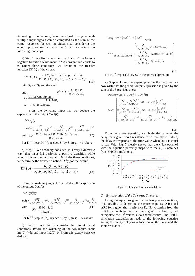
delay for a given short resistance for a zero skew. Indeed, the delay corresponds to the time value when Out1 is equal to half Vdd. Fig. 7 clearly shows that the d(Rs) obtained with the equation perfectly maps with the d(Rs) obtained from SPICE simulations.
Figure 7. Computed and simulated d(Rs)
C. Extrapolation of the Tdf versus Tsk curves
Using the equations given in the two previous sections, it is possible to determine the extreme points D(Rs) and d(Rs) for a given short resistance Rs. Now, starting from the SPICE simulations as the ones given in Fig. 5, we extrapolate the Tdf versus skew characteristics. The SPICE simulation extrapolation leads to the following equation giving the faulty delay as a function of the skew and the short resistance:
)()()(
)(2121
1111
SpSpCRRR
RRpCCRRpTF
eqS
SCS
−⋅−⋅⋅⋅⋅++⋅+⋅⋅=
CCeq CCCCCCC ⋅+⋅+⋅= 2211
( ) ( ) ( )eqS
SCSC
CRRR
RRCCRRCCRRCCb
⋅⋅⋅⋅⋅++⋅⋅++⋅⋅+=
21
22212111
CCeq CCCCCCC ⋅+⋅+⋅= 2211
( ) ( ) ( )eqS
SCSC
CRRR
RRCCRRCCRRCCb
⋅⋅⋅⋅⋅++⋅⋅++⋅⋅+=
21
22212111
)()(
2
22 τ
τ+⋅
=pp
pIn
S
ttSS
tSS
RRR
Re
SS
Ke
SSSS
Ke
SSSS
KtOut
+++
+⋅+−
+⋅−⋅⋅
++⋅−⋅
⋅−= ⋅−
−⋅⋅
21
12
2122
222
22122
2221
21121
1222
1 )()()()()()()( τ
τ
ττττ
ττ
)()()()( 31
21
111 tOuttOuttOuttOut ++=
+++
+⋅+−
+⋅+
−⋅
⋅−+
+⋅+⋅
++
+
−⋅
⋅−+
+⋅+⋅
++
−
=
⋅−−
⋅−−
⋅
⋅
S
tt
tSS
SS
tSS
SS
RRR
Re
SS
Ke
SS
K
SS
eKSS
SS
K
S
K
SS
eKSS
SS
K
S
K
tOut
21
12
2122
221
1112
11
12
22
312222
222
12
21
12
11
312211
122
11
11
1
)()()()(
)()(
)(
)()(
)(
)(
ττ
ττ
ττττ
ττ
τ
ττ
τ
tSStSS eKeKtOut ⋅⋅ ⋅−⋅= 112233
31 )(
[ ]
⋅⋅⋅⋅++
+−
⋅++⋅⋅++
+−
⋅−⋅⋅++
−
−⋅⋅⋅=
1221
2
12121
2
2221
2
2123 )(
)(
)(
11
SCRRRRR
RR
CRCCRRRR
RR
CRCRRRR
R
SSCRRK
eqSS
S
CSS
S
CSS
eqS
S
11
1)(
τ+=
ppIn
ttSS
tSS
eSS
Ke
SSS
Ke
SSS
KtOut ⋅−
−⋅⋅
+⋅++
−⋅+−
−⋅+= 1
1112
111
1211
112
1212
211
1 )()()()()()()( τ
τ
ττττ
eqS
S
CRRR
RRRpbp
⋅⋅⋅+++⋅+
21
212
)()()1(
)(2121
22
SpSpCRRR
pCRRpTF
eqS
CS
−⋅−⋅⋅⋅⋅⋅⋅+⋅=
eqS
SSCSS
CRRR
RRSCRRSCRRK
⋅⋅⋅++⋅⋅⋅+⋅⋅⋅=
21
1111111
1
eqS
CSS
CRR
SCRK
⋅⋅+⋅⋅=
1
12
11

(17) As a validation of the proposed model, we compare in
Fig. 8, for different resistance values, the simulated delay characteristics and the computed ones (equation 12). The agreement is good and so, we can easily extract from these characteristics the maximum resistance Rs
max(f i) corresponding to a delay equal to the slack time. Indeed, as already explained in Fig. 5, using Tsk(f i) and Tsl(f i) as inputs, the intersection gives the maximum detectable short resistance Rs
max(f i).
Figure 8. Computed vs. simulated Tdf vs Tsk characteristics
TABLE I. COMPUTED AND SIMULATED EFFICIENCY FUNCTIONS
Remember that the ultimate goal of the model is to allow
fast computation of the efficiency function εfi(tpj) (equation 7) during fault size based fault simulation. Indeed, during simulation, the maximum resistance allows to compute the detection probability of the resistive short both for the considered test pair and for the best test pair. An efficiency function close to 1 means that the used test pair is as efficient as the best possible test pair. In table 1, the efficiency function is computed using equation (12) for 3 different gates, i.e. for different equivalent R1 and R2, each
gate for two coupling capacitances (40fF and 70 fF), each gate for two different skews (1ns and 0.5ns). The computed function is compared to the value obtained with accurate but time consuming SPICE simulations. We observe that the agreement is very good for the different values of the efficiency functions.
V. CONCLUSION
In this paper, we propose an electrical model to efficiently compute the maximum detected resistance in case of crosstalk aggravated resistive shorts. The electrical model is used during fault size based fault simulation to avoid prohibitive CPU time consuming electrical simulations. Agreement between computed and SPICE simulated efficiency functions proves the validity of the model.
REFERENCES [1] [1] Y. Sato, S. Hamada, T. Maeda, A. Takatori and S. Kajihara,
“Evaluation of the statistical delay quality model”, In ASP Design Autom. Conf., pp. 305-310, 2005.
[2] [2] R. Rodriguez-Montañés, J.P. de Gyvez and P. Volf, “Resistance Characterization for Weak Open Defects”, IEEE Design and Test of Computers, 19(5):18-26, 2002.
[3] [3] W. Needham, C. Prunty, E. Hong Yeoh, “High Volume Processor Test Escape, an Analysis of Defect our Test are Missing”, International Test Conference, pp. 25-34, 1998.
[4] [4] Z. Li, X. Lu, W.Qiu, W. Shi, D. Walker, “A circuit level fault model for resistive opens and bridges”, Trans. On Design Automation of Elect. System, vol. 8, n°4, pp 546-559, 2003.
[5] [5] D. Arumi, R. Rodriguez-Montañés and J. Figueras, “Defective behaviours of resistive opens in interconnect lines”, Proc. of European Test Symp., pp. 28-33, 2005.
[6] [6] J.C.-M. Li, C.-W. Tseng and E.J. McCluskey, “Testing for Resistive Opens and Stuck-opens”, International Test Conference, pp. 1049-1058, 2001.
[7] [7] H. Konuk, “Fault Simulation of Interconnect Opens in Digital CMOS Circuits”, Intern. Conf. on CAD, pp. 548-554, 1997.
[8] [8] Y. Sato, I. Yamazaki, H. Yamanaka, T. Ikeda and M. Takakura, “A Persistant Diagnostic Technique for unstable defects”, International Test Conference, pp. 242-249, 2002.
[9] [9] S. Spinner, J. Jiang, I. Polian, P. Engelke and B. Becker, “Simulating Open-Via defects”, Asian Test Symp., pp. 265-270, 2007.
[10] [10] A.K. Pramanick and S.M. Reddy, “On the Fault Detection Coverage of Gate Delay Fault detecting tests”, IEEE Trans. On CAD, 16(1): 78-94, 1997.
[11] [11] S. Irajpour, S.K. Gupta and M.A. Breuer, “Multiple Tests for each gate delay fault: Higher coverage and lower test application cost”, International Test Conference, 2005.
[12] [12] M. Renovell, P. Huc and Y. Bertrand, “The Concept of Resistance Interval: A New Parametric Model for Resistive Bridging Fault”, VLSI Test Symp., pp. 184-189, 1995.
[13] [13] A. Czutro, N. Houarche, P. Engelke, I. Polian, M. Comte, M. Renovell and B. Becker, “ A Simulator of Small-Delay Faults Caused by Resistive-Open Defects”, European Test Symp., pp. 265-270, 2008.
[14] [14] L. Wang, S. Gupta, M. Breuer, “Modeling and simulation for crosstalk aggravated by weak-bridge defects between on-chip interconnects”, Proc. Asian Test Symposium, pp. 440-447, 2004.
[15] [15] R. Montañés, E. Bruls, J. Figueras, “Bridging defects resistance measurements in a CMOS process”, Proc. International Test Conference, pp. 892-899, 1992.
)(99.0
)()(1),( )99.01ln(
10 9
SiSiSi
T
skSf
d RdRdRD
eTRT
sk
+−⋅
−= −− −
Simul Comput
R1=2600Ω R2=2400Ω Cc=40fF
R1=2600Ω R2=2400Ω Cc=70fF
0.88 0.82
0.88 0.82
Tsk = 1ns Tsl = 500ps Simul Comput
R1=2600Ω R2=2400Ω Cc=40fF
R1=2600Ω R2=2400Ω Cc=70fF
0.85 0.75
0.85 0.75
Tsk = 0.5ns Tsl = 500ps
b) Gate 2
Simul Comput
R1=1950Ω R2=1900Ω Cc=40fF
R1=1950Ω R2=1900Ω Cc=70fF
0.47 0.44
0.47 0.44
Tsk = 1ns Tsl = 500ps Simul Comput
R1=1950Ω R2=1900Ω Cc=40fF
R1=1950Ω R2=1900Ω Cc=70fF
0.46 0.39
0.46 0.39
Tsk = 0.5ns Tsl = 500ps
a) Gate 1
Simul Comput
R1=2900Ω R2=2600Ω Cc=40fF
R1=2900Ω R2=2600Ω Cc=70fF
1.00 0.99
1.00 0.99
Tsk = 1ns Tsl = 500ps Simul Comput
R1=2900Ω R2=2600Ω Cc=40fF
R1=2900Ω R2=2600Ω Cc=70fF
1.00 0.99
1.00 0.99
Tsk = 0.5ns Tsl = 500ps
c) Gate 3
Simul Comput
R1=2600Ω R2=2400Ω Cc=40fF
R1=2600Ω R2=2400Ω Cc=70fF
0.88 0.82
0.88 0.82
Tsk = 1ns Tsl = 500ps Simul Comput
R1=2600Ω R2=2400Ω Cc=40fF
R1=2600Ω R2=2400Ω Cc=70fF
0.85 0.75
0.85 0.75
Tsk = 0.5ns Tsl = 500ps
b) Gate 2
Simul Comput
R1=2600Ω R2=2400Ω Cc=40fF
R1=2600Ω R2=2400Ω Cc=70fF
0.88 0.82
0.88 0.82
Tsk = 1ns Tsl = 500ps Simul Comput
R1=2600Ω R2=2400Ω Cc=40fF
R1=2600Ω R2=2400Ω Cc=70fF
0.88 0.820.88 0.82
0.88 0.820.88 0.82
Tsk = 1ns Tsl = 500psTsk = 1ns Tsl = 500ps Simul Comput
R1=2600Ω R2=2400Ω Cc=40fF
R1=2600Ω R2=2400Ω Cc=70fF
0.85 0.75
0.85 0.75
Tsk = 0.5ns Tsl = 500ps Simul Comput
R1=2600Ω R2=2400Ω Cc=40fF
R1=2600Ω R2=2400Ω Cc=70fF
0.85 0.750.85 0.75
0.85 0.750.85 0.75
Tsk = 0.5ns Tsl = 500psTsk = 0.5ns Tsl = 500ps
b) Gate 2
Simul Comput
R1=1950Ω R2=1900Ω Cc=40fF
R1=1950Ω R2=1900Ω Cc=70fF
0.47 0.44
0.47 0.44
Tsk = 1ns Tsl = 500ps Simul Comput
R1=1950Ω R2=1900Ω Cc=40fF
R1=1950Ω R2=1900Ω Cc=70fF
0.46 0.39
0.46 0.39
Tsk = 0.5ns Tsl = 500ps
a) Gate 1
Simul Comput
R1=1950Ω R2=1900Ω Cc=40fF
R1=1950Ω R2=1900Ω Cc=70fF
0.47 0.44
0.47 0.44
Tsk = 1ns Tsl = 500ps Simul Comput
R1=1950Ω R2=1900Ω Cc=40fF
R1=1950Ω R2=1900Ω Cc=70fF
0.47 0.440.47 0.44
0.47 0.440.47 0.44
Tsk = 1ns Tsl = 500psTsk = 1ns Tsl = 500ps Simul Comput
R1=1950Ω R2=1900Ω Cc=40fF
R1=1950Ω R2=1900Ω Cc=70fF
0.46 0.39
0.46 0.39
Tsk = 0.5ns Tsl = 500ps Simul Comput
R1=1950Ω R2=1900Ω Cc=40fF
R1=1950Ω R2=1900Ω Cc=70fF
0.46 0.390.46 0.39
0.46 0.390.46 0.39
Tsk = 0.5ns Tsl = 500psTsk = 0.5ns Tsl = 500ps
a) Gate 1
Simul Comput
R1=2900Ω R2=2600Ω Cc=40fF
R1=2900Ω R2=2600Ω Cc=70fF
1.00 0.99
1.00 0.99
Tsk = 1ns Tsl = 500ps Simul Comput
R1=2900Ω R2=2600Ω Cc=40fF
R1=2900Ω R2=2600Ω Cc=70fF
1.00 0.99
1.00 0.99
Tsk = 0.5ns Tsl = 500ps
c) Gate 3
Simul Comput
R1=2900Ω R2=2600Ω Cc=40fF
R1=2900Ω R2=2600Ω Cc=70fF
1.00 0.99
1.00 0.99
Tsk = 1ns Tsl = 500ps Simul Comput
R1=2900Ω R2=2600Ω Cc=40fF
R1=2900Ω R2=2600Ω Cc=70fF
1.00 0.991.00 0.99
1.00 0.991.00 0.99
Tsk = 1ns Tsl = 500psTsk = 1ns Tsl = 500ps Simul Comput
R1=2900Ω R2=2600Ω Cc=40fF
R1=2900Ω R2=2600Ω Cc=70fF
1.00 0.99
1.00 0.99
Tsk = 0.5ns Tsl = 500ps Simul Comput
R1=2900Ω R2=2600Ω Cc=40fF
R1=2900Ω R2=2600Ω Cc=70fF
1.00 0.991.00 0.99
1.00 0.991.00 0.99
Tsk = 0.5ns Tsl = 500psTsk = 0.5ns Tsl = 500ps
c) Gate 3