An Efficient Hybrid Parallel Prefix Adders for Reverse Converters using QCA Technology€¦ · ·...
6
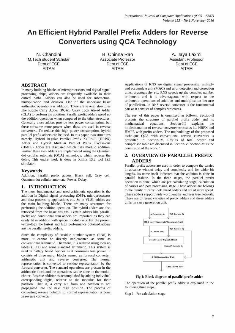
International Journal of Computer Applications (0975 – 8887) Volume 153 – No.1,November 2016 7 An Efficient Hybrid Parallel Prefix Adders for Reverse Converters using QCA Technology N. Chandini M.Tech student Scholar Dept.of ECE AITAM B. Chinna Rao Associate Professor Dept.of ECE AITAM A. Jaya Laxmi Assistant Professor Dept.of ECE AITAM ABSTRACT In many building blocks of microprocessors and digital signal processing chips, adders are frequently available in their critical paths. Adders can also be used for subtraction, multiplication and division. One of the important basic arithmetic operations is addition. There are several structures like Ripple Carry Adder (RCA), Carry Look Ahead Adder (CLA) to perform the addition. Parallel prefix adders speed up the addition operation when compared to the other structures. Generally these adders provide less power consumption, but these consume more power when these are used in reverse converters. To reduce this high power consumption, hybrid parallel prefix adders can be used. In this paper, two structures namely, Hybrid Regular Parallel Prefix XOR/OR (HRPX) Adder and Hybrid Modular Parallel Prefix Excess-one (HMPE) Adder are discussed which uses modulo addition. Further these two adders are implemented using the Quantum dot cellular automata (QCA) technology, which reduces the delay. This entire work is done in Xilinx 13.2 tool ISE simulator. Keywords Addition, Parallel prefix adders, Black cell, Gray cell, Quantum dot cellular automata, Power, Delay. 1. INTRODUCTION The most fundamental and used arithmetic operation is the addition in Digital signal processing (DSP), microprocessors and data processing applications etc. So in VLSI, adders are the main building blocks. There are many structures for performing the addition operation. The hybrid adders are also retrieved from the basic designs. Certain adders like parallel prefix and conditional sum adders are important as they can easily fit in addition with special modulo sets. For the present technology the fastest and high performance obtained adders are the parallel prefix adders. Since the complexity of Residue number system (RNS) is more, it cannot be directly implemented as same as conventional arithmetic. Therefore, it is realized using look up tables (LUT) and some standard arithmetic. This system is used in battery based devices as it consumes less power. It consists of three major blocks named as forward converter, arithmetic unit and reverse converter. The normal representation is converted to residue representation by the forward converter. The standard operations are present in the arithmetic block and the operations can be done on the moduli choice. Residue addition is accomplished by adding individual corresponding digits, relative to the modulus for their position. That is, a carry out from one position is not propagated into the next digit position. The process of converting reverse notation to normal representation is done in reverse converter. Applications of RNS are digital signal processing, multiply and accumulate unit (MAC) and error detection and correction units, cryptography etc. RNS speeds up the complex number arithmetic and it is advantageous with respect to the arithmetic operations of addition and multiplication because of parallelism. In RNS reverse converter is the fundamental part as it consists of complex structures. The rest of this paper is organized as follows. Section-II presents the structure of parallel prefix adder and its mathematical equations. Section-III explains the implementation of reverse converter structures i.e. HRPX and HMPE with prefix adders. The methodology of the proposed technique QCA with conventional reverse converters is presented in Section-IV. Results of total power and comparison table are discussed in Section-V. Section-VI is the conclusion of the work. „ 2. OVERVIEW OF PARALLEL PREFIX ADDERS Parallel prefix adders are used in order to compute the carries in advance without delay and complexity and for wider bit lengths. Its name itself indicates that the addition is done in parallel fashion. In the three stages, the parallel prefix operation is done, which are pre calculating stage, calculation of carries and post processing stage. These adders are belongs to the family of carry look ahead adders and are of more speed. These adders support wide word lengths and uses tree network. There are different varieties of prefix adders and these adders differ in carry generation unit. Fig 1: Block diagram of parallel prefix adder The operation of the parallel prefix adder is explained in the following three steps. Step 1: Pre calculation stage
Transcript of An Efficient Hybrid Parallel Prefix Adders for Reverse Converters using QCA Technology€¦ · ·...
International Journal of Computer Applications (0975 – 8887)
Volume 153 – No.1,November 2016
7
An Efficient Hybrid Parallel Prefix Adders for Reverse
Converters using QCA Technology
N. Chandini M.Tech student Scholar
Dept.of ECE AITAM
B. Chinna Rao Associate Professor
Dept.of ECE AITAM
A. Jaya Laxmi Assistant Professor
Dept.of ECE AITAM
ABSTRACT In many building blocks of microprocessors and digital signal
processing chips, adders are frequently available in their
critical paths. Adders can also be used for subtraction,
multiplication and division. One of the important basic
arithmetic operations is addition. There are several structures
like Ripple Carry Adder (RCA), Carry Look Ahead Adder
(CLA) to perform the addition. Parallel prefix adders speed up
the addition operation when compared to the other structures.
Generally these adders provide less power consumption, but
these consume more power when these are used in reverse
converters. To reduce this high power consumption, hybrid
parallel prefix adders can be used. In this paper, two structures
namely, Hybrid Regular Parallel Prefix XOR/OR (HRPX)
Adder and Hybrid Modular Parallel Prefix Excess-one
(HMPE) Adder are discussed which uses modulo addition.
Further these two adders are implemented using the Quantum
dot cellular automata (QCA) technology, which reduces the
delay. This entire work is done in Xilinx 13.2 tool ISE
simulator.
Keywords Addition, Parallel prefix adders, Black cell, Gray cell,
Quantum dot cellular automata, Power, Delay.
1. INTRODUCTION The most fundamental and used arithmetic operation is the
addition in Digital signal processing (DSP), microprocessors
and data processing applications etc. So in VLSI, adders are
the main building blocks. There are many structures for
performing the addition operation. The hybrid adders are also
retrieved from the basic designs. Certain adders like parallel
prefix and conditional sum adders are important as they can
easily fit in addition with special modulo sets. For the present
technology the fastest and high performance obtained adders
are the parallel prefix adders.
Since the complexity of Residue number system (RNS) is
more, it cannot be directly implemented as same as
conventional arithmetic. Therefore, it is realized using look up
tables (LUT) and some standard arithmetic. This system is
used in battery based devices as it consumes less power. It
consists of three major blocks named as forward converter,
arithmetic unit and reverse converter. The normal
representation is converted to residue representation by the
forward converter. The standard operations are present in the
arithmetic block and the operations can be done on the moduli
choice. Residue addition is accomplished by adding individual
corresponding digits, relative to the modulus for their
position. That is, a carry out from one position is not
propagated into the next digit position. The process of
converting reverse notation to normal representation is done
in reverse converter.
Applications of RNS are digital signal processing, multiply
and accumulate unit (MAC) and error detection and correction
units, cryptography etc. RNS speeds up the complex number
arithmetic and it is advantageous with respect to the
arithmetic operations of addition and multiplication because
of parallelism. In RNS reverse converter is the fundamental
part as it consists of complex structures.
The rest of this paper is organized as follows. Section-II
presents the structure of parallel prefix adder and its
mathematical equations. Section-III explains the
implementation of reverse converter structures i.e. HRPX and
HMPE with prefix adders. The methodology of the proposed
technique QCA with conventional reverse converters is
presented in Section-IV. Results of total power and
comparison table are discussed in Section-V. Section-VI is the
conclusion of the work. „
2. OVERVIEW OF PARALLEL PREFIX
ADDERS Parallel prefix adders are used in order to compute the carries
in advance without delay and complexity and for wider bit
lengths. Its name itself indicates that the addition is done in
parallel fashion. In the three stages, the parallel prefix
operation is done, which are pre calculating stage, calculation
of carries and post processing stage. These adders are belongs
to the family of carry look ahead adders and are of more speed.
These adders support wide word lengths and uses tree network.
There are different varieties of prefix adders and these adders
differ in carry generation unit.
Fig 1: Block diagram of parallel prefix adder
The operation of the parallel prefix adder is explained in the
following three steps.
Step 1: Pre calculation stage
International Journal of Computer Applications (0975 – 8887)
Volume 153 – No.1,November 2016
8
In this stage, the inputs are given and then propagate and
generate unit calculates the carry generate and propagate based
on the below formulae.
Pi = AixorBi
Gi = AiandBi
Step 2: Prefix calculation stage
Carry signals are generated by using different prefix graphs.
These calculated values are forwarded to summation stage
after calculation of these carry prefixes. The group
generate/propagate signals are computed by using the below
equations. The black cells and gray cells are included in this
stage for easy computation of carry prefixes. The black cell
(BC) generates ordered pair and the gray cells (GC) generate
only left signals.
P = Pi and Pi prev
G = Pi and Gi prev or Gi
Fig 2: Representation of Black cells and gray cells
The operation is done in parallel fashion by decomposing into
smaller pieces. The combined operator used in this stage
consists of two AND gates and the OR gate. Each vertical
stage gives out the respective propagate and generate values.
Fig 3: Block diagram of combined operator P & G
Step 3: Summation stage
The calculated values of carries are forwarded to the post
processing stage. The final sum values are calculated in this
stage. A dot operator (.) is used in the simplification of
generate and propagate terms.
𝑆𝑖 = 𝑃𝑖𝑥𝑜𝑟𝐶𝑖−1
𝐶𝑖 = 𝐺𝑖 Out of these three steps, 1 and 3 steps are fast as they involved
with simple operations to each bit position. The step2 involves
propagation of carries and the whole performance depends on
this step. There are different kinds of prefix structures. They
are:
J.Sklansky – conditional adder.
Ladner- Fisher adder.
Kogge- Stone adder.
Brent- Kung adder.
Han Carlson adder.
Out of these adders, KS and BK adders are used in this work
and are discussed below.
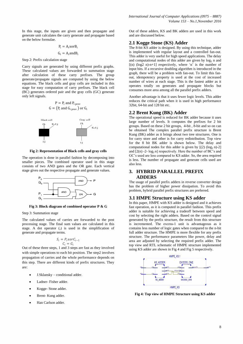
2.1 Kogge Stone (KS) Adder The 8-bit KS adder is designed. By using this technique, adder
is implemented with regular layout and a controlled fan-out.
This adder is very useful for high speed applications. The delay
and computational nodes of this adder are given by log2 n and
[(n) (log2 n)-n+1] respectively, where „n‟ is the number of
input bits. If a recursive doubling algorithm is introduced in the
graph, there will be a problem with fan-out. To limit this fan-
out, idempotency property is used at the cost of increased
number of wires at each stage. This is the fastest adder as it
operates totally on generates and propagate blocks but
consumes more area among all the parallel prefix adders.
Another advantage is that it uses fewer logic levels. This adder
reduces the critical path when it is used in high performance
32bit, 64-bit and 128 bit etc.
2.2 Brent Kung (BK) Adder The operational speed is reduced for BK adder because it uses
large number of levels. It computes the prefixes for 2 bit
groups. Based on these 2 bit groups, 4-bit , 8-bit and so on can
be obtained The complex parallel prefix structure is Brent
Kung (BK) adder as it brings about two tree structures. One is
for carry store and other is for carry redistribution. Top view
for the 8 bit BK adder is shown below. The delay and
computational nodes for this adder is given by [(2) (log2 n)-2]
and [2(n) -2- log2 n] respectively. Here the number of BC‟s and
GC‟s used are less compared to KS adder. So, the area required
is less. The number of propagate and generate cells used are
also less.
3. HYBRID PARALLEL PREFIX
ADDERS The usage of parallel prefix adders in reverse converter design
has the problem of higher power dissipation. To avoid this
problem, hybrid parallel prefix structures are preferred.
3.1 HMPE Structure using KS adder In this paper, HMPE with KS adder is designed and it achieves
fast operation, as it is computed in parallel fashion. This prefix
adder is suitable for achieving a tradeoff between speed and
cost by selecting the right adders. Based on the control signal
generated by the prefix structure, the result from this structure
is incremented. The excess-1 unit is advantageous as it
contains less number of logic gates when compared to the n-bit
full adder structure. The HMPE is more flexible for any prefix
structure. The performance parameters like power, delay and
area are adjusted by selecting the required prefix adder. The
top view and RTL schematic of HMPE structure implemented
using KS adder are shown in Fig 4 and Fig 5 respectively.
Fig 4: Top view of HMPE Structure using KS adder
International Journal of Computer Applications (0975 – 8887)
Volume 153 – No.1,November 2016
9
Fig 5: RTL schematic of HMPE Structure using KS adder
Generally, the carry-in depends on the carry-out in End
Around Carry (EAC) adder. This means that the output carry is
feedback to carry in through some logic, which is used in
modulo additions. Both carry in and carry out generation
processing conditions have to be met to obtain fast end around
carry. With fast processing, the parallel prefix adder fulfills all
these requirements. For modulo addition,
A + B = A + B + 1 if A + B ≥ 2n
A + B otherwise
The carry out obtained from this addition determines whether
the carry out is normal or incremented carry out is added to
sum. This results in double zero representation. For single zero
representation, the condition 𝐴 + 𝐵 ≥ 2𝑛 − 1 is fulfilled if
either 𝐴 + 𝐵 ≥ 2𝑛 or 𝐴 + 𝐵 = 2𝑛 − 1 which corresponds to
propagate signal of prefix adder. By using prefix adder,
modulo addition with single zero representation can be easily
implemented.
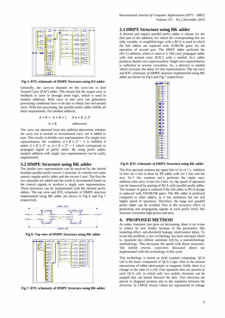
3.2 HMPE Structure using BK adder The double zero representation can be resolved by the hybrid
modular parallel prefix excess-1 structure. It contains two units
namely regular prefix adder and the excess-1 unit. The first the
two operands are added and the result is incremented based on
the control signals to produce a single zero representation.
These structures can be implemented with the desired prefix
adders. The top view and RTL schematic of HMPE structure
implemented using BK adder are shown in Fig 6 and Fig 7
respectively.
Fig 6: Top view of HMPE Structure using BK adder
Fig 7: RTL schematic of HMPE Structure using BK adder
3.3 HRPX Structure using BK adder A desired and regular parallel prefix adder is chosen for the
first part of the addition, for which the corresponding bits are
fully variable. A simplified logic with a RCA is used in which
the full adders are replaced with XOR/OR gates for the
operation of second part. The HRPX adder performs the
(4n+1) addition, where n value is 4. The carry propagate adder
with end around carry (EAC) with a moduli 2n-1 adder
produces double zero representation. Single zero representation
is sufficient in reverse converters. So, a detector is needed
which increases the delay for this representation. The top view
and RTL schematic of HMPE structure implemented using BK
adder are shown in Fig 6 and Fig 7 respectively.
Fig 8: RTL schematic of HRPX Structure using BK adder
The first operand contains the upper bits of 2n of 1‟s. Addition
of first 2n+1 bits is done by PP adder with 2n+1 bits and the
next 2n+1 bits contains one‟s performs the ripple carry
addition with carry of last 2n+1 bits. So, the speed of operation
can be improved by pairing of RCA with parallel prefix adder.
The number of gates is reduced if the full adder in RCA design
is replaced with XNOR/OR gates. The BK adder is preferred
compared to other adders, as it has minimum fan out and
higher speed of operation. Therefore, the large size parallel
prefix adder can be avoided. Due to the recursive effect of
generating and propagating signals at each prefix level, this
structure consumes high power and area.
4. PROPOSED METHOD As today transistor size goes on decreasing, there is no scope
to reduce its size further because of the parameters like
tunneling effect, sub-threshold leakage, interconnect delay. To
avoid this problem, a new technology has been emerged which
is, Quantum dot cellular automata (QCA), a nanotechnology
methodology. This decreases the speed with dense structures.
The hybrid reverse converters discussed above are
implemented with this technology in this work.
This technology is based on field coupled computing. QCA
cell is the basic component of QCA Logic. Due to the mutual
interactions of either electrostatic or magnetic fields, there is a
change in the state of a cell. Four quantum dots are present in
each QCA cell, in which only two mobile electrons can be
trapped that can tunnel between the dots. Two electrons are
placed in diagonal position due to the repulsion between the
electrons. In CMOS, binary values are represented in voltage
International Journal of Computer Applications (0975 – 8887)
Volume 153 – No.1,November 2016
10
or current levels. Just like that, electron position represents the
binary values in this technology. The two basic logic devices
of QCA are Majority gate and Inverter.
4.1 Implementation of Hybrid Structures
using QCA technology Using QCA technology, any parallel prefix adder can be
implemented. Majority gate contains 5 QCA cells. Out of these
five cells, 3 are input cells, one intermediate cell and one
output cell. The operation of this majority gate is described by
below equation.
Fig 9: Representation of majority gate
Fig 10: Schematic of Majority gate.
M a, b, c = a. b + a. c + b. c
The majority gate output is calculated by using the above
formula. There will be 8 combinations for three inputs. The
above structures HRPX BK, HMPE BK and HMPE KS are
implemented by using QCA technology. The entire operation
is same as before. The only that make difference is the prefix
adders are implemented using majority gates rather than
CMOS logic gates. The implementation of BK and KS prefix
adders with majority gates are shown in Fig.11 and Fig.12
respectively.
Fig 11: Brent Kung adder with majority gates
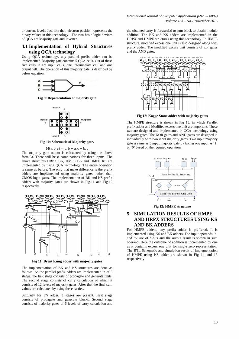
The implementation of BK and KS structures are done as
follows. As the parallel prefix adders are implemented in of 3
stages, the first stage consists of propagate and generate units.
The second stage consists of carry calculation of which it
consists of 12 levels of majority gates. After that the final sum
values are calculated by using these carries.
Similarly for KS adder, 3 stages are present. First stage
consists of propagate and generate blocks. Second stage
consists of majority gates of 6 levels of carry calculation and
the obtained carry is forwarded to sum block to obtain modulo
addition. The BK and KS adders are implemented in the
HRPX and HMPE structures using this technology. In HMPE
structure, modified excess one unit is also designed along with
prefix adder. The modified excess unit consists of xor gates
and the AND gates.
Fig 12: Kogge Stone adder with majority gates
The HMPE structure is shown in Fig 13, in which Parallel
prefix adder and Modified excess one unit are important. These
two are designed and implemented in QCA technology using
majority gates. The XOR gates and AND gates are designed in
individually with two input majority gates. Two input majority
gate is same as 3 input majority gate by taking one input as „1‟
or „0‟ based on the required operation.
Fig 13: HMPE structure
5. SIMULATION RESULTS OF HMPE
AND HRPX STRUCTURES USING KS
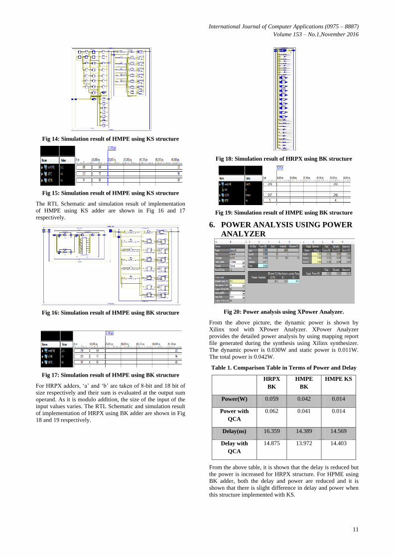
AND BK ADDERS For HMPE adders, any prefix adder is preffered. It is
implemented using KS and BK adders. The input operands „a‟
and „b‟ are of 8-bits and the output result is shown in sum
operand. Here the outcome of addition is incremented by one
as it contains excess one unit for single zero representation.
The RTL Schematic and simulation result of implementation
of HMPE using KS adder are shown in Fig 14 and 15
respectively.
International Journal of Computer Applications (0975 – 8887)
Volume 153 – No.1,November 2016
11
Fig 14: Simulation result of HMPE using KS structure
Fig 15: Simulation result of HMPE using KS structure
The RTL Schematic and simulation result of implementation
of HMPE using KS adder are shown in Fig 16 and 17
respectively.
Fig 16: Simulation result of HMPE using BK structure
Fig 17: Simulation result of HMPE using BK structure
For HRPX adders, „a‟ and „b‟ are taken of 8-bit and 18 bit of
size respectively and their sum is evaluated at the output sum
operand. As it is modulo addition, the size of the input of the
input values varies. The RTL Schematic and simulation result
of implementation of HRPX using BK adder are shown in Fig
18 and 19 respectively.
Fig 18: Simulation result of HRPX using BK structure
Fig 19: Simulation result of HMPE using BK structure
6. POWER ANALYSIS USING POWER
ANALYZER
Fig 20: Power analysis using XPower Analyzer.
From the above picture, the dynamic power is shown by
Xilinx tool with XPower Analyzer. XPower Analyzer
provides the detailed power analysis by using mapping report
file generated during the synthesis using Xilinx synthesizer.
The dynamic power is 0.030W and static power is 0.011W.
The total power is 0.042W.
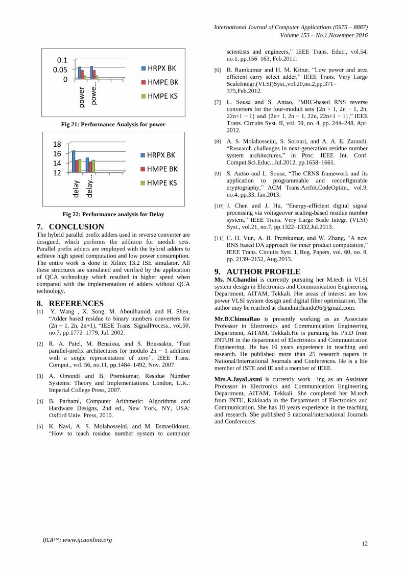
Table 1. Comparison Table in Terms of Power and Delay
HRPX
BK
HMPE
BK
HMPE KS
Power(W) 0.059 0.042 0.014
Power with
QCA
0.062 0.041 0.014
Delay(ns) 16.359 14.389 14.569
Delay with
QCA
14.875 13.972 14.403
From the above table, it is shown that the delay is reduced but
the power is increased for HRPX structure. For HPME using
BK adder, both the delay and power are reduced and it is
shown that there is slight difference in delay and power when
this structure implemented with KS.
International Journal of Computer Applications (0975 – 8887)
Volume 153 – No.1,November 2016
12
Fig 21: Performance Analysis for power
Fig 22: Performance analysis for Delay
7. CONCLUSION The hybrid parallel prefix adders used in reverse converter are
designed, which performs the addition for moduli sets.
Parallel prefix adders are employed with the hybrid adders to
achieve high speed computation and low power consumption.
The entire work is done in Xilinx 13.2 ISE simulator. All
these structures are simulated and verified by the application
of QCA technology which resulted in higher speed when
compared with the implementation of adders without QCA
technology.
8. REFERENCES [1] Y. Wang , X. Song, M. Aboulhamid, and H. Shen,
“Adder based residue to binary numbers converters for
(2n − 1, 2n, 2n+1), “IEEE Trans. SignalProcess., vol.50,
no.7, pp.1772–1779, Jul. 2002.
[2] R. A. Patel, M. Benaissa, and S. Boussakta, “Fast
parallel-prefix architectures for modulo 2n − 1 addition
with a single representation of zero”, IEEE Trans.
Comput., vol. 56, no.11, pp.1484–1492, Nov. 2007.
[3] A. Omondi and B. Premkumar, Residue Number
Systems: Theory and Implementations. London, U.K.:
Imperial College Press, 2007.
[4] B. Parhami, Computer Arithmetic: Algorithms and
Hardware Designs, 2nd ed., New York, NY, USA:
Oxford Univ. Press, 2010.
[5] K. Navi, A. S. Molahosseini, and M. Esmaeildoust,
“How to teach residue number system to computer
scientists and engineers,” IEEE Trans. Educ., vol.54,
no.1, pp.156–163, Feb.2011.
[6] B. Ramkumar and H. M. Kittur, “Low power and area
efficient carry select adder,” IEEE Trans. Very Large
ScaleIntegr.(VLSI)Syst.,vol.20,no.2,pp.371–
375,Feb.2012.
[7] L. Sousa and S. Antao, “MRC-based RNS reverse
converters for the four-moduli sets {2n + 1, 2n − 1, 2n,
22n+1 − 1} and {2n+ 1, 2n − 1, 22n, 22n+1 − 1},” IEEE
Trans. Circuits Syst. II, vol. 59, no. 4, pp. 244–248, Apr.
2012.
[8] A. S. Molahosseini, S. Sorouri, and A. A. E. Zarandi,
“Research challenges in next-generation residue number
system architectures,” in Proc. IEEE Int. Conf.
Comput.Sci.Educ., Jul.2012, pp.1658–1661.
[9] S. Antão and L. Sousa, “The CRNS framework and its
application to programmable and reconfigurable
cryptography,” ACM Trans.Archit.CodeOptim., vol.9,
no.4, pp.33, Jan.2013.
[10] J. Chen and J. Hu, “Energy-efficient digital signal
processing via voltageover scaling-based residue number
system,” IEEE Trans. Very Large Scale Integr. (VLSI)
Syst., vol.21, no.7, pp.1322–1332,Jul.2013.
[11] C. H. Vun, A. B. Premkumar, and W. Zhang, “A new
RNS based DA approach for inner product computation,”
IEEE Trans. Circuits Syst. I, Reg. Papers, vol. 60, no. 8,
pp. 2139–2152, Aug.2013.
9. AUTHOR PROFILE Ms. N.Chandini is currently pursuing her M.tech in VLSI
system design in Electronics and Communication Engineering
Department, AITAM, Tekkali. Her areas of interest are low
power VLSI system design and digital filter optimization. The
author may be reached at [email protected].
Mr.B.ChinnaRao is presently working as an Associate
Professor in Electronics and Communication Engineering
Department, AITAM, Tekkali.He is pursuing his Ph.D from
JNTUH in the department of Electronics and Communication
Engineering. He has 16 years experience in teaching and
research. He published more than 25 research papers in
National/International Journals and Conferences. He is a life
member of ISTE and IE and a member of IEEE.
Mrs.A.JayaLaxmi is currently work ing as an Assistant
Professor in Electronics and Communication Engineering
Department, AITAM, Tekkali. She completed her M.tech
from JNTU, Kakinada in the Department of Electronics and
Communication. She has 10 years experience in the teaching
and research. She published 5 national/international Journals
and Conferences.
00.05
0.1
po
wer
po
we…
HRPX BK
HMPE BK
HMPE KS
12141618
del
ay
del
ay …
HRPX BK
HMPE BK
HMPE KS
IJCATM : www.ijcaonline.org