Also Covering Legacy Programmers 2900, 3900 and...
272
3980 Programming System User Manual Also Covering Legacy Programmers 2900, 3900 and 3980 2006 Updated contact information and improved navigation 981-0414-002D xpi
-
Upload
nguyendung -
Category
Documents
-
view
230 -
download
0
Transcript of Also Covering Legacy Programmers 2900, 3900 and...

3980 Programming System User ManualAlso Covering Legacy Programmers 2900, 3900 and 3980
2006 Updated contact information and improved navigation
981-0414-002D
xpi

981-0414-002D
Data I/O has made every attempt to ensure that the information in this document is accurate and complete. Data I/O assumes no liability for errors or for any incidental, consequential, indirect, or special damages, including, without limitation, loss of use, loss or alteration of data, delays, or lost profits or savings, arising from the use of this document or the product which it accompanies.
No part of this document may be reproduced or transmitted in any form or by any means, electronic or mechanical, for any purpose without written permission from Data I/O.
Acknowledgments:
Data I/O is a registered trademark and AutoBaud, Keep Current, MatchBook, SmartPort, and HiTerm Terminal Emulator are trademarks of Data I/O Corporation.
Data I/O Corporation acknowledges the trademarks of other organizations for their respective products or services mentioned in this document.
Portions of the 2900, 3900, 3980 and 3980xpi Programming Systems are protected under U.S. Patent numbers 4,837,653; 4,840,576; 5,176,525; and 5,289,118. Other U.S. and Foreign Patents Pending.
© 2001, 2006 Data I/O Corporation All rights reserved
Data I/O Corporation6464 185th Avenue N.E., Suite 101Redmond, Washington USA 98052(425) 881-6444http://www.dataio.com

3980xpi/3980/3900/2900 User Manual iii
Contents
ContentsFigures . . . . . . . . . . . . . . . . . . . . . . . . . . . . . . . . . . . . . . . . . . . . . . . viii
PrefaceData I/O Customer Support . . . . . . . . . . . . . . . . . . . . . . . . . . . . . . . . . xiContacting Data I/O . . . . . . . . . . . . . . . . . . . . . . . . . . . . . . . . . . . . . . . xiiWarranty Information . . . . . . . . . . . . . . . . . . . . . . . . . . . . . . . . . . . . . . xiiKeep Current Subscription Service . . . . . . . . . . . . . . . . . . . . . . . . . . . . xiiiRepair Service . . . . . . . . . . . . . . . . . . . . . . . . . . . . . . . . . . . . . . . . . . xiiiEnd User Registration and Address Change . . . . . . . . . . . . . . . . . . . . . . xiii
Safety Summary
1. IntroductionProduct Descriptions . . . . . . . . . . . . . . . . . . . . . . . . . . . . . . . . . . . . . . 1-1Configurations . . . . . . . . . . . . . . . . . . . . . . . . . . . . . . . . . . . . . . . . . . 1-1Device Support. . . . . . . . . . . . . . . . . . . . . . . . . . . . . . . . . . . . . . . . . . 1-2Contents of Package . . . . . . . . . . . . . . . . . . . . . . . . . . . . . . . . . . . . . . 1-2External Features . . . . . . . . . . . . . . . . . . . . . . . . . . . . . . . . . . . . . . . . 1-3Disks. . . . . . . . . . . . . . . . . . . . . . . . . . . . . . . . . . . . . . . . . . . . . . . . . 1-4
Programmer Disks . . . . . . . . . . . . . . . . . . . . . . . . . . . . . . . . . . . . . 1-4PC Disk. . . . . . . . . . . . . . . . . . . . . . . . . . . . . . . . . . . . . . . . . . . . . 1-5
Specifications . . . . . . . . . . . . . . . . . . . . . . . . . . . . . . . . . . . . . . . . . . . 1-6Physical and Environmental . . . . . . . . . . . . . . . . . . . . . . . . . . . . . . 1-7Safety . . . . . . . . . . . . . . . . . . . . . . . . . . . . . . . . . . . . . . . . . . . . . 1-7Certificate of RFI/EMI Compliance . . . . . . . . . . . . . . . . . . . . . . . . . . 1-7Performance Verification. . . . . . . . . . . . . . . . . . . . . . . . . . . . . . . . . 1-7
Options . . . . . . . . . . . . . . . . . . . . . . . . . . . . . . . . . . . . . . . . . . . . . . . 1-8
2. Setting Up1. Choose Your Configuration and Connect the Equipment . . . . . . . . . . . . 2-1
Connecting to a PC . . . . . . . . . . . . . . . . . . . . . . . . . . . . . . . . . . . . 2-2Connecting to a Host . . . . . . . . . . . . . . . . . . . . . . . . . . . . . . . . . . . 2-5More About Cables . . . . . . . . . . . . . . . . . . . . . . . . . . . . . . . . . . . . . 2-9
2. Insert Boot Disk in Programmer . . . . . . . . . . . . . . . . . . . . . . . . . . . 2-113. Install the Base. . . . . . . . . . . . . . . . . . . . . . . . . . . . . . . . . . . . . . . 2-124. Turn On the Programmer . . . . . . . . . . . . . . . . . . . . . . . . . . . . . . . 2-155. Check Self-test Results . . . . . . . . . . . . . . . . . . . . . . . . . . . . . . . . . 2-166. Start-up Screen . . . . . . . . . . . . . . . . . . . . . . . . . . . . . . . . . . . . . . 2-187. Set Up High Speed Download (optional) . . . . . . . . . . . . . . . . . . . . . 2-20
Setting Up High Speed Download with TaskLink for Windows/DOS. . . 2-20Setting Up High Speed Serial Download with HiTerm . . . . . . . . . . . . 2-20
8. Install Devices . . . . . . . . . . . . . . . . . . . . . . . . . . . . . . . . . . . . . . . 2-22Inserting a DIP Device into a DIP Base . . . . . . . . . . . . . . . . . . . . . . 2-22Installing a MatchBook into a Base . . . . . . . . . . . . . . . . . . . . . . . . 2-23Inserting a PLCC or LCC Device into a MatchBook . . . . . . . . . . . . . . 2-24

Contents
iv 3980xpi/3980/3900/2900 User Manual
Inserting an SOIC Device into a MatchBook . . . . . . . . . . . . . . . . . . 2-25Inserting a PGA Device into a PGA Base . . . . . . . . . . . . . . . . . . . . . 2-26Installing a PPI Adapter into the PPI Base . . . . . . . . . . . . . . . . . . . 2-27High Profile PPI Adapters . . . . . . . . . . . . . . . . . . . . . . . . . . . . . . . 2-28Inserting Devices in a PPI Adapter . . . . . . . . . . . . . . . . . . . . . . . . . 2-29
9. Preventive Maintenance . . . . . . . . . . . . . . . . . . . . . . . . . . . . . . . . 2-32Cleaning the Fan . . . . . . . . . . . . . . . . . . . . . . . . . . . . . . . . . . . . . 2-32Conductive Pad . . . . . . . . . . . . . . . . . . . . . . . . . . . . . . . . . . . . . . 2-32SPA Block and Base . . . . . . . . . . . . . . . . . . . . . . . . . . . . . . . . . . . 2-33
10. What To Do Next Time. . . . . . . . . . . . . . . . . . . . . . . . . . . . . . . . . 2-3511. Using the Mass Storage Module (MSM) . . . . . . . . . . . . . . . . . . . . . 2-36
3. Getting StartedOutline of the Programming Operation . . . . . . . . . . . . . . . . . . . . . . . . . 3-1Session 1: Programming a Device Using TaskLink. . . . . . . . . . . . . . . . . . 3-2
For TaskLink for Windows . . . . . . . . . . . . . . . . . . . . . . . . . . . . . . . . 3-2Session 2: Navigating Through the Programmer Menus . . . . . . . . . . . . . 3-10
Programmer Main Menu . . . . . . . . . . . . . . . . . . . . . . . . . . . . . . . . 3-10Moving Around . . . . . . . . . . . . . . . . . . . . . . . . . . . . . . . . . . . . . . 3-11Selecting a Menu Item . . . . . . . . . . . . . . . . . . . . . . . . . . . . . . . . . 3-11Using Key Functions. . . . . . . . . . . . . . . . . . . . . . . . . . . . . . . . . . . 3-12Selecting Online Help . . . . . . . . . . . . . . . . . . . . . . . . . . . . . . . . . . 3-13Review . . . . . . . . . . . . . . . . . . . . . . . . . . . . . . . . . . . . . . . . . . . . 3-14
Session 3: Selecting a Device. . . . . . . . . . . . . . . . . . . . . . . . . . . . . . . 3-15Select a Manufacturer . . . . . . . . . . . . . . . . . . . . . . . . . . . . . . . . . 3-15Select a Device Part Number. . . . . . . . . . . . . . . . . . . . . . . . . . . . . 3-16Accessing Device-specific Online Information . . . . . . . . . . . . . . . . . 3-16Review . . . . . . . . . . . . . . . . . . . . . . . . . . . . . . . . . . . . . . . . . . . . 3-16
Session 4: Selecting a Keep Current Algorithm. . . . . . . . . . . . . . . . . . . 3-17Insert the Keep Current Algorithm Disk . . . . . . . . . . . . . . . . . . . . . 3-17Select the Keep Current Option . . . . . . . . . . . . . . . . . . . . . . . . . . . 3-17Select the Keep Current Algorithm. . . . . . . . . . . . . . . . . . . . . . . . . 3-18Keep Current Algorithms and Software Updates . . . . . . . . . . . . . . . 3-19
Session 5: Loading Data from a Device . . . . . . . . . . . . . . . . . . . . . . . . 3-20Select the Device. . . . . . . . . . . . . . . . . . . . . . . . . . . . . . . . . . . . . 3-20Insert the Master Device. . . . . . . . . . . . . . . . . . . . . . . . . . . . . . . . 3-20Set the Parameters . . . . . . . . . . . . . . . . . . . . . . . . . . . . . . . . . . . 3-21Load the Data . . . . . . . . . . . . . . . . . . . . . . . . . . . . . . . . . . . . . . . 3-22Review . . . . . . . . . . . . . . . . . . . . . . . . . . . . . . . . . . . . . . . . . . . . 3-22
Session 6: Loading Data from a Disk. . . . . . . . . . . . . . . . . . . . . . . . . . 3-23Review . . . . . . . . . . . . . . . . . . . . . . . . . . . . . . . . . . . . . . . . . . . . 3-24
Session 7: Selecting a Translation Format . . . . . . . . . . . . . . . . . . . . . . 3-25Review . . . . . . . . . . . . . . . . . . . . . . . . . . . . . . . . . . . . . . . . . . . . 3-25
Session 8: Loading Data from a PC Using HiTerm . . . . . . . . . . . . . . . . . 3-26Prepare the Programmer . . . . . . . . . . . . . . . . . . . . . . . . . . . . . . . 3-26Download the File . . . . . . . . . . . . . . . . . . . . . . . . . . . . . . . . . . . . 3-27Review . . . . . . . . . . . . . . . . . . . . . . . . . . . . . . . . . . . . . . . . . . . . 3-27
Session 9: Loading Data from a Host . . . . . . . . . . . . . . . . . . . . . . . . . 3-28Prepare the Programmer . . . . . . . . . . . . . . . . . . . . . . . . . . . . . . . 3-29Download the File . . . . . . . . . . . . . . . . . . . . . . . . . . . . . . . . . . . . 3-30Review . . . . . . . . . . . . . . . . . . . . . . . . . . . . . . . . . . . . . . . . . . . . 3-30
Session 10: Editing Data . . . . . . . . . . . . . . . . . . . . . . . . . . . . . . . . . . 3-31Review . . . . . . . . . . . . . . . . . . . . . . . . . . . . . . . . . . . . . . . . . . . . 3-32

Contents
3980xpi/3980/3900/2900 User Manual v
Session 11: Programming a Memory Device. . . . . . . . . . . . . . . . . . . . . 3-33Load the Data File . . . . . . . . . . . . . . . . . . . . . . . . . . . . . . . . . . . . 3-33Set the Parameters . . . . . . . . . . . . . . . . . . . . . . . . . . . . . . . . . . . 3-33Program the Device . . . . . . . . . . . . . . . . . . . . . . . . . . . . . . . . . . . 3-34Review . . . . . . . . . . . . . . . . . . . . . . . . . . . . . . . . . . . . . . . . . . . . 3-34
Session 12: Verifying a Device . . . . . . . . . . . . . . . . . . . . . . . . . . . . . . 3-35Set the Parameters . . . . . . . . . . . . . . . . . . . . . . . . . . . . . . . . . . . 3-35Verify the Device . . . . . . . . . . . . . . . . . . . . . . . . . . . . . . . . . . . . . 3-36Review . . . . . . . . . . . . . . . . . . . . . . . . . . . . . . . . . . . . . . . . . . . . 3-36
4. CommandsOverwriting User RAM . . . . . . . . . . . . . . . . . . . . . . . . . . . . . . . . . . . . . 4-1Factory Default Settings . . . . . . . . . . . . . . . . . . . . . . . . . . . . . . . . . . . 4-3Select Device (Terminal Mode) . . . . . . . . . . . . . . . . . . . . . . . . . . . . . . . 4-5
Before You Select a Device . . . . . . . . . . . . . . . . . . . . . . . . . . . . . 4-5Select a Device . . . . . . . . . . . . . . . . . . . . . . . . . . . . . . . . . . . . . . . 4-5After You Select a Device . . . . . . . . . . . . . . . . . . . . . . . . . . . . . . . . 4-7
Quick Copy . . . . . . . . . . . . . . . . . . . . . . . . . . . . . . . . . . . . . . . . . . . . 4-7Load Device . . . . . . . . . . . . . . . . . . . . . . . . . . . . . . . . . . . . . . . . . . . . 4-8
Load Logic Device . . . . . . . . . . . . . . . . . . . . . . . . . . . . . . . . . . . . . 4-8Load Memory Device . . . . . . . . . . . . . . . . . . . . . . . . . . . . . . . . . . . 4-8
Program Device . . . . . . . . . . . . . . . . . . . . . . . . . . . . . . . . . . . . . . . . 4-10Program Logic Device . . . . . . . . . . . . . . . . . . . . . . . . . . . . . . . . . 4-10Program Memory Device . . . . . . . . . . . . . . . . . . . . . . . . . . . . . . . 4-12Enhanced Security Fuse Capability. . . . . . . . . . . . . . . . . . . . . . . . . 4-14
Verify Device . . . . . . . . . . . . . . . . . . . . . . . . . . . . . . . . . . . . . . . . . . 4-15Verify Logic Device . . . . . . . . . . . . . . . . . . . . . . . . . . . . . . . . . . . 4-15Verify Memory Device . . . . . . . . . . . . . . . . . . . . . . . . . . . . . . . . . 4-16
More Commands. . . . . . . . . . . . . . . . . . . . . . . . . . . . . . . . . . . . . . . . 4-18Configure System . . . . . . . . . . . . . . . . . . . . . . . . . . . . . . . . . . . . 4-19Device Checks . . . . . . . . . . . . . . . . . . . . . . . . . . . . . . . . . . . . . . . 4-39Edit Data . . . . . . . . . . . . . . . . . . . . . . . . . . . . . . . . . . . . . . . . . . 4-45File Operations . . . . . . . . . . . . . . . . . . . . . . . . . . . . . . . . . . . . . . 4-53Job File. . . . . . . . . . . . . . . . . . . . . . . . . . . . . . . . . . . . . . . . . . . . 4-58Remote Control . . . . . . . . . . . . . . . . . . . . . . . . . . . . . . . . . . . . . . 4-59Self-test . . . . . . . . . . . . . . . . . . . . . . . . . . . . . . . . . . . . . . . . . . . 4-60Transfer Data . . . . . . . . . . . . . . . . . . . . . . . . . . . . . . . . . . . . . . . 4-61Yield Tally . . . . . . . . . . . . . . . . . . . . . . . . . . . . . . . . . . . . . . . . . . 4-69
5. Translation FormatsIntroduction . . . . . . . . . . . . . . . . . . . . . . . . . . . . . . . . . . . . . . . . . . . . 5-1Instrument Control Codes . . . . . . . . . . . . . . . . . . . . . . . . . . . . . . . . . . 5-2General Notes . . . . . . . . . . . . . . . . . . . . . . . . . . . . . . . . . . . . . . . . . . 5-2ASCII Binary Format, Codes 01, 02, and 03 (or 05, 06, and 07). . . . . . . . 5-3Texas Instruments SDSMAC Format (320), Code 04 . . . . . . . . . . . . . . . . 5-45-Level BNPF Format, Codes 08 or 09 . . . . . . . . . . . . . . . . . . . . . . . . . . 5-5Formatted Binary Format, Code 10 . . . . . . . . . . . . . . . . . . . . . . . . . . . . 5-6DEC Binary Format, Code 11 . . . . . . . . . . . . . . . . . . . . . . . . . . . . . . . . 5-7Spectrum Format, Codes 12 or 13 . . . . . . . . . . . . . . . . . . . . . . . . . . . . 5-8POF (Programmer Object File) Format, Code 14 . . . . . . . . . . . . . . . . . . . 5-9Absolute Binary Format, Code 16 . . . . . . . . . . . . . . . . . . . . . . . . . . . . 5-11LOF Format, Code 17 . . . . . . . . . . . . . . . . . . . . . . . . . . . . . . . . . . . . 5-12
LOF Field Syntax . . . . . . . . . . . . . . . . . . . . . . . . . . . . . . . . . . . . . 5-12

Contents
vi 3980xpi/3980/3900/2900 User Manual
ASCII Octal and Hex Formats, Codes 30-37 and 50-58 . . . . . . . . . . . . . 5-14RCA Cosmac Format, Code 70 . . . . . . . . . . . . . . . . . . . . . . . . . . . . . . 5-16Fairchild Fairbug, Code 80 . . . . . . . . . . . . . . . . . . . . . . . . . . . . . . . . . 5-17MOS Technology Format, Code 81 . . . . . . . . . . . . . . . . . . . . . . . . . . . 5-18Motorola EXORciser Format, Code 82 . . . . . . . . . . . . . . . . . . . . . . . . . 5-19Intel Intellec 8/MDS Format, Code 83 . . . . . . . . . . . . . . . . . . . . . . . . . 5-20Signetics Absolute Object Format, Code 85 . . . . . . . . . . . . . . . . . . . . . 5-20Tektronix Hexadecimal Format, Code 86 . . . . . . . . . . . . . . . . . . . . . . . 5-21Motorola EXORmacs Format, Code 87 . . . . . . . . . . . . . . . . . . . . . . . . . 5-22Intel MCS-86 Hexadecimal Object, Code 88 . . . . . . . . . . . . . . . . . . . . . 5-23Hewlett-Packard 64000 Absolute Format, Code 89 . . . . . . . . . . . . . . . . 5-25Texas Instruments SDSMAC Format, Code 90 . . . . . . . . . . . . . . . . . . . 5-26JEDEC Format, Codes 91 and 92. . . . . . . . . . . . . . . . . . . . . . . . . . . . . 5-27
BNF Rules and Standard Definitions . . . . . . . . . . . . . . . . . . . . . . . . 5-28JEDEC Full Format, Code 91 . . . . . . . . . . . . . . . . . . . . . . . . . . . . . . . . 5-30
JEDEC Field Syntax . . . . . . . . . . . . . . . . . . . . . . . . . . . . . . . . . . . 5-31Field Identifiers . . . . . . . . . . . . . . . . . . . . . . . . . . . . . . . . . . . . . . 5-31JEDEC U and E Fields . . . . . . . . . . . . . . . . . . . . . . . . . . . . . . . . . . 5-34
JEDEC Kernel Mode, Code 92 . . . . . . . . . . . . . . . . . . . . . . . . . . . . . . . 5-37Extended Tektronix Hexadecimal Format, Code 94 . . . . . . . . . . . . . . . . 5-37Motorola 32-Bit Format, Code 95 . . . . . . . . . . . . . . . . . . . . . . . . . . . . 5-39Hewlett-Packard UNIX Format, Code 96 . . . . . . . . . . . . . . . . . . . . . . . 5-40Intel OMF386 Format, Code 97. . . . . . . . . . . . . . . . . . . . . . . . . . . . . . 5-41Intel OMF286 Format, Code 98. . . . . . . . . . . . . . . . . . . . . . . . . . . . . . 5-42Intel Hex-32, Code 99 . . . . . . . . . . . . . . . . . . . . . . . . . . . . . . . . . . . . 5-44Highest I/O Addresses. . . . . . . . . . . . . . . . . . . . . . . . . . . . . . . . . . . . 5-46
6. MessagesMessage List . . . . . . . . . . . . . . . . . . . . . . . . . . . . . . . . . . . . . . . . . . . 6-1Device Insertion Error When Using Elastomeric Pad . . . . . . . . . . . . . . . 6-11Device Over-current Fault . . . . . . . . . . . . . . . . . . . . . . . . . . . . . . . . 6-13Device Programming Error . . . . . . . . . . . . . . . . . . . . . . . . . . . . . . . . 6-14Invalid Device ID on Logic Device . . . . . . . . . . . . . . . . . . . . . . . . . . . . 6-15Electronic ID Verify Error on Memory Device . . . . . . . . . . . . . . . . . . . . 6-16Illegal Bit Error . . . . . . . . . . . . . . . . . . . . . . . . . . . . . . . . . . . . . . 6-17I/O Timeout Error . . . . . . . . . . . . . . . . . . . . . . . . . . . . . . . . . . . . . . 6-18Partial or No Transfer Performed. . . . . . . . . . . . . . . . . . . . . . . . . . . . . 6-19Incompatible User Data File for Device Selected . . . . . . . . . . . . . . . . . . 6-20
QF and QP fields . . . . . . . . . . . . . . . . . . . . . . . . . . . . . . . . . . . . . 6-20
Appendix A: Performance VerificationReducing Electrostatic Discharge . . . . . . . . . . . . . . . . . . . . . . . . . . . . . A-1Accessing Test Points . . . . . . . . . . . . . . . . . . . . . . . . . . . . . . . . . . . . . A-2Checking the Master Clock . . . . . . . . . . . . . . . . . . . . . . . . . . . . . . . . . . A-4Checking the Reference Voltages . . . . . . . . . . . . . . . . . . . . . . . . . . . . . A-4Reassembling the Programmer . . . . . . . . . . . . . . . . . . . . . . . . . . . . . . . A-5
Appendix B: Computer Remote ControlSystem Setup. . . . . . . . . . . . . . . . . . . . . . . . . . . . . . . . . . . . . . . . . . . B-1
Entering CRC Mode . . . . . . . . . . . . . . . . . . . . . . . . . . . . . . . . . . . . B-2Exiting CRC Mode . . . . . . . . . . . . . . . . . . . . . . . . . . . . . . . . . . . . . B-3Suspending CRC Mode . . . . . . . . . . . . . . . . . . . . . . . . . . . . . . . . . . B-3Halting CRC Operations . . . . . . . . . . . . . . . . . . . . . . . . . . . . . . . . . B-4
Contents
3980xpi/3980/3900/2900 User Manual vii
CRC Default Settings. . . . . . . . . . . . . . . . . . . . . . . . . . . . . . . . . . . . . . B-4CRC Commands . . . . . . . . . . . . . . . . . . . . . . . . . . . . . . . . . . . . . . . . . B-5
Appendix C: Keep Current Subscription Computer Requirements . . . . . . . . . . . . . . . . . . . . . . . . . . . . . . . . . . . C-1Procedure Overview . . . . . . . . . . . . . . . . . . . . . . . . . . . . . . . . . . . . . . C-21. Gather Information . . . . . . . . . . . . . . . . . . . . . . . . . . . . . . . . . . . . . C-22. Connect to Keep Current . . . . . . . . . . . . . . . . . . . . . . . . . . . . . . . . . C-33. Find Device Algorithm . . . . . . . . . . . . . . . . . . . . . . . . . . . . . . . . . . . C-34. Download Algorithm . . . . . . . . . . . . . . . . . . . . . . . . . . . . . . . . . . . . C-45. Use Algorithm. . . . . . . . . . . . . . . . . . . . . . . . . . . . . . . . . . . . . . . . . C-4
Appendix D: Glossary
Index
User Notes
Application Notes
Utilities

viii 3980xpi/3980/3900/2900 User Manual
FiguresFigure Page1-1. Contents of the Programming System . . . . . . . . . . . . . . . . . . . . . . 1-21-2. Front Panel Features . . . . . . . . . . . . . . . . . . . . . . . . . . . . . . . . . . 1-31-3. Back Panel Features . . . . . . . . . . . . . . . . . . . . . . . . . . . . . . . . . . . 1-42-1. Pin Designations for RS-232C Serial Port Connection . . . . . . . . . . . . 2-92-2. Write-enabled Disk. . . . . . . . . . . . . . . . . . . . . . . . . . . . . . . . . . . 2-112-3. Inserting the Boot Disk (2900/3900) . . . . . . . . . . . . . . . . . . . . . . 2-112-4. Base Opening . . . . . . . . . . . . . . . . . . . . . . . . . . . . . . . . . . . . . . 2-122-5. Aligning the Base . . . . . . . . . . . . . . . . . . . . . . . . . . . . . . . . . . . . 2-132-6. Removing a Base . . . . . . . . . . . . . . . . . . . . . . . . . . . . . . . . . . . . 2-142-7. Connection Established Message . . . . . . . . . . . . . . . . . . . . . . . . . 2-182-8. Typical Start-up Screen For HiTerm Users. . . . . . . . . . . . . . . . . . . 2-192-9. Inserting a DIP Device into the DIP Base . . . . . . . . . . . . . . . . . . . 2-222-10. Inserting a MatchBook into the Base. . . . . . . . . . . . . . . . . . . . . . 2-232-11. Closing the MatchBook . . . . . . . . . . . . . . . . . . . . . . . . . . . . . . . 2-232-12. Inserting a Device into the PLCC or LCC Base . . . . . . . . . . . . . . . 2-242-13. Inserting an SOIC Device . . . . . . . . . . . . . . . . . . . . . . . . . . . . . 2-252-14. Orienting a PGA Device in the PGA Base . . . . . . . . . . . . . . . . . . . 2-262-15. High Profile PPI Adapter . . . . . . . . . . . . . . . . . . . . . . . . . . . . . . 2-282-16. Inserting a TSOP Device in a PPI Base . . . . . . . . . . . . . . . . . . . . 2-292-17. Inserting a QFP Device in a PPI Adapter . . . . . . . . . . . . . . . . . . . 2-302-18. Inserting an SOIC Device in a PPI Adapter . . . . . . . . . . . . . . . . . 2-312-19. Inserting an SDIP device in a PPI Adapter . . . . . . . . . . . . . . . . . . 2-312-20. Conductive Pad . . . . . . . . . . . . . . . . . . . . . . . . . . . . . . . . . . . . 2-322-21. SPA Block and Base . . . . . . . . . . . . . . . . . . . . . . . . . . . . . . . . . 2-343-1. Main Menu . . . . . . . . . . . . . . . . . . . . . . . . . . . . . . . . . . . . . . . . 3-103-2. More Commands Menu Screen. . . . . . . . . . . . . . . . . . . . . . . . . . . 3-113-3. Self-test Screen. . . . . . . . . . . . . . . . . . . . . . . . . . . . . . . . . . . . . 3-123-4. Areas of the Help Screen . . . . . . . . . . . . . . . . . . . . . . . . . . . . . . 3-133-5. Device Manufacturer Selection Screen . . . . . . . . . . . . . . . . . . . . . 3-153-6. Part Number Selection Screen . . . . . . . . . . . . . . . . . . . . . . . . . . . 3-163-7. Device Manufacturer Selection Screen . . . . . . . . . . . . . . . . . . . . . 3-173-8. Keep Current Part Number Selection Screen . . . . . . . . . . . . . . . . . 3-183-9. Locking and Unlocking a Device . . . . . . . . . . . . . . . . . . . . . . . . . . 3-213-10. Load Memory Device Screen (Non-default Parameters). . . . . . . . . 3-213-11. Load Memory Screen (All Parameters) . . . . . . . . . . . . . . . . . . . . 3-223-12. File Menu . . . . . . . . . . . . . . . . . . . . . . . . . . . . . . . . . . . . . . . . 3-233-13. Load File Dialog Screen. . . . . . . . . . . . . . . . . . . . . . . . . . . . . . . 3-243-14. Translation Format Selection Screen. . . . . . . . . . . . . . . . . . . . . . 3-253-15. Download Data from Host Screen. . . . . . . . . . . . . . . . . . . . . . . . 3-263-16. Download Data from Host Screen. . . . . . . . . . . . . . . . . . . . . . . . 3-293-17. Edit Programmer Memory Screen . . . . . . . . . . . . . . . . . . . . . . . . 3-313-18. Edit Screen . . . . . . . . . . . . . . . . . . . . . . . . . . . . . . . . . . . . . . . 3-313-19. Program Memory Device Screen (Non-default Parameters) . . . . . . 3-333-20. Program Memory Device Screen (All Parameters). . . . . . . . . . . . . 3-343-21. Verify Memory Device Screen (Non-default Parameters) . . . . . . . . 3-353-22. Verify Memory Device Screen (All Parameters) . . . . . . . . . . . . . . 3-364-1. Command Tree (page numbers are in italics) . . . . . . . . . . . . . . . . . 4-25-1. ASCII Binary Format (example) . . . . . . . . . . . . . . . . . . . . . . . . . . . 5-35-2. TI SDSMAC Format (example) . . . . . . . . . . . . . . . . . . . . . . . . . . . . 5-45-3. Formatted Binary Format (example). . . . . . . . . . . . . . . . . . . . . . . . 5-6

3980xpi/3980/3900/2900 User Manual ix
Figure Page5-4. Formatted Binary Format (example). . . . . . . . . . . . . . . . . . . . . . . . 5-75-5. Spectrum Format (example) . . . . . . . . . . . . . . . . . . . . . . . . . . . . . 5-85-6. ASCII Octal and Hex Formats (example). . . . . . . . . . . . . . . . . . . . 5-145-7. RCA Cosmac Format (example) . . . . . . . . . . . . . . . . . . . . . . . . . . 5-165-8. Fairchild Fairbug (example). . . . . . . . . . . . . . . . . . . . . . . . . . . . . 5-175-9. MOS Technology Format (example) . . . . . . . . . . . . . . . . . . . . . . . 5-185-10. Motorola EXORciser Format (example) . . . . . . . . . . . . . . . . . . . . 5-195-11. Intel Intellec 8/MDS Format (example) . . . . . . . . . . . . . . . . . . . . 5-205-12. An Example of Signetics Absolute Object Format . . . . . . . . . . . . . 5-205-13. Tektronix Hex Format (example) . . . . . . . . . . . . . . . . . . . . . . . . 5-215-14. Motorola EXORmacs Format (example) . . . . . . . . . . . . . . . . . . . . 5-225-15. Intel MCS-86 Hex Object (example) . . . . . . . . . . . . . . . . . . . . . . 5-235-16. HP 64000 Absolute Format (example). . . . . . . . . . . . . . . . . . . . . 5-255-17. TI SDSMAC Format (example) . . . . . . . . . . . . . . . . . . . . . . . . . . 5-265-18. JEDEC Full Format (example) . . . . . . . . . . . . . . . . . . . . . . . . . . 5-305-19. JEDEC Kernel Mode Format (example) . . . . . . . . . . . . . . . . . . . . 5-375-20. An Example of Tektronix Extended Format . . . . . . . . . . . . . . . . . 5-375-21. Motorola S3 Format (example) . . . . . . . . . . . . . . . . . . . . . . . . . 5-395-22. Hewlett-Packard 64000 Unix Format. . . . . . . . . . . . . . . . . . . . . . 5-415-23. Intel OMF286 Format (example) . . . . . . . . . . . . . . . . . . . . . . . . 5-425-24. Close-up of Intel OMF286 Format. . . . . . . . . . . . . . . . . . . . . . . . 5-435-25. Intel Hex-32 Format (example) . . . . . . . . . . . . . . . . . . . . . . . . . 5-44A-1. Removing the Rear Panel Screws. . . . . . . . . . . . . . . . . . . . . . . . . . A-2A-2. Removing the Top Cover Screws . . . . . . . . . . . . . . . . . . . . . . . . . . A-3A-3. Waveform Board . . . . . . . . . . . . . . . . . . . . . . . . . . . . . . . . . . . . . A-3A-4. Test Points on the Connector Block . . . . . . . . . . . . . . . . . . . . . . . . A-4

3980xpi/3980/3900/2900 User Manual xi
Preface
The Preface describes how to contact Data I/O for technical assistance, repair and warranty services, and Keep Current™ subscription service. It also describes how to reach Data I/O on the World Wide Web.
Data I/O Customer Support United States
For technical assistance, repair, warranty service, or Keep Current subscription service, contact:
Data I/O Corporation6464 185th Avenue NE, Suite 101 Redmond, WA USA 98052Telephone: 425-881-6444 1-800-3-DATAIO (1-800-332-8246)Fax: 425-867-6972E-mail: [email protected]
China For technical assistance, repair, warranty service, or Keep Current subscription service, contact:
Data I/O ChinaSuite A, 25F Majesty Building138 Pudong AvenueShanghai, China PRC 200120 Telephone: 21-5882-7686Fax: 21-5882-5053
Hong Kong For technical assistance, repair, warranty service, or Keep Current subscription service, contact:
Data I/O Hong KongUnit B, 12/F, Aubin House171-172 Gloucester RoadWanchai, Hong KongTelephone: 852-2558-1533Fax: 852-2558-1035
Germany For technical assistance, repair, warranty service, or Keep Current subscription service, contact:
Data I/O GmbHLochhamer Schlag 582166 Gräfelfing Telephone: 89-85858-66 Fax: 89-85858-10 E-mail: [email protected]
Other Countries
For technical assistance, repair, warranty service, or Keep Current subscription service, contact:
Your local Data I/O representative. To find your local representative, go to www.dataio.com/contact/repsearch.asp

Preface
xii 3980xpi/3980/3900/2900 User Manual
Contacting Data I/O You can contact Data I/O for technical assistance by calling, sending a fax or by electronic mail (e-mail). To help us give you quick and accurate assistance, please provide the following information:
Product version number Product serial number (if available) Detailed description of the problem you are experiencing Error messages (if any) Device manufacturer and part number (if device-related)
Telephone Call the appropriate Data I/O Customer Support number listed on the previous page. When you call, please be at your programmer or computer, have the product manual nearby, and be ready to provide the information listed above.
Fax Fax the information listed above with your name, telephone number, and address to the appropriate Data I/O Customer Support fax number listed at the front of the Preface.
E-mail To reach Data I/O through e-mail, send a message including your name, telephone number, e-mail address, and the information listed above to: [email protected]
World Wide Web (www.dataio.com)The Data I/O Web site includes links to online information about technical products, general information about Data I/O, a list of sales offices, and technical user information such as application notes and device lists.
To access the Web, you need an Internet account with Web access and a Web browser. The address of Data I/O's Home Page is http://www.dataio.com.
Warranty Information Data I/O Corporation warrants this product against defects in materials and workmanship at the time of delivery and thereafter for a period of one (1) year. The foregoing warranty and the manufacturers' warranties, if any, are in lieu of all other warranties, expressed, implied or arising under law, including, but not limited to, the implied warranties of merchantability and fitness for a particular purpose.
Data I/O maintains customer service offices throughout the world, each staffed with factory-trained technicians to provide prompt, quality service. For warranty service, contact Data I/O Customer Support.

Preface
3980xpi/3980/3900/2900 User Manual xiii
Keep Current Subscription Service To keep your product up-to-date with the latest features and device support, Data I/O offers the Keep Current™ Subscription Service, a one-year renewable subscription that incorporates manufacturer-recommended changes to existing device support to maintain optimum yields, throughput, and long-term reliability. For more information or to order Keep Current Subscription Service, contact Data I/O Customer Support.
Repair Service After the warranty period expires, repair services are available at Data I/O Service Centers worldwide. Single instance repairs and fixed price annual agreements that cover all parts and labor needed to correct normal malfunctions are also available. The annual agreements include semiannual performance certification. For more information, or to order a Repair Service Agreement, contact Data I/O Customer Support.
End User Registration and Address Change If the end user for this product or your address has changed since the Registration Card was mailed, please notify Data I/O Customer Support to ensure that you receive information about product enhancements. Be sure to include the product serial number, if available.
3980xpi/3980/3900/2900 User Manual xv
Safety Summary
General safety information for operating personnel is contained in this summary. In addition, specific WARNINGS and CAUTIONS appear throughout this manual where they apply and are not included in this summary.
TermsAntistatic Wrist Strap To avoid electric shock, the antistatic wrist strap must contain a
1 MΩ (minimum) to 10 MΩ (maximum) isolating resistor.
Definitions WARNING statements identify conditions or practices that could result in personal injury or loss of life. CAUTION statements identify conditions or practices that could result in damage to equipment or other property.
Fuse Replacement For continued protection against the possibility of fire, replace the fuse only with a fuse of the specified voltage, current, and type ratings.
Grounding the Product The product is grounded through the grounding conductor of the power cord. To avoid electric shock, plug the power cord into a properly wired and grounded receptacle only. Grounding this equipment is essential for its safe operation.
Power Cord Use only the power cord specified for your equipment.
Power Source To avoid damage, operate the equipment only within the specified line (AC) voltage.
Servicing To reduce the risk of electric shock, perform only the servicing described in this manual.

Safety Summary
xvi 3980/3900/2900 User Manual
SymbolsThis symbol indicates that the user should consult the manual for further detail.
This symbol stands for Vac,for example,
120V = 120 Vac.
This symbol denotes a fuse rating for a user-replaceable fuse.
This symbol denotes a protective ground connection.
This symbol denotes a ground connection for a signal or for an antistatic wrist strap with impedance of 1 MΩ (minimum) to 10 MΩ (maximum).
V
3980xpi/3980/3900/2900 User Manual 1-1
1 Introduction
Product DescriptionsThe 3980xpi and the Legacy Programming Systems 3980, 3900 and 2900 are precision tools for programming and verifying virtually all programmable device technologies and packages.
3980xpi Programming SystemThe 3980xpi features all the benefits of the 3980 series universal device programmer with the additional ability to quickly and easily handle devices that require large data files, as well as other enhancements that make the programmer easier to use in production or engineering environments.
3980 Programming SystemIn addition to the features of the 3900, the 3980 has an internal hard disk drive, the Mass Storage Module, that provides 80 MB of storage space for system software and device programming algorithms so you do not have to insert a Boot disk when you power up or switch disks during operation.
3900 Programming SystemThe 3900 has 88 universal pin drivers capable of supporting devices of all pin sizes. The optional PLCC base and MatchBooks provide support for over 3000 devices in PLCC packages. The optional PPI Base and adapters support a wide variety of packages, including SOIC, TSOP, QFP, and µBGA.
2900 Programming SystemThe 2900 has 44 universal (analog and digital) pin drivers. The standard DIP base supports DIP packages to 48 pins. The optional PPI Base and adapters extend support to devices in other package styles.
ConfigurationsYou can set up your programmer in the following configurations:
Connected to a PC using TaskLink™ Software (see page 2-2) or HiTerm Terminal Emulator™ (see page 2-4) to control the programmer. Connected to a Host, such as a workstation, which you can use to control the programmer and store data files (see page 2-5).Connected to a stand-alone Terminal, such as the DEC VT-100, Qume VT-101, and Wyse WY-30/40/70 family of terminals (see page 2-6).

Introduction
1-2 3980xpi/3980/3900/2900 User Manual
Device SupportThe most current list of supported devices can be found on our Web site at http://www.dataio.com.
Contents of PackageYour Programming System package should contain the items shown in Figure 1-1.
Note: You may also have received additional equipment. Options are described on page 1-8.
Figure 1-1. Contents of the Programming System
DIP BASE
DISKSBOOT FILESALGORITHM SYSTEM FILES
UTILITYDISK
USERMANUAL
PROGRAMMER
POWER CORD 1177-7
3980xpi
USER MANUAL
PARALLEL CABLE
TASKLINK CD

Introduction
3980xpi/3980/3900/2900 User Manual 1-3
External FeaturesFront Panel
The front panel features are shown in Figure 1-2.
Power LED—When this lamp is lit, the power is on.
Terminal LED—When this lamp is lit, equipment is connected properly to the Terminal port.
Remote LED—When this lamp is lit, equipment is connected properly to the Remote port.
Self Test LED—When this lamp is lit, the programmer is performing a self-test.
Base Opening—Insert the Base here.
Disk Drive—Insert the programmer disks (Boot and Algorithm/System disks) here.
Figure 1-2. Front Panel Features
1019-2
POWER
TERMINAL
REMOTE
SELF TEST
BASEOPENING
DISK DRIVE
LEDs

Introduction
1-4 3980xpi/3980/3900/2900 User Manual
Back PanelThe features on the back panel are shown in Figure 1-3.
Power Switch—Turns power on and off.
AC Receptacle—Connects the programmer to ac power.
Remote Port—Connects the programmer to equipment such as a PC, workstation, terminal, or file server.
Parallel Port—Connects the programmer to equipment such as a PC, workstation, terminal, or file server.
Terminal Port—Connects the programmer to equipment such as a PC, workstation, terminal, or file server.
Ground Connector—Connector for an antistatic wrist strap.
DisksProgrammer Disks
The Boot Files disk and the Algorithm/System disks are inserted in the programmer’s disk drive and are configured to work with one specific programmer. Do not try to use these disks with a different programmer. After setting up the programmer, make backup copies of the Boot disk and Algorithm/System disks using disks formatted on the programmer. Use the copies during daily operation.
Algorithm/System Disks Algorithm/System disks contain the system software and programming algorithms for the currently supported devices. Unless your algorithm files are stored on the 3980xpi/3980 hard drive or RAM Device Selection is enabled, one of the Algorithm/System disks must be installed in the programmer disk drive each time you select a device. You will be prompted for the specific disk to insert.
Figure 1-3. Back Panel Features
1018-3
REMOTEPORT
TERMINAL PORT
GROUNDCONNECTOR
POWERSWITCH
AC RECEPTACLE
PARALLEL PORT

Introduction
3980xpi/3980/3900/2900 User Manual 1-5
Boot Files Disk—3900/2900
The Boot Files disk contains system software and configuration files used to boot up the programmer.
PC DiskThe Utility Disk is inserted in the floppy disk drive on your PC.
Utility DiskThe Utility Disk contains HiTerm software for your PC. For more information, see the manual.doc file on the Utility Disk.

Introduction
1-6 3980xpi/3980/3900/2900 User Manual
SpecificationsNote: Unless otherwise noted, the specifications apply to all four programmers.
Power Requirements
Electrostatic Discharge (ESD)IEC 801-2 (± 8 kV)
Functional
Operating Voltages 90 to 264 VAC
Frequency Range 50 to 60 Hz
Power Consumption 150 VA maximum
Input Current 1.5A maximum
RAM 8 MB standard4 MB standard (after 8/97); 8 MB optional—2900
Floppy Disk Format Quad-density, dual-sided 3.5-inch disk with 135 tracks per inch. 1.44 MB formatted.
Controller Motorola 68000 16-bit microprocessor.
Terminal Support Interfaces with ANSI 3.64 compatible terminals, IBM PCs, and compatibles using a terminal emulator, and many popular ASCII terminals.
Communication Standard RS-232C
SmartPort Automatic DTE/DCE port configuration
Data Transfer Rate 110 to 19.2 K baud
(up to 115.2 K baud using HiTerm or TaskLink)
Parallel Port Standard

Introduction
3980xpi/3980/3900/2900 User Manual 1-7
Physical and Environmental
SafetyThe 3980xpi and all legacy programmers are certified by UL and CSA to comply with the following safety standards:
Underwriters Laboratories—UL 60950 Third Edition and/orEN 60950 Third Edition
Certificate of RFI/EMI Compliance Data I/O certifies that the 3980xpi and all legacy programmers comply with the Radio Frequency Interference (RFI) and Electromagnetic Interference (EMI) requirements of EN55022 Class A and EN50082-1 as called out in 89/336/EEC, the EMC Directive for the European Community.
EC conformity mark.
Performance VerificationThe programmer verifies internal voltages every time it is powered up and every time a complete self-test is run. The voltage verification is performed by software and is compared to a laser-trimmed voltage reference.
Data I/O recommends that you cycle power AND run a complete self-test cycle at least once a day.
To ensure that your programmer continues to meet product performance specifications, Data I/O recommends that you return it to an authorized Data I/O Service Center every twelve months for a complete performance evaluation.
Dimension 9.53h x 28.58w x 41.28d cm 3.75h x 11.25w x 16.25d inches
Weight 3980xpi Operating: 5.12 kg (11.28lb)Shipping: 7.38 kg (16.28lb)
3980: Operating: 5.10 kg (11.22 lb)Shipping: 7.36 kg (16.22 lb)
3900: Operating: 5.00 kg (11.0 lb)Shipping: 7.26 kg (16.0 lb)
2900 Operating: 3.86 kg (8.5 lb)Shipping: 6.14 kg (13.5 lb)
Temperature Operating:Storage:Transportation:
+4°C to +40°C (+40°F to +105°F)+4°C to +50°C (+40°F to + 122°F)–40°C to +55°C (–40°F to +130°F)
Relative Humidity Operating:Storage:
20 to 80% noncondensing10 to 90% noncondensing
Altitude Operating:Storage:
To 5,000 metersTo 15,000 meters
R
Introduction
1-8 3980xpi/3980/3900/2900 User Manual
OptionsThe following items are designed to complement the 2900, 3900, 3980 and 3980xpi Programming Systems. For more information or to order an item, contact Data I/O Inside Sales as listed in the Preface.
Keep Current Subscription ServiceData I/O offers a one-year Keep Current Subscription Service to keep your programmer up-to-date with the latest features and new device support. This subscription also incorporates device manufacturer-recommended algorithm changes to existing device support to maintain optimum yields, throughput, and long-term device reliability. As a Keep Current subscriber, you have immediate access to new and updated programming algorithms using the World Wide Web or Keep Current Express Bulletin Board Service before the algorithms are available in the update kit.For more information, see Appendix C.
TaskLink™TaskLink Software, which runs on an IBM-compatible PC, allows you to control your programmer from a personal computer for streamlined and enhanced programming operations. TaskLink features automatic programming file configuration, full-screen editing, error logging, a windowed interface, extensive online context-sensitive Help, and full mouse support.
MatchBooks The MatchBook™ Device Carriers and their accompanying Bases allow you to program surface-mount devices, such as PLCCs, SOICs, and LCCs, without the mechanical problems and expense of sockets.
PPI Base and AdaptersThe PPI Base and adapters support a wide variety of packages, including SOIC, TSOP, QFP, and µBGA.
Accessory Package The Accessory Package contains an RS-232C cable and a gender changer.
Elastromer Pad Replacement Kit for PLCC Bases The package contains a set of five; For PLCC bases.
Elastromer Pad Replacement Kit for SOIC Bases The package contains a set of five; For SOIC bases.
RAM Upgrade—3980/3900/2900
Installing this upgrade kit increases the RAM in your programmer to 8 MB.

Introduction
3980xpi/3980/3900/2900 User Manual 1-9
3980xpi Upgrade Kit—3980/3900
This kit allow your programmer to be upgraded to the new 3980xpi. The new parallel port interface allows for quick data downloads of large devices, with data throughput up to 600% faster using TaskLink™ for Windows.®With its integrated Mass Storage Module, the 3980xpi provides fast algorithm selection and high-capacity local data storage. It is fully backwards compatible with previous software revisions and pre-compiled TaskLink Task or Kits.
This kit includes:
Tasklink for Windows, system software, and device algorithm CD-ROMNew back-panel assembly6’ Parallel Interface CableInstallation Guide3980xpi Users ManualMSM (required for 3900)
MSM Upgrade—3900
A Mass Storage Module (MSM) upgrade kit, which provides 80 MB of non-volatile storage on an internal module, is available for existing 3900 programmers. The MSM optimizes programmer performance by providing storage for system software and programming algorithms, which enables fast boot-up and eliminates the need to access files from the 3-½” disk drive.
The MSM is required to upgrade to the 3980xpi.

3980xpi/3980/3900/2900 User Manual 2-1
2 Setting Up
This chapter describes how to set up the programmer and get it working with your equipment. Before you read this chapter, read Chapter 1, Introduction.
Hardware configuration and software installation are described in the following steps:
1. Choose Your Configuration and Connect the Equipment
Connect to a PC and Use TaskLink . . . . . . . . . . . . . . . . . . . . . . . .2-2Connect to a PC and Use HiTerm . . . . . . . . . . . . . . . . . . . . . . . . .2-4Connect to a Host . . . . . . . . . . . . . . . . . . . . . . . . . . . . . . . . . . .2-5Connect to a Terminal . . . . . . . . . . . . . . . . . . . . . . . . . . . . . . . .2-6
2. Insert the Boot Disk . . . . . . . . . . . . . . . . . . . . . . . . . . . . . . . 2-11
3. Install the Base . . . . . . . . . . . . . . . . . . . . . . . . . . . . . . . . . . . .2-12
4. Turn On the Programmer . . . . . . . . . . . . . . . . . . . . . . . . . . . . .2-15
5. Check Self-test Results. . . . . . . . . . . . . . . . . . . . . . . . . . . . . . .2-16
6. Start-up Screen. . . . . . . . . . . . . . . . . . . . . . . . . . . . . . . . . . . .2-18
7. Set Up High Speed Download (optional) . . . . . . . . . . . . . . . . . . .2-20
8. Install a device . . . . . . . . . . . . . . . . . . . . . . . . . . . . . . . . . . . .2-22
9. Learn about preventive maintenance . . . . . . . . . . . . . . . . . . . . .2-32
10. Learn what to do next time . . . . . . . . . . . . . . . . . . . . . . . . . . . .2-35
11.Using the Mass Storage Module (MSM) . . . . . . . . . . . . . . . . . . . .2-36
1. Choose Your Configuration and Connect the EquipmentChoose the configuration you will use to control the programmer and follow the steps in the appropriate section to connect the equipment.
Connect to an IBM-compatible PC. To control your programmer, you can use TaskLink for Windows, TaskLink for DOS or Terminal emulation software.Note: Terminal emulation software can be called up from within TaskLink for Windows or from TaskLink for DOS. TaskLink Users. . . . . . . . . . . . . . . . . . . . . . . . . . . . . . . . . . . . . .2-2HiTerm Users. . . . . . . . . . . . . . . . . . . . . . . . . . . . . . . . . . . . . . .2-4
Connect to a Host, a minicomputer such as a Sun, DEC, or Apollo workstation. You can use the workstation to control the programmer and to store data files . . . . . . . . . . . . . . . . . . . . . . .2-5
Connect to a Terminal, a stand-alone terminal such as the DEC VT-100, Qume VT-101, and the Wyse WY-30/40/70 family of terminals . . . . . . . . . . . . . . . . . . . . . . . . . . . . . . . . . . . . . . .2-6

Setting Up
2-2 3980xpi/3980/3900/2900 User Manual
Connecting to a PCTo connect the programmer to a PC, you need the following:
An unused parallel port on the PC. An unused RS-232C serial port on the PC. (Serial ports on a PC are usually labeled COM1 or COM2.)TaskLink for Windows or TaskLink for DOS software to allow the programmer and the PC to communicate. TaskLink for Windows is our recommended PC-to-Programmer interface solution. It allows the user to download files to the programmer 600% faster than other interfaces.Terminal emulation software (supplied with the programmer) to allow the programmer and the PC to communicate. This software allows you to upload and download files. When using terminal emulation interface from within TaskLink, we recommend that you use HiTerm™. IEEE 1284C parallel port cable.A 25-pin serial cable. To build your own cable, see page 2-9.
For TaskLink for Windows or TaskLink for DOSTo set up TaskLink software and your programmer for use with a PC, follow the steps below. For additional information, refer to the TaskLink Getting Started Guide.
1. Connect the parallel cable, serial cable, and programmer power cord.
1a. Connect one end of the parallel port cable to the Parallel port on the programmer back panel and then connect the other end to the Parallel port on the PC.
1b. Connect one end of the serial cable to the Remote serial port on the programmer back panel, and then connect the other end to the COM1 or COM2 serial port on the PC. Note:Make sure nothing is connected to the programmer’s Terminal port.
1c. Plug the power cord into the programmer back panel and into the wall socket.
Note: The 3980xpi is delivered with the programmer software already installed. In the event that reconfiguration is needed or if you have the 3900 or 2900 programmer, follow step 2. Otherwise, proceed to step 3.
2. Install the programmer software in the programmer—3900/2900
2a. Place the Boot Files disk in the programmer disk drive (see page 4-11).Note: After you set up the programmer, back up your Boot Files and Algorithm/System disks on disks formatted on the programmer (see page 4-57) store the originals in a safe place, and use the copies during daily operation.
2b. Install a Base in the programmer and remove any devices in the socket (see page 4-12).
2c. Turn on the power switch on the programmer back panel (seepage 4-15). The green Power, Terminal, and Self Test LEDs should light. After about four minutes, the Self Test LED will turn off(see page 4-16).
3. Install TaskLink for Windows or TaskLink for DOS in the PC.

Setting Up
3980xpi/3980/3900/2900 User Manual 2-3
For TaskLink for Windows:1. Install TaskLink.
Note: If you have previously installed TaskLink for Windows, this new installation remembers your old settings and uses them as the defaults for your new installation. There is no need to un-install. New installations, however, do not overwrite existing Task or Configuration files.1a. For a first installation, open Setup.exe. 1b. Follow the on screen prompts, which will include checking the box for
the Unisite Family Programmers.1c. Select the Program folder.The installation is complete.
2. Start TaskLink by clicking on the newly created icon.
3. Select the programmer that you want to work in and set the settings.
4. Configure the PC port.
5. Configure the programmer.
6. Verify connection and resolve issues.
7. Update device list.
Note: See online help for step-by-step instructions.
For TaskLink for DOS:1. Install TaskLink:
Insert the TaskLink disk into the disk drive of your PC, then type drive:install (for instance, a:install) to begin the installation program. If you accept the default settings, TaskLink is installed in a c:\tl directory.
2. Start TaskLink:
2a. From the DOS prompt, type cd tl to change to the TaskLink directory.2b. Type tl a to open TaskLink in Administrative mode. In Windows, you can
create program items or shortcuts to run TaskLink. The command to run TaskLink in Administrative mode is tl.exe a (a hidden file).
A DOS mouse driver must be installed if you plan to control TaskLink with a mouse. To access TaskLink commands using the keyboard, press Alt, then press the highlighted letter. Use the arrow and Tab keys to move around.
3. Select programmer and set up options:
3a. From TaskLink’s main screen, select Options (Alt+O), press T, select 3900-3980xpi, then press OK.
3b. Press H (Handler Type), select No handler used, then press OK. 3c. Press P (Programmer Port). Select COM1 (or COM2), 9600, None, 8,
and 1. Select None for Host Port and Port options. Press OK.3d. After the Self Test LED goes out, from TaskLink’s main screen select
Utilities, select VT100 on Programmer Port (Alt+P), then press Ctrl+Z.

Setting Up
2-4 3980xpi/3980/3900/2900 User Manual
3e. Press Ctrl+R. Select N, then press Enter at the Do you want to select new terminal type? prompt. A screen with a T-bar menu appears, indicating that the PC is in Terminal mode.
3f. Press M (More Commands), C (Configure System), E (Edit), then C (Communication).
3g. Select User Menu Port. Press the space bar to change the T to an R, then press Enter.
3h.Move the cable from Terminal on the programmer’s back panel to Remote.
3i. Press F2. If the cursor moves back to Communication on the left side of the T-bar menu, the operation was successful.
3j. Press I (Interface), then Y to change the Power on CRC Mode to Yes.3k. Press F2, F2, S, then Enter to save the parameters. 3l. Press F1, M, then R to return the programmer to Remote mode. 3m.Press Alt+F1 to return to TaskLink, then press Ctrl+F1 to confirm that
the programmer is communicating with the PC.3n. From the TaskLink main menu, select Utilities, then select Device List
Update to update the TaskLink algorithm database so it matches the current version of the programmer algorithms.
Go to “Install the Base” on page 2-12.
Go to “Insert Boot Disk in Programmer” on page 2-11
For HiTerm Users (Serial Only)To set up HiTerm software and your programmer for use with a PC, follow the steps below:1. Connect the hardware.
CAUTION: To minimize electromagnetic interference, use only properly shielded and terminated cables.
1a. Connect one end of the RS-232C serial cable to the serial port connector on the back of the PC (usually labeled COM1 or COM2).
1b. Connect the other end of the serial cable to the Terminal port on the back of the programmer.
2. Install HiTerm on the PC.
Install HiTerm on your PC hard drive as described below. To run HiTerm from the floppy disk, see the HiTerm manual or the manual.doc file on the Utility disk. For information on DOS commands, see the MS-DOS manual.
2a. Insert the Utility disk in your PC, then copy the HiTerm files from the Utility disk to a directory on the PC hard drive, such as c:\hiterm.
2b. Make sure the PATH statement in the autoexec.bat file includes the directory where the HiTerm files are located.
2c. Edit the prg9600.cfg configuration file to reflect the setup of your PC. This file, read whenever you run HiTerm, specifies these parameters:

Setting Up
3980xpi/3980/3900/2900 User Manual 2-5
If HiTerm cannot read the file, the following default settings are used: Programmer mode, 9600 baud, no parity, 8 data bits, 1 stop bit, COM port 1, Autodetect.
2d. Edit the program.bat file that runs HiTerm to reflect the location of the configuration files. The example shows a program.bat file modified to reflect HiTerm's installation in the c:\util\hiterm directory.
echo offRem: HITERM will use the configuration filename Rem: from command line if present.If not (%1) == () HITERM c:\util\hiterm\%1
Rem: HITERM will use PRG9600.CFG if no Rem: configuration file is specified.If (%1) == () HITERM c:\util\hiterm\prg9600.cfg
2e. Reboot your PC. HiTerm installation is now complete. 2f. To run HiTerm, type program at the DOS prompt.
To exit HiTerm, press ALT+F1.Go to “Insert Boot Disk in Programmer” on page 2-11.Go to “Install the Base” on page 2-12.
Connecting to a Host To connect the programmer to a host, you need the following:
An unused RS-232C serial port on the host. A 25-pin serial cable. For more information about cables or to build your own cable, see page 2-9.
1. Connect the hardware.
To connect the programmer to a host, follow the steps below.CAUTION: To minimize electromagnetic interference, use only a properly shielded and terminated cable.
Line Parameter Options1 Mode Specify Programmer (P) mode. Only the first character
of the line is significant. 2 Baud rate Enter complete number (for example, 9600 not 96).
See the HiTerm User Manual for supported baud rates. 3 Parity Specify None (N), Odd (O), or Even (E). Only the first
character of the line is significant.4 Data bits Specify 7 or 8.5 Stop bits Specify 1 or 2.6 COM port Specify 1 or 2.7 PC type Select IBM-compatible (I), NEC’s PC-9800 family (N),
or Autodetect (A) if you are not sure.

Setting Up
2-6 3980xpi/3980/3900/2900 User Manual
1a. Connect one end of the RS-232C serial cable to the serial port connector on the host. (Serial ports on Sun workstations are usually labeled Serial Port A or Serial Port. Consult the documentation that came with the workstation for more information.)
1b. Connect the other end of the serial cable to the programmer’s Remote port.
2. Set the communication parameters. Set the communication parameters of the serial port connected to the programmer as follows: 9600 baud, 8 data bits, no parity, 1 stop bit, full duplex, and CTS/DTR handshaking.Note: CTS/DTR (Hardware Handshake) is enabled as the default. If those signals are not connected, the programmer will communicate correctly using XON/XOFF (Software Handshake), which is always used whether or not CTS/DTR handshake is enabled.After communication is established and the programmer is operating, you can change the communication parameters to suit your needs. Consult the operator's manual supplied with the host if you need to change the host's communication parameters.
The programmer is now connected to your host.
Go to “Install the Base” on page 2-12Go to “Insert Boot Disk in Programmer” on page 2-11.
Connecting to a Terminal To connect the programmer to a terminal, you need the following:
One of the following terminals or one that can emulate one of these terminal types (refer to the manual that came with your terminal):
ANSI 3.64 compatible terminalsDEC VT-100 compatible terminals
Qume QVT-101 compatible terminalsTELEVIDEO TVI-910 compatible terminalsWyse WY-30 compatible terminals
An unused RS-232C serial port on the terminal. 25-pin serial cable. To build your own cable, see page 2-9.
To operate the programmer in transparent mode, you must also have the following items:
An unused RS-232C serial port on the host.25-pin serial cable.

Setting Up
3980xpi/3980/3900/2900 User Manual 2-7
Transparent Mode The programmer’s transparent mode allows it to be inline between the host computer (such as a networked file server) and a terminal, eliminating the need for a switch box or a second link to the host and enabling you to communicate with the host and download directly from the host to the programmer. The terminal connected to the programmer can control both the programmer and the remote host.
In Transparent mode, the programmer passes all characters through its serial ports (Terminal and Remote), which can operate at different baud rates. While operating the programmer from the terminal, press ESC CTRL+T to toggle the programmer between terminal mode and transparent mode.
1. Connect the hardware.To connect the programmer to a terminal, follow the steps below.
CAUTION: To minimize electromagnetic interference, use only properly shielded and terminated cables.
1a. Connect one end of an RS-232C serial cable to the serial port connector on the back of the terminal. Some terminal serial ports may be labeled Modem; others may be labeled EIA. Refer to the documentation that came with the terminal for more information.
1b. If you will not be using transparent mode, connect the other end of the cable to the Terminal port on the back of the programmer, then go to step 2.If you will be using transparent mode, connect one end of an RS-232C serial cable to the serial port connector on the host. If the host is not available locally (for instance, if the host is a networked VAX), connect the serial cable to the appropriate serial port. Connect the other end of the cable to the programmer’s Remote port.
2. Set the communication parameters. Set the communication parameters of the equipment connected to the programmer as follows: 9600 baud, 8 data bits, no parity, 1 stop bit, full duplex, and CTS/DTR handshaking.
Note: CTS/DTR (Hardware Handshake) is enabled as the default. If those signals are not connected, the programmer will communicate correctly using XON/XOFF (Software Handshake), which is always used whether or not CTS/DTR handshake is enabled.If you are using transparent mode, set the communication parameters on the serial port on the host as described above.
Terminal/Workstation
HostT R
0544-2

Setting Up
2-8 3980xpi/3980/3900/2900 User Manual
After you turn on the programmer, you can change the programmer's Remote port parameters to match the host’s communication parameters.
If your terminal has programmable function keys, the following table lists the expected codes for the four function keys:
The programmer is now connected to your terminal.
Go to “Insert the Base” on page 2-12.
Go to “Insert Boot Disk in Programmer” on page 2-11.
VT-100 Key Expected Code Wyse-30 Key Expected CodePF1 ESC O P F1 SOH @ CRPF2 ESC O Q F2 SOH A CRPF3 ESC O R F3 SOH B CRPF4 ESC O S F4 SOH C CR

Setting Up
3980xpi/3980/3900/2900 User Manual 2-9
More About CablesIf you do not have one 25-pin RS-232C serial cable for each piece of equipment you will connect to the programmer, you can use Figure 2-1 to build your own cable.When you connect equipment to a programmer, you must usually match Data Terminal Equipment (DTE) to Data Communications Equipment (DCE). The programmer is compatible with both types of equipment and automatically configures the Terminal and Remote ports to be compatible with the equipment connected to it. (The programmer's SmartPort feature toggles between the two types until a connection is established.)
Figure 2-1. Pin Designations for RS-232C Serial Port Connection
1
2
3
4
5
6
7
8
9-19
20
21-25
1
2
3
4
5
6
7
8
20
PROTECTIVE GND
DATA
DATA
RTS (HELD HIGH)
CTS
DSR
SIGNAL GND
DCD
DTR
NC
GND
RECEIVE
TRANSMIT
RTS
CTS
DSR
GND
DCD
DTR
TRANSMIT
RECEIVE
25 PINPROGRAMMER (DTE)
25 PINMODEM (DCE)
1
2
3
4
5
6
7
8
9-19
20
21-25
1
2
3
4
5
6
7
8
20
PROTECTIVE GND
DATA
DATA
RTS (HELD HIGH)
CTS
DSR
SIGNAL GND
DCD (HELD HIGH)
DTRNC
NC
GND
TRANSMIT
RECEIVE
RTS
CTS
DSR
GND
DCD
DTR
RECEIVE
TRANSMIT
25 PINPROGRAMMER (DCE)
25 PINTERMINAL (DTE)
1388-3
The minimum hookup includes Pins 2, 3, and 7.Pins 1 and 7 are tied together.
NC
8
2
3
20
7
6
4
5
9-19
21-25
1
1
2
3
4
5
6
7
8
9
DCD
DATA
DATA
DTR
SIGNAL GND
DSR
RTS (HELD HIGH)
CTS
DCD
RECEIVE
TRANSMIT
DTR
GND
DSR
RTS
CTS
TRANSMIT
RECEIVE
25 PINPROGRAMMER (DTE)
9 PINMODEM (DCE)
NC
NC
NC
8
2
3
20
7
6
4
5
9-19
21-25
1
1
2
3
4
5
6
7
8
9
DCD
DATA
DATA
DTR
SIGNAL GND
DSR
RTS (HELD HIGH)
CTS
DCD
TRANSMIT
RECEIVE
DTR
GND
DSR
RTS
CTS
RECEIVE
TRANSMIT
25 PINPROGRAMMER (DCE)
9 PINTERMINAL (DTE)
NC
NC
NC
NC
NC

Setting Up
2-10 3980xpi/3980/3900/2900 User Manual
Pin Functions The function of the pins on the Terminal and Remote ports when connected to DCE and DTE equipment are described in the following table.
* If these lines are not connected, the programmer will consider them high and will function normally.
Type Pin Function Description
DTE 1 Ground Provides a safety ground connection.
2 Transmit Data Carries the transmitted data.
3 Receive Data Carries the received data.
4 Request to Send Held high by the programmer.
5* Clear to Send A high enables the programmer to transmit data. (Used for hardware handshaking.) A low inhibits data transmission from the programmer.
6* Data Set Ready Held high when the remote source is ready to send or receive data. A low inhibits data transmission from the programmer.
7 Signal Ground Provides a reference ground for all signals on the cable.
8* Data Carrier Detect
Held high when the modem detects a carrier. A low inhibits the programmer from transmitting data.
9-19 No Connection —
20 Data Terminal Ready
Pulled high by the programmer to indicate it is ready to receive data. Pulled low to signal the remote computer to stop sending data. (Used for hardware handshaking.)
21-25 No Connection —
DCE 1 Ground Provides a safety ground connection.
2 Receive Data Carries the received data from the DTE device to the programmer.
3 Transmit Data Carries the transmitted data from the programmer to the DTE device.
4 Request to Send Held high by the programmer.
5 Clear to Send A high on this line from the programmer means that it is ready to receive data. (Used for hardware handshaking.)
6 Data Set Ready Held high when the programmer is ready to transfer data.
7 Signal Ground Provides a reference ground for all signals on the cable.
8 Data Carrier Held high by the programmer.
9-19 No Connection —
20* Data Terminal A high enables the programmer to transmit data. (Used for hardware handshaking.) A low inhibits data transmission from the programmer.
21-25 No connection —

Setting Up
3980xpi/3980/3900/2900 User Manual 2-11
2. Insert Boot Disk in ProgrammerInsert the Boot Disk into the programmer disk drive as described below.
1. Make sure both the Boot disk and the Algorithm/System disk are write enabled (see Figure 2-2).
2. Insert the Boot Disk into the programmer disk drive (see Figure 2-3) so that the arrow molded into the plastic case is on the top of the disk and points toward the programmer. Push the disk straight into the drive until the disk drops down and the eject button pops out.
Figure 2-2. Write-enabled Disk
Figure 2-3. Inserting the Boot Disk (2900/3900)
1374-3
BACK OF DISK
WRITE ENABLEDPOSITION
0530-5
1.44MB DISK DRIVE
MOLDED ARROW
WRITE-PROTECT TAB
BOOT DISK
EJECT BUTTON

Setting Up
2-12 3980xpi/3980/3900/2900 User Manual
3. Install the BaseBefore you insert a device or MatchBook into a Base, you must install the Base in the programmer as described below.
Note: You can install and remove a Base with the power on as long as you are not performing a device operation.
1. Position the programmer so the rounded half points toward you, then pull the sliding handle toward the disk drive opening (see Figure 2-4).
CAUTION: To prevent damage to the programmer, do not poke a foreign object into the Base opening.
Figure 2-4. Base Opening
0995-1
HANDLE
BASE OPENING
DISK DRIVE

Setting Up
3980xpi/3980/3900/2900 User Manual 2-13
2. Align the notches and holes on the Base with the notches and guide pins in the opening, then insert the Base into the opening (see Figure 2-5, which shows a DIP Base as an example).
3. Squeeze the handles together to lock the Base in place.
CAUTION: Do not use excessive force when compressing the handles. Squeezing too hard on the handles could damage the programmer.
To remove a Base, follow the steps below:
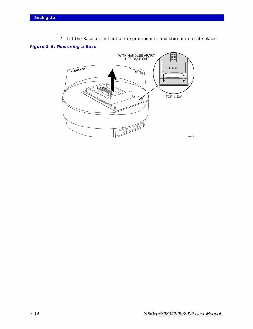
1. Using even pressure, move the handles apart by pushing the Base handle with your thumbs and the sliding handle with your forefingers (see Figure 2-6).
CAUTION: Be sure to apply even pressure as you move the handles apart. If you exert uneven pressure on the handles, you could damage the sliding handle or cause a jam in the tracks. Apply an even force to realign the handles.
Figure 2-5. Aligning the Base
0996-2
GUIDE PIN(1 of 4)
Setting Up
2-14 3980xpi/3980/3900/2900 User Manual
2. Lift the Base up and out of the programmer and store it in a safe place.
Figure 2-6. Removing a Base
0997-2
WITH HANDLES APART,LIFT BASE OUT
TOP VIEW
BASE

Setting Up
3980xpi/3980/3900/2900 User Manual 2-15
4. Turn On the Programmer To turn on the programmer, follow the steps below.
1. Locate the programmer so that the fan on the bottom is not obstructed.
2. Put on the wrist strap and plug it into the ground connector on the programmer’s back panel.
WARNING: Electric Shock Hazard. To help prevent electric shock, the antistatic wrist strap must contain a 1MΩ (minimum) to 10MΩ (maximum) isolating resistor.
3. Connect one end of the AC line cord to the AC receptacle on the programmer’s back panel and the other end to a properly grounded ac outlet.
WARNING: Electric Shock Hazard. To ensure proper grounding and to help avoid the hazard of electrical shock, connect the programmer ONLY to a properly grounded AC outlet. The programmer contains a switching power supply that configures itself to operate on the proper voltage. The power supply accepts voltages ranging from 90 to 264 VAC and frequencies ranging from 48 to 63 Hz.
4. Make sure that a Base is installed in the programmer and the device socket is empty.
CAUTION: Leaving a device in the socket during powerup will cause powerup self-test failures and could damage the device.
5. Turn on the PC, workstation, or terminal. If you will be controlling the programmer from a PC or workstation, make sure that the terminal emulation software (such as TaskLink or HiTerm) is running. If you will be controlling the programmer from a terminal, make sure it is in the proper emulation mode (such as VT-100).
6. Make sure the programmer disk drive is empty, then turn on the power switch on the rear panel.
Make sure the Boot disk is in the programmer disk drive, then turn on the power switch on the rear panel.—3900/2900
7. The Power LED should light. If it does not, turn off the programmer, check the power connections, then turn on the programmer again.
Note: Do not remove the Boot disk while the Self Test or disk drive LED is lit. If you remove the Boot disk during powerup, you must reboot the programmer.

Setting Up
2-16 3980xpi/3980/3900/2900 User Manual
5. Check Self-test ResultsWhen you turn on the programmer, a self-test is performed. While the self-test is in progress, the LEDs are lit as shown:
When the programmer completes powerup, the Self Test LED and disk drive LED turn off and the front panel LEDs illuminate in the patterns shown below, depending on the results of the self-test.
Programmer Passed Self-testIf the self-test was completed successfully, the Power LED lights along with the LEDs for any equipment connected to the Terminal and Remote ports.
Note: Terminal port OK indicates that the programmer detected an RS-232 serial device connected to the Terminal port and a valid connection has been established with that device.
If the correct LEDs are lit, go to “Start-up Screen” on page 2-18. If the corresponding LEDs are not lit, read the next section.
Programmer Did Not Pass Self-testIf the correct LEDs are not lit, refer to the illumination patterns shown below to determine the results of the self-test.
Note: X = don't care condition.
In general, if one or more front panel indicators is blinking after the self-test, there may be a faulty circuit board in the programmer. Contact Data I/O Customer Support for more information.
If the Remote LED and/or Terminal LED should be lit and they are not, check the connections between the programmer and the connected equipment as described in the next section.
Power Terminal Remote Self-TestOn Off Off On
Power Terminal Remote Self-Test Description
On On Off Off Terminal port OK. Self-test finished with no errors.
On Off On Off Remote port OK. Self-test finished with no errors.
On On On Off Remote & terminal ports OK. Self-test finished with no errors.
Power Terminal Remote Self-Test Description
Off X X On Bad power supply.
On Blinking Blinking Blinking Power supply problem; check voltage selector.
On Blinking Off On Bad CPU or EPROM.
On Off Blinking On Bad system RAM.
On Blinking Blinking On Bad serial port DUART.
X X X Blinking Bad LCA.

Setting Up
3980xpi/3980/3900/2900 User Manual 2-17
Checking the Connections Sometimes problems are caused by unconnected cables. Turn off the programmer and check the following:
Power cords—Are all power cords plugged into a live outlet and into the equipment?Cables—Is each cable between the programmer and a peripheral correctly connected to the proper port? Terminal—Is the terminal plugged in and turned on? Are the display controls adjusted to allow viewing? Is the terminal an approved terminal type? (See the list on page 2-6.) Communication—Are the communication parameters set correctly? Is the cable connected to the proper port? Host—Is the host plugged in and turned on? Is the terminal emulation software installed, configured, and running properly? Are the display controls on the monitor adjusted to allow viewing?Disk—Is the Boot disk inserted properly? Base—Is a Base installed correctly? Is the device socket empty? (A base must be installed and the socket must be empty.)
After you check everything described above, reboot the programmer using one of these methods (a powerup self-test is performed in either case):
Turn off the programmer, wait a few seconds, then it on turn again. Press ESC CTRL+W.
If the Start-up screen (shown in Figure 2-8) is displayed, the programmer was booted successfully. Continue with “Start-up Screen” on page 2-18.
If the Start-up screen is not displayed or if you see random characters, the programmer is not communicating properly with your controlling terminal/workstation. The baud rates of the programmer and the controlling equipment may not match. Follow the procedure in the next section to run the AutoBaud function to “sync up” the baud rates.
AutoBaud and Baud Rates AutoBaud determines the baud rate of the equipment connected to the programmer's Terminal port and sets the programmer's baud rate to match.
Note: AutoBaud is enabled as a factory default.To run AutoBaud, press BREAK, then A. After running AutoBaud, you should see the Start-up screen. If so, go to the next step, “Start-up Screen.” If you do not see the Start-up screen, return to “Checking the Connections.”
When to Use AutoBaud?Normally, you can set the communication parameters on the controlling PC/workstation/terminal to match the programmer's baud rate. Use AutoBaud when you will not be able to set the controlling equipment's baud rate to match the programmer's. For example, use AutoBaud to control the programmer with a terminal that cannot operate at 9600 baud. Set the terminal's baud rate as close to 9600 as possible, then run AutoBaud when the programmer boots up.

Setting Up
2-18 3980xpi/3980/3900/2900 User Manual
6. Start-up Screen The Start-up screen is displayed after the programmer completes its powerup self-test successfully. The version and configuration information for the programmer along with the current and default terminal types are displayed.
How to Configure Programmer Parallel Port (TaskLink for Windows Only) 1. Connect the programmer to the parallel port on your PC using the parallel
port cable supplied with your programmer.
Note: If your PC has been more than one parallel port, note which port is used.
2. Connect the programmer to the serial port on your PC using the serial port cable supplied with your programmer.
Note: Because some operations are not supported on the parallel port, it is necessary to connect the programmer and PC via their serial port as well. TaskLink uses the parallel port if Programmer Parallel Port is enabled (see Step 4 below). If the operation is not supported on the parallel port, TaskLink switches to the serial port to complete the operation.
3. Start TaskLink and select Options from the System menu.
4. If running Windows 95/98, on the Port Settings tab, enter a check to enable Programmer Parallel Port. From the drop-down list, select the parallel port that matches the port used on the PC.
5. Enter the correct Port Address.
Note: Most computer systems have default settings of LPT1 and address 378.
6. If running Windows NT, on the Port Settings tab, enter a check to enable Programmer Parallel Port. Click Configure.
7. On the UniSystem Parallel Port Setup dialog, from the drop-down list, select the parallel port that matches the port used on the PC. Click Configure.
8. On the Port Settings tab, click OK to return to the TaskLink main screen.
9. On the TaskLink main screen, click the Establish Contact icon in the upper left corner.
10. If the programmer is properly connected via the parallel port, the following message is displayed:
Figure 2-7. Connection Established Message

Setting Up
3980xpi/3980/3900/2900 User Manual 2-19
If the current terminal type is correct, press ENTER and go to “Set Up High Speed Download” on page 2-20 if you will be using high speed download, or go to “Install Devices” on page 2-22.
Selecting a New Terminal TypeTo change the current terminal type and/or the default terminal type, follow these steps.
1. When the programmer prompts Do you want to select a new terminal type? (Y/N) [N]: press Y, then ENTER.
2. The default and current terminal types and a list of the available terminal types is displayed. Enter the number corresponding to the terminal type you want to use, then press ENTER.
If the screen is blank or if random characters are displayed, the Terminal type configuration is incorrect. Turn off the programmer, turn it on again, then select the correct terminal.
3. After you change the terminal type for this current session, the programmer responds with the following prompt: Save terminal type as power on default? (Y/N) [N]
4. To save the terminal as the powerup default, press Y, then ENTER.
To use this terminal type for this session only, press N, then ENTER.You are returned to the Main Menu.
Figure 2-8. Typical Start-up Screen For HiTerm Users

Setting Up
2-20 3980xpi/3980/3900/2900 User Manual
7. Set Up High Speed Download (optional)With the programmer configured for High Speed Download, you can download files from the PC to the programmer, significantly reducing the transfer time for a large data file.
Note: To obtain the best results, we recommend you use a 486 or higher PC.
During a high speed download, the data file on the PC is translated into a special binary format and compressed.
Note: When using the serial port, both compression and an increase in speed to 115.2K baud occur. When using the parallel port, the baud rate does not increase.
To use this feature, you must control the programmer from a PC, the PC must be connected to the programmer's Remote or Parallel Port, and you must use TaskLink or HiTerm as your terminal emulation software.
High Speed Download supports the following formats:Formatted Binary (10)Motorola EXORciser (82)Motorola EXORmax (87)Motorola 32-bit (95)Intel INTELLEC (83)Intel MCS-86 (88)Intel Hex-32 (99)JEDEC (full) (91)
During a download, the data file is downloaded to the programmer. After the download, the baud rates on the PC and programmer are restored to their original values.
Note: A temporary copy of the data file is compressed; your original data file is not changed.
Setting Up High Speed Download with TaskLink for Windows/DOSHigh Speed Download is enabled as the default in TaskLink V1.7 and higher.
If needed, enable High Speed Download by following these steps:
1. From TaskLink’s Main Menu, select Options, Set Preferences. Select the box next to the Enable High Speed Download option to enable it.
Note: Settings are retained once saved.
Setting Up High Speed Serial Download with HiTermFollow these steps to connect your PC to the programmer's Remote port and configure the programmer to run in Terminal mode from the Remote port.
1. Start HiTerm.
2. Power up the programmer. If the programmer is already powered up, reboot it by pressing ESC CTRL+W. Boot up as normal.
3. From the Main Menu, press M C E C to get to the Communication Parameters screen.

Setting Up
3980xpi/3980/3900/2900 User Manual 2-21
4. Move the cursor to the High Speed Download field, then press Y. The programmer displays: Hit return to switch user menu port, ^Z to abort.
5. Press ENTER. You will see no response on the screen.
The User Menu Port parameter is set to R, which configures the programmer to send its user interface data to the Remote port. The Terminal port is the factory default for the User Menu Port. (User interface data includes screens, menu information, and online Help.
6. Move the cable connecting the programmer and the PC from the Terminal A port to the Remote port.
The Terminal LED should go out and the Remote LED be lit. If the Remote LED does not light, turn off the programmer, reconnect the PC cable to the Terminal port, then return to step 1.
7. Press CTRL+R to redisplay the Communication Parameters screen.
If this screen is not displayed, turn off the programmer, reconnect the PC cable to the Terminal port, then return to step 1.
8. Press F1 to display the Main Menu, then continue with the next step.
If the Main Menu is not displayed, turn off the programmer, reconnect the PC cable to the Terminal port, then return to step 1.
High Speed Download is now enabled for this session.
Changing the Powerup Defaults If you do not save the changes you made, you can use High Speed Download for the current session but you must repeat the procedure to enable it the next time you turn on the programmer.
To make High Speed Download part of your powerup defaults, follow the steps below (for the complete list of powerup defaults, see page 4-3).
1. From the Main Menu, press M C S to display the Save System Parameters screen. Up to ten configuration files are displayed.
2. Press 1 ENTER. The programmer displays: Parameter Entered.
3. Press ENTER to save the current settings as the Powerup Defaults. The action symbol rotates as the programmer saves the settings.
When finished, the programmer displays the following message: System parameters saved.
High Speed Download will now be available whenever you turn on the programmer.
To learn how to download files to the programmer using High Speed Download, see the tutorial Session on page 3-26.

Setting Up
2-22 3980xpi/3980/3900/2900 User Manual
8. Install Devices Use the following procedures to install devices in the programmer's Base:
Inserting a DIP Device into a DIP Base . . . . . . . . . . . . . . . . . . . . . . . . 2-22Installing a MatchBook into a Base . . . . . . . . . . . . . . . . . . . . . . . . . . . 2-23Inserting a PLCC or LCC Device into a MatchBook . . . . . . . . . . . . . . . . . 2-24Inserting an SOIC Device into a MatchBook . . . . . . . . . . . . . . . . . . . . . 2-25Inserting a PGA Device into a PGA Base . . . . . . . . . . . . . . . . . . . . . . . 2-26
Inserting a DIP Device into a DIP Base1. Install the DIP Base.
2. Unlock the socket by pulling up on the socket lever.
3. Insert the DIP device into the socket. Bottom justify the device as shown in Figure 2-9. If the device is not bottom justified, the programmer cannot read or program the device.
4. Lock the device into place by pressing the socket lever down.
Figure 2-9. Inserting a DIP Device into the DIP Base
0548-2
SOCKET LEVERSUNLOCKED
PIN 1SOCKETLEVERSLOCKED

Setting Up
3980xpi/3980/3900/2900 User Manual 2-23
Installing a MatchBook into a Base The MatchBook device carrier holds a device in place on the Base. When the device is locked into place, the conductive pad in the Base forms a conductive path between the pin drivers in the programmer and the device in the MatchBook.
The following procedure describes how to use a MatchBook and how to insert and remove devices from a MatchBook.
1. Insert the Base into the programmer and lock it into place.
2. Select the appropriate MatchBook, open it 90º, set the front edge under the two locking tabs at the front of the Base, then lower the back edge of the MatchBook into place on the Base. See Figure 2-10.
3. Insert the device into the MatchBook as described later in this section.
4. Finally, close the MatchBook and press the retaining latch forward with your thumb until the latch snaps into place as shown in Figure 2-11.
CAUTION: To prevent premature wear on the conductive pad, do not place excessive force on the top of the MatchBook.
Figure 2-10. Inserting a MatchBook into the Base
Figure 2-11. Closing the MatchBook
0537-4
FRONT EDGE(Under locking tabs)
BACK EDGE
LOCKING TAB
MATCHBOOK
0539-5
44 PIN PLCC

Setting Up
2-24 3980xpi/3980/3900/2900 User Manual
Inserting a PLCC or LCC Device into a MatchBook Use the following procedure to insert a PLCC or LCC device into a MatchBook.
1. Select the appropriate MatchBook and Base. For example, if you are using a 44-pin PLCC device, select the 44-pin PLCC MatchBook and the PLCC Base.
2. Insert the appropriate Base into the programmer (see page 2-12).
3. Insert the appropriate MatchBook into the Base (see page 2-22).
4. Position the device so that pin 1 is near the handle on the Base (see Figure 2-12). A small dot molded into each MatchBook is available to help you align your device. There is also a beveled corner on the PLCC/LCC MatchBook to help you align devices in which pin 1 is indicated with a chamfered corner.
5. Insert the device into the open MatchBook.
6. Close the MatchBook and press the retaining latch forward with your thumb until the latch snaps into place, as shown in Figure 2-11.
CAUTION: Do not place excessive force on the top of the MatchBook, as this may cause premature wear on the conductive pad.
Figure 2-12. Inserting a Device into the PLCC or LCC Base
0538-4
CHAMFERED CORNER
PIN 1
RETAINING LATCH
DOT
CHAMFER

Setting Up
3980xpi/3980/3900/2900 User Manual 2-25
Inserting an SOIC Device into a MatchBookUse the following procedure to insert an SOIC device into the SOIC MatchBook.
1. Install the SOIC Base into the programmer (see page 2-12).
2. Select the appropriate MatchBook for the device you will be using and install it in the SOIC Base (see page 2-23).
3. Position the SOIC device so that pin 1 is up and to the right as you view it from the top.
4. Insert the SOIC device into the open MatchBook so that the device is flush against the left side of the MatchBook. Make sure the device is positioned between the six alignment fingers and not on top of them.
Note: The unused portion of the socket will be on the right as you view it from the top.
The small, round dots along the top of the opening, as shown in Figure 2-13, indicate the location of pin 1 for the various sizes of SOIC devices the SOIC MatchBook will accept.
5. Finally, close the MatchBook and press the retaining latch forward with your thumb until the latch snaps into place, as shown in Figure 2-11.
Figure 2-13. Inserting an SOIC Device
0568-4
LEFT JUSTIFY DEVICEIN SOCKET
PIN 1
ALIGNMENTFINGER (1 OF 6)

Setting Up
2-26 3980xpi/3980/3900/2900 User Manual
Inserting a PGA Device into a PGA BaseThe PGA Base can accommodate PGA packages up to 15 x 15 pin arrays. Use the following procedure to insert a PGA device into the PGA Base.
Note: When you insert a PGA device into the PGA Base, pay particular attention to the orientation and positioning of the device.
1. Install the PGA Base into the programmer (see page 2-12).
2. Unlock the PGA socket by lifting up on the socket lever.
3. Insert the device into the PGA socket. Make sure the PGA device is bottom justified and that pin 1 of the device is against the left side of the socket. Figure 2-14 shows the proper alignment of a PGA device.
4. Push the socket lever down to lock the PGA device into the PGA socket.
Figure 2-14. Orienting a PGA Device in the PGA Base
0566-5
FR
EE
LOC
KFR
EE
LOC
K
ARROW MEANS BOTTOM JUSTIFY
DEVICE IN SOCKET
NUMBERS AND SMALLARROWS INDICATE
PIN 1 LOCATIONS
68/84 PIN PGA
88 PIN PGA
44 PIN PGA
1
1
1
28 PIN PGA1
SOCKET LEVER PGA SOCKET

Setting Up
3980xpi/3980/3900/2900 User Manual 2-27
Installing a PPI Adapter into the PPI Base Perform the following procedure and refer to the illustrations to install a PPI adapter in the PPI Base.
CAUTION: Do not touch the exposed SPA pins on the PPI base with anything but a cleaning cloth. Contamination of the pins could lessen programming reliability. To avoid damage to the device, do not install it in the adapter until the adapter is securely installed in the Base.
Do not disassemble the PPI base; doing so could cause the pins to drop out. 1. Install the PPI Base in the programmer (see page 2-12).
Note: If the adapter socket has a high profile, see the next section.2. Raise the removable base door until it rests in the upright position.
3. Position the adapter so the retaining latch end faces toward the latches near the front of the Base. Slide the rear of the adapter into the back of the Base. The alignment holes in the front corners of the adapter should slide onto the plastic guide pins.
4. Lower the base door over the PPI adapter.
5. Press down on the door until the latches snap into place over the door. Make sure that both latches are securely in place.
2412-3
BASE DOOR RETAININGLATCH
ADAPTER
LATCHES
SPA PINS
GUIDEPIN(1 of 2)
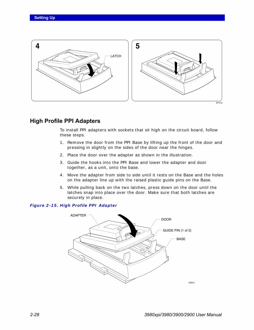
Setting Up
2-28 3980xpi/3980/3900/2900 User Manual
High Profile PPI AdaptersTo install PPI adapters with sockets that sit high on the circuit board, follow these steps.
1. Remove the door from the PPI Base by lifting up the front of the door and pressing in slightly on the sides of the door near the hinges.
2. Place the door over the adapter as shown in the illustration.
3. Guide the hooks into the PPI Base and lower the adapter and door together, as a unit, onto the base.
4. Move the adapter from side to side until it rests on the Base and the holes on the adapter line up with the raised plastic guide pins on the Base.
5. While pulling back on the two latches, press down on the door until the latches snap into place over the door. Make sure that both latches are securely in place.
Figure 2-15. High Profile PPI Adapter
LATCH
2413-2
1326-2
BASE
DOORADAPTER
GUIDE PIN (1 of 2)

Setting Up
3980xpi/3980/3900/2900 User Manual 2-29
Inserting Devices in a PPI AdapterPPI adapters accept a variety of device package types and pin configurations. The following figures show common device packages and the proper device orientation in the adapter. An icon on each adapter indicates proper device orientation.
TSOP DevicesTSOP (Thin Small Outline Package) devices have two different pinouts:
Standard pinout—the icon represents pin 1 with a circle in the upper-left corner of the device.Reverse pinout—the icon represents pin 1 with a triangle in the upper-left corner of the device.
To install a TSOP device in a PPI Base, follow the steps below and refer to the illustration.
1. Press down on the outer edges of the socket.
2. While holding the socket edges down, drop the device into the socket.
3. Release the socket edges. The device should be secured.
To remove a device, press the socket edges down and lift it out.
Figure 2-16. Inserting a TSOP Device in a PPI Base
1327-1
PIN 1
TSOPSOCKET
PIN 1 OF SOCKET
DEVICE
STANDARD PINOUT ICON
REVERSE PINOUT ICON

Setting Up
2-30 3980xpi/3980/3900/2900 User Manual
QFP DevicesOrient pin 1 of QFP (Quad Flat Pack) devices according to the icon or indicator on the adapter.
Figure 2-17. Inserting a QFP Device in a PPI Adapter
1328-2
QFP SOCKET
PIN 1
DEVICE
PIN 1

Setting Up
3980xpi/3980/3900/2900 User Manual 2-31
SOIC DevicesWhen you insert SOIC (Small Outline Integrated Circuit) devices, make sure pin 1, represented by the notch or the circle indented into the package at one end of the device, is to the left, as shown in the illustration.
SDIP DevicesOrient SDIP (Shrink DIP) devices in the socket with pin 1 at the top left and with the bottom of the device aligned with the bottom of the socket.
Figure 2-18. Inserting an SOIC Device in a PPI Adapter
Figure 2-19. Inserting an SDIP device in a PPI Adapter
2755-1
PIN 1
PIN 1
ORIENTATION ICON
PIN INSULATION BLOCK
PROGRAMMING BLOCK
CIRCUIT BOARD
SOIC DEVICE
2414-1
SDIP SOCKET
SDIP DEVICE
PIN 1
PIN 1
SDIP ORIENTATIONICON

Setting Up
2-32 3980xpi/3980/3900/2900 User Manual
Inserting Other DevicesThe programmer must be fitted with a Base and adapter appropriate for the device you are using. When you insert a device into an adapter socket, consult the illustrations on the adapter to determine device orientation. Most devices are keyed so that they can fit into the socket only one way. For more information, refer to the documentation included with the adapter.
9. Preventive Maintenance Cleaning the Fan
Operate your programmer where the vent over the fan will not become blocked, and remove any dust or dirt that accumulates on the fan vent.
Conductive PadThe conductive pad (see Figure 2-20) is a key element in the MatchBook technology. To help keep yields high and prolong the life of the pad, keep it free of dirt and other contamination. We recommend you inspect and clean it at least every 1000 device insertions or once a month, whichever comes first.
The life of the pad also depends on the pin count and package type of the device you are using. Different tolerances may result in different life cycles for the pad. An increase in device insertion errors or continuity errors or a sudden drop in programming yields may indicate the pad needs to be replaced.
Note: You may notice an indentation in the middle of the pad after a number of insertions. The indentation is normal and does not degrade the performance of the MatchBook. It is also normal for the pad to show signs of discoloration as it is used.
Cleaning the PadBlow air over the pad to clean it. If you use compressed air, direct the air stream from the front or back of the Base, not from the side.
CAUTION: To avoid lifting the pad off the circuit board, do not blow air from the side of the pad.
Figure 2-20. Conductive Pad
2801-1
CONDUCTIVE PADDO NOT REMOVE

Setting Up
3980xpi/3980/3900/2900 User Manual 2-33
To further clean the pad, apply a small amount of isopropyl alcohol on a cotton swab and with a rolling motion, gently wipe off the pad. Make sure the pad is free of any cotton filaments left over after cleaning.
CAUTION: Do not use petroleum- or freon-based products to clean the pad. These substances will cause premature deterioration of the pad material.
Replacement Pad KitsTo minimize downtime, the Base was designed to allow you to replace pads quickly and easily. Contact Customer Support to order replacement pad kits.
SPA Block and BaseThe following messages during device operations could indicate dirt in the SPA block or Base adapter.
ID ErrorContinuity ErrorBase Adapter not InstalledDevice Insertion ErrorOvercurrent ErrorBase/Adapter Relay Failure
Follow these guidelines to prevent the accumulation of dirt:When the programmer is not in use, keep the SPA block covered with a Base. When Bases are not in use, store them in an uncontaminated area to keep them clean to prevent contamination of the SPA block.Whenever you remove or replace a Base, clean the SPA block with a brush. At least once a week, inspect the SPA block and Base for contamination of dirt or oil. Clean them as described below.

Setting Up
2-34 3980xpi/3980/3900/2900 User Manual
Cleaning Procedure1. Blow filtered, compressed air across the SPA block (see Figure 2-21).
2. Mildly dampen a small section of a lint-free cloth with a DeoxIT pen (Data I/O P/N 570-5500-901) and gently rub the dampened cloth across all the pins on the SPA block.
3. Using a clean section of the lint-free cloth, gently wipe the surface again.
4. To check that the pins spring up to their normal upright position, push a base down on the SPA pins a few times.
5. Clean all surfaces of the Base using filtered compressed air and a lint-free cloth dampened with DeoxIT, if needed.
Figure 2-21. SPA Block and Base
2803-2
SPA BLOCK
BASE

Setting Up
3980xpi/3980/3900/2900 User Manual 2-35
10. What To Do Next TimeUse the following procedure to run subsequent sessions, if you suspect the programmer was moved, or if the programmer has not been used for awhile.
1. Check the power cords and cables between the programmer and the connected equipment.
2. If you are controlling the programmer from a PC or workstation, make sure it is on and that the terminal emulation software (such as TaskLink or HiTerm) is running.
If you are controlling the programmer from a terminal, make sure it is on. If you are using TaskLink, select VT100 on Programmer Port from the Utilities menu.
3. To boot from the MSM hard drive, make sure the programmer disk drive is empty.
Insert the Boot Disk in the programmer disk drive. —3900/2900
4. Insert the Base into the programmer and lock it into place.
5. Turn on the programmer.
6. Verify the terminal type when the Start-up screen is displayed.
7. Install a device.
8. Select a device operation. (See the tutorial sessions in Chapter 3.)
9. If prompted, remove the currently installed disk and insert the disk that is requested.

Setting Up
2-36 3980xpi/3980/3900/2900 User Manual
11. Using the Mass Storage Module (MSM)To boot from the MSM hard drive, ensure that the programmer disk drive is empty, then turn on the programmer.The MSM is partitioned into four logical drives with the following specifications:
Drives C and D are reserved for user data, and drives H and I are reserved for system use. Although drives H and I can be written to and read from, we STRONGLY suggest you use only C and D to store your data. Periodically copy the data on the C and D drives to use as a backup if needed.
Drives C and D can be used for same file operations that can be performed using the floppy drive except for these two file operations:
Format Disk—Format only C and D. Formatting H or I will render your programmer inoperative until you restore them from the floppy disks.Duplicate Disk—Drives C, D, H, and I cannot be duplicated using this command.
Drive Storage Max. No. of Files Data Type
C 31 MB 512 User dataD 31 MB 512 User dataH 7 MB 320 System dataI 10 MB 320 System data

3980xpi/980/3900/2900 User Manual 3-1
3 Getting Started
Before you start the Sessions in this chapter, read Chapters 1 and 2 and make sure the programmer is connected and working correctly. The Sessions will help you learn the basics of programmer operation. For more information about commands, refer to Chapter 4 and to online help.
For TaskLink Users (Windows and DOS)1. Programming a Device. . . . . . . . . . . . . . . . . . . . . . . . . . . . . . . . . . . 3-2
For HiTerm Users (Terminal Mode)2. Navigating Through the Programmer Menus . . . . . . . . . . . . . . . . . . . 3-103. Selecting a Device . . . . . . . . . . . . . . . . . . . . . . . . . . . . . . . . . . . . 3-154. Selecting a Keep Current Algorithm. . . . . . . . . . . . . . . . . . . . . . . . . 3-175. Loading Data from a Device . . . . . . . . . . . . . . . . . . . . . . . . . . . . . . 3-206. Loading Data from Disk . . . . . . . . . . . . . . . . . . . . . . . . . . . . . . . . . 3-237. Selecting a Translation Format . . . . . . . . . . . . . . . . . . . . . . . . . . . . 3-258. Loading Data from a PC Using HiTerm . . . . . . . . . . . . . . . . . . . . . . . 3-269. Loading Data from a Host . . . . . . . . . . . . . . . . . . . . . . . . . . . . . . . 3-2810. Editing Data . . . . . . . . . . . . . . . . . . . . . . . . . . . . . . . . . . . . 3-3111. Programming a Memory Device. . . . . . . . . . . . . . . . . . . . . . . . . . . 3-3312. Verifying a Device . . . . . . . . . . . . . . . . . . . . . . . . . . . . . . . . . . . . 3-35
Outline of the Programming OperationSelect the manufacturer and part number of the device you will be using so the programmer can perform device operations with the appropriate programming algorithm.
The Load Data operation moves device data from a master device, hard drive, floppy disk drive, or network into programmer RAM.
The Program Device operation transfers the device data in RAM into the device in the socket using the device’s programming algorithm.
The verify operation (included with programming) compares the data in a programmed device to thedata in programmer RAM. Additional verify operations provide information about programming errors. Logic device verification can include functional testing.
1. Select Device
2. Load Device Data
3. Program Device
4. Verify Device
=
Device Manufacturer &Device Part Number
Data inDevice
Programmer RAM
Programmer RAM
Device in Socket
Data inRAM
Device Data

Getting Started
3-2 3980xpi/3980/3900/2900 User Manual
Session 1: Programming a Device Using TaskLinkThis tutorial is designed to help you become familiar with TaskLink screens and the steps you will use to program a device. For this Session, you will use TaskLink in simulation mode and do not need to have your programmer connected.
For TaskLink for Windows1. From the Setup menu, select Select Device.
2. Scroll through the list of device part numbers until the one you want is highlighted.Click Select.
.
3. From the Setup menu, select Programmer Properties..

Getting Started
3980xpi/3980/3900/2900 User Manual 3-3
4. Select the General tab, and enter the parameters that you wish to use. These parameters determine what device operations are performed before, during andafter programming.
5. Now select the Memory tab. Enter the parameters to specify how and where the data is loaded in programmer RAM.
To ensure consistent sumcheck, you can preload add address locations into RAM with a known hexadecimal value (many data files do not contain data for every memory address.) For further information, see the online help.
6. The next step is to load programmer RAM with the data to be programmed into the device. To do this, from the Data menu, select Load RAM from... PC/Network File.

Getting Started
3-4 3980xpi/3980/3900/2900 User Manual
7. The following will appear; Click the Browse button to find your file.
8. Search for and select a file from any drive accessible from your PC.
9. Before/after choosing the file, choose the Translation Format from the drop-down menu located on the same window- Load Programmer RAM from PC/Network File.
10.When the file is successfully loaded into the programmer RAM, a box displays the Checksum of RAM.

Getting Started
3980xpi/3980/3900/2900 User Manual 3-5
11. From the Process menu, select Select Process. A checkmark in the selection box indicates that the process will be performed. When the appropriate boxes are selected, click OK.
12. From the Process menu, select Process Devices.
13. In the Pass Limit field, enter the number of devices you want to program. To program an unlimited number of devices, leave this value set to 0.
The optional Session ID tracks who programmed what devices. See online help for further details.

Getting Started
3-6 3980xpi/3980/3900/2900 User Manual
14.You will be prompted when to insert the device to be programmed.
Click Start when you are ready to commence programming..
15.During the processing, the number of successfully programmed devices and total number of attempts is displayed. The Last Device box displays “Pass” on a green background or a message that describes failure on a red background.
Click End Session when you have finished or need to quit.

Getting Started
3980xpi/3980/3900/2900 User Manual 3-7
For TaskLink for DOS:
1. From the TaskLink directory, type tl as (simulation mode), then press ENTER. (To run TaskLink when you want to actually program a device, type tl a, then press ENTER.)
2. From the Setup menu, select Select Device.
3. Scroll through the list until the manufacturer of the device you want to use is highlighted, then click OK.
4. Scroll through the list of device part numbers until the one you want is highlighted, then click OK.
5. From the Setup menu, select General Parameters. These parameters determine what device operations are performed before, during, and after programming.To learn the parameter’s function, highlight it, then press F1. The Help topic is displayed.

Getting Started
3-8 3980xpi/3980/3900/2900 User Manual
6. From the Setup menu, select Memory Parameters to specifyhow and where data is loaded in programmer RAM.To ensure a consistent sumcheck, you can preload all address locations into RAM with a known hexadecimal value (many data files do not contain data for every memory address). To do this, select Specific under Automatic RAM Fill and enter a value (usually 00 or FF) to be placed in RAM before a file is loaded.To learn about I/O Offset, highlight it, then press F1 to display Help.
7. The next step is to load programmer RAM with the data to be programmed into the device. In this example, the data is stored in a file on a disk, so select Load RAM from PC Disk File.
8. Press F2 or click on the down arrow at the right end of the dialog box to display the Data File selection box.
9. Search for and select a file from any drive accessible from your PC.

Getting Started
3980xpi/3980/3900/2900 User Manual 3-9
10. From the Data menu, select Translation Format. Highlight the format of the file you will load into RAM, then click OK.
11.When the file is successfully loaded into programmer RAM, a green box displays the Checksum of RAM.
12. From the Program menu, select Select Process. An X in the selection box indicates that process will be performed. When the appropriate processes are selected, click OK.
13. From the Program menu, select Process Devices. In the Pass Limit field, enter the number of devices you want to program. To program an unlimited number of devices, leave this value set to 0. The optional Session ID tracks who programmed what devices. See the Session Data Logging topic in Help for more information.
14. You will be prompted when to insert the device to be programmed. See page 2-22.
15.During processing, the number of successfully programmed devices and total number of attempts is displayed. The Last Device box displays “Pass” on a green background or a message that describes a failure on a red background.
16.At the end of the programming session, the Session Statistics Display screen is displayed.

Getting Started
3-10 3980xpi/3980/3900/2900 User Manual
Session 2: Navigating Through the Programmer MenusThis session describes the programmer menus and the online Help in Terminal Mode.—3980/3900/2900
See online help for description of the programmer menus in TaskLink for Windows.
Programmer Main MenuPower up the programmer. After you select the terminal type, the Main Menu is displayed. See Figure 3-1. The Main Menu, as are most programmer screens, is divided into five areas: status window, message bar, command window, dialog window, and reminder bar.
Status Window The status window, which occupies the top three lines of the screen, displays important system information, such as:
Name of the data file (FILE.JED in Figure 3-1) Amount of User RAM (2176KB) Version number of the Algorithm/System disk (X.XX and Y.YY) Device manufacturer and part number (TI and 20L8A) Data translation format (JEDEC full selected)
Message BarThe message bar displays system and error messages. Also located in the message bar is the action symbol, which rotates during an operation to indicate that the programmer is busy.
Command WindowThe command window displays the menu name in uppercase letters and the available commands in upper- and lowercase letters below the menu name.
Figure 3-1. Main Menu
Status Window
Message Bar
Command Window
Dialog Window
Reminder Bar

Getting Started
3980xpi/3980/3900/2900 User Manual 3-11
Dialog WindowThe dialog window, the largest area on the screen, displays different information and system parameters, depending on the selected command.
Reminder BarThe reminder bar describes the function keys that are available.
Moving AroundPressing the arrow keys moves the cursor in the direction indicated on the key. The cursor will wrap around when it has reached the edge (top, bottom, left, right) of a window.
Selecting a Menu ItemTo select a command, either move the cursor to the menu item and press ENTER, or press the first letter of the menu item. For example, to test the programmer, select the Self-test command on the More Commands menu. To access the More Commands menu, move the cursor to the More Commands menu item and press ENTER, or press M. The More Commands menu is displayed. If it is not displayed, press F1 and try again.
Figure 3-2. More Commands Menu Screen

Getting Started
3-12 3980xpi/3980/3900/2900 User Manual
Move the cursor to the Self-test menu item (press the down arrow), then press ENTER or S to run the command. The Self-test screen is displayed.
Using Key FunctionsSome of the programmer's functions may be performed by pressing a key or a combination of keys. To use the CTRL key, hold it down, then momentarily press the second key. The key functions are listed below with their corresponding keystroke sequence.
In most cases, press the F2 key to exit a menu selection. If this does not work, you can press the CTRL+Z keys to cancel the operation.
Figure 3-3. Self-test Screen
Keystrokes DescriptionF1 Return to the Main MenuF2 Go to the previous menuF3 or ? Display online Help for the current menu and cursor positionF4 Display the Optional Parameters screenENTER Execute highlighted command SPACE Toggle a parameterCTRL+N Display next pageCTRL+P Display previous pageCTRL+R Repaint screenCTRL+Z Halt current operation ESC CTRL+T Enter/exit transparent mode with host computer ESC CTRL+J Start/stop job file recording ESC CTRL+W Restart the programmer (warm boot) BREAK A Execute AutoBaud ALT+F1 Exit HiTerm

Getting Started
3980xpi/3980/3900/2900 User Manual 3-13
Selecting Online HelpOnline Help screens provide both general Help and context-sensitive Help (information specific to a particular field on the screen). To access Help, move the cursor to the item you want to learn about, then press either F3 or ?. The Help screen is divided into four sections: the key listing, general Help, context-sensitive (specific) Help, and the reminder bar. A sample Help screen is shown in Figure 3-4.
Key ListingThe key listing provides a quick summary of some of the most often used key commands. Key combinations displayed with a dash between them, such as CTRL-P, indicate you should press and hold the first key, then press the second key. Key combinations displayed with a space between them, such as ESC CTRL-T, indicate you should press and release the first key, then press the key combination.
General HelpThe general Help text describes the next higher command or menu. The general Help changes when you move to another menu level, for example, when you leave the Self-test screen and return to the More Commands menu.
Context-sensitive HelpDisplayed in reverse video, the context-sensitive Help describes the item the cursor was on when you called the Help function. The information in this field changes when you move the cursor to a different location on the screen.
Reminder Bar Displayed on the bottom line of the screen, the reminder bar shows which function keys you can use to exit Help.
Accessing Online Help for System MessagesOnline Help is available for non-fatal system messages, which result from situations that do not interrupt the programmer's operation. Fatal messages, which result from situations that do interrupt the programmer's operation, are listed and described in Chapter 6.
Figure 3-4. Areas of the Help Screen
Key Listing
General Help
Context-sensitive Help
Reminder Bar

Getting Started
3-14 3980xpi/3980/3900/2900 User Manual
Non-fatal error messages are generally displayed in the message bar. To display the online Help for a message, press F3 or ?. Exit the message Help screen as you would any Help screen.
Accessing Device-specific Online InformationAfter you select a device, if the Display Device Footnote feature is enabled (the default) any online device-specific information for that device is displayed. You can enable Display Device Footnote in the More Commands/Configure System/Edit/Programming Parameters screen.If the Display Device Footnote is disabled, a message prompts you to press F3 or ? to display any available device-specific information. Press CTRL+N to view the next screen; press CTRL+P to view the previous screen.
Exiting HelpTo exit a Help screen, including the device footnote screen, press either F1 (to return to the Main Menu) or F2 (to return to the screen from which you entered Help).
ReviewIn this Session you learned how to move through the programmer's interface. To select menu items, either press the first letter of the command, or move the cursor to the command then press ENTER.To return to the Main Menu, press F1.To access previous screens, press F2. To access online Help, press either F3 or ?.

Getting Started
3980xpi/3980/3900/2900 User Manual 3-15
Session 3: Selecting a DeviceThis Session describes how to select the manufacturer and part number of the device you are using. You should have completed Session 2, which introduces you to the programmer's interface.If you do not have an AMD 27256 (the device used for this Session), substitute the manufacturer and part number of the device you want to use. (The device you use may not have the same capabilities as the AMD 27256. For example, the AMD 27256 supports Electronic ID while the Hitachi 27256 does not.)
Select a ManufacturerFrom the Main Menu, choose the Select Device Command. You can either press S or move the cursor to the Select Device menu item and press ENTER. The Manufacturer List screen (similar to Figure 3-5) is displayed.
The text in the upper-right corner of the screen shows how many screens (pages) of manufacturers there are and what page you are on. To go to the previous page of manufacturers, press CTRL+P. To go to the next page, press CTRL+N. The list is in alphabetical order. Some manufacturers are listed by their commonly used abbreviations (such as AMD for Advanced Micro Devices).
The Device Type field allows you to filter out certain device types. Press Space to cycle through the three settings: All, Memory & Emicros, or Logic Only. When you select a manufacturer, the programmer displays only devices that fit the filter you selected.This Session uses a 27256, an EPROM. Move the cursor to the Device Type field, press SPACE to cycle through the device types until Memory & Emicros appears in the field. Page through the screens until you find AMD. Move the cursor to the Manufacturer field, enter the number to the left of AMD, and press ENTER. The Part list, similar to the one in Figure 3-6, is displayed.
Figure 3-5. Device Manufacturer Selection Screen

Getting Started
3-16 3980xpi/3980/3900/2900 User Manual
Select a Device Part NumberSelecting a device part number is similar to selecting a device manufacturer: find the item in the menu and enter the number beside the item. The part numbers are arranged alphanumerically. If you do not find the 27256 number on this screen, you may need to view the next screen to view more supported devices for this manufacturer. Page through the screens and find 27256. Type the number enclosed in parentheses (for example, in Figure 3-6, you would type 31), then press ENTER.The programmer loads the algorithm for the device you selected, in this case an AMD 27256. (The action symbol, located at the left end of the message bar at the top of the screen, rotates while the programmer loads the algorithm.)
Accessing Device-specific Online InformationSome devices have information relating to their use and programming. When you select a device that has footnotes or other device-specific information, the Display Device Footnote feature (enabled as the default) displays the information. If this feature is not enabled, the programmer prompts you to press F3 or ? to view the information. (You can enable Display Device Footnote under More/Commands/Configure System/Edit/Programming Parameters.)If there is more than one screen of device-specific information, press CTRL+N to view the next screen of information. Press CTRL+P to view the previous screen of information. Press F2 to exit the screen.The device used in this Session does not require any online information.
ReviewTo select a device, you must first select the Manufacturer of the device, then the part number of the device.Some devices have special information available online that can be viewed after a device is selected.
Figure 3-6. Part Number Selection Screen

Getting Started
3980xpi/3980/3900/2900 User Manual 3-17
Session 4: Selecting a Keep Current AlgorithmThis Session describes how to select a device that is supported by a Keep Current algorithm you downloaded from the Data I/O Web site or the Keep Current Bulletin Board System (BBS). See Appendix C for more information.
The Keep Current algorithm(s) should be on a 3.5-inch disk formatted in your programmer.
Note: The device you use may not have the same capabilities as the device used in this Session.
Insert the Keep Current Algorithm DiskInsert the 3.5-inch disk containing the Keep Current algorithm(s) into the programmer disk drive.
Select the Keep Current OptionThe device selection process is a two-step process: first the programmer displays a list of the available Keep Current algorithms, then you select the algorithm.
From the Main Menu (press F1 to return to the Main Menu), choose the Select Device command. (Either press S or move the cursor to the Select Device menu item and press ENTER.) The Manufacturer List screen is displayed.
Find the KEEP CURRENT entry, enter the number next to it, then press ENTER. The Keep Current Part List screen is displayed (see Figure 3-8).
Note: The Device Type filter has no effect on the devices displayed when you select Keep Current devices.
Figure 3-7. Device Manufacturer Selection Screen

Getting Started
3-18 3980xpi/3980/3900/2900 User Manual
If you see the Keep Current Part List, continue with the next section, “Select the Keep Current Algorithm.”
If you do not see the Keep Current Part List, you may be viewing a screen describing Keep Current service. The programmer cannot display the Keep Current Part List screen if you do not have any Keep Current algorithms.
If you downloaded Keep Current algorithms, make sure the disk with the algorithms is in the programmer disk drive. After you insert the disk with the Keep Current algorithms, press F1 and restart this Session.
Select the Keep Current AlgorithmAt this point, you should be looking at the Keep Current Part List, which is shown in Figure 3-8.
Selecting a Keep Current algorithm is similar to selecting a standard device algorithm: you must find the item in the menu and enter the number that corresponds to the item. In this case you are looking for a Keep Current algorithm you downloaded from the Keep Current BBS.
The Keep Current Part List screen lists both the device manufacturer and the device part number. The devices are listed in the order they are found on the disk.
If you do not see the algorithm you are looking for, make sure the disk with the Keep Current algorithm is inserted into the programmer. If you have more than 10 algorithms on one disk, the algorithm you are looking for could be on the next screen of algorithms. Press CTRL+N to display the next page of algorithms. Page through the screens until you find the algorithm you are looking for. If you page too far, press CTRL+P to return to the first page of Keep Current algorithms.
After you find the algorithm, type the number next to it (shown in parentheses), then press ENTER. The programmer loads the algorithm for the selected device. The action symbol rotates while the programmer is loading the algorithm.
After the algorithm is loaded, the Main Menu is displayed and the status window shows the selected device.
Figure 3-8. Keep Current Part Number Selection Screen

Getting Started
3980xpi/3980/3900/2900 User Manual 3-19
Keep Current Algorithms and Software UpdatesEach Keep Current algorithm works with a specific version of system software. When the programmer displays the available Keep Current algorithm(s) on the Keep Current Part List screen, it filters out the Keep Current algorithms that are invalid and incompatible with the installed version of system software.
A Keep Current algorithm and a version of the programmer system software are compatible when the numbers to the left and immediate right of the decimal point match, as shown in the following table:
Keep Current algorithms are valid for one major release of software because the Keep Current algorithms are included with the next release of system software.
The following example illustrates a typical Keep Current scenario:
1.In May, you update your system software to version X.4. At the same time, you enroll in the Keep Current Subscription Service.
2.In June, Cruft Technologies announces a new device, the Cruft 1263.3.A week later, Data I/O announces support for the Cruft 1263 and places a
Keep Current algorithm for the Cruft 1263 on the Keep Current BBS.4.The next day, you call the Keep Current BBS and download the new
algorithm for the Cruft 1263.5.In August, Data I/O releases version X.5 system software, complete with the
new algorithm for the Cruft 1263. 6.You update your programmer to version X.5 system software, which includes
the algorithm for the Cruft 1263.With Keep Current algorithms, you get immediate device support rather than having to wait for the next release of system software.
Algorithm Version
SystemSoftware Version Compatible?
X.31 X.3 Yes
X.3 X.3 Yes
X.2 X.3 No

Getting Started
3-20 3980xpi/3980/3900/2900 User Manual
Session 5: Loading Data from a DeviceSession 5 describes how to load device data from a previously programmed device (a master device). The device used for this session is an AMD 27256 DIP EPROM. You can use a different memory device by substituting your device manufacturer and part number.
If you do not have a master device and you still want to follow the steps in the Session, you can use a blank device. (Although the data loaded into the programmer will be blank, you can follow the procedures.)
Before you begin this Session, do the following:
1.Complete Sessions 2 and 3 to learn to use the programmer's interface and select a device.
2.Install the DIP Base in the programmer (see page 2-22). 3.Find an AMD 27256 device (or another memory device) that has been
programmed with data. If you do not have a master device, we suggest you go to the next Session, which shows you how to load data from the programmer's disk drive. When you have completed this Session, skip the next three Sessions and continue with Session 9.
Select the DeviceChoose Select Device from the Main Menu, then select AMD from the Manufacturer list and 27256 from the list of part numbers. (If you are not using the AMD 27256, select the appropriate settings.) If the device part number is not displayed on the first screen, press CTRL+N to display the next screen.
Note: If you are using a device other than the AMD 27256, remember that the device you select may not have the same capabilities. For example, the AMD 27256 supports Electronic ID while the Hitachi 27256 does not.
If you do not find the device part number you want, return to the Manufacturer List and look at the Device Type field, which allows you to filter out specific device types. Press SPACE to cycle through the three settings: All, Memory & Emicros, or Logic Only. When you select a manufacturer, the programmer displays only devices that fit the filter you selected.
When the programming algorithm has finished loading, the status window displays the selected device and returns to the Main Menu. The programmer sets the Load parameters to match the size of the selected device.
Insert the Master DeviceMake sure the DIP Base is properly installed in the programmer. If the socket is locked, unlock it by pulling up the socket lever. Insert the device in the socket so that it is bottom-justified and pin 1 is in the upper-left corner. See Figure 3-9. Press the socket lever down to lock the device into place.
Note: Insert devices into the programmer AFTER you have installed a Base in the programmer.
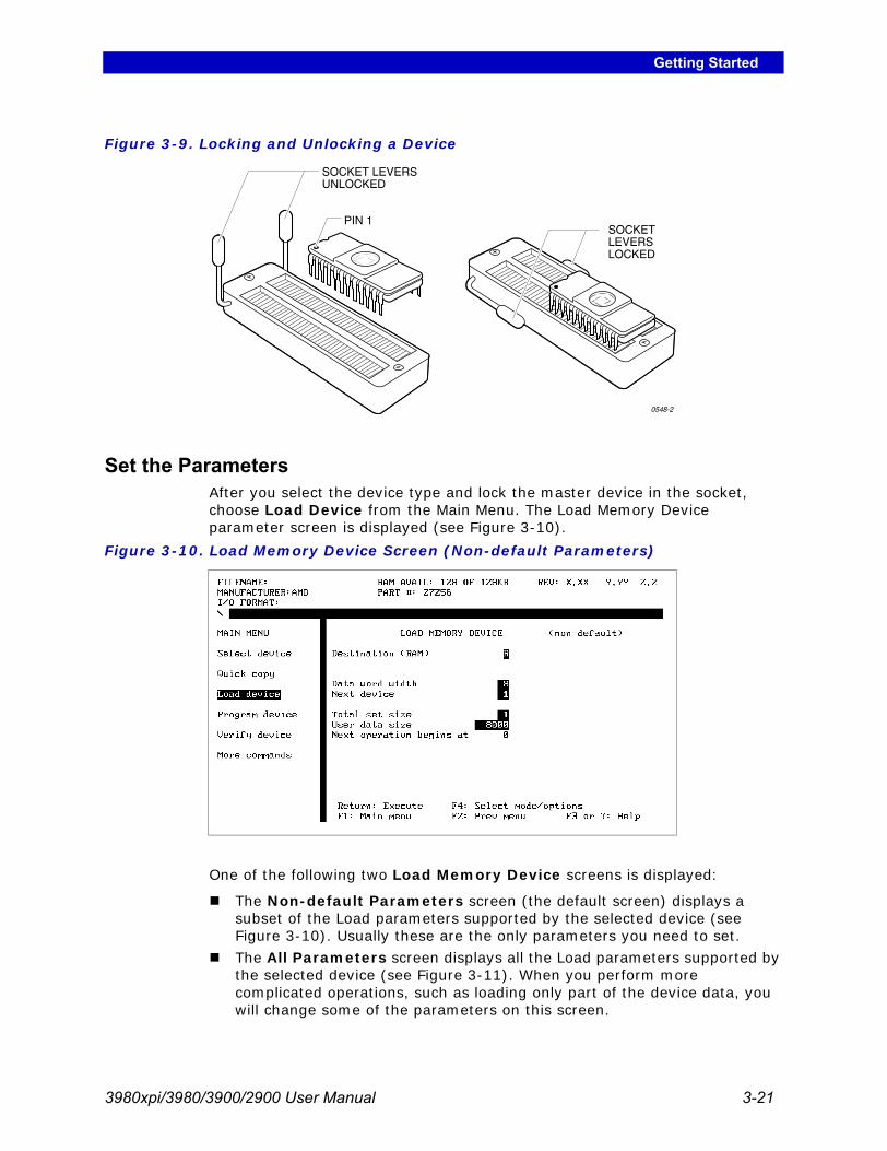
Getting Started
3980xpi/3980/3900/2900 User Manual 3-21
Set the ParametersAfter you select the device type and lock the master device in the socket, choose Load Device from the Main Menu. The Load Memory Device parameter screen is displayed (see Figure 3-10).
One of the following two Load Memory Device screens is displayed:
The Non-default Parameters screen (the default screen) displays a subset of the Load parameters supported by the selected device (see Figure 3-10). Usually these are the only parameters you need to set. The All Parameters screen displays all the Load parameters supported by the selected device (see Figure 3-11). When you perform more complicated operations, such as loading only part of the device data, you will change some of the parameters on this screen.
Figure 3-9. Locking and Unlocking a Device
Figure 3-10. Load Memory Device Screen (Non-default Parameters)
0548-2
SOCKET LEVERSUNLOCKED
PIN 1SOCKETLEVERSLOCKED

Getting Started
3-22 3980xpi/3980/3900/2900 User Manual
To switch between the two screens, press F4. For this Session you will be using the Non-default screen.
Set the parameters as shown in Figure 3-10. To change the value of a parameter, move the cursor to the desired field, type the new value, then either press ENTER or use the arrow keys to move the cursor to a new field.
If you try to enter an incorrect parameter, the programmer beeps and the message line reads Illegal parameter value. If you enter a valid parameter, the message line reads Parameter Entered.
For more information on a parameter, see Chapter 4 or use online Help.
Load the DataNow that you have set the parameters, you can load the data from the device.
To begin the load, press ENTER. When the programmer has loaded the data, it displays: OPERATION COMPLETE: Sumcheck = xxxxxxxx, where xxxxxxxx represents the 8-digit sumcheck of the data loaded from the device. (A 4-digit sumcheck is displayed for a logic device.)
ReviewWhen you select Load Device from the Main Menu, you see either the Non-default screen or the All Parameters screen. Press F4 to toggle between the two. Set the parameters, then press ENTER to begin the Load operation. When the programmer is finished loading the data from the device, it displays the sumcheck.
Figure 3-11. Load Memory Screen (All Parameters)

Getting Started
3980xpi/3980/3900/2900 User Manual 3-23
Session 6: Loading Data from a DiskThis Session describes how to load binary device data into the programmer from the programmer's floppy disk drive. You can use the sample data file (sample.bin) included on the Boot files/System files disk for this Session. Before starting this Session, complete Session 2 and be familiar with the programmer's user interface.
Use the Load File command when the data file to be loaded contains a binary image of the data you want to program into a device. The Save File command creates a binary image file by copying the data in the programmer's RAM directly to a disk file. The Load File command loads the binary data file directly into memory.
Note: The Transfer Data command transfers formatted data files between either the programmer and another machine (like a PC) or programmer RAM and the programmer disk drive.
Note: Do not use the Load File and Save File commands with formatted data files. Use the Input from Disk and Output to Disk commands to load and save formatted data files.
1.Select File Operations from the More Commands menu. The File menu is displayed (see Figure 3-12).
2.Place the Utility disk in the programmer drive. 3.Select the View Directory command and locate the sample.bin file on the
Utility disk. The programmer displays only 28 files at one time. Press CTRL+N to see the next page of files.
4.Select sample.bin, then press F2 to return to the File menu.
Figure 3-12. File Menu

Getting Started
3-24 3980xpi/3980/3900/2900 User Manual
5.Select Load File from the File menu. The dialog window displays a directory of the files on the disk. A screen similar to what you will see is shown in Figure 3-13.
Note: The Load File command loads a RAM Image Binary file from disk into RAM. Do not use this command to load files from a PC or from a file server.
6.Move the cursor to the Filename field, type sample.bin, then press ENTER. The programmer displays Parameter Entered.
7.Move the cursor to the Memory Begin Address field and type 0.8.Press ENTER to begin loading the data file. The action symbol rotates while
the programmer loads the data file, and displays: Loading data from file.
9.If the data file loads successfully, the programmer displays Done and the Load File screen is displayed. Go to page 3-31 to learn how to edit the sample file.
If the sample data file did not load successfully, return to the beginning of this Session and try it again.
ReviewYou can load device data into programmer RAM by loading a data file from the programmer's floppy disk drive. Use the commands on the File Operations menu (such as the Load File command) if your data file is stored in binary image format. Use the commands on the Transfer Data menu (such as the Input from Disk command) if your data file is stored in a specific data translation format, such as Intel Hex or JEDEC.When you select the Load File command, the programmer displays a directory of the files on the disk in the drive. Enter the filename of the file you want to load. Press CTRL+N to display the next page of files; press CTRL+P to display the previous page. When loading data for a memory device, also enter a memory begin address.Press ENTER to begin loading. If the load operation completes successfully, the programmer displays the following message in the message bar: Done.
Figure 3-13. Load File Dialog Screen
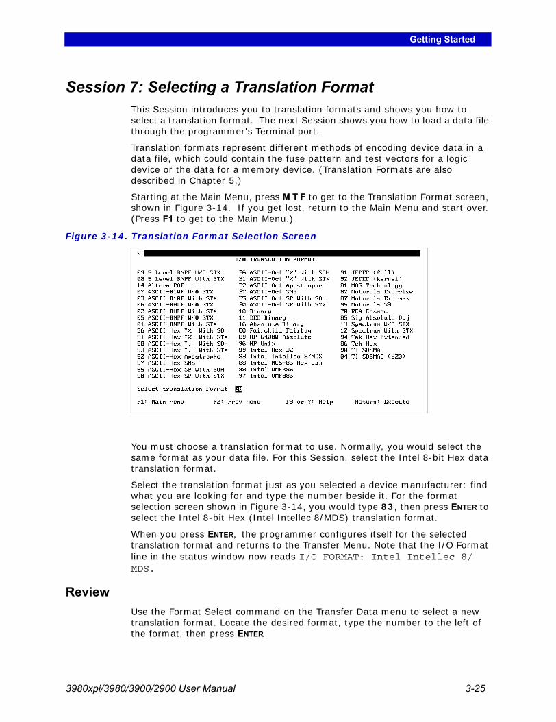
Getting Started
3980xpi/3980/3900/2900 User Manual 3-25
Session 7: Selecting a Translation FormatThis Session introduces you to translation formats and shows you how to select a translation format. The next Session shows you how to load a data file through the programmer's Terminal port.
Translation formats represent different methods of encoding device data in a data file, which could contain the fuse pattern and test vectors for a logic device or the data for a memory device. (Translation Formats are also described in Chapter 5.)
Starting at the Main Menu, press M T F to get to the Translation Format screen, shown in Figure 3-14. If you get lost, return to the Main Menu and start over. (Press F1 to get to the Main Menu.)
You must choose a translation format to use. Normally, you would select the same format as your data file. For this Session, select the Intel 8-bit Hex data translation format.
Select the translation format just as you selected a device manufacturer: find what you are looking for and type the number beside it. For the format selection screen shown in Figure 3-14, you would type 83, then press ENTER to select the Intel 8-bit Hex (Intel Intellec 8/MDS) translation format.
When you press ENTER, the programmer configures itself for the selected translation format and returns to the Transfer Menu. Note that the I/O Format line in the status window now reads I/O FORMAT: Intel Intellec 8/MDS.
ReviewUse the Format Select command on the Transfer Data menu to select a new translation format. Locate the desired format, type the number to the left of the format, then press ENTER.
Figure 3-14. Translation Format Selection Screen
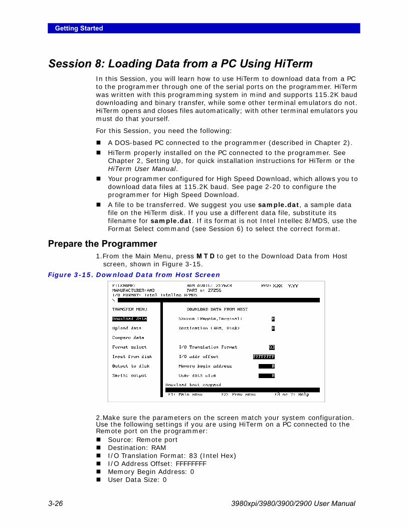
Getting Started
3-26 3980xpi/3980/3900/2900 User Manual
Session 8: Loading Data from a PC Using HiTermIn this Session, you will learn how to use HiTerm to download data from a PC to the programmer through one of the serial ports on the programmer. HiTerm was written with this programming system in mind and supports 115.2K baud downloading and binary transfer, while some other terminal emulators do not. HiTerm opens and closes files automatically; with other terminal emulators you must do that yourself.
For this Session, you need the following:
A DOS-based PC connected to the programmer (described in Chapter 2).HiTerm properly installed on the PC connected to the programmer. See Chapter 2, Setting Up, for quick installation instructions for HiTerm or the HiTerm User Manual. Your programmer configured for High Speed Download, which allows you to download data files at 115.2K baud. See page 2-20 to configure the programmer for High Speed Download.A file to be transferred. We suggest you use sample.dat, a sample data file on the HiTerm disk. If you use a different data file, substitute its filename for sample.dat. If its format is not Intel Intellec 8/MDS, use the Format Select command (see Session 6) to select the correct format.
Prepare the Programmer1.From the Main Menu, press M T D to get to the Download Data from Host
screen, shown in Figure 3-15.
2.Make sure the parameters on the screen match your system configuration. Use the following settings if you are using HiTerm on a PC connected to the Remote port on the programmer:
Source: Remote portDestination: RAMI/O Translation Format: 83 (Intel Hex)I/O Address Offset: FFFFFFFFMemory Begin Address: 0User Data Size: 0
Figure 3-15. Download Data from Host Screen

Getting Started
3980xpi/3980/3900/2900 User Manual 3-27
3.For now, leave the Download Host Command blank. If the other parameters are correct, go to “Download the File.”
Note: To find out more about the parameters, see Chapter 4.
To change a parameter, move the cursor to the field you want to change, type the new value, then move the cursor to another field. If the parameter is acceptable, Parameter Entered is displayed. If you enter an incorrect parameter, the programmer beeps and displays an error message. Continue until the displayed parameters match your configuration.
Download the File1.Change to the directory that contains the data file you will download, such as
sample.dat. In DOS, use the CD and DIR commands. In HiTerm, press ALT+F6 ENTER to view the current directory. If sample.dat is in the current directory, press ENTER to return to terminal emulation. If sample.dat is not in the current directory, press ALT+F5 to display HiTerm's Change Directory command. Type the drive and path name of the directory containing sample.dat, then press ENTER to change to that directory. Press ALT+F6 ENTER to view the current directory. If sample.dat is in the current directory, press ENTER to return to terminal emulation. If the data file is not in the current directory, repeat the procedure until you find the desired data file.Note: The function key commands in this Session are for IBM-compatible PCs. If you are using an NEC-9800 PC, the HiTerm commands will be slightly different. See the HiTerm User Manual.
2.In the Download Host Command field, type tr sample.dat (or substitute the appropriate filename if you are using a different file). The TRANSFER (TR) command is a special Download Host Command that tells HiTerm and the programmer to perform a High Speed Download.
3.Press ENTER to begin the download. The message bar displays Parameter Entered and the action symbol rotates while the data is being downloaded.
4.When the download is finished, the message bar displays Data transfer complete. Data sum = xxxxxxxx, where xxxxxxxx indicates the sumcheck of the transferred data.
You can use the sumcheck to verify that the downloaded data matches the data on your host. The sumcheck for memory devices is an eight-digit hexadecimal summation of the data downloaded. When you program this data into a device, the programmer generates another sumcheck. If the two sumchecks match, the programmed data and downloaded data match.
ReviewIn this Session, you learned how to download data to the programmer from a host connected to the programmer's Terminal port. The steps are:1.Select the translation format that matched the format of your data file.
2.Press M T D TO Go to the download screen. 3.Set the parameters on the Download screen to match your setup. 4.Enter the host Download Host Command. For example, on a PC using
HiTerm, to transfer file filename.dat type tr filename.dat.

Getting Started
3-28 3980xpi/3980/3900/2900 User Manual
Session 9: Loading Data from a HostIn this Session, you will learn how to download data from a host to the programmer through one of the serial ports on the programmer. The procedures in this Session apply to many types of hosts, including VAXes, UNIX-based workstations, and DOS-based PCs.
Note: If you are using a DOS-based PC, we recommend that you use HiTerm as your terminal emulation software. Downloading a file with HiTerm is covered in the previous Session.
This Session assumes that you have a host connected to one of the serial ports on the programmer and a terminal connected to the other serial port on the programmer. This type of configuration is called Transparent mode.
See Chapter 2, Setting Up, for information on connecting a host and terminal to the programmer.
About Transparent ModeTransparent mode allows the programmer to be connected inline between your terminal and host computer, eliminating the need for a switch box or a second link to the host and enabling you to download directly from the host to the programmer. The host could be a networked file server, such as a VAX or a Sun. When set up properly, the terminal connected to the programmer can control both the programmer and the remote host.
In Transparent mode, the programmer passes all characters through its Terminal and Remote ports as if it weren't there. The two serial ports on the programmer can even operate at different baud rates. While operating the programmer from the terminal, press ESC CTRL+T to toggle the programmer between terminal mode and transparent mode. The programmer remains in transparent mode until it receives another ESC CTRL+T = command, which switches it back to terminal mode.
Preparing the FileUsing your development tools, create a small sample data file. For the rest of this Session, the sample data file will be referred to as sample.dat. If you give your sample data file a different name, substitute that name where you see sample.dat.
Also, the rest of this Session assumes that your sample data file is stored in the Intel Intellec 8/MDS data translation format. If your data file is in a different translation format, use the Format Select command to select that format. See Session 7 for information on selecting a data translation format.
Terminal/Workstation
HostT R
0544-2
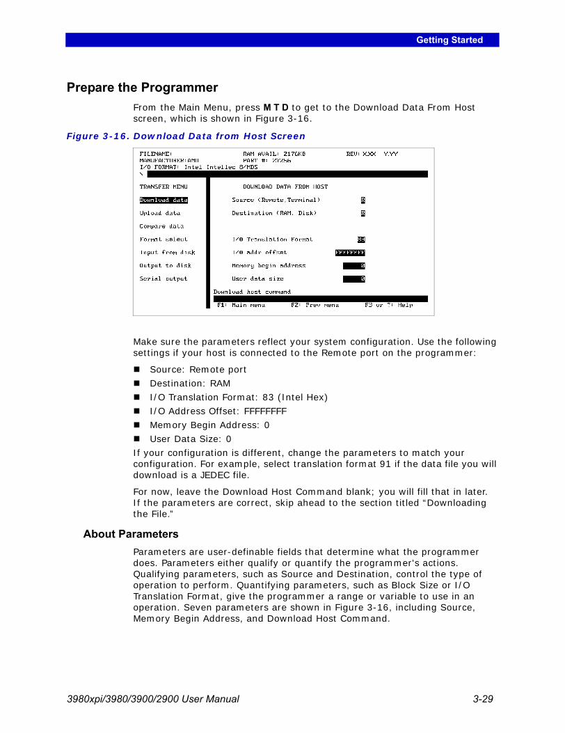
Getting Started
3980xpi/3980/3900/2900 User Manual 3-29
Prepare the ProgrammerFrom the Main Menu, press M T D to get to the Download Data From Host screen, which is shown in Figure 3-16.
Make sure the parameters reflect your system configuration. Use the following settings if your host is connected to the Remote port on the programmer:
Source: Remote portDestination: RAMI/O Translation Format: 83 (Intel Hex)I/O Address Offset: FFFFFFFFMemory Begin Address: 0User Data Size: 0
If your configuration is different, change the parameters to match your configuration. For example, select translation format 91 if the data file you will download is a JEDEC file.
For now, leave the Download Host Command blank; you will fill that in later. If the parameters are correct, skip ahead to the section titled “Downloading the File.”
About ParametersParameters are user-definable fields that determine what the programmer does. Parameters either qualify or quantify the programmer's actions. Qualifying parameters, such as Source and Destination, control the type of operation to perform. Quantifying parameters, such as Block Size or I/O Translation Format, give the programmer a range or variable to use in an operation. Seven parameters are shown in Figure 3-16, including Source, Memory Begin Address, and Download Host Command.
Figure 3-16. Download Data from Host Screen

Getting Started
3-30 3980xpi/3980/3900/2900 User Manual
Follow the steps below if you need to change a parameter:
1.Move the cursor to the field you need to change.
2.Type the new value and move the cursor to another field. If the parameter is acceptable, the programmer displays Parameter Entered in the message bar, which is located below the status window.
If you enter an incorrect parameter, the programmer beeps and displays an error message. Continue until the displayed parameters match your configuration.
Download the File1.Press ESC CTRL+T to enter Transparent mode.
2.Change to the directory containing the file you will download (for a UNIX-based host, use the CD command).
Note: The commands in this Session are for UNIX-based hosts. Substitute the appropriate commands if you are using a different host, such as a VMS-based machine. If you need more information, consult the system's documentation or your system administrator.
3.Press ESC CTRL+T to leave Transparent mode and return to the programmer interface. (You may have to press CTRL+R to redraw the screen.)
4.If the sample data file is in your current directory, type the following Download Host Command: cat sample.dat (substitute the appropriate filename if you are using a different file), then press ENTER. The message bar displays Parameter Entered.
The Download Host Command is a command that the programmer sends to the host to initiate the download. Because you are on a UNIX-based host, you use the CAT command as the Download Host Command.
5.Press ENTER to begin the download. The action symbol rotates while the data is being downloaded. When the download is finished, the message bar displays Data transfer complete. Data sum = xxxxxxxx, where xxxxxxxx indicates the sumcheck of the data transferred.
The sumcheck for memory devices is an eight-digit hexadecimal summation of the downloaded data. If you change one byte of information in the data file, the sumcheck will also change. The sumcheck is a good method of verifying that the data you downloaded matches the data on your host.Later, when you program this data into a device, the programmer will generate another sumcheck. If the two match, the data programmed is the same as the data downloaded. If the two sumchecks are different, the data programmed is not the same as the data downloaded.
ReviewIn this Session, you learned how to download data to the programmer from a host connected to the Remote port on the programmer. The steps were
1.Select the translation format that matched the format of your data file.
2.From the Main Menu, press M T D to go to the download screen. 3.Set the parameters on the Download screen to match your setup. 4.Enter the host Download Host Command. For example, to transfer the file
filename.dat you would enter cat filename.dat for a UNIX-based host. If you are using a VMS-based host, you would enter type filename.dat.

Getting Started
3980xpi/3980/3900/2900 User Manual 3-31
Session 10: Editing DataIn the previous Session, you loaded a data file into the programmer. In this Session, you will learn how to edit that data file.
1.Return to the Main Menu and select a memory device. (See Session 3.)
2.Select More Commands/Edit Data from the Main Menu, then select Edit Memory to display the Edit Programmer Memory screen (see Figure 3-17).
3.Set the parameters as shown in Figure 3-17, then press ENTER. The Edit screen is displayed (see Figure 3-18).
The edit screen displays 256 bytes at a time. The reminder bar at the bottom of the screen displays the available commands (no online Help is available for this screen), the right side of the screen displays the ASCII translation of the hexadecimal bytes on the left portion of the screen, and the top line of the screen displays the address location of the cursor (in hexadecimal) and the addressing mode.
Figure 3-17. Edit Programmer Memory Screen
Figure 3-18. Edit Screen

Getting Started
3-32 3980xpi/3980/3900/2900 User Manual
4.Read the message in the sample data file. As you can see there are some errors that need correcting.
5.The cursor starts in the upper-left corner of the hex display. Move the cursor around and watch the counter change to reflect your current location.
6.Press TAB to move the cursor to the ASCII side of the screen. (To edit hex data, you would move to the hex column.)
7.With the cursor in the ASCII field, move the cursor to the second r in prrgramming. Type o to correct the spelling.
8.Move the cursor to date and change it to read data.The previous two corrections were done in overtype mode: the typed characters replaced the previous characters. The next correction will be done in insert mode.
9.Turn on insert mode by pressing CTRL+T. The insert indicator is displayed on the bottom of the screen, indicating that every character you type will be inserted at the cursor and will push all following characters to the right.
10.Move the cursor on top of the period below the word loaded, and type the 3900.
11.If you are satisfied with your edits, press F2 to save them and return to the previous menu.If you are not satisfied with your edits and want to restore the current screen, press CTRL+U. The programmer restores the current screen of data to the state it was in after the last save.
Note: When you exit the Edit screen or move to another block, all edits are saved. When you save the edited file to RAM, there is no way to recall the original data file.
ReviewIn this Session, you learned how to edit a data file stored in RAM.
To access the programmer's built-in editor, press M E E from the Main Menu. Then, from the Edit Programmer Memory screen, select R to edit RAM. Once you are in the editor, you can edit data in either its hex representation or its ASCII representation. Press TAB to toggle between the two modes.
The editor defaults to overtype mode, but it can also operate in insert mode. Press CTRL+T to toggle between the two modes.
After editing a page of data, you can restore the page to its original condition by pressing CTRL+U.

Getting Started
3980xpi/3980/3900/2900 User Manual 3-33
Session 11: Programming a Memory DeviceThis Session shows you how to use the programmer to program a memory device. Before you go through this Session, complete Session 2.If you do not have an AMD 27256 (the device we are going to use for this Session), go to the Select Device screen and select the device you are going to program. The device you select might not have the same capabilities as the AMD 27256. For example, the AMD 27256 supports Electronic ID while the Hitachi 27256 does not.
Load the Data FileBefore you can program the device, you must perform the following steps to load your data into RAM.1.Create a binary file on a disk.
2.Insert the disk into the programmer disk drive.3.From the More Commands/File Operations menu, select the Load File
command to load the data file into RAM. This operation is described in detail in Session 6.
Set the ParametersAfter the data is loaded in RAM, select Program Device from the Main Menu. The Program Memory Device screen is displayed (see Figure 3-19).
One of the following two Program Memory Device screens is displayed:The Non-default Parameters screen (the default screen) displays a subset of the Program Memory Device parameters supported by the selected device (see Figure 3-19). Usually these are the only parameters you need to set. The All Parameters screen displays all the Program Memory Device parameters supported by the selected device (see Figure 3-20). When you perform more complicated operations, such as programming only part of the device, you will change some of the parameters on this screen.
Figure 3-19. Program Memory Device Screen (Non-default Parameters)

Getting Started
3-34 3980xpi/3980/3900/2900 User Manual
To switch between the two screens, press F4. For this Session you will be using the Non-default screen.
During normal programming, you usually need only the parameters on the Non-default screen. But if you want to do some more complicated programming operations, you need to change some of the parameters on the All Parameters screen. An example of a complicated programming operation would be if you wanted to program only part of a device.
For this Session, you should be looking at the Non-default screen. If the All Parameters screen is displayed, press F4 to switch to the Non-default screen.
Program the DeviceFor this Session, you do not need to set any programming parameters, so you are ready to program the data file into the device. To begin programming, press ENTER. After the programmer has programmed the device, the following message is displayed in the message bar: OPERATION COMPLETE: Sumcheck = xxxxxxxx, where xxxxxxxx represents is the 8-digit (4-digit for a logic device) sumcheck of the data programmed into the device in the socket.
ReviewWhen you select Program Device from the Main Menu, either the Non-default Parameters screen or the All Parameters screen. Press F4 to toggle between the two parameter screens.
Enter the programming parameters, then press ENTER to begin programming.
When the programmer is finished programming, it displays the sumcheck.
Figure 3-20. Program Memory Device Screen (All Parameters)

Getting Started
3980xpi/3980/3900/2900 User Manual 3-35
Session 12: Verifying a DeviceOnce you have programmed a device, you can perform a number of different device checks and programming tests on the device. For the rest of this Session we will refer to device checks and programming tests as verify operations.
Note: During this Session, you will verify a device with data stored in RAM.
Make sure you have completed Session 2, which is an introduction to the programmer's interface. Also make sure you have completed Session 11, which covers programming a device.
If you do not have an AMD 27256 (the device we are going to use for this Session), then go to the Select Device screen and select the device you are going to program. Keep in mind that the device you select might not have the same capabilities as the AMD 27256. For example, the AMD 27256 supports Electronic ID while the Hitachi 27256 does not.
Set the ParametersSelect Verify Device from the Main Menu. The dialog window displays the Verify Memory Device screen (see Figure 3-21).
One of the following two Verify Memory Device screens is displayed:
The Non-default Parameters screen (the default screen) displays a subset of the Verify Memory Device parameters supported by the selected device (see Figure 3-21). Usually these are the only parameters you need to set. The All Parameters screen displays all the Verify Memory Device parameters supported by the selected device (see Figure 3-22). When you perform more complicated operations, such as verifying only part of the device, you will change some of the parameters on this screen.
Figure 3-21. Verify Memory Device Screen (Non-default Parameters)

Getting Started
3-36 3980xpi/3980/3900/2900 User Manual
To switch between the two screens, press F4. For this Session you will be using the Non-default screen.
If you just completed Session 11, Program a Memory Device, you probably do not need to set any parameters. Your parameters should match those in Figure 3-21.
User data size defaults to the size of the selected device, but if you already performed an operation on the device (as you did in this Session), the programmer sets this value (along with Block Size and Begin Address) to the parameters specified in the previous device operation.
Note: Remember that the displays may look different if you are using a device other than an AMD 27256.
Verify the DeviceYou are ready to verify the data programmed into the device.
To begin the verify, press ENTER. If the verify operation completes successfully, the following message is displayed in the message bar: OPERATION COMPLETE: Sumcheck = xxxxxxxx, where xxxxxxxx represents is the 8-digit (4-digit for a logic device) sumcheck of the data in the device.
ReviewWhen you select Verify Device from the Main Menu, you see either the Non-default screen or the All Parameters screen. Press F4 to toggle between the two parameter-entry screens.
After you enter the Verify parameters, press ENTER to begin the verify operation.
When the programmer is finished verifying, it displays the sumcheck of the data in the device.
Figure 3-22. Verify Memory Device Screen (All Parameters)

3980xpi/3980/3900/2900 User Manual 4-1
4 Commands
This chapter describes the commands accessible from the programmer's terminal menus. The menu and command structure is shown in the Command Tree on page 4-2. Each command description includes the path to that command.
Note: For Tasklink for Windows and for DOS, please see online help.
The commands are described on the following pages. (The Command Tree also shows page numbers):
Overwriting User RAM . . . . . . . . . . . . . . . . . . . . . . . . . . . . . . . . . . . . . 4-1Factory Default Settings . . . . . . . . . . . . . . . . . . . . . . . . . . . . . . . . . . . 4-3Select Device . . . . . . . . . . . . . . . . . . . . . . . . . . . . . . . . . . . . . . . . . . . 4-5
Cross Programming . . . . . . . . . . . . . . . . . . . . . . . . . . . . . . . . . . . . 4-6Quick Copy . . . . . . . . . . . . . . . . . . . . . . . . . . . . . . . . . . . . . . . . . . . . 4-7Load Device . . . . . . . . . . . . . . . . . . . . . . . . . . . . . . . . . . . . . . . . . . . . 4-8Program Device . . . . . . . . . . . . . . . . . . . . . . . . . . . . . . . . . . . . . . . . 4-10Verify Device . . . . . . . . . . . . . . . . . . . . . . . . . . . . . . . . . . . . . . . . . . 4-15More Commands. . . . . . . . . . . . . . . . . . . . . . . . . . . . . . . . . . . . . . . . 4-18
Configure System . . . . . . . . . . . . . . . . . . . . . . . . . . . . . . . . . . . . 4-19Device Checks . . . . . . . . . . . . . . . . . . . . . . . . . . . . . . . . . . . . . . . 4-39Edit Data . . . . . . . . . . . . . . . . . . . . . . . . . . . . . . . . . . . . . . . . . . 4-45File Operations . . . . . . . . . . . . . . . . . . . . . . . . . . . . . . . . . . . . . . 4-53Job File. . . . . . . . . . . . . . . . . . . . . . . . . . . . . . . . . . . . . . . . . . . . 4-58Remote Control . . . . . . . . . . . . . . . . . . . . . . . . . . . . . . . . . . . . . . 4-59Self-Test . . . . . . . . . . . . . . . . . . . . . . . . . . . . . . . . . . . . . . . . . . . 4-60Transfer Data . . . . . . . . . . . . . . . . . . . . . . . . . . . . . . . . . . . . . . . 4-61Yield Tally . . . . . . . . . . . . . . . . . . . . . . . . . . . . . . . . . . . . . . . . . . 4-69
Overwriting User RAMThe following operations use User RAM as a temporary storage buffer and overwrite existing data.
Duplicate DiskCopy FileSerial Output from Disk FileDownload Data to Disk FileSelf-test User RAMUpload Data from Disk FileOutput Data to Disk from Disk FileInput Data from Disk to Disk FileCompare Data to Disk FileCreate and Add Custom Menu Algorithms

Commands
4-2 3980xpi/3980/3900/2900 User Manual
Figure 4-1. Command Tree (page numbers are in italics)
ConfigureSystem
RemoteControl
FileOperations
DeviceChecks
Edit Data
Job File
Self-test
Yield Tally
TransferData
Logic Memory
QuickCopy
ProgramDevice
MoreCommands
VerifyDevice
LoadDevice
0542-8
Restore
Edit Parameters
Save
Terminal Type
Programmer ID
Sumcheck Display
Compare Elec. ID
Illegal Bit Check
Blank Check
Electronic Erase
Edit Logic
Vector Edit
Fill Fuse Map
Clear Vectors
View Directory
Load File
Save File
Purge File
Rename File
Copy File
Duplicate Disk
Format Disk
Download Data
Upload Data
Compare Data
Format Select
Input From Disk
Output To Disk
Serial Output
Programming
Serial I/O
Communication
Interface
Edit Memory
Complement
Data Copy
Fill Memory
Part Number List
Keep Current
Replace/Restore
Manufact. List
Under/Overblow
View
Delete
Purge
Swap Data
Custom Menu Algs.
Add
Create
View
Delete
SelectDevice
Update
Mass Storage
Device Configure
Keep Current Part Number
4-7
4-10
4-18
4-15
4-8
4-5
4-19
4-59
4-53
4-39
4-45
4-58
4-60
4-69
4-61
4-19
4-20
4-31
4-31
4-39
4-41
4-41
4-42
4-32
4-38
4-34
4-32
4-42
4-43
4-44
4-33
4-34
4-35
4-36
4-37
4-37
4-38
4-32
4-32
4-26
4-30
4-21
4-25
4-45
4-46
4-48
4-48
4-49
4-51
4-52
4-52
4-524-53
4-53
4-54
4-55
4-55
4-56
4-56
4-57
4-61
4-62
4-64
4-65
4 -65
4-66
4-67

Commands
3980xpi/3980/3900/2900 User Manual 4-3
Factory Default SettingsThe programmer's system parameters are initialized at the factory. To restore these factory defaults at any time, go to the More Commands/ Configure System/Restore System Parameters menu, type 0, then press ENTER.
The powerup defaults (configuration file number 1) match the factory defaults (configuration file number 0) when the unit is shipped from Data I/O.
Parameter Factory Default Setting
Abort on Empty Socket YesAlgorithm Type D Blank Check Yes Continuity Check Yes Compare Electronic ID Yes Data Source/destination RAM Data Word Width 8 Device Begin Address 0 Device Block Size 1000 Display Device Footnote YEnable Download Echo NoEnable Special Data NoEnable Terminal Beep YesEnable Yield Tally option No EE Bulk Erase option No EOF Delimiter Flag (download) NoEOF Delimiter Flag (upload) NoFile Delimiter Character (download) 1A (Ctrl+Z)File Delimiter Character (upload) 1A (Ctrl+Z)Filename Blank Fill RAM Before Downloading NoFill RAM with Data (00 to FF) 00 High-speed Logic Drivers Yes Host Command (Download) Blank Host Command (Upload) Blank Illegal Bit Check Yes Instrument Control Code (0,1,2) 0 I/O Address Offset FFFFFFFF I/O Translation Format 0 (no default) I/O Timeout 30 seconds JEDEC I/O Translate DIP/LCC option Yes Logic Verification (all, fuse, vector) All Main Menu Job Files NoManufacturer Blank (no default) Memory Begin Address 0 Number of lines between form feeds 0Number of nulls 0

Commands
4-4 3980xpi/3980/3900/2900 User Manual
* This parameter is not restored when the Restore Configuration operation is performed. It is, however, used at powerup if it is saved as a powerup parameter.
Odd/Even Byte Swap No Part Number (no default)Power On CRC Mode No Powerup User RAM Test YesProgram Security Fuse No RAM Device Selection NoReject option (commercial or single) Commercial Remote Off Code 0 Remote On Code 0 Remote Serial Port Configuration 9600 baud, 1 stop bit, 8 data bits,
no parity, active CTS/DTRSecurity Fuse Data (0 or 1) 0 Serial Set Auto Increment Flag No Simple/complex Parameter screen Simple Terminal Serial Port Configuration 9600 baud, 1 stop bit, 8 data bits,
no parity, active CTS/DTRTerminal Type VT-100 Transmit Pacing 0 User Menu Port * T User Data Size 0 Upload Wait 0 seconds Upload Destination/download Source Remote Upload Record Size 16 Verify Data Format Hex Verify Passes 2
Parameter Factory Default Setting

Commands
3980xpi/3980/3900/2900 User Manual 4-5
Select Device (Terminal Mode)Before you can perform any device-related operations with the programmer, you must select the device you are using.
Before You Select a Device Before you select a device, select the Algorithm Type that matches the device you want to use. (See “Algorithm Type” on page 4-21 for more information.)
1. From the Main Menu, select More commands/ Configure system/Edit/Programming. (Press F1 to return to the Main Menu from any submenu.)
2. Select one of the following algorithm types:
D (Default)Choose D if you will be selecting a device from the Manufacturer List, which contains almost all the devices supported by your programmer. E (Extended Algorithm)Choose E if you will be selecting a device from an Extended Algorithm list, which contains devices that use extended algorithms for programming. K (Keep Current)Choose K if you will be selecting a device from a Keep Current list, which contains devices that use Keep Current algorithms for programming (see “Keep Current” on page 4-32 for more information). (You can also access Keep Current devices by choosing D, then selecting KEEP CURRENT from the manufacturers list. C (Custom Menu)Choose C to select a device from a Custom Menu list, which contains devices you included in a Custom Menu (see “Custom Menu Algs” on page 4-34 for more information).
3. After you set the Algorithm Type, press F1 to return to the Main Menu.
Note:To save your Algorithm Type and other parameter changes as powerup defaults, see page 4-31.
Select a Device Main Menu / Select Device / Device List
1. From the Main Menu, choose Select Device. (Press F1 to return to the Main Menu if needed.)
2. If you are prompted to do so, insert the requested disk.
3. Depending on the Algorithm Type you selected, one of the following screens is displayed:
Device Manufacturer List screen (if you chose D).Extended Algorithm screen (if you chose E). Keep Current screen (if you chose K).Custom Menu screen (if you chose C).
Note: If the screen you want to view is not displayed, select the correct algorithm type as described above.

Commands
4-6 3980xpi/3980/3900/2900 User Manual
4. In the Manufacturer field, enter the number that is next to the item you want to select. For example, to select KEEP CURRENT, type 1 in the manufacturer field, then press ENTER. The upper-right corner of the screen displays the total number of screens (pages) and the page you are on. Press CTRL+N to go to the next page or CTRL+P to go to the previous page.When you select a manufacturer, you can set the device type filter to the appropriate setting for the device you are using. Logic Only displays only logic devices, Memory & Emicros displays memory and emicro devices, and All displays all device types. Press SPACE to cycle through the filter types. The list changes accordingly.
5. After you select the manufacturer, a list of devices is displayed. Find the device you want to use, then enter the number next to that device.If you do not see the device you are looking for, press CTRL+N to move to the next page or press CTRL+P to return to the previous page.
6. After you enter the correct number, press ENTER. The programmer returns to the Main Menu and the status window shows the device you selected.
Cross ProgrammingCross programming allows a single generic programmable logic device (PLD) to be configured as any one of many PLD architectures. Consequently, the generic device can take on the function of many subset devices. The term generic PLD is used to identify the superset device, such as a 16V8 generic PLD, which can be configured as a 16R4, 16R8, or a 16L8.
The generic PLD and the subset devices it can support are not restricted to the same manufacturer. For example, a 16V8 generic PLD from manufacturer A can be programmed using a fuse pattern originally designed for a 16L8 from manufacturer B. The cross-programming feature allows you to avoid recompiling source code for the generic PLD if the appropriate fuse pattern is available for a subset part.
Follow these steps to cross-program a device:
1. Select a manufacturer with an XPGM extension, then press ENTER. A list of all devices that can be replaced by the generic PLD of the selected manufacturer is displayed.
2. From the Part Menu for Manufacturer screen, select the appropriate device, such as 16V8 as 16L8 if a 16L8 fuse map has been loaded and a 16V8 generic PLD is to be programmed. Then press ENTER.
3. Load the fuse map of the subset PLD into User Memory by using either a Load From Device operation or a Download of a JEDEC file.
4. From the Main Menu, select the Program Devices screen. 16V8 as 16L8 will be displayed in the PART # field at the top of the screen.
5. Insert the 16V8 and press ENTER. The 16V8 is programmed as a 16L8.

Commands
3980xpi/3980/3900/2900 User Manual 4-7
After You Select a Device After you select a device, any online device-specific information for the selected device is displayed. If the information takes up more than one screen, press CTRL+N to view the next screen or CTRL+P to view the previous screen. To exit the screen, press F1 or F2. If the Display Device Footnotes parameter (in the More commands/Configure system/Edit/Programming screen) is set to N, no device-specific information is displayed. If there is online device-specific information for the selected device, Hit F3 or ? to view device specific message is displayed. To view the online information, press F3 or ?. The screen clears and the programmer displays the device-specific information.
Note: If only the footnote number appears in the message bar, make sure the correct disk is inserted into the programmer's drive. Footnote (device-specific) information is also included in the Device List.
The device manufacturer and part number appears in the status window and the programmer displays only screens related to the type of device you selected. For example, if you choose a logic device, you will see only screens that are required to load, program, edit, and verify a logic device.Also, some devices support special functions, such as the Program Signature and XNOR table. If the device you select supports a particular function, parameter entry fields associated with that function are displayed.
Quick CopyMain Menu / Quick Copy
The Quick Copy command allows you to load data from a master device and program that device data into a target device quickly and easily.
Note: The manufacturer and device name must be the same for both the master and the target devices. Before you use Quick Copy, you must first select a device.
To use the Quick Copy command, follow these steps:
1. Select the device containing the data you are going to load (see page 4-5).2. Select the Quick Copy command by pressing Q from the Main Menu. The
dialog window displays the Quick Copy screen. The message bar displays Insert master device. Hit return.
3. Insert the master device and lock it into place.4. Press ENTER to load the master data into RAM. When the data is loaded,
OPERATION COMPLETE: Sumcheck = xxxxxxxx Hit return appears.
5. Remove the master device, then press ENTER. The programmer displays Insert blank device. Hit return.
6. Insert the device to be programmed (target device) and lock it into place.7. Press ENTER to program the device.8. When the programming operation is complete, the programmer displays
OPERATION COMPLETE: Sumcheck = xxxxxxxx Hit return.
9. Remove the device. The Quick Copy operation is complete. 10. To program another device, return to step 6.

Commands
4-8 3980xpi/3980/3900/2900 User Manual
Load DeviceThe Load Device command allows you to copy data from a master device into RAM. Depending on whether you select a logic or memory device, either the Load Logic Device screen or the Load Memory Device screen will appear when you select this command.
Load Logic DeviceMain Menu / Load Device / Load Logic Parameters screen
To load user memory with data from a logic device, follow these steps:
1. Select and socket a logic device.2. Select Load Device from the Main Menu. The Load Logic Device screen is
displayed. 3. Press ENTER to begin the loading.4. When the load operation is complete, the programmer displays the
following message: OPERATION COMPLETE: Sumcheck = xxxx.
Load Memory DeviceMain Menu / Load Device / Load Memory Parameters screen
To load user memory with data from a memory device, follow these steps:
1. Select and socket a memory device.2. Select Load Device from the Main Menu. 3. From the Load Memory Device screen, specify the parameters you want,
then press ENTER to begin loading.4. When the load operation is complete, the programmer displays
OPERATION COMPLETE: Sumcheck = xxxxxxxx
You can specify the following parameters in the Load Memory Device screen:
Data Word WidthSets the word width of data to be loaded. For 8-bit or larger devices, the minimum word width equals the device width and the maximum word width is 64. For 4-bit devices, the word width choices are 4, 8, 16, and 32. This value should match the data bus word width in the target system for the device being programmed. The default value is the device word width.
Next DeviceDesignates the next device (next set member) in the set. For example, if you are using 8-bit devices and have specified a word width of 16 bits on the Load Memory Device screen, it requires two devices to store each 16-bit word. Type 1 for the next set member to direct the programmer to load the first device in the set at even-address bytes of the memory block. Type 2 to direct the programmer to load the second device at odd address bytes of the memory block.
Commands
3980xpi/3980/3900/2900 User Manual 4-9
Total Set SizeSpecifies the number of virtual devices in the set for device operations. For example, if you are loading 16-bit wide data from two 8-bit wide devices, your virtual device still equals one (one 16-bit virtual device). Enter any number from 1 to 99. Automatic Set Size calculation will be attempted when any of the following parameters are changed: Device Width, Data Word Width, Device Block Size or User Data Size. Total Set Size can be defined by the following equation:
User Data SizeSpecifies the hexadecimal size, in bytes, of the data block used to load from the device to the destination. This value is normally equal to the device size or to a multiple of the device size for loading a set. If 0 or a value less than the device size is entered, it is reset to the device size for the load. User Data Size works with Total Set Size to determine the total amount of bytes to load from a set of devices.
Next Operation Begins AtThis read-only parameter shows where in user memory the next data byte will be loaded. This value is calculated from the Data Word Width, Device Block Size, Memory Begin Address, device width, and next set member parameters.
Optional ParametersThe Non-default Parameters screen, which contains the preceding parameters and any default parameters that were changed, is displayed as the default. The more complex All Parameters screen displays the following additional parameters. To toggle between the two screens, press F4.
Memory Begin AddressSpecifies the beginning RAM address, in hex, where the first byte of data is loaded from a device. If you selected a 16-bit device, the Memory Begin Address must be an even address. The default address is 0.
Device Begin AddressSpecifies the first hex master device address that will be loaded. The default value is 0.
Device Block SizeSpecifies the size, in hex, of device data used in device operations. After you select a device, the Device Block Size is set automatically to the device size and normally does not need to be changed. Also, Device Block Size is set to a smaller value if the Device Begin Address is nonzero. This parameter can be changed if desired. Entering a zero sets the Device Block Size equal to the device size.
USER DATA SIZE
DATA WORD WIDTH
DEVICE WIDTHDEVICE BLOCK SIZE
=
0987-1
TOTAL SET SIZE

Commands
4-10 3980xpi/3980/3900/2900 User Manual
Set Auto-incrementThis option, used in serial set mode, directs the programmer to the next block in the set to be loaded. For example, if you have four 1K x 8 devices to load into a 4K x 8 block of memory, using the auto-increment option directs the programmer to the first memory address of the next 1K block after each device is loaded. For single device operations, disable this feature and set the Next Device parameter to 1. Note: Items with an * (asterisk) are visible on the screen only if the selected device supports the feature.
* Compare Electronic ID (Y,N)Compares the electronic ID of the socketed device against the electronic ID of the selected algorithm.
* Odd/Even Byte Swap (Y,N)When enabled, allows the Most Significant Bytes (MSB) and the least significant bytes (LSB) of 16-bit words to be swapped when data is loaded from a 16-bit device. When this parameter is disabled, the data from a 16-bit device is loaded into User RAM with the MSB stored at an odd memory address. When enabled, the MSB is stored at an even memory address.
Program DeviceThe Program Device command allows you to copy data from RAM. Depending on whether you select a logic or memory device, either the Program Logic Device screen or the Program Memory Device screen is displayed when you select this command. Before you can program a device, you must load the programming data into RAM, which is described on page 4-8.
Program Logic Device Main Menu/Program Device/Program Logic Parameters List
To program a logic device, follow these steps:1. Select and socket a logic device. 2. Select Program Device from the Main Menu. The Program Logic Device
screen is displayed.3. Specify the parameters you want, then press ENTER to begin programming.4. When programming is complete, the programmer displays the following
message: OPERATION COMPLETE: Sumcheck = xxxx.
The following parameters can be specified on the Program Logic Device screen.
Security Fuse Data (0,1)To program the security fuse, set this parameter to 1 and set the Program Security Fuse parameter to Y. This parameter defaults to 0, which disables programming of the security fuse.Program Security Fuse (Y,N)Enables or disables security fuse programming. To program the security fuse, select Y and set the Security Fuse Data parameter to 1. The default is N, which disables programming of the security fuse.
Commands
3980xpi/3980/3900/2900 User Manual 4-11
Optional ParametersThe Non-default Parameters screen, which contains the preceding parameters and any default parameters that were changed, is displayed as the default. The more complex All Parameters screen displays the following additional parameters. To toggle between the two screens, press F4.
Illegal Bit Check (Y,N)Enables (default) or disables the Illegal Bit test, which compares data in a device against data in programmer RAM to determine if the device has already-programmed locations of incorrect polarity. For example, the programmer would return an illegal-bit error if data in RAM indicates that a specific bit should be in an unprogrammed state but the corresponding bit in the device is in a programmed state.
The device cannot be programmed if the programmer detects an illegal bit.
Blank Check (Y,N)Enables (default) or disables the Blank Check test, which checks a device for programmed bits.
Enable Yield Tally (Y,N)When enabled, directs the programmer to keep a running tally of the programming yields for the last sixteen types of devices programmed. These totals show how many devices passed and failed, and what specific errors, if any, have occurred. The defaults is N. See “Yield Tally” on page 4-69 for more information.
Logic Verification (A,F,V)Specifies the type of logic verification to be performed after programming. Press SPACE to step through the following three choices:All (A)—Performs both fuse and vector verification. This is the default.Fuse Verification (F)—Checks the fuse pattern programmed into the device with the pattern in the programmer's memory. Vector Verification (V)—Tests the device using structured test vectors stored in memory. The programmer does not support vector testing for logic devices with more than 84 pins.
The programmer does not support vector testing for logic devices with more than 44 pins.—2900
Verify Passes (0,1,2)Selects the number of times to test the device.0—Do not to test the device.1—Test the device once at the device manufacturer's nominal Vcc. 2—Verify the device at the device manufacturer's recommended high and low Vcc levels. This is the default.
Reject Option (C,S)Selects the number of times the device is pulsed with programming voltage before it is rejected as unprogrammable. C—Selects the number of pulses specified by the manufacturer (the default). Unless you are programming devices to a strict military specification, leave this option set to C.S—Selects either one-pulse or military-specification number of pulses.

Commands
4-12 3980xpi/3980/3900/2900 User Manual
Program Memory Device Main Menu/Program Device/Program Memory Device Parameters
To program a memory device, follow these steps:1. Select and socket a memory device. 2. Select Program Device from the Main Menu. The Program Memory Device
screen is displayed.3. Specify the parameters you want. Then press ENTER to begin programming.4. When the programming is complete, the programmer displays the
following message: OPERATION COMPLETE: Sumcheck = xxxxxxxx
The following parameters are available.
Data Word WidthSets the word width of the data to be programmed. For 8-bit (or larger) devices, the minimum word width is equal to the device width and the maximum is 64. For 4-bit devices, your word width choices are 4, 8, 16, and 32. This value should match the data bus word width in the target system for the device being programmed.
Next DeviceDesignates the next device in the set. For example, if you are using 8-bit devices and have specified a word width of 16 bits on the Program memory device screen, it requires two devices to store each 16-bit word. 1 directs the programmer to program the first device in the set with even-numbered addresses of the memory block. 2 directs the programmer to use odd-numbered addresses.
Total Set SizeSpecifies how many virtual devices are in the set for device operations. For example, if you are programming 16-bit wide data into two 8-bit wide devices, your virtual device still equals one (one 16-bit virtual device). You can enter any number between 1 and 99. Automatic Set Size calculation is attempted when you change any of the following parameters: Device width, Device Block Size or User Data Size. Total Set Size is defined by the following equation:
User Data SizeSpecifies the hexadecimal size, in bytes, of the data block to program into a device. Normally, this value is equal to the device size or to a multiple of the device size for set programming. Entering 0 sets the User Data Size to the device size. User Data Size works with Total Set Size to determine the total amount of bytes to program into a set of devices.
Next Operation Begins AtThis read-only parameter shows what address in user memory contains the next data byte to be programmed. This value is calculated from the Data Word Width, Device Block Size, Memory Begin Address, device width, and next set member parameters. Note: Items with an * (asterisk) are visible on the screen only if the selected device supports the feature.
USER DATA SIZE
DATA WORD WIDTH
DEVICE WIDTHDEVICE BLOCK SIZE
=
0987-1
TOTAL SET SIZE

Commands
3980xpi/3980/3900/2900 User Manual 4-13
* Program Security Fuse (Y,N)Enables or disables the programming of the security fuse(s). To program the security fuse(s), set this parameter to Y and set the Security Fuse Data parameter(s) to 1. This parameter defaults to N, which disables programming of the security fuse(s).
* Program SignatureAvailable on only a few devices, the program signature is a user-definable field that allows the user to program data into the program signature array.
* Software Data Protection (Y,N)When enabled, prevents writing to a device.
Optional ParametersThe Non-default Parameters screen, which contains the preceding parameters and any default parameters that were changed, is displayed as the default. The more complex All Parameters screen displays the following additional parameters. To toggle between the two screens, press F4.
Memory Begin AddressSpecifies the beginning RAM address, in hex, of the first byte of data to be programmed. The Memory Begin Address must be an even address if you have selected a 16-bit device. The default address is 0.
Device Begin AddressSpecifies the first hex device address to be programmed. The default is 0.
Device Block SizeSpecifies the size in hex of device data used in device operations. At device selection, Device Block Size is automatically set to the device size and usually does not need to be changed. It is also set to a smaller value if the Device Begin Address is not zero. You can change this parameter. Entering zero sets the Device Block Size equal to the device size.
Set Auto-incrementWhen enabled, directs the programmer (in serial set programming mode) to the starting memory address of the next block in the set to be programmed.
For example, if you have four 1K x 8 devices to program from a 4K x 8 block of data, using the auto-increment option directs the programmer to point to the first address of the next 1K block after each device has been programmed. For single device operations, this feature should be disabled and the Next Device parameter should be set to 1. Note: Items with an * (asterisk) are visible on the screen only if the selected device supports the feature.
* Illegal Bit Check (Y,N)Enables or disables the illegal-bit test. This test compares data in a device against data in the programmer's RAM to determine if the device has already-programmed locations of incorrect polarity.
For example, the programmer returns an illegal-bit error in the following situation: data in RAM indicates a specific bit should be in an unprogrammed state while the corresponding bit in the device is in a programmed state. The device cannot be programmed if the programmer detects an illegal bit. This parameter is enabled by default.

Commands
4-14 3980xpi/3980/3900/2900 User Manual
Blank Check (Y,N)Enables or disables the Blank Check test, which checks a device for programmed bits. This parameter defaults to Y, which enables the test.
* Compare Electronic ID (Y,N)When enabled, compares the electronic signature of the device against the electronic signature of the selected algorithm. Enable Yield Tally (Y,N)When enabled, directs the programmer to keep a running tally of the programming yields for the last sixteen types of devices programmed. These totals show how many devices passed and failed, and what specific errors, if any, occurred. This parameter defaults to N. For more information, see “Yield Tally” on page 4-69.
* Odd/Even Byte Swap (Y,N)When enabled, allows the Most Significant Bytes (MSB) and the Least Significant Bytes (LSB) of 16-bit words to be swapped when data is programmed into a 16-bit device. The data is programmed into a device retrieving the Most Significant byte from an odd memory address when the flag is N and an even memory address when it is Y. Reject Option (C,S)Selects the number of times the device is pulsed with programming voltage before it is rejected as unprogrammable. C selects the number of pulses specified by the manufacturer. S selects either a one-pulse or the military-specification number of programming pulses. Unless you are programming devices to a strict military specification, you should leave this option set at C. This option defaults to C. Verify Passes (0,1,2)Selects the number of times to test the device. 0 directs the programmer not to test the device. 1 directs the programmer to test the device once at the device manufacturer's nominal Vcc. 2 directs the programmer to verify the device at the device manufacturer's recommended high and low Vcc levels. This parameter defaults to 2.
* Erase EE Device (Y,N)Allows you to erase electronically-erasable PROMs. Before the programming cycle, the programmer checks the device and displays a warning if the device if non-blank. If you enable the erasing of the device, the programmer erases the device before programming the device.
Enhanced Security Fuse CapabilityThe enhanced security fuse capability for EMICRO parts allows Security Fuse Data to be stored in a data file. Currently, some devices support this capability, including the Intel 8742AH. For more information, or to see if a device supports this capability, see the device manufacturer's data book.
The Security Fuse Data field cannot be restored using the More Commands/Configure System/Restore command. Security Fuse Data is restored from a data file.

Commands
3980xpi/3980/3900/2900 User Manual 4-15
Verify DeviceThe Verify Device command compares data in a programmed device with data in RAM. Depending on the type of device selected, either the Verify Logic Device screen or the Verify Memory Device screen appears when you select the Verify Device command. Before you can verify a device, you must load the data into RAM. For more information, see page 4-8.
Verify Logic Device Main Menu/Verify Device/Verify Logic Device
To verify a logic device, follow these steps:1. Select and socket a logic device.2. Select Verify Device from the Main Menu. The Verify Logic Device screen is
displayed.3. Specify the parameters you want, then press ENTER to begin verifying.4. When the verify operation is complete, the programmer displays the
following message: OPERATION COMPLETE: Sumcheck = xxxx
The following parameters are available:
Logic Verification (A,F,V)Specifies the type of logic verification to perform. Press SPACE to step through the following three choices:All (A)—directs the programmer to perform both fuse verification and vector verification. This setting is the default.Fuse Verification (F)—checks the fuse pattern programmed into the device with the pattern in the programmer's memory.Vector Verification (V)—functionally tests the device using structured test vectors stored in memory. The programmer does not support vector testing for logic devices with more than 84 pins. If you try to perform a vector test on a device with more than 84 pins, the following message is displayed: OPERATION COMPLETE: Sumcheck = hhhhhhhhVector test not supported)
The programmer does not support vector testing for logic devices with more than 44 pins.—2900
Verify Passes (0,1,2)Selects the number of times to test the device. 0—do not to test the device. 1—test the device once at the device manufacturer's nominal Vcc. 2—verify the device at the device manufacturer's recommended high and low Vcc levels. This setting is the default.

Commands
4-16 3980xpi/3980/3900/2900 User Manual
Verify Memory Device Main Menu / Verify Device / Verify Memory Device
To verify a memory device, follow these steps:1. Select and socket a memory device.2. Select Verify Device from the Main Menu. The Verify Memory Device screen
is displayed.3. Specify the parameters you want, then press ENTER to begin verifying.4. When the verify operation is complete, the programmer displays the
following message: OPERATION COMPLETE: Sumcheck = xxxxxxxx
The following parameters can be specified in the Verify Memory Device screen.Data Word WidthSets the word width of the data to be verified. For 8-bit (or larger) devices, the minimum word width is equal to the device word width and the maximum is 64. For 4-bit devices, your word width choices are 4, 8, 16, and 32. This value should match the data bus word width in the target system for the device being programmed.
Next DeviceDesignates the next device in the set. For example, if you are using 8-bit devices and have specified a word width of 16 bits on the Verify Memory Device screen, then two devices are required to verify each 16-bit word. Typing 1 for the next set member directs the programmer to verify the first device in the set with even-numbered addresses of the memory block. Typing 2 directs the programmer to use odd-numbered addresses.
Total Set SizeSpecifies the number of virtual devices in the set for device operations. For example, if you are verifying 16-bit wide data into two 8-bit wide devices, your virtual device still equals one (one 16-bit virtual device). Enter any number between 1 and 99. Automatic Set Size calculation is tried when any of these parameters are changed: Device width, Device Block Size or User Data Size. Total Set Size can be defined by the following equation:
User Data SizeSpecifies the hexadecimal size, in bytes, of the data block used to verify the device with the source. This value is normally equal to the device size, or to a multiple of the device size for verifying a set. If 0 is entered, it is reset to the device size. User Data Size works with Total Set Size to determine the total amount of bytes to verify with a set of devices.
Next Operation Begins AtSpecifies the user memory address where the next data byte will be verified. This value is calculated from Data Word Width, Device Block Size, Memory Begin Address, device width, and next set member parameters.
USER DATA SIZE
DATA WORD WIDTH
DEVICE WIDTHDEVICE BLOCK SIZE
=
0987-1
TOTAL SET SIZE

Commands
3980xpi/3980/3900/2900 User Manual 4-17
Optional ParametersThe Non-default Parameters screen, which contains the preceding parameters and any default parameters that were changed, is displayed as the default. The more complex All Parameters screen displays the following additional parameters. To toggle between the two screens, press F4.
Memory Begin AddressSpecifies the beginning RAM address, in hex, against which the first byte of data is verified during a verify operation. The Memory Begin Address must be an even address if you have selected a 16-bit device. The default is 0.
Device Begin AddressSpecifies the first hex device address that will be verified.
Device Block SizeSpecifies the size, in hex, of device data used in device operations. When you select a device, Device Block Size is automatically set to the device size and normally does not need to be changed. It is also automatically set to a smaller value if the Device Begin Address is nonzero. This parameter can be changed if desired. If a zero is entered, the Device Block Size is set automatically to equal the device size.
Set Auto-incrementWhen enabled, directs the programmer (when in a set verify mode) to the starting memory address of the next data block that is to be verified. For example, if you have four 1K x 8 devices to verify against a 4K x 8 block of data, using the auto-increment option directs the programmer to point to the first address of the next 1K block after each device has been verified. For single device operations, this feature should be disabled and the Next Device parameter should be set to 1. Note: Items with an * (asterisk) are visible on the screen only if the selected device supports the feature.
* Compare Electronic IDWhen enabled, compares the electronic signature of the device against the electronic signature of the selected algorithm.
* Odd/Even Byte Swap (Y,N)When enabled, allows the Most Significant Bytes (MSB) and the Least Significant Bytes (LSB) of 16-bit words to be swapped when data is verified between a 16-bit device and memory. When disabled, data is verified with the MSB at an odd address. When enabled, the MSB is at an even address.
Verify Passes (0,1,2)Selects the number of times to test the device. 0—do not to test the device.1—test the device once at the device manufacturer's nominal Vcc. 2—verify the device at the device manufacturer's recommended high and low Vcc levels. This is the default.
Commands
4-18 3980xpi/3980/3900/2900 User Manual
More CommandsIn general, the commands found under the More Commands menu perform functions other than loading, programming, and verifying devices.
This is a multi-level menu with some commands nested three levels deep. The items on the top-level of the More Commands menu are described below:
Configure SystemContains commands that perform the update operation and those that edit, save, and restore the programmer's communications, interface, serial I/O, and programming parameters. (See page 4-3 for a list of these items.) From this menu, you can also select a new terminal type and access Keep Current algorithm files. You could use these commands to set up unique parameter files for each device type you want to program, then save those values from the More Commands/Configure System/Save screen. These parameter settings can then be loaded at a later time using the More Commands/Configure System/Restore screen.
Device ChecksPerforms device tests on socketed devices.
Edit DataAllows you to edit RAM or disk data. Separate editing features exist for logic and memory devices.
File OperationsPerforms various operations on the programmer's disk files, such as loading, saving, deleting, or renaming a file.
Job FileAllows you to play back a series of keystrokes. This is useful if you are consistently programming the same devices. Up to ten job files may be stored on any Algorithm/System disk.
Remote ControlSwitches the programmer to remote mode, where it will accept commands sent from a remote computer. Appendix B, Computer Remote Control, lists the commands recognized by the programmer in remote mode.
Self-testPerforms diagnostic checks on the programmer's circuitry.
Transfer DataAllows you to upload or download data to or from the programmer. Also allows you to select or change the data translation format.
Yield TallyAllows you to view or clear programming statistics.

Commands
3980xpi/3980/3900/2900 User Manual 4-19
Configure SystemMore Commands/Configure System
The Configure System commands allow you to accomplish these basic tasks:
Change communications protocols between the programmer and the RS-232 serial equipment connected to the programmer (such as a terminal or host computer). Configure the Remote and Terminal ports to be compatible with your terminal or host computer. Edit, save, or restore a set of programming features for the device type you want to program.Access Keep Current algorithm files.Access Custom Menu algorithm files.Change Mass Storage Module settings.
These commands are described on the following pages.
Carrying a Configuration File ForwardWhen you update to a new version of system software, you can choose to carry forward the current system configurations, including powerup defaults and other user-defined system parameter settings stored in the sysparm.sys file. The User Notes accompanying the software update describe how to carry the configuration files forward for your particular setup.
Restore System Parameters More Commands/Configure System/Restore/Restore System Parameters
System Parameters are all the parameters on the Programming, Serial I/O, Communication, and Interface screens. With the Restore command, you can restore a system configuration (a set of previously saved system parameters).
To restore a system configuration, follow these steps:
1. Select Restore from the Configure System Parameters menu.
2. The programmer displays a list of the configuration files that were saved on the Algorithm/System disk. Look at this list of files and find the file number of the file you want to restore.
3. Enter the file number of the configuration file you want to restore and press ENTER. The programmer loads the system parameters and displays:System parameters restored
Note: When you restore a configuration, the device algorithm selected when the configuration file was saved (if any) will also be restored.
When you return to a screen, the cursor will be where you left it. Restoring parameters to factory defaults or powerup defaults returns the cursor to its original position. Restoring parameters to user-defined defaults has no effect on cursor positions.

Commands
4-20 3980xpi/3980/3900/2900 User Manual
Edit ParametersMore Commands/Configure System/Edit Parameters
Use the commands on the Edit menu to change system parameters, including settings for Programming, Serial I/O, Communication, and Interface screens. Select Edit from the Configure System menu to display the Edit Parameter menu. Default settings are shown on page 4-3. The following system parameters can be saved and restored with the More Commands/Configure System/Save and More Commands/Configure System/Restore commands.
Serial Port Parameters Interface Parameters
Baud Rate Power On CRC ModeParity Enable Terminal BeepsData Bits Remote On CodeStop Bits Remote Off CodeEnable CTS/DTR Main Menu Job Files
Power Up User RAM Test
Programming Parameters Communication Parameters
Source/Destination Source/destinationReject Option I/O Translation FormatLogic Verification I/O Addr OffsetVerify Passes I/O TimeoutVerify Data Format Upload WaitChecksum Calculation Transmit PacingAlgorithm Type Download EchoingData Word Width Output Record SizeUser Data Size Number Of NullsMemory Begin Address Instrument Control CodeDevice Begin Address Fill Memory OptionDevice Block Size Fill DataIllegal Bit Check High Speed DownloadHigh Speed Logic Drivers User Menu PortBlank Check JEDEC I/O Translate DIP/LCC VectorsCompare Elec ID Upload: Use End-of-file DelimiterEnable Yield Tally Upload End-of-file DelimiterErase EE Device Download: Use End-of-file DelimiterOdd/Even Byte Swap Download End-of-file Delimiter Continuity Check Upload Host CommandSerial Vector Test Download Host CommandCompensated Vector TestDisplay Device FootnoteAbort on Empty SocketRAM Device Selection

Commands
3980xpi/3980/3900/2900 User Manual 4-21
Programming Parameters More Commands/Configure System/Edit/Programming Parameters
Use the Edit Programming Parameters screen to specify programming options, to enter memory block parameters, and to enable/disable different tests. If you want to use the settings in a future programming session, save them in a configuration file. Use the Save command (part of the Configure System menu) to save the settings for later use.
The programming parameters and settings are described below.
Reject Option (C,S)Selects the number of times the device is pulsed with programming voltage before it is rejected as unprogrammable. C—Selects the number of pulses specified by the manufacturer. Unless you are programming devices to a strict military specification, you should leave this option set to C, which is the default.S—Selects either one-pulse or military-specification number of pulses.
Logic Verification (F,V,A)Specifies the type of logic verification to perform. Press SPACE to step through the following three choices:All (A)—All directs the programmer to perform both fuse verification and vector verification. This is the default setting.Fuse Verification F—Fuse Verification checks the fuse pattern programmed into the device with the pattern in the programmer's memory.Vector Verification V—Vector Verification functionally tests the device, using structured test vectors stored in memory. Vector testing for logic devices with more than 84 pins is not supported.
Vector testing for logic devices with more than 44 pins is not supported.—2900
Verify Passes (0,1,2)Selects the number of times to test the device. 0—do not to test the device. 1—test the device once at the device manufacturer's nominal Vcc. 2—Verify the device at the manufacturer's recommended high and low Vcc levels. This is the default.
Verify Data Format (B,H)Specifies either B (binary) or H (hex) for the mis-verify data display format on the Verify Memory Device screen.
Algorithm Type (D,E,K,C) Selects the type of device algorithms. D—Selects algorithms from those on the Algorithm disk. If you select D, then choose Select Device, the standard Manufacturer List is displayed.E—Selects algorithms from the alg.ext file, which contains extended algorithms used by Data I/O for device approvals, special device algorithm updates, and the Archived Devices disk.

Commands
4-22 3980xpi/3980/3900/2900 User Manual
If you choose E then Select Device, a list containing only the manufacturers in the alg.ext file is displayed. If the programmer cannot find the alg.ext file, it displays Cannot access system file. Insert System disk.
K—Selects algorithms from the Keep Current algorithms on the disk in the disk drive. If you select K, then Select Device, the Keep Current Part List is displayed. Keep Current algorithms are downloaded from Data I/O's Keep Current BBS and provide immediate support for new device algorithms and updated device algorithms. For more information, see the Appendix C chapter.
C—Selects algorithms from the Custom Menu algorithms on the disks in the disk drives. If you select C then Select Device, the Custom Menu List is displayed.Note: See “Save System Parameters” on page 4-31 to learn how to save your Algorithm Type and other parameter changes as powerup defaults.
Algorithm Media (File) (F,M)The 3980/3980xpi provides two algorithm media options: Floppy Disk (F) and Mass Storage Module (M). The device selection operation selects the device algorithm from the designated algorithm media.
Checksum Calculation (4,8,D,B)Determines the word size and display of the checksum for all device operations. The Odd/Even Byte Swap option affects this calculation. 4—calculate and display 4-digit, 4-bit checksum. For 4-bit devices. 8 (default)—calculate and display 8-digit, 8-bit checksum. For 8-bit devices.D—calculate and display the checksum based on the number of bits per word in the device width. For 16- and 32-bit devices.B—calculate and display the checksum based on the number of bits per word in the device width, and also to display the 8-bit checksum.
Data Word WidthShould match the data bus word width in the target microprocessor system for the device being programmed. For 8-bit (or larger) devices, any word width between 4 and 64 may be typed in. For 4-bit devices, your word width choices are 4, 8, 16, and 32. When performing a Quick Copy, the Data Word Width is set to the device word width and restored to the original value after the Quick Copy is complete. The programmer changes this parameter to match the selected device's width except when the current Data Word Width is 16, your selected device's word width is 8 AND the previously-selected device's word width is also 8. When this condition exists, this parameter does not change.
User Data SizeDefines the hexadecimal size (in bytes) of the data block used in device operations. This value usually equals the device size or to a multiple of the device size for set programming. User Data Size works with Total Set Size to determine the total amount of bytes for a set operation. This parameter can also indicate the number of bytes in a data transfer operation.

Commands
3980xpi/3980/3900/2900 User Manual 4-23
Memory Begin AddressSpecifies the first hex address in RAM to load data from a device. Also specifies the first address where a device is programmed/verified. If the user memory is RAM, it is a beginning RAM address. If the user memory is disk, it is a beginning disk file address. The Memory Begin Address must be an even address if you selected a 16-bit device. The default address is 0.
Device Begin AddressSpecifies the first address used in device operations. This option is used for memory devices only. Device Block SizeDefines the size, in hex, of device data used in device operations. When you select a device, Device Block Size is set to the device size and normally does not need to be changed. It is also automatically set to a smaller value if the Device Begin Address is nonzero. This parameter can be changed if desired. If a zero is entered, the Device Block Size is set to the device size. Illegal Bit Check (Y,N)Enables or disables the illegal-bit test. This test compares data in a device against data in the programmer's RAM to determine if the device has already-programmed locations of incorrect polarity. For example, the programmer returns an illegal-bit error in the following situation: data in RAM indicates a specific bit should be in an unprogrammed state while the corresponding bit in the device is in a programmed state. This parameter is enabled by default. Blank Check (Y,N)Enables or disables the blank check test. A Blank Check test checks a device for programmed bits. This parameter defaults to Y, which enables the test. Compare Elec ID (Y,N)Compares the electronic ID of the device against the electronic ID of the selected algorithm. Enable Yield Tally (Y,N)When enabled, directs the programmer to keep a running tally of the programming yields for the last sixteen types of devices programmed. These totals show how many devices passed and failed, and what specific errors, if any, have occurred. This parameter defaults to N, which disables the test. A more complete description of this feature can be found in the “Yield Tally” section of this chapter. Program Security Fuse (Y,N)Enables or disables the programming of the security fuse. To program the security fuse, set this parameter to Y and set the Security Fuse Data parameter to 1. This parameter defaults to N, which disables programming of the security fuse. Erase EE Device (Y,N)Bulk erases the electronically erasable devices before the programmer attempts to program them. Odd/Even Byte Swap (Y,N)When enabled, swaps data at memory address locations during a load, program, or verify operation. The contents of user RAM are not altered.

Commands
4-24 3980xpi/3980/3900/2900 User Manual
Swapping bytes is useful when you manipulate 16- and 32-bit data for a target system with a different architecture than the original. For example, Motorola 16-bit data files store the Most Significant Bytes (MSB) at even-byte locations and Motorola 32-bit data files store the significant bytes in descending order with the MSB in every first byte (byte 0) and the least significant in every fourth byte (byte 3). Intel 16-bit data files store the MSB at odd-byte locations and Intel 32-bit data files store MSB in ascending order with the most significant in the fourth byte.
The default for this parameter is N, which means the programmer maintains its RAM data and file data with the convention that the MSB of a 16-bit device resides in the odd byte of memory, and the MSB of a 32-bit word resides in the first of each four bytes of memory.
When set to Y, for a 16-bit device, data is loaded/programmed/ verified into user memory with the MSB at even addresses. For 32-bit devices, the significant bytes are placed in ascending order with the MSB placed in user memory in the fourth of each four bytes (the fourth byte is swapped with the first byte and the third byte is swapped with the second byte).
Continuity Check (Y,N)Checks for open device pins before programming a device. This parameter is enabled by default and also when a new device type is selected.
Serial Vector Test (Y,N)When enabled, this test applies each vector's input states serially from pin one and through the remaining pins. This test, which is a diagnostic tool designed to help debug and classify test vector failures, is designed to isolate test vectors that are sequence dependent. Any sequence-dependent vectors found should be broken into two or more vectors so they are sequence independent. The JEDEC specification for test vectors requires that test vectors be sequence independent. If sequencing between pins is important, the test vector should be separated into two or more vectors to make them sequence independent. This test helps isolate vectors that are sequence dependent and should be expanded.This switch is available only for logic devices and is disabled on powerup. It returns to N when parameters are restored or when another device is selected.
High Speed Logic Drivers (Y,N)When enabled, this feature increases the speed of the logic transitions between 0 to 1 and 1 to 0 of the test vector input states. The speed of the logic transitions is increased by driving the 0 and 1 levels using the high speed logic drivers instead of a current limited driver.
The JEDEC specification for test vector 0 and 1 input states defines that these inputs be current limited, so that the outputs of the device under test can overdrive the 0 or 1 level. However, current-limited drivers have inherently slow transition speeds. Enabling this feature reduces the possibility of doubling clocking due to slow transition times. This switch is available only for logic devices, defaults to Y on powerup, and stays on until turned off.
CAUTION: If used with invalid test vectors that drive outputs, the High Speed Logic Drivers test may cause overcurrent errors.

Commands
3980xpi/3980/3900/2900 User Manual 4-25
Compensated Vector Test (Y,N)Y enables load compensation on PLD output pins under test during vector testing, which may eliminate structured test errors when testing PLDs sensitive to output loading where many of the device's registers transition simultaneously. This test is available only for logic devices and defaults to N at powerup. It defaults to Y if you select a non-Open Collector device and defaults to N if you select an Open Collector device. This parameter can be saved/restored with the Save/Restore Configuration command.
Display Device Footnote (Y,N)Y enables the programmer to automatically display any device-specific information for the selected device. N disables automatic display and causes the programmer to display this message if there is any device-specific information: Hit F3 or ? to view device specific message.
Abort on Empty Socket (Y,N)Y (the default) causes the programmer to abort the operation in progress when an empty socket is found. A Load operation on an empty socket does not change RAM and no checksum is reported. N disables this option.
RAM Device Selection (Y,N)Selecting Y causes the programmer to load default (Algorithm Type D) algorithms into RAM. (This feature is limited to programmers with 8MB of RAM.) N disables this option and frees up any RAM used by the option. When you select a device after you power up with this option enabled, the programmer loads the algorithms from the Algorithm disk that is inserted in the disk drive and displays the following message: Loading device algorithm file into user RAM. You are prompted to insert a different disk if you select a device whose algorithm is not yet loaded into RAM.
Serial I/O Port Configuration More Commands / Configure System / Edit / Serial I/O
Use the Edit Serial I/O Port Configuration command to specify the communications parameters for the programmer's two serial ports. Use this command when you connect equipment to the programmer's Terminal and Remote ports so they can be compatible with your terminal or host computer. To save the settings of the two ports for use in a future session, save them in a configuration file. A change in the serial port parameters does not become effective until you press ENTER. If terminal settings are changed, a message prompts you to press ENTER again after you alter your terminal to match the new settings. Output to the terminal is suspended until you press ENTER the second time.
The parameters and their settings are described below.Baud RateSpecifies the baud rate for both the Terminal and Remote ports. Press SPACE to cycle through the baud rates supported by the programmer. The programmer supports the following baud rates: 50, 75, 110, 134.5, 150, 200, 300, 600, 1050, 1200, 1800, 2000, 2400, 4800, 7200, 9600, and 19.2K baud (and 115.2K baud with HiTerm).

Commands
4-26 3980xpi/3980/3900/2900 User Manual
Not every baud rate works on one port when certain baud rates are selected for the other port. If you select incompatible baud rates, the programmer beeps and displays WARNING: Selection not compatible with other channel!
If one of the rates on the left is used for either port, the corresponding rate on the right does not work on the other port. 50 75, 150150 200, 10507200 75, 150, 1800, 2000, 19.2K baud19.2K baud 50, 200, 1050, 7200
Parity (N,O,E)Three options are available for the parity setting: N (No parity), O (Odd parity), and E (Even parity). Press SPACE to cycle through the three values.
Data Bits (7,8)Specifies the number of data bits the programmer recognizes during serial communication. Press SPACE to toggle between the two values.
Stop Bits (1,2)Specifies the number of stop bits between data bytes. Two stop bits are generally used for baud rates of 110 or lower. Press SPACE to toggle between the two values.
Enable CTS/DTR (Y,N)Enables or disables CTS/DTR hardware handshaking. Press SPACE to toggle between the two values.
Communication Parameters More Commands / Configure System / Edit / Communication
Use the Edit Communication Parameters screen to change the programmer's I/O characteristics when downloading or uploading data. To save the communication parameters settings for use later, save them in a configuration file using the Save command (in the Configure System menu).
Source/destination (R,T)Specifies the source/destination port of the data to be transferred. Press SPACE to toggle between R (Remote port) and T (Terminal port).
I/O Translation FormatSpecifies the two-digit decimal code that corresponds to the translation format in which the data will be transferred. For a detailed list and sample of each format, see the Translation Formats chapter of this manual.
I/O Addr OffsetSpecifies address offset to use during a data transfer. The I/O Addr Offset is subtracted from the I/O Addresses during Input from Disk and Download operations, so data is properly located in User RAM or on disk. During Output to Disk and Upload operations, the I/O Addr Offset is added to the User Memory Address.

Commands
3980xpi/3980/3900/2900 User Manual 4-27
Specifying FFFFFFFF instructs the programmer to set the I/O Addr Offset to the first incoming address of data received from Input from Disk and Download operations. During Output to Disk and Upload operations, setting the I/O Addr Offset to FFFFFFFF is the same as setting the I/O Addr Offset to 0, since no offset is added to the I/O addresses sent out. This parameter defaults to FFFFFFFF.
To load your file absolutely, set the I/O Addr Offset to 0; the data is stored at the addresses specified in the data file.
I/O TimeoutLimits the time (0 to 99 seconds) the programmer waits for data transfer to begin. 0 disables the timeout. Use the 0 setting only for data formats that use a start code and end code. These formats, which include codes 5, 6, 7, 9, 11, 13, 16, and 96) need the timeout enabled in order to terminate a normal data transfer.
Upload WaitSets the period that the programmer waits before it begins sending data to the host computer after the host upload command is sent. The range of this parameter is 0 to 99 seconds.
Transmit PacingSpecifies the time-delay to insert between characters transmitted to a host during an upload. See the note about transmit pacing at the end of this section for more information.
Download Echoing (Y,N)Displays the data being downloaded, which may slow down the process of receiving data and is not recommended for high baud rates, such as 9600 and above. Download echoing may not be used with the binary formats.
Output Record SizeSpecifies the number of data bytes contained in each data record during upload. The range of this parameter is 0 to 256 bytes. Some formats have fixed record lengths for which this parameter does not apply.
Number Of NullsSets the number of null characters sent between each record in a data file after a carriage return and line feed. The range of this parameter is 0 to 254 nulls. Entering 255 specifies no nulls and suppresses the line feed.
Instrument Control CodeSpecifies how the data transfer will be controlled. Selecting 0 specifies regular XON/XOFF handshaking; selecting 1 or 2 specifies a special handshaking sequence (see Chapter 5 for more information).
Fill Memory Option (N,D,U)Specifies what data user memory will be filled with before download begins. It is used for Download Data and Input from Disk operations. The choices are N (none), D (default), and U (user specified). If you select N, user memory will not be changed and whatever is in user memory will be overwritten by the downloaded data. If you select D, user memory will be filled with the data appropriate to initialize unused locations to the unprogrammed state for the device type selected. If you select U, user memory will be filled with what you specify in the Fill Data option.

Commands
4-28 3980xpi/3980/3900/2900 User Manual
Fill DataAllows you to type in the hexadecimal data to be placed at unused locations of user memory during download. To use this option, you must also specify U for the Fill Memory option. User memory can also be filled with the specified data during the Edit Data operation.
High Speed Download (Y,N)When enabled, this parameter allows the programmer to download data from a PC at 115.2K baud. For high speed download to work, this parameter must be set to Y and the following conditions must be met:
• An IBM-compatible PC must be connected to the programmer Remote port.
• Data I/O's HiTerm software must be installed and running on the PC.
• The data you are downloading must be stored in a data format supported by HiTerm for high-speed downloads. The HiTerm User Manual lists the supported formats.
• You must use HiTerm's TR command when you download data to the programmer. See the HiTerm User Manual for more information.
Setting this parameter to Y causes the User Menu Port parameter to be set to R (Remote port). See “Setting up High Speed Download” on page 2-20.
User Menu Port (R,T)Specifies which of the programmer's two ports should be used to send user menu information and receive commands. You see user menu information and commands when you operate the programmer from a workstation or a terminal. This parameter is usually set to T (Terminal port).
To use the 115.2K baud high-speed download option, use this parameter to redirect the user menu information from the Terminal port to the Remote port. To redirect the user menu information, set this parameter to the port you want connected to the controlling PC, press Enter, then move the cable to the port specified on the programmer.
Note: When switching ports, make sure the communication settings of the terminal/PC and the port you switch to are the same. Also, make sure you switch between compatible terminals; for example, you cannot switch from an ANSI 3.64 compatible terminal to a VT-100 compatible terminal.
Setting the High Speed Download parameter to Y causes this parameter to be set to R (Remote port).
JEDEC I/O Translate DIP/LCC Vectors (Y,N)When enabled, translates test vectors for a device from its DIP package to its PLCC/LCC package. If this feature is selected, the programmer alters the test vectors during I/O translation, allowing for the different pinouts of the two package types. During downloading, vectors are converted from DIP to PLCC/LCC; during uploading, vectors are converted from PLCC/LCC to DIP. Use this feature if you have created test vectors for a DIP device but actually want to program the PLCC/LCC version of the same device.

Commands
3980xpi/3980/3900/2900 User Manual 4-29
Upload: Use End-of-file Delimiter (Y,N)When enabled, inserts an end-of-file character following an uploaded file. This delimiter character signals the host system that the upload is complete. During an upload, an end-of-file character is transmitted to the host. To invoke this feature, you must select this option and provide the two-digit hexadecimal number of the ASCII character you want to use as the end-of-file character. Select any value between 01 and 1F. Note: Use this feature only if you are using a format with an end-of-text character. It cannot, for example, be used for files stored in a binary data translation format. Upload End-of-file Delimiter (1-1F)Selects the two-digit hexadecimal number of the ASCII character you want to use as the end-of-file character in uploading data to a host computer. Select any value between 01 and 1F.
Download: Use End-of-file Delimiter (Y,N)When enabled, signals the programmer that the transmission of a particular file is complete. During a download operation, characters after the last record and before the end of the file would be ignored. If you wish to use this feature, you must select this option and you must provide the two-digit hexadecimal number of the ASCII character you want to use as the end-of-file character. Any value between 01 and 1F may be selected.
Download End-of-file Delimiter (1-1F)Selects the two-digit hexadecimal number of the ASCII character you want to use as the end-of-file character in downloading from a host computer. Any value between 01 and 1F may be selected.
Upload Host CommandType the command (up to 58 characters) you want to use to tell the host system what to do with the data to be uploaded. You can use host operating system commands on this line. For example, with UNIX you would enter an upload command such as cat 27128.hex. The programmer appends an Enter to the command.
Download Host CommandType the command you want to send to the host system to initiate a file transfer download to the programmer. The command may be up to 58 characters long. You can use host operating system commands on this line. For example, with UNIX, you would have a download command such as cat 27128.hex.
Transmit Pacing Transmit pacing provides a time delay between characters sent to the host by the programmer, which affects data uploaded from the programmer as well as host commands sent by the programmer. To eliminate errors during upload operations to a host, use the transmit pacing delay feature, which provides a character-by-character delay to prevent data overrun on the host. This type of condition may exist even though hardware and/or software handshaking is used on the host and the programmer. This condition is most likely to occur on hosts that cannot accept incoming data fast enough at high baud rates.

Commands
4-30 3980xpi/3980/3900/2900 User Manual
Since the host may not explicitly report any error, to determine if errors are occurring during an upload process, transfer data to the host using the upload function with an I/O format selected that uses checksums (such as Format 87). Note the checksum reported by the programmer when the transfer is complete, then transfer the same data back to the programmer as the programmer performs the compare data function. Note the checksums. If they don't match or if an error occurs, use a transmit pacing delay.Typical delay values are shown in the following table. The transmit pacing value is specified in tenths of milliseconds delay. For example, a value of 12 represents 1.2 milliseconds delay. The minimum delay possible (other than zero) is 4 (0.4 milliseconds) and the maximum is 99 (9.9 milliseconds). The factory default is 0. The transmit pacing value required for reliable data transfers may vary from those in the table due to host characteristics, primarily determined by the processor speed of the host and whether or not software other than the communication software is running at the same time on the host (larger delay values may be needed).
Interface Parameters More Commands/Configure System/Edit/Edit Interface Parameters
Interface Parameters are parameters that are not related directly to uploading/downloading of files. The parameters on the interface parameters screen are described below.
Power On CRC Mode (Y,N)When this feature is enabled, the programmer enters computer remote control mode when it is turned on. Press CTRL+Z to exit CRC.
Enable Terminal Beeps (Y,N)When this feature is enabled, the programmer beeps when an error message is generated.
Remote On CodeWhen this feature is enabled, you can use an ASCII character to enable the Remote port. Type the two-digit hexadecimal number that represents the ASCII character you want to use to enable remote control.
Remote Off CodeWhen this feature is enabled, you can use an ASCII character to disable the Remote port. Type the two-digit hexadecimal number that represents the ASCII character you want to use to disable remote control.
Main Menu Job Files (Y,N)When this feature is enabled, you can start a Job File from the Main Menu rather than having to go to the Job Files menu.
Powerup User RAM Test (Y,N)Enable or disable User RAM Test at powerup.
4800 & less 9600 19.2K
HiTerm PCAT
00
00
66
VTERM PCAT
00
40
158
PROCOMM PCAT
00
40
96

Commands
3980xpi/3980/3900/2900 User Manual 4-31
Save System Parameters More Commands/Configure System/Save/Save System Parameters
System Parameters are all the parameters on the Programming, Serial I/O, Communication, and Interface screens. With the Save command, you can save a set of system parameters for future use.
This feature is useful if you want the programmer to power up with preset parameters or if multiple users prefer to have their own sets of parameters easily available.
To save a system configuration, follow these steps:
1. Set the system parameters to fit your application using the Configure/Edit menus.
2. Go to the Save screen and select a file number between one and nine in which to store the configuration file. File numbers zero through two are reserved for factory defaults, powerup defaults, and CRC defaults. Follow the instructions on the screen, inserting disks when prompted.
Note: Select Powerup defaults to save the settings and have them automatically restored at powerup.
3. Enter a description of the configuration file you are saving, for example, Config file for Intel 27C256. The name can be up to 30 characters long.
4. After you enter the file description, press ENTER. The programmer displaysParameter Entered
5. To save the current system configuration to a configuration file, press ENTER. While the programmer is saving the configuration, the action symbol rotates.
6. When done, the programmer displays System parameters saved.
Note: If a device was selected, it is saved as part of the configuration file.
Terminal Type More Commands/Configure System/Terminal Type/Terminal Selection screen
This command changes the current and default terminal types. To change the current or default terminal type, follow these steps:
1. Configure your terminal to match one of the following terminal types. If your terminal is not on the list, refer to the manual supplied with the terminal to determine if it can emulate one of those on the list.
ANSI 3.64 compatible terminalsDEC VT-100 compatible terminalsQume QVT-101 compatible terminalsTELEVIDEO TVI-910 compatible terminalsWyse WY-30 compatible terminal
2. Select the Serial I/O Parameters screen from the More Commands/Configure System/Edit/Serial I/O menu and make note of the settings of the port you want to connect the new terminal to. If the terminal's communications protocol does not match the port's, change the settings of the new terminal to match the port's settings.

Commands
4-32 3980xpi/3980/3900/2900 User Manual
3. Select the More Commands/Configure System/Terminal Type command. The programmer displays the default and current terminal types, and the available terminal types. Select a terminal type, enter the number corresponding to that terminal type, and press ENTER. You have changed the terminal type for this current session.
4. The programmer then prompts you with:Save terminal type as power on default? (Y/N) [N]
5. If you do not want to change the default terminal, press N ENTER.To change the default terminal type, press Y ENTER. The programmer saves the new terminal type to disk. The new terminal type is now part of the powerup parameters.
6. The screen clears and the programmer returns to the Configure System Parameters menu. Resume normal operation.
Programmer IDMore Commands/Configure System/Programmer ID
Displays the programmer's system ID.
Keep Current More Commands/Configure System/Keep Current
Keep Current menu commands allow you to access Keep Current algorithm files (.KCx). To learn how to select a Keep Current device, see page 4-5. Commands on this menu include the following:
View Replace/RestoreDelete Purge
ViewMore Commands / Configure System / Keep Current / View
View displays information on all .KCx files on the installed disk. Compatibility between system software and Keep Current algorithms is not checked.
To view Keep Current algorithm files, follow these steps:
1. Insert the disk with the .KCx files you want to view into the disk drive.2. Select the View command. A list of up to 10 files at a time is displayed. If
there are more than 10 files, press CTRL+N to display the next page of files or CTRL+P to display the first page of files. To view files on another disk, press F2, insert the disk, then return to the beginning of this step.
Replace/RestoreMore Commands / Configure System / Keep Current / Replace/Restore
This command displays the Replace/Restore screen, where you can toggle the Keep Current algorithms between “replaced” and “restored” status. If a device is marked “replaced,” during device selection the Keep Current algorithm is used instead of its corresponding algorithm from the alg.sys file.

Commands
3980xpi/3980/3900/2900 User Manual 4-33
Devices previously marked as “replaced” can be “restored” so that the alg.sys algorithm is used during device selection.
To toggle algorithm(s) between replaced and restored status, do the following:
1. Insert the disk with the .KCx files you want to replace or restore into the programmer disk drive.
2. Select the Replace/Restore command. The programmer first checks to see if alg.sys and kcmarker.sys files are loaded into RAM.
If they have not been loaded, the programmer searches for the Algorithm/System disk. If the disk is not found, the following message is displayed: Cannot access system file. Insert system disk. Insert the appropriate algorithm disk and try again.3980/3080xpi Users: Copy the Keep Current algorithm to drive I using the More Commands/File Operations/Copy File command.If no Keep Current algorithms are found or if the algorithms are not compatible with the current version of your system software, the following message is displayed: Insert Keep Current algorithm disk. If this message is displayed, insert a disk with compatible Keep Current algorithms into the disk drive and try again.
3. On the Replace/Restore screen, the dialog window fills with a directory listing with parts marked as “replaced” displayed in reverse video. The programmer displays up to 10 files at one time. If there are more than 10 files, press CTRL+N to display the next page of files. Press CTRL+P to display the first page of files. Note that the only .KCx files displayed are those that:
Have a corresponding algorithm in alg.sys (the algorithm can already be selected during the normal device selection)
Are compatible with your version of the system software
To view files on another disk, press F2, insert another disk, and return to the beginning of this step.
4. Move the cursor to the Replace/Restore field and enter the number corresponding to the file you want to replace or restore.
5. To toggle the file, press ENTER. If you do not want to toggle the file, press F2 to return to the File Operations menu. If you toggle the part to replaced status, it is displayed in reverse video. If the part was already marked as “replaced,” it is toggled to “restored” status.Note: The maximum number of replaced algorithms is 10.
DeleteMore Commands / Configure System / Keep Current / Delete
This command deletes a .KCx file from a disk. To delete a file from a disk, follow these steps:
1. Insert the disk with the .KCx file you want to delete into the disk drive.

Commands
4-34 3980xpi/3980/3900/2900 User Manual
2. When you select the Delete command, the dialog window fills with a directory listing. The programmer displays up to 10 files at one time. If there are more than 10 files, press CTRL+N to display the next page of files. Press CTRL+P to display the first page of files.
If you do not see the file you want to delete, press F2, insert another disk, and return to the beginning of this step.
3. Move the cursor to the Delete field and enter the number corresponding to the file to be deleted.
4. Move the cursor to the Are you sure field and press Y.
CAUTION: If you do not want to delete the file, do not press Enter.5. To delete the file, press ENTER. If you do not want to delete the file, press F2
to return to the Keep Current Configuration menu.
PurgeMore Commands / Configure System / Keep Current / Purge
This command deletes all outdated .KCx files from a disk, leaving only the up-to-date algorithms. To purge files from a disk, follow these steps:
1. Insert the disk with the .KCx files you want to purge into the disk drive.2. Select the Purge command. A list is displayed showing the outdated Keep
Current files (those with version numbers older than the current system software) on the installed disk. 10 files are displayed at one time. Press CTRL+N to display the next page of files; press CTRL+P to display the previous page. If you do not see the files you want to purge, press F2, insert another disk, and return to the beginning of this step.
3. In the Are you sure field, press Y. CAUTION: If you do not want to purge files, do not press Enter.
4. To purge files displayed on the screen, press ENTER. If you do not want to purge files, press F2 to go to the File Operations menu.If no more .KCx files are left on the disk, the Keep Current Configuration menu is displayed.
Custom Menu Algs More Commands/Configure System/Custom Menu Algorithms
The commands in the Custom Menu Algs menu allow you to create Custom Menus containing the devices you use most often. Instead of scrolling through screens of devices you rarely use, you can select from the shorter custom list. The following commands are available on this menu:
CreateAddView DeleteUpdate
Note: For information on how to select a device from a Custom Menu, refer to “Select Device” on page 4-5.

Commands
3980xpi/3980/3900/2900 User Manual 4-35
Create More Commands / Configure System / Custom Menu Algs / Create
This command displays the Create screen, where you can create a new Custom Menu by following these steps:
1. Select Create. The programmer prompts you for the following:
Source DiskAlgorithm Type (D,E,K)Algorithm Media (F,M)Destination DiskCustom Menu Algorithm Disk
where D is default algorithms, E is extended algorithms, K is Keep Current algorithms, F is floppy disk, and M is Mass Storage Module.
2. Select the algorithm media and algorithm source that matches the first algorithm you want to add to the Custom Menu. (You are not limited by the algorithm type you choose. Your Custom Menu can contain any combination of default, extended, and Keep Current algorithms.)In the Custom Menu Algorithm Disk field, select the disk drive where the Custom Menu algorithm files will be created.
3. If prompted, insert the Algorithm/System disk that contains the algorithms from which you want to choose. (The programmer prompts you for the correct disk to insert when it is needed.)
4. Press ENTER to continue. Follow the directions on the screen.
CAUTION: This operation uses RAM as a temporary storage buffer and alters the contents of RAM.If you get the message Need to clear user RAM file(s) prior to operation, there is not enough available RAM to perform the operation.
To clear the RAM file(s) and continue the operation, press ENTER. If you do not want RAM files cleared, cancel the operation by pressing F2 or, if this doesn't work, press CTRL+Z.
5. When the programmer is ready to write the Custom Menu (CM) algorithm list to a disk, the following message is displayed: Insert Custom Menu algorithm disk... Insert the disk you want the Custom Menu files to be written to, then press ENTER.
If you get the message File ERROR: Cannot allocate file space, delete some files on your target disk to make more room for the CM files, or insert a different disk that has enough space for the files.
6. After the programmer copies the files, it displays a list of devices (if algorithm type K was selected in step 2) or a list of device manufacturers (if algorithm type D or E was selected in step 2).Select a device or manufacturer by typing the number next to it, then press ENTER. If the device or device manufacturer you want is not listed, type CTRL+N to see the next page of devices or manufacturers.

Commands
4-36 3980xpi/3980/3900/2900 User Manual
7. If you selected a manufacturer in step 6, a list of devices produced by the selected manufacturer is displayed. Type the number next to the device you wish to add to your Custom Menu, then press ENTER to add the device. (CTRL+N to see the next page of devices.)
8. If prompted, insert the Algorithm/System disk that contains the algorithm you wish to add. (If the correct disk is not inserted, the programmer will prompt you for the disk to insert when it is needed.)
If you get the message Cannot access file_name.sys, the programmer could not find a system file on the disk inserted into the programmer's drive. Insert the Algorithm/System disk that contains the file. For instance, if the programmer could not access the file mem_alg.sys, which contains memory device algorithms, insert the Memory algorithms disk.
9. Select additional devices from the current screen (or press F2 to return to the manufacturer list if you were using that list). Repeat steps 6 through 8 as necessary. When you are done, press F2 once or twice until you are prompted to insert the Custom Menu disk.
10. Insert the Custom Menu disk, then press ENTER to save your changes to disk. To add additional devices to your Custom Menu, use the Add command, described below.
Add More Commands/Configure System/Customer Menu Algorithms/Add
This command allows you to add devices to a Custom Menu. To add devices to a Custom Menu, follow these steps:
1. Select Add. The programmer prompts with
Source DiskAlgorithm Type (D,E,K)Algorithm Media (F,M)Destination DiskCustom Menu Algorithm Disk
where D is default algorithms, E is extended algorithms, K is Keep Current algorithms, F is floppy disk, and M is Mass Storage Module.
2. Select the algorithm media and algorithm source of the device you want to add to your Custom Device List. In the Custom Menu algorithm disk field, select the disk drive where the Custom Menu is located.
3. If prompted, insert the Algorithm/System disk that contains the algorithms from which you want to choose, then press ENTER to continue. Follow the directions on the screen, inserting disks if prompted.
CAUTION: This operation uses RAM as a temporary storage buffer and alters the contents of RAM.
4. The programmer displays a list of devices (if algorithm type K was selected in step 2) or a list of device manufacturers (if algorithm type D or E was selected in step 2). Select a device or device manufacturer by typing the number next to it, then press ENTER. If the device or device manufacturer you want is not listed, type CTRL+N to see the next page.

Commands
3980xpi/3980/3900/2900 User Manual 4-37
5. If you selected a manufacturer in step 4, a list of devices made by the selected manufacturer is displayed. Type the number next to the device you want to add to your Custom Menu, then press ENTER to add the device. (Press CTRL+N to see the next page of devices.)
6. If prompted, insert the Algorithm/System disk that contains the algorithm you wish to add. (If the correct disk is not inserted, the programmer will prompt you for the disk to insert when it is needed.)
If you get the message Cannot access file_name.sys, the programmer could not find a system file on the disk inserted into the programmer's drive. Insert the Algorithm/System disk that contains the file. For instance, if the programmer could not access the file mem_alg.sys, which contains memory device algorithms, insert the Memory algorithms disk.
7. Select additional devices from the current screen (or press F2 to return to the manufacturer list if you were selecting devices from a manufacturers list). Repeat steps 4 through 6 as necessary.When you are done adding devices, press F2 once or twice until you are prompted to insert the Custom Menu disk.
8. Insert the Custom Menu disk and press ENTER to save your changes to disk.
View More Commands/Configure System/Custom Menu Algorithms/View
This command displays the contents of a Custom Menu. To view a Custom Menu, follow these steps:
1. Select the View command.2. Insert the disk that contains your Custom Menu, then press ENTER to
continue. Follow the directions on the screen (inserting disks if prompted). 3. When you are done, press F2 to return to the Custom Menu Algs menu.
Delete More Commands/Configure System/Custom Menu Algorithms/Delete
This command allows you to delete devices from a Custom Menu, as described below:
1. Select the Delete command.2. Insert the disk that contains your Custom Menu, then press ENTER to
continue. Follow the directions on the screen (inserting disks if prompted). 3. The Custom Menu is displayed. Move the cursor to the Delete field and
enter the number next to the file you want to delete.4. Move the cursor to the Are you sure field and press Y.
CAUTION: If you do not want to delete the file, do not press Enter. Instead, press F2 to return to the Custom Menu Algs menu.
5. To delete the file, press ENTER. 6. When you are done, press F2 to return to the Custom Menu Algs menu.

Commands
4-38 3980xpi/3980/3900/2900 User Manual
Update More Commands/Configure System/Custom Menu Algorithms/Update
This command displays the Update screen, which allows you to update the algorithms in a Custom Menu to the current version of the algorithms. To update algorithms from a Custom Menu, follow these steps:
1. Select the Update command.2. Set the following fields using the arrow keys to move from field to field and
press SPACE to toggle a selected field:
Algorithm media (F,M)Select F is your current algorithm files are on floppy disks. Select M if they are on the MSM hard drive.Add/Create (A/C)C creates a new Custom Menu disk and places the updated version of your old Custom Menu on the new disk. A updates and adds an old Custom Menu to an updated Custom Menu.New Custom Menu Algorithm DiskSelect the drive letter that will contain your updated Custom Menu.
Old Custom Menu Algorithm DiskSelect the drive letter that will contain your Old Custom Menu.
Note: For Update operations the algorithm source is always D (default).3. Insert the disk that contains your Old Custom Menu and press ENTER to
continue. Follow the directions on the screen (inserting disks if prompted).4. To update the Custom Menu, press ENTER if you do not want to update the
Custom Menu, press F2. After you update Custom Menus, press F2 to return to the Custom Menu Algs menu.
Mass Storage Main Menu/More Commands/Configure System/Mass Storage
Use this command to update the system software and algorithm files on the Mass Storage Module (MSM) hard drive. Refer to the User Notes accompanying the updated software for the complete update procedure.
1. Select the Mass Storage command.
2. After following the appropriate update steps in the User Notes shipped with the updated system software, set the following fields to update the MSM. Use the arrow keys to move between fields and press Space to toggle the entry in the field.
Install the new version of software?
Type Y to install the new version of system software on drive H and I. (The programmer must have been booted up with the new Boot disk.)
Maintain the Previous Configuration?
If you select Y, the programmer will update the floppy disk with the configuration parameters, then load them onto the MSM. If you select N, the factory default configuration will be installed. Factory default settings are always accessible through the Main Menu/Configure System/Restore screen.

Commands
3980xpi/3980/3900/2900 User Manual 4-39
3. Press ENTER to start the installation. Follow any instructions on the screen.
CAUTION: Do not remove disks from the programmer during this operation unless you are prompted to do so.
When installation is complete, OPERATION IS COMPLETE is displayed.
Device ChecksMore Commands/Device Checks
The commands on the Device Checks menu allow you to check devices you want to program and to check data in user memory. Commands available on this menu include:
Sumcheck DisplayCompare Electronic IDIllegal Bit CheckBlank CheckElectronic EraseUnder/Overblow (Logic Devices Only)Device Configure
Before you can run one of these commands, you must do the following:1. Select a device. For more information, see “Select a Device” on page 4-5.2. Insert and lock a device into the socket. (This applies only if you are
checking a device, not if you are checking User RAM.)
Sumcheck Display The sumcheck is a 4- or 8-digit hexadecimal number that, when compared to the original data, allows you to verify that a copy of the data matches the original data. Remember, you must select a device before you calculate the sumcheck. The sumcheck is computed by adding each 8-bit byte in the specified range into a 32-bit result with the carry dropped.
Sumcheck Logic Device More Commands/Device Checks/Sumcheck Display/Sumcheck Logic Device
If a logic device is selected, the Sumcheck Logic Device screen is displayed. To sumcheck a logic device, follow these steps:1. Select and socket a logic device.2. Press ENTER and the programmer calculates the 4-digit sumcheck of the
fuse pattern. The sumcheck is displayed in the message bar.
Sumcheck Memory Device More Commands/Device Checks/Sumcheck Display/Sumcheck Memory Device
For memory devices, the programmer calculates and displays the sumcheck for a single device, for each device in a set, or for an entire set. Follow the steps below to calculate the sumcheck for a memory device: 1. Select and socket a memory device.2. Enter the parameters described below.3. Press ENTER. The programmer calculates and displays the 8-digit sumcheck.

Commands
4-40 3980xpi/3980/3900/2900 User Manual
The following parameters appear on this screen:
Sumcheck Entire RAMBesides calculating the device and set sumchecks, this option specifies that the sumcheck operation calculate the sumcheck of the entire RAM.
Memory Begin AddressSpecifies the first address in hex of the first byte of data to be sumchecked (beginning RAM address). The default address is 0.
User Data SizeSpecifies the hexadecimal size of the data block to be sumchecked. This value usually equals the device size or a multiple of device size for sumchecking a set. Entering 0 resets User Data Size to the device size for sumchecking RAM.
Data Word WidthSets the word width, in bits, of the data to be sumchecked. For 8-bit (or larger) devices, the minimum word width is equal to the device word width and the maximum is 64. For 4-bit devices, valid choices are 4, 8, 16, and 32. The Data Word Width should match the word width of the data bus in the target system for the device being programmed.
Total Set SizeSpecifies how many virtual devices are in the set to be sumchecked. Either enter a number between 1 and 99, or change one of these parameters and the programmer will calculate the Total Set Size: Memory Begin Address, User Data Size, or Data Word Width. The programmer uses the following equation to calculate the Total Set Size:
Next Operation Begins AtA read-only field that specifies the address where the next sumcheck will start. This value is calculated from the Data Word Width, Device Block Size, Memory Begin Address, and device width.
For Member X of YX specifies which device in the set is being sumchecked. Y, which is a read-only field, indicates how many devices are in the set(s). Values for X 0 range from 1 to Y.
Individual SumcheckA read-only field that displays the individual sumcheck for device X.
Set SumcheckA read-only field that displays the sumcheck for the entire set of Y devices.
USER DATA SIZE
DATA WORD WIDTH
DEVICE WIDTHDEVICE BLOCK SIZE
=
0987-1
TOTAL SET SIZE

Commands
3980xpi/3980/3900/2900 User Manual 4-41
Compare Electronic ID More Commands / Device Checks / Sumcheck Display / Compare Electronic ID
To help prevent accidental damage to a device, this command compares the electronic ID of a device with the electronic ID specified in the selected algorithm. To compare the electronic ID of a device with the ID stored in the selected algorithm, follow these steps:
1. Select and socket a device that supports electronic ID testing.Note: You cannot use an electronic ID to automatically select the proper algorithm to program a device. You also cannot use this feature on devices that do not support electronic ID testing.
2. Press ENTER. The programmer compares the electronic ID of the socketed device to the electronic ID of the selected device. If the electronic ID of the socketed device matches the electronic ID of the selected device, the following message is displayed: OPERATION COMPLETE. Device=ssssssss, where ssssssss is the electronic ID of the socketed device.
3. If the programmer detects an electronic ID that does not match the selected device type, the following message is displayed:OPERATION FAILED: Electronic ID verify error. Device=ssssssss,where ssssssss is the electronic ID of the socketed device.
Illegal Bit Check The Illegal Bit Test compares data in a device against data in the programmer's RAM to determine if the device has already-programmed locations of incorrect polarity. Illegal Bit Check is supported for both logic and memory devices, but is not supported for electronically-erasable devices.The device cannot be programmed if the programmer detects an illegal bit. For example, if data in RAM indicates that a specific bit should be in an unprogrammed state and the corresponding bit in the device is in a programmed state, an illegal bit error will occur. If the programmer detects an illegal bit, it displays an error message. If the device is erasable, the illegal bit can be corrected by erasing the device.
Logic Device Illegal Bit Check More Commands/Device Checks/Illegal Bit Check/Illegal Bit Check Logic Device
If you selected a logic device, the Illegal Bit Check screen for logic devices appears. To check a logic device for illegal bits, follow these steps:1. Select and socket a logic device.2. Press ENTER. The programmer begins the Illegal Bit Check. The results are
displayed in the message bar.

Commands
4-42 3980xpi/3980/3900/2900 User Manual
Memory Device Illegal Bit Check More Commands/Device Checks/Illegal Bit Check/Illegal Bit Check Memory Device
If you selected a memory device, the Illegal Bit Check screen for memory devices appears. To check a memory device for illegal bits, follow these steps:1. Select and socket a memory device.2. Enter the parameters described below.3. Press ENTER and the programmer begins the Illegal Bit Check. The results
are displayed in the message bar.
The following parameters appear on this screen:User Data SizeSpecifies the size of the data block to check for illegal bits, which is usually equals the device size or a multiple of device size for checking illegal bits of a set. Entering 0 resets it to the device size for RAM. User Data Size works with Total Set Size to determine the number of bytes to check in a set. Total Set SizeThe total number of parts in the set to check for illegal bits.Data Word WidthSets the number of bits in the Data Word Width. For 8-bit or larger devices, the minimum word width equals the device width (maximum is 64). For 4-bit devices, the word width choices are 4, 8, 16, and 32, which should match the data bus word width in the target system for the device. Next DeviceType the number next device in the set to check for illegal bits. Next Operation Begins AtThis field is read-only and cannot be altered. It appears only to inform you where (at what hex address) the next operation begins.
Blank Check More Commands/Device Check/Blank Check
The Blank Check command checks a device to ensure that it is blank. To blank check a device, follow these steps:1. Select and socket a device.2. Press ENTER. The programmer checks the device and responds with
OPERATION FAILED: Non-blank device if the device is non-blank, or OPERATION COMPLETE if the device is blank.
Electronic Erase More Commands/Device Check/Electronic Erase
This command bulk erases an electronically erasable device. It is not necessary to use this command for most electronically erasable devices since Electronic Erase is part of the normal programming cycle. Before programming an electronically erasable device, the programmer checks the device and displays a warning if the device is non-blank. If you enable the erasing of the device, the programmer erases the device before programming the device.
Note: For information about erasing sectors on devices supporting sector configuration, see “Device Configure” on page 4-44.

Commands
3980xpi/3980/3900/2900 User Manual 4-43
To erase a device, follow these steps:1. Select and socket an electronically erasable device.
2. Press ENTER to erase the device. When finished, Done is displayed in the message bar.If you tried to erase a device that cannot be electronically erased, Electronic bulk erase not supported by device is displayed.
Note: You cannot access this screen if you have selected a device that cannot be electronically erased (a bipolar PROM, for example).A blank check is run after a bulk erase operation if the blank check switch is enabled and if the selected device supports blank check.
Under/Over-Blow (Logic Devices Only) More Commands/Device Check/Under- & Overblow
The under/over-blow feature compares the fuse map of a logic device with the fuse map in RAM or in a disk file. An underblow condition means that the device fuse is intact but the data in memory indicates that it should have been blown. An overblow means that the device fuse is blown but should have remained intact. (The under/overblow feature is not supported for POF devices.)
To use the under/overblow feature, follow these steps:
1. Select and socket a logic device.
2. Enter the parameters described below.
3. Press ENTER to begin the test. The under/over-blow screen is displayed. If the data source does not have proper fuse data for the specified device type, a message indicates that the file is not initialized. Type C to initialize the file.
4. The data is displayed on the screen in a format similar to that of the fuse editor except for the following exceptions:• Additional character symbols are used to display overblown (B) and
underblown (U) data. • Unlike the fuse editor, no data can be edited.
The fuse number corresponding to the cursor's location appears at the top of the screen. To move the cursor, use the arrow keys. The editor commands are described later in this chapter.
Under/Overblow Commands
Command Keystrokes Description
Next Block CTRL+N Displays next page of under/overblow data.
Prev Block CTRL+P Displays previous page of under/overblow data.
Jump to Fuse
CTRL+B Moves cursor to a specific fuse. A highlighted area appears just after the "^B: Jump to Fuse" prompt at the bottom of the screen. Type the fuse number to jump to and press ENTER.
Commands
4-44 3980xpi/3980/3900/2900 User Manual
Device Configure More Commands/Device Checks/Device Configure
The Device Configure command (only for devices supporting sector configuration) displays the Sector Configuration screen, where you can set switches for erasing, programming, and protecting sectors on devices. These settings are used during Program and Electronic Erase operations.
To use the device configure feature, follow these steps:
1. Select a device that supports sector configuration.
2. To enable electronic erase, set the Erase EE device field in the Program screen to YES.
3. To access the Device Configure features when in terminal mode, press M D D. The Sector Configuration screen should be displayed.
4. On the Sector Configuration screen, use the arrow keys to move from field to field. Press SPACE to toggle between Y (yes) and N (no).
Each sector has the following fields:EraseSet to Y if you wish the sector to be erased when a device erase operation is performed. Set to N to disable erase on the sector. (You must enable electronic erase, as explained in step 2 above, in order to use the Erase feature.)ProgramSet to Y if you wish the sector to be programmed when a device program operation is performed. Set to N to disable programming on the sector.ProtectSet to Y if you wish the sector protect to be enabled. Set to N to disable protect on the sector. Note that not all devices that support sector erase and program also have support for sector protect.
5. After you set the Erase, Protect, and Program fields, press F2 to return to the Device Checks menu or press F1 to return to the Main Menu.
Search Pattern
CTRL+F Searches for one of four character symbols in the under/overblow data. You can search for:
X (intact fuse)
— (blown fuse)
B (overblown fuse)
U (underblown fuse)
After you select the search character, the search begins at the cursor’s location, continuing until it finds a match or reaches the end of the fuse map.
Exit F2 Exits the Under/Overblow screen and returns the programmer to the Device Checks menu.
Command Keystrokes Description
Commands
3980xpi/3980/3900/2900 User Manual 4-45
Edit DataUse the commands on the Edit Data menu to make changes to data stored in RAM or to data stored in a disk file. When you select the Edit Data command, the programmer displays a menu corresponding to the type of device that is currently selected. There are separate editors for memory and logic devices. For logic devices, there is a fuse map and test vector editor. For memory devices, there is a memory editor.
Edit Logic Menu The Edit Logic menu appears if you selected a logic device. This menu contains the Edit Logic, Vector Edit, Fill Fuse Map, and Clear Vectors commands.
Edit Fuse Map More Commands/Edit Data/Edit Logic/Edit Fuse Map
The Edit Fuse Map is the data editor for logic devices. To edit fuse data, follow these steps:
1. Enter the parameters described below, then press ENTER. The screen displays the fuse map data.
2. If the data source does not have proper fuse data, a message indicates that the file is not initialized. Press C to initialize the fuse map to an unprogrammed (blank) state.
3. You can enter either data or commands as you edit. To edit the fuse map data, move the cursor to the fuse you want to change. Press SPACE to toggle the fuse to the desired state. The fuse editor commands are described below.Note: In general, any paging command or an exit command causes all currently displayed data to be written to the data source.
The options and commands for the editor are described below.
Source (R,D)Specifies the source of the data to be edited. Press SPACE to toggle between R (RAM) and D (disk).
FilenameSpecifies the name of the disk file containing the fuse data to edit. This option appears only if you select disk as the Source. The filename must follow standard DOS conventions.
Data Representation (X/-,0/1)Specifies how the data in RAM or data file appears on the terminal's screen. Press SPACE to toggle between these options: X and — (unprogrammed state) or 0 and 1 (programmed state).
The following commands are available when you use the fuse editor.
Command Keystrokes Description
Prev Block CTRL + P Displays the previous block of fuse data.
Next Block CTRL + N Displays the next block of fuse data.

Commands
4-46 3980xpi/3980/3900/2900 User Manual
Vector Edit More Commands/Edit Data/Vector Edit/Test Vector Edit
The vector editor allows you to edit test vectors you have created for a logic device. To edit test vectors, follow these steps:
1. Set the parameters for test vector editing, as described below. 2. Press ENTER. The screen displays any test vectors for the selected device.3. If the source data does not match the device type selected, a message
appears indicating the file is not initialized. Type C to initialize it.4. You can enter either data or commands as you edit. You may type only
certain test conditions and use only certain keyboard commands in the vector editor. The editor commands are described after the parameter list.
The parameters are described below.Source (R,D)Specifies the source of the test vectors to be edited. Press SPACE to toggle between R (RAM) and D (Disk).
FilenameSpecifies the name of the disk file containing the test vector data to edit. This option appears only if you select Disk as the Source. The filename must follow standard DOS conventions (for example, 16r8.dat). Edit Begin VectorSpecifies the first test vector you want to edit. Move the cursor to the Edit Begin Vector field and enter the vector number, which must be less than or equal to the last vector in RAM or the disk file. This field defaults to 1.
Test ConditionsThe test conditions and the allowed commands are listed below.
Jump to Fuse CTRL + B Moves the cursor to a specific fuse. A highlighted area appears after the "^B: Jump to Fuse prompt at the bottom of the screen. Type the fuse number to jump to, then press ENTER.
Restore Block CTRL + U Returns the current page of fuse data to its original state (before editing that page). Only the data visible on the screen is affected by this command. This command works only if you have not moved off the currently displayed page of edit data since any changes were made.
Exit Editor F2 Exits the fuse editor.
Vector Symbol Description
0 Drives the specified input pin low.
1 Drives the specified input pin high.
2-9 Super-voltages, defined by the device's manufacturer.
B Buried register preload.
Command Keystrokes Description
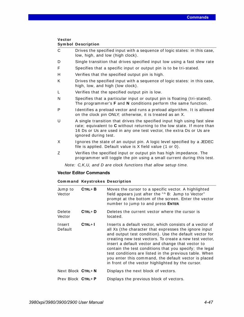
Commands
3980xpi/3980/3900/2900 User Manual 4-47
Note: C,K,U, and D are clock functions that allow setup time.
Vector Editor Commands
C Drives the specified input with a sequence of logic states: in this case, low, high, and low (high clock).
D Single transition that drives specified input low using a fast slew rate
F Specifies that a specific input or output pin is to be tri-stated.
H Verifies that the specified output pin is high.
K Drives the specified input with a sequence of logic states: in this case, high, low, and high (low clock).
L Verifies that the specified output pin is low.
N Specifies that a particular input or output pin is floating (tri-stated). The programmer's F and N conditions perform the same function.
P Identifies a preload vector and runs a preload algorithm. It is allowed on the clock pin ONLY; otherwise, it is treated as an X.
U A single transition that drives the specified input high using fast slew rate; equivalent to C without returning to the low state. If more than 16 Ds or Us are used in any one test vector, the extra Ds or Us are ignored during test.
X Ignores the state of an output pin. A logic level specified by a JEDEC file is applied. Default value is X field value (1 or 0).
Z Verifies the specified input or output pin has high impedance. The programmer will toggle the pin using a small current during this test.
Command Keystrokes Description
Jump to Vector
CTRL+B Moves the cursor to a specific vector. A highlighted field appears just after the “^B: Jump to Vector” prompt at the bottom of the screen. Enter the vector number to jump to and press ENTER.
Delete Vector
CTRL+D Deletes the current vector where the cursor is located.
Insert Default
CTRL+I Inserts a default vector, which consists of a vector of all Xs (the character that expresses the ignore input and output test condition). Use the default vector for creating new test vectors. To create a new test vector, insert a default vector and change that vector to contain the test conditions that you specify; the legal test conditions are listed in the previous table. When you enter this command, the default vector is placed in front of the vector highlighted by the cursor.
Next Block CTRL+N Displays the next block of vectors.
Prev Block CTRL+P Displays the previous block of vectors.
Vector Symbol Description
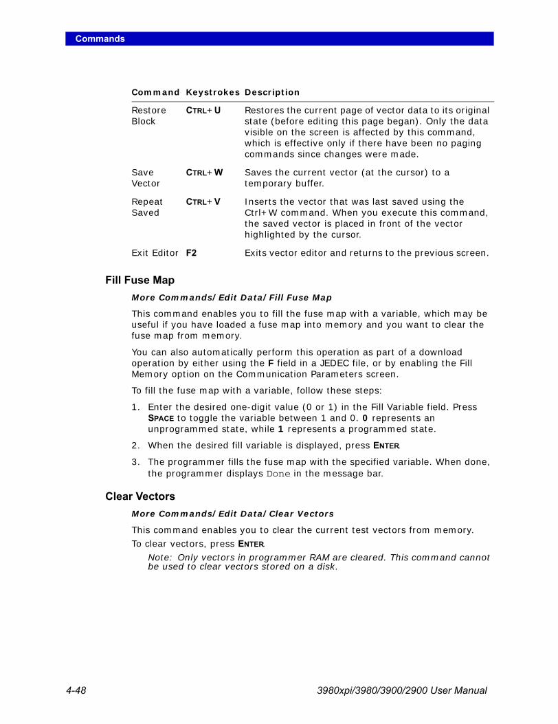
Commands
4-48 3980xpi/3980/3900/2900 User Manual
Fill Fuse Map More Commands/Edit Data/Fill Fuse Map
This command enables you to fill the fuse map with a variable, which may be useful if you have loaded a fuse map into memory and you want to clear the fuse map from memory.
You can also automatically perform this operation as part of a download operation by either using the F field in a JEDEC file, or by enabling the Fill Memory option on the Communication Parameters screen.
To fill the fuse map with a variable, follow these steps:
1. Enter the desired one-digit value (0 or 1) in the Fill Variable field. Press SPACE to toggle the variable between 1 and 0. 0 represents an unprogrammed state, while 1 represents a programmed state.
2. When the desired fill variable is displayed, press ENTER.
3. The programmer fills the fuse map with the specified variable. When done, the programmer displays Done in the message bar.
Clear Vectors More Commands/Edit Data/Clear Vectors
This command enables you to clear the current test vectors from memory. To clear vectors, press ENTER.
Note: Only vectors in programmer RAM are cleared. This command cannot be used to clear vectors stored on a disk.
Restore Block
CTRL+U Restores the current page of vector data to its original state (before editing this page began). Only the data visible on the screen is affected by this command, which is effective only if there have been no paging commands since changes were made.
Save Vector
CTRL+W Saves the current vector (at the cursor) to a temporary buffer.
Repeat Saved
CTRL+V Inserts the vector that was last saved using the Ctrl+W command. When you execute this command, the saved vector is placed in front of the vector highlighted by the cursor.
Exit Editor F2 Exits vector editor and returns to the previous screen.
Command Keystrokes Description

Commands
3980xpi/3980/3900/2900 User Manual 4-49
Edit Memory Menu The Edit Memory menu appears if you have selected a memory device. This menu contains the Edit Memory, Complement, Data Copy, Fill Memory, and Swap Memory commands.
Edit Memory More Commands/Edit Data/Edit Memory/Edit Memory Data
Use the Edit Memory command to edit the data for a memory device. To edit data stored in memory, follow these steps:1. Specify the memory editing parameters. 2. Press ENTER to enter the editor. Depending on the selected word width, the
4-, 8-, or 16-bit word width memory editor screen appears. 3. To change data, move the cursor to the memory location to be changed
and type the new characters over the old ones. Enter the data either in hex or ASCII mode (select the mode using TAB as described below). The cursor’s location is shown as a hex address at the top of the screen.
The parameters and editor commands are described below.
Source (R,D)Specifies the source of the data to be edited. Press SPACE to toggle between R (RAM) and D (Disk).
FilenameSpecifies the name of the disk file containing the data to edit. This option appears only if you select disk as the Source. The filename must follow standard DOS conventions. An example of a valid filename is 27c256.dat. The file must be an absolute binary file.
Edit Data Word Width (4,8,16,32)Selects a 4-, 8-, 16-, or 32-bit Data Word Width. Press SPACE to toggle between the 4-, 8-, and 16-bit options. If you select 8, the editor treats all addresses as byte addresses. If you select 16 or 32, the editor treats all addresses as 16- or 32-bit word addresses and the Edit Odd/Even Byte Swap feature is enabled.
Edit Address OffsetSpecifies the address you want assigned to the first byte of data in user memory. Using the address offset can save much calculation time on files written on a host system and then downloaded to the programmer. For example, if your host system data file was written using a begin address of 1000H, you could specify an offset of 1000H. Edit data would then be displayed on the programmer's screen beginning with address 1000H.
Edit Begin AddressSpecifies the first address you wish to edit. Enter the 1- to 6-digit hex address. This address must be equal to or greater than the edit address offset. The edit address offset value subtracted from the edit begin address value cannot be greater than the user RAM size.

Commands
4-50 3980xpi/3980/3900/2900 User Manual
Memory Editor Commands Only certain keyboard commands may be used in the memory editor. The allowed commands are listed in the following table.
Jump to address
CTRL+B Moves the cursor to a specific memory address. When this command is selected, the cursor moves to the Jump to Address field. Enter the address you want to jump to and press ENTER.
Delete byte CTRL+D Deletes the entire byte with 8-bit data and deletes the entire word with 16-bit data. All data after the current character position are moved one address position down. An FF is inserted at the end of RAM. If a disk file is used, the file gets smaller.
Exchange CTRL+E Allows you to search for a certain pattern and replace it with another pattern:
1. Press CTRL+E. The cursor moves to the Exchange field at the bottom of the screen.
2. Type the pattern to search for (a hex value up to 8 digits), then press ENTER. The cursor moves to the With field (bottom of screen).
3. Type the pattern you want inserted in place of the existing pattern, then press ENTER. If the pattern cannot be found, a message is displayed and the cursor remains in place.
When exchange data is entered in 4-bit mode, the upper nibble of data is blank, so only up to four characters can be entered in the field.
Next Block CTRL+N Displays the next block of memory data.
Prev Block CTRL+P Displays the previous block of memory data.
Restore Block CTRL+U Returns the current page of data to its original state (before editing began). The page is restored only if there had been no paging commands.
Search Pattern
CTRL+F Allows you to search for a particular hex pattern of up to 8 digits:
1. Press CTRL+F. The cursor moves to the Search field at the bottom of the screen.
2. Type in the pattern to search for (any hex value up to 8 digits), followed by ENTER. If the pattern cannot be found, a message is displayed and the cursor remains in its original position.
When searching for data in 4-bit mode, the upper nibble of data is blank, so only up to four characters can be entered in the search field.

Commands
3980xpi/3980/3900/2900 User Manual 4-51
Complement Data More Commands/Edit Data/Complement/Complement Memory
The Complement command converts each bit of data within the specified data block to its opposite value (one's complement). To complement data stored in memory, follow these steps:1. Specify the parameters described below.2. Press ENTER to begin the complement function. 3. The programmer displays Done when the operation is completed.
The parameters are described below.Memory AddressThe memory address at which the complement operation begins. The value entered may be any 1- to 6-digit hex address. The address cannot be greater than the User RAM size. Block SizeThe number of bytes (in hex) that is complemented. Move the cursor to the block size window and enter the block size (1 to 6 hex digits). The block size, added to the memory address, cannot exceed the user memory size.
Start/Stop Insert
CTRL+T Toggles the state between Insert and Overtype. If the Insert field is displayed in reverse video, the editor is in Insert mode. If the Insert field is displayed in normal video, the editor is in Overtype mode.
In Insert mode, data are inserted at the current cursor position and all data after that are moved up into higher memory or file addresses. If editing a RAM file, data at the end of RAM are lost. If editing a disk file, the file gets larger. The insert is not complete until the last hexadecimal character (8- or 16-bit) is entered. The cursor moves by byte for 8-bit data or by word for 16-bit data.
In Overtype mode, data entered replaces the current data. When not in insert mode, the arrow keys move the cursor by character.
For 8-bit data, the data are entered in bytes, and for 16-bit data, the data are entered in words.
Exit Editor F2 Exits the memory editor and returns the programmer to the Edit menu.
Toggle Hex/ASCII Modes
TAB Toggles the mode for data entry. When in hex mode, data are entered on the left side of the screen and the only valid entries are hex characters. When in ASCII mode, data are entered on the right side of the screen and any printable ASCII character can be entered. ASCII mode is not allowed when in 4-bit mode.

Commands
4-52 3980xpi/3980/3900/2900 User Manual
Data Copy More Commands/Edit Data/Data Copy
The Data Copy command copies a block of data from one location to another. To copy data stored in memory, follow these steps:1. Specify the parameters described below.2. Press ENTER to begin the Data Copy function. The programmer displays
Done when the operation is completed.
The parameters are described below.From Memory AddressThe first memory address of the data block you want to move data from. Enter a 1- to 6-digit hex address that does not exceed user RAM size. To Memory AddressThe first address of the data block you want to move data to. Enter a 1- to 6-digit hex address that does not exceed the user RAM size. Block SizeThe size (in hex) of the data block to move. The programmer displays a warning message if the sum of the Block Size and either the From Memory or the To Memory Address values exceeds user memory size.
Fill Memory More Commands/Edit Data/Fill Memory
The Fill Memory command fills a specified range with a 2-digit hex value. To fill a block of memory, follow these steps: 1. Specify the parameters described below.
2. Press ENTER to begin the Fill function. The programmer displays Done when the operation is completed.
The parameters are described below.Memory Begin AddressThe memory address at which the fill operation begins. Enter any 1- to 6-digit hex address. The address cannot exceed the user RAM size. Block SizeThe number of bytes (in hex) that are filled. Move the cursor to the block size window and enter the block size (from 1 to 6 hex digits). The block size, added to the memory address, cannot exceed the user memory size. Fill VariableThe 2-digit hex data variable used to fill the specified block. Enter a value between 00 and FF.
Swap Data More Commands/Edit Memory/Swap Data
The Swap Data command performs either a byte swap or a nibble swap on the data in a specified block of User RAM. To swap a block of memory, follow these steps:1. Specify the parameters described below.
2. Press ENTER to begin the Swap function. The programmer displays Done when the swap is complete.

Commands
3980xpi/3980/3900/2900 User Manual 4-53
The parameters are described below.
Swap ModeThe type of swap to perform. Choose between Byte mode and Nibble mode. In Byte mode, the high byte and the low byte will be swapped. In Nibble mode, the high order and low order nibbles will be swapped. Press SPACE to toggle between the two modes.
Memory Begin AddressThe memory address at which to begin the swap. Enter any 1- to 6-digit hex address.
Block SizeThe number of bytes (in hex) to be swapped. Enter any 1- to 6-digit hex block size. The block size, added to the memory address, cannot exceed the user memory size. Also, the block size must be an even number if using Byte mode.
File Operations More Commands/File Operations
From the File Operations menu, you can access several file manipulation and directory commands. These functions help you move and copy files, view file directories, and organize and maintain your disks. The following sections describe each of the File Operations commands in the order in which they appear on the file menu screen.
Note: A file disk has a capacity of 1.44M bytes or 112 files, whichever comes first.
View Directory More Commands/File Operations/View Directory
This command displays the file directory of the disk in the disk drive.
To view a directory, follow these steps:
1. Insert the disk you want to view into the disk drive.
2. Press ENTER to view the directory. The View Directory command can view the directory of any DOS-compatible 3.5-inch disk.
3. 28 files can be displayed at one time. If your disk has more than 28 files, they are displayed on the next page(s). Press CTRL+N to advance to the next page of files.
Load File More Commands/File Operations/Load File
This command loads a RAM Image Binary file from disk into RAM. Do not use this command to load files from a PC or from a file server. See the Download Data command for information on transferring files to the programmer from a PC or from a file server.
Note: If your files contain data formatted in other than RAM Image Binary (such as Intel Hex, Format 83e), use the Transfer Data/Input From Disk command.

Commands
4-54 3980xpi/3980/3900/2900 User Manual
To load a file into the programmer's RAM, follow these steps:1. Insert the disk containing the file you want to load into the disk drive.
2. When you select the Load File command, the dialog window displays a directory of the disk in the disk drive. If you do not see your file, press F2 to return to the File Operations menu. Insert the disk containing your file into the
3. drive and return to the beginning of this step.
4. 28 files can be displayed at one time. Press CTRL+N to advance to the next page of files.
5. Specify the parameters described below. Be sure to include a filename.
6. Press ENTER to begin loading. Once the disk file is in RAM, you may perform several operations on the file, such as edit or program device. See the appropriate sections in this chapter for more information. Note: The User Data Size field does not appear on the Load File screen. However, this parameter is still updated to reflect the size of the file loaded for use in other screens.
The parameters are described below:FilenameSpecifies the name of the disk file to load. The filename must follow standard DOS conventions. An example of a valid filename is 27c256.dat or 16l8.dat. Memory Begin AddressSpecifies the first address in memory to load data into. This option appears only if you selected a memory device. The default address is 0. If a logic device is selected, the fuse map and vectors from the disk are loaded.
Save File More Commands/File Operations/Save File
This command allows you to save the data in RAM to a disk file formatted in RAM Image Binary. Do not use this command to save a file on a PC or a file server. See the Upload Data command for information on transferring files to a PC or a file server from the programmer.
Note: A saved file is stored in RAM Image Binary format. To store a file in some other format, use the Transfer Data/Output to Disk command.
To save data in RAM to disk, follow these steps:1. Insert the disk you want to save the data to in the disk drive.2. Select Save File. A directory of the disk in the disk drive is displayed. If you
do not want to save your file to this disk, press F2 to return to the File Operations menu. Insert the disk you want to save the data to into the disk drive and return to the beginning of this step.
3. Specify the parameters described below. Be sure to include a filename.4. Press ENTER to begin the save. If you are saving information for a logic
device, the fuse map, security fuse state, and vectors are saved.

Commands
3980xpi/3980/3900/2900 User Manual 4-55
The parameters are described below:
FilenameSpecifies the name of the disk file to save RAM data to. This may be a new or existing filename you want to overwrite. If you are writing to an existing file, the current data in the file is replaced by the new data. The filename must follow standard DOS conventions (such as 27c256.dat or 16l8.dat).
Memory Begin Address (for memory devices only)Specifies the first address in RAM where data is to be saved. The default address is 0. User Data SizeSpecifies the size, in hex bytes, of the data block to save. This value is normally equal to the device size. This option appears only if you have selected a memory device.
Purge FileMore Commands/File Operations/Purge File
This command deletes a file, or group of files, from a disk. To purge a file from a disk, follow these steps:
1. Insert the disk with the file you want to delete into the disk drive.
2. When you select the Purge File command, the dialog window fills with a directory listing. The programmer displays up to 28 files at one time. If there are more than 28 files, press CTRL+N to display the next page of files. Press CTRL+P to display the first page of files. If you do not see the file you want to delete, press F2, insert another disk, and return to the beginning of this step.
3. Move the cursor to the Filename field and enter the name of the file you want to delete. Note: You can use an asterisk (*) as a wildcard. For example, to purge both 27512.dat and 27128.dat, you could type 27*.dat.
4. Move the cursor to the Are you sure? field and press Y.
CAUTION: If you do not want to delete the file, do not press Enter.
5. To delete the file, press ENTER. If you do not want to delete the file, press F2 to return to the File Operations menu.
Rename File More Commands/File Operations/Rename File
This command changes the name of a file. To rename a file, follow these steps:
1. Insert the disk with the file you want to rename into the disk drive.2. When you select the Rename File command, the dialog window fills with
the directory listing, displaying up to 28 files at a time. If there are more than 28 files, press CTRL+N to display the next page of files. Press CTRL+P to display the first page of files. If you do not see the file you want to rename, press F2, insert another disk, and return to the beginning of this step.

Commands
4-56 3980xpi/3980/3900/2900 User Manual
3. Move the cursor to the From field and enter the current name of the file you want to rename.
4. Move the cursor to the To field and enter the new name for the file you want to rename. CAUTION: If you do not want to rename the file, do not press Enter.
5. To rename the file, press ENTER. If you do not want to rename the file, press F2 to return to the File Operations menu.
Copy File More Commands/File Operations/Copy File
Use the Copy command to copy a file or a group of files. To copy a file (or group of files), follow these steps:
1. Insert the disk with the file you want to copy into the disk drive.
2. When you select the Copy File command, the dialog window fills with the directory listing. The programmer displays up to 28 files at one time. If there are more than 28 files, press CTRL+N to display the next page of files. Press CTRL+P to display the first page of files. If you do not see the file you want to copy, press F2, insert another disk, and go back to step 1.
3. Move the cursor to the From field. Enter the name of the source file.
4. Move the cursor to the To field and enter the name of the destination file.
5. Move the cursor to the Single Drive File Copy to Different Disk field.
To copy the file to a different disk, set this parameter to Y. The programmer prompts you to insert the source disk or destination disk at the appropriate times. This operation results in RAM being used as a temporary storage buffer and alters the contents of RAM.
To copy one file at a time to the same disk, set this parameter to N. Make sure the destination file has a different filename than the source file. You are prompted to swap disks when necessary. To copy a group of files, you can use an asterisk (*) as a wildcard in the name of the source and destination file.
6. To begin the copying, press ENTER.CAUTION: If you do not want to copy the file, do not press Enter. Press F2 to return to the File Operations menu.
Duplicate Disk More Commands/File Operations/Duplicate Disks
Use this command to duplicate an entire disk using the programmer. You can also duplicate a disk using DOS. These methods are described below.
Note: No matter which version you use to copy the disk, we recommend you write protect your source disk by sliding its write protect tab so you can see through the hole it exposes.

Commands
3980xpi/3980/3900/2900 User Manual 4-57
Using DOSIf you have access to a DOS-based PC with a 1.44MB 3.5-inch disk drive, we suggest that you use the DOS DISKCOPY (not the COPY) command to copy your Algorithm/System disks and Boot disk. The backup must be an exact, bit-for-bit, sector-for-sector copy of the original. For more information, see your DOS manual.
Note: If you use the DOS DISKCOPY command to duplicate a disk, make sure that the destination disk has been formatted on the programmer before the copy is made. See the More Commands/File Operations/Format Disk command for more information.
Using the ProgrammerTo use Duplicate Disk command to duplicate a disk using the programmer, follow these steps:1. Insert the disk you want to duplicate into the disk drive.
CAUTION: Do NOT use the Algorithm/System disk or the Boot disk as the destination disk because the original contents of the destination disk will be lost.
2. To duplicate the disk, move the cursor to the Are You Sure? field and press Y. (The source disk and destination disk parameters are currently fixed at A.)
CAUTION: Duplicating a disk erases the contents of the destination disk. Also, this operation uses RAM as a temporary storage buffer and alters the contents of RAM.
3. Move the cursor to the Do you want to verify disk? field and enable the disk verification procedure.To disable the verification, and speed up the process, press N. To enable the verification, press Y.
Note: Although disk duplication takes longer if the verification option is turned on, we suggest that you turn verification on while duplicating an important disk, such as the Algorithm/System disk or the Boot Files disk.
4. Finally, press ENTER to begin the disk duplication. During the duplication you are prompted when to swap disks. Note: The verification parameter returns to Y and the Are you sure? parameter returns to N after each disk duplication operation.
Format Disk More Commands/File Operations/Format Disk
Use this command to prepare a data disk for use. A disk must be formatted before it can be used.
To format a disk, follow these steps:
1. Insert the disk to be formatted into the disk drive.
2. When you are ready to format the disk, type Y ENTER at the Are You Sure? prompt. If you are not ready to format a disk, press F2 to return to the File Operations menu.

Commands
4-58 3980xpi/3980/3900/2900 User Manual
3. The programmer checks the disk in the disk drive to ensure it is not a System disk. If the programmer detects the Algorithm/System disk or the Boot disk, this message appears: WARNING: system disk in drive. Hit return to continue, ^Z to abort.
CAUTION: Do NOT format the programmer Algorithm/System disk or the Boot disk; the original contents of the disk will be lost.
4. To format the disk, press ENTER. If you do not want to format the disk, press CTRL+Z.
Job FileMore Commands/Job File
The Job File feature allows you to record a series of keystrokes that can be replayed later. You can store up to 10 job files on each System disk. Each job file can contain up to 499 keystrokes, although a typical job file contains 10 to 20 keystrokes.
Job files allow you to perform setup operations without rekeying all the parameters each time a new device is selected. For example, if you regularly program five different devices, you could create and save five different job files, each specifying particular options for a device.
You can view Job files with the View Directory command. Insert the disk with the Job file you want to use, and press F4 to display the directory for the current disk. A job file appears as JFN.JOB (N is a number between 0 and 9).
Guidelines for Constructing a Job File Because a job file does not stop until the entire file is played back, job files should not include Quick Copy commands or operations requiring a disk or base to be inserted or removed.The first command in a job file should be F1 so that it always starts from the Main Menu, preventing “runaway” job files.
Note: A job file can be used only with the version of software it was created with. If you update your software, recreate any job file created using a previous version.
Recording a Job File To record a Job file, follow these steps:
1. Press ESC CTRL+J to start recording the job file. Each keystroke entered from now on is stored in the Job file.
2. Press F1 as the first command in your Job file. (Although this is not necessary, it helps prevent “runaway” Job files.)
3. Enter all the parameters you want recorded. For example, you may want to select a device, then choose its programming parameters by using the Edit Programming Parameters command.
4. After you enter the keystrokes you want to store in the job file, press ESC CTRL+J to stop recording the job file. The Job File screen is displayed.

Commands
3980xpi/3980/3900/2900 User Manual 4-59
5. Select a file number for the newly created job file. For example, to make this job file number five on the Job Files screen, press 5 ENTER. If you select a file number already in use, the programmer prompts you to press ENTER to overwrite the existing file. To preserve the existing file, press CTRL+Z.
6. Move the cursor down to the Enter Description field and type a name for the job file that was just recorded. The description can be up to 31 characters long and should be followed by ENTER.To save the job file, press ENTER. While the file is being saved, the action symbol rotates. When the save action is done, you are returned to the last screen displayed during job file recording.If you do not want to save the job file, press F2 or F1.
Playing Back a Job File More Commands/Job File
Use the Job File command to play back a pre-recorded job file. To play back a job file, follow these steps:
1. Go to the Job Files screen. 2. You see a listing of the job files stored on the Algorithm/System disk in the
disk drive. To select a job file from this disk, type the number of the job file you want to play back and press ENTER. For example, to play back the fifth file on the list, press 5 ENTER.To view a list of job files stored on another disk, insert the disk and press F4, which reconstructs the job file directory.
3. The programmer now plays back the keystrokes that were recorded. Each screen displayed while you were recording keystrokes is shown (briefly).
4. After the job file is played back, the programmer displays the following message: Job file playback ended.
The last screen recorded while you were creating the job file is now displayed. If an error occurred during playback, an error message is displayed and the job file must be re-recorded.
Remote ControlMore Commands/Remote Control/CRC Mode
This command puts the programmer in Computer Remote Control mode. To exit remote control, type CTRL+Z on the terminal's keyboard, or send a Z ENTER command from the host computer. Chapter 2, Setting Up, describes how to set up your system. Appendix B, Computer Remote Control, provides information on how to use CRC and describes the CRC command set.

Commands
4-60 3980xpi/3980/3900/2900 User Manual
Self-test More Commands/Self-test
The Self-test command allows you to test subsystems in the programmer, verifying proper operation or isolating possible problem areas. An automatic self-test is also performed each time the programmer is powered up. If errors occur during the powerup test, the Self-test screen is displayed, showing the areas that failed. Some self-tests (such as User RAM test) can be disabled so they are not checked during powerup. Disabling and enabling self-tests is done in the More Commands...Interface menu.
Note: For details (help) on the function of each self-test, move the cursor to the test you want information about and press F3.For information on how to verify the performance of your programmer, refer to Appendix A.
Halting a Self-test You can stop a self-test at anytime during its operation by pressing CTRL+Z.
Running the Self-test To perform a Self-test, follow these steps:1. Make sure the device socket is empty.2. Select the test mode. You can select either one-pass or continuous testing.
To toggle modes, move the cursor to the Test Mode field and press SPACE. One Pass testing runs the specified test once. Continuous testing runs the specified test until there is a failure or until you halt the procedure by pressing CTRL+Z. Note: There may be a delay before the programmer responds to the Ctrl+Z if the programmer is running the system RAM test.
3. To test all hardware, move the cursor to the Perform All Tests prompt and press ENTER.
To test a particular item, move the cursor to the desired test and press ENTER.
Interpreting Self-test Results Four conditions are used as status indicators on the self-test screen:
? UNTESTEDP PASSF FAIL- NOT INSTALLED
When testing begins, a ? appears next to the untested areas. As each test completes, either P (pass) or F (fail) appears next to the test name, showing the results of the test performed. If a hardware item is not installed, a — appears. During testing, the message area of the self-test screen indicates that testing is in progress. During the System RAM test, the Remote and the Terminal indicators blinks to indicate that testing is in progress.

Commands
3980xpi/3980/3900/2900 User Manual 4-61
If ? symbols still appear next to some test names when the testing has completed, it may be because some other test(s) need to pass before the indicated one may be tested. For example, the waveform circuit test must pass before the pin control unit test executes.
Note: All the installed programmer hardware must pass self-test before any other operations can take place.
Transfer DataMore Commands/Transfer Data
Use the commands on the Transfer Data menu to move data files back and forth between the programmer and a host computer.
The Transfer Data menu contains the following seven commands: Download Data, Upload Data, Compare Data, Format Select, Input From Disk, Output to Disk, and Serial Output. Each of these commands is described in this section.
Download Data More Commands/Transfer Data/Download Data
Use the Download Data command to specify downloading parameters and to execute the download operation. Downloading moves a data file from a host computer to the programmer's RAM or disk.
Before you download data, specify the variables for the following parameters, then enter a command in the Download Host Command field. The information in the command line is a command that your host computer (the computer containing the file to download) recognizes as an instruction to begin the download operation. Finally, press ENTER to execute the download. When the download is complete, the programmer displays Data transfer complete.
Source (R,T)Specifies what programmer port is connected to your host computer. Press SPACE to toggle between R (Remote port) and T (Terminal port).
Destination (R,D)Specifies the destination of the data that is being downloaded from the host computer. Press SPACE to toggle between R (RAM) and D (disk).
FilenameSpecifies the name of the disk file in which to save the downloaded file. This option appears only if you specify Disk as the Destination. The filename must follow standard DOS conventions (such as 27256.dat). I/O Translation FormatSelects the translation format of the data in the file. A list of formats the programmer supports is available on the Format Select screen in the Transfer Data menu, and also in the front of Chapter 5. If you know the number for your format, enter it from this screen. If you do not know the number of the format you are using, use the Format Select command to select the format. If you are using the Altera POF format, you must select the desired POF device before you perform a data transfer operation.

Commands
4-62 3980xpi/3980/3900/2900 User Manual
I/O Addr OffsetEnter the beginning hex address of the host computer's data file or the first address you want to capture within a file. This field appears only when a non-JEDEC format has been selected. The programmer subtracts this address from addresses received to determine where, either in the user RAM or in the disk file, the data will be loaded. Entering FFFFFFFF sets the first address received as the I/O offset for the rest of the download. Memory Begin AddressSpecifies the first address, in hex, where the first byte of data is stored from the source port. This field appears only when a non-JEDEC format is selected. If the destination is RAM, it is a beginning RAM address; if the destination is disk, it is a beginning disk file address. The default is 0. User Data SizeSpecifies the hexadecimal size, in bytes, of the data block to be downloaded. This field appears only when a non-JEDEC format has been selected. The default is 0, which directs the programmer to receive all the data in the file. After the download is complete, a value equal to the number of bytes received is set here. If a value less than the size of the data received is entered, only the number of bytes equal to that value are actually stored.
Download Host CommandEnter the appropriate host command line here to download the data. This line may be up to 58 characters long. The programmer generates a return character to terminate the line when transmitted to the host. To clear a previously entered command, enter a blank command by pressing SPACE.
If you are using HiTerm, use the tr filename command, where filename is the name of the file to download. For more information, see the HiTerm User Manual. For an example of using HiTerm to download data from a PC, see Session 8 in Chapter 3.
Upload Data More Commands / Transfer Data / Upload Data
Use the Upload Data command to specify uploading parameters and to execute the upload operation. Uploading moves a data file from the programmer's RAM or disk to the host computer.
To upload a data file, follow these steps:
1. Specify the variables for the parameters listed below.
2. Enter a command in the Upload Host Command field. The information in the command line is a command that your host computer (the computer receiving the data file) recognizes as an instruction to begin the upload operation.
3. Press ENTER to start the upload. During the upload, the action symbol rotates. When done with the upload, the programmer displays the following message: Data Transfer complete. Data sum = xxxxxxxx.

Commands
3980xpi/3980/3900/2900 User Manual 4-63
The parameters are described below.
Source (R,D)Specifies where the data to be uploaded is located. Press SPACE to toggle between R (RAM) and D (disk).
FilenameSpecifies the name of the disk file to upload to the host. This option appears only if you specify Disk as the Source. The filename must follow standard DOS conventions (such as 27256.dat).
Destination (R,T)Specifies which port the data file is sent through. Press SPACE to toggle between R (Remote Port) and T (Terminal Port).
I/O Translation FormatSpecifies the translation format in which the file is to be generated. The format specified here must be the same as that expected by the host computer. A list of formats supported by the programmer appears on the Format Select screen in the Transfer Data menu in Chapter 5. If you know the number for your format, you can enter it from this screen. If you do not know the format number, go to the Format Select screen, find the format you want and enter the number from that screen. Entering the format number from the Format Select screen changes the Translation Format parameter on this screen.
I/O Addr OffsetEnter the beginning address of the upload file. This field appears only when a non-JEDEC format has been selected. This value is added to the address of the data in memory (relative to the Memory Begin Address of 0) and output as the I/O address. A value of FFFFFFFF sets the I/O Offset to 0.
Memory Begin AddressSpecifies the first address, in hex, from where the first byte of data is retrieved. This field appears only when a non-JEDEC format has been selected. If the source is RAM, it is a beginning RAM address. If the source is Disk, it is a beginning disk file address. The default address is 0.
User Data SizeSpecifies the hexadecimal size, in bytes, of the data block to be uploaded. This field appears only when a non-JEDEC format has been selected. Enter the value of the number of bytes to upload. Entering 0 directs the programmer to upload the entire contents of the programmer's RAM. Or, if Disk is specified as the Source, entering 0 directs the programmer to upload the entire disk file.
Upload Host CommandEnter the appropriate host command line (up to 58 characters) to direct the host to accept the uploaded data. The programmer generates a return character to terminate the line when transmitted to the host. To clear a previously entered command, press SPACE ENTER.

Commands
4-64 3980xpi/3980/3900/2900 User Manual
Compare Data More Commands / Transfer Data / Compare Data
The Compare Data command compares data in user memory with the data file downloaded from the host computer. You can use this command to verify that you transferred a complete and accurate copy of a data file. The current I/O format is used to translate the incoming data from the serial port. (JEDEC format cannot be used with this command.) This operation is similar to the download operation, except data is compared with, rather than written to, memory.
1. Before you compare data, specify variables for parameters listed below.
2. Enter a command in the Download Host Command field. The information in the command line is a command that your host computer recognizes as an instruction to begin the download operation.
3. Press ENTER to run the command. One of these messages is displayed.
The parameters are described below.
Source (R,T)Specifies which of the programmer's ports is connected to the computer with the data file that is to be compared with the memory data. Press SPACE to toggle between R (Remote port) and T (Terminal port).
Data Location (R,D)Specifies where the data to be compared is located. Press SPACE to toggle between R (RAM) or D (Disk).
FilenameSpecifies the name of the disk file you want compared. This option appears only if you specify Disk as the Source. The filename must follow standard DOS conventions (such as 27256.dat).
I/O Translation FormatSpecifies the data translation format of the data in the file. If you know the number for your format, you can enter it from this screen. If you do not know the format number, find the format you want to use on the Format Select screen and enter the format number from. Entering the format number from the Format Select screen changes the Translation Format parameter on this screen.
Message Condition
Data transfer complete. The two data files are identical.
Data verify error. Data sum = xxxxxxxx.
The two data files are not identical.
Compare fail at AAAAAA:XX not YY (AAAAAA=address, XX=memory data, YY=host's data)
Data in memory does not match data sent from the host and the terminal is not on the same port as the port receiving the data from the host.
Data verify error. Data sum = ssssssss.
The terminal is on the same port.

Commands
3980xpi/3980/3900/2900 User Manual 4-65
I/O Addr OffsetSpecifies the beginning address of the downloaded data file to be compared. This field appears only when a non-JEDEC format has been selected. Entering FFFFFFFF causes the programmer to default to the first incoming address as the lowest address to be compared. Memory Begin AddressSpecifies the first hexadecimal address of data to compare with data from the Source port. If the data location is RAM, it is a beginning RAM address. If the data location is Disk, it is a beginning disk file address. This field appears only when a non-JEDEC format has been selected. The default address is 0. User Data SizeSpecifies the hexadecimal size, in bytes, of the data block to be downloaded and compared from the Source to the data location. This field appears only when a non-JEDEC format has been selected. Normally, you should enter a zero here so all the data is compared. After the compare operation is complete, a value equal to the number of bytes compared is set here. If a value less than the size of the data received is entered, only the number of bytes equal to that value are actually compared. Download Host CommandEnter the appropriate host command line here to download the data. This line may be up to 58 characters long. The programmer generates a return character to terminate the line when transmitted to the host. To clear a previously entered command, press SPACE then ENTER.
Format Select More Commands / Transfer Data / Format Select
The Format Select command selects the translation format to use. Translation formats (a form of transmission protocol) are used when data is uploaded or downloaded between the programmer and a host computer. Chapter 5 lists and describes the formats supported by the programmer. If your host computer does not generate code into one of the listed formats, edit it to match one of the supported formats. The Format Select screen lists the programmer supported formats to choose from. Enter the number of the format that you want to use in the format entry field at the bottom of the screen, then press ENTER. When you select a translation format from this screen, the same format is entered in all the other Transfer Data screens (such as, Download Data and Compare Data).
Input From Disk More Commands / Transfer Data / Input From Disk
Use this command to load a data file from disk if the data is stored in a translation format. Depending on the settings of the Destination parameter, the data in the disk file is loaded into either RAM or another disk file.
To input a data file from disk, follow these steps:
1. Insert the disk containing the file to input into the drive.2. Specify the settings for the parameters listed below.
3. Press ENTER to start this command. The programmer displays Data transfer complete when the file has been loaded.

Commands
4-66 3980xpi/3980/3900/2900 User Manual
The following parameters are available: Input FilenameSpecifies the name of the disk file from which formatted data are taken. The filename must follow standard DOS conventions (such as 27256.hex).Destination (R,D)Specifies the destination for the data. Press SPACE to toggle between R (RAM) and D (another disk file). FilenameSpecifies the filename for the disk file into which data are sent. This option appears only if you specify Disk as the Destination. The filename must follow standard DOS conventions. I/O Translation FormatSpecifies the format of the data to be input. See Chapter 5 for a complete list of supported formats. I/O Address OffsetEnter the beginning hex address, or the first address you want to capture within a file, of the disk file's data. This field appears only if a non-JEDEC format has been selected. The programmer subtracts this address from addresses received to determine where the data is loaded into memory. Entering FFFFFFFF sets the I/O Offset equal to the first address received. Memory Begin AddressSpecifies the first address, in hex, to which the first byte of data is stored in memory. If the destination is RAM, it is a beginning RAM address. If the destination is Disk, it is a beginning disk file address. The default address is 0. This field appears only if a non-JEDEC format has been selected. User Data SizeThe User Data Size specifies how many bytes (in hex) are read during the Input from Disk operation. The default User Data Size is 0, which causes all the data to be input. After the operation is complete, the programmer updates the User Data Size parameter to reflect the number of bytes stored to the destination. If a value less than the size of data file input is entered, the number of bytes equal to that value are actually stored. This field appears only if a non-JEDEC format has been selected.
Output To Disk More Commands/Transfer Data/Output to Disk
The Output To Disk command saves data from a disk file or from RAM to another disk file. The data in the newly created disk file can be stored in any of the supported translation formats. So, you could save an existing data file in another translation format. This command is similar to Upload Data, except that the formatted data is sent to a disk file rather than a port.
Follow these steps to output data in a translation format and store it on a disk. 1. Use the View Directory command on the File Menu to make sure there is
enough space on the disk in the drive to hold the file you are writing.2. Specify the settings for the parameters listed below.
3. Press ENTER to start this command. The programmer displays Data transfer complete after the file is output to the disk.

Commands
3980xpi/3980/3900/2900 User Manual 4-67
The following parameters are available: Source (R,D)Select the Source for the disk file data. Press SPACE to toggle between R (RAM) and D (disk). FilenameSpecifies the name of the disk file from which the data are taken. This option appears only if Disk is selected as the Source. The filename parameter must follow standard DOS conventions (such as 27256.dat). Output FilenameSpecifies the name of the disk file you want the formatted data sent to. The filename must follow standard DOS conventions (such as 27256.hex). I/O Translation FormatSpecifies the translation format for the data. A complete listing of the formats is given in the Translation Formats chapter of this manual. I/O Address OffsetEnter the desired beginning address of the disk file. This field appears only if a non-JEDEC format has been selected. The programmer adds this value to the address of the data in memory (relative to the Memory Begin Address of 0) and outputs the sum as the I/O address. Entering FFFFFFFF sets the I/O Address Offset to 0. Memory Begin AddressSpecifies the first address, in hex, from which the first byte of data is retrieved to write to the disk output file. If the source is RAM, it is a beginning RAM address. If the source is Disk, it is a beginning disk file address. The default address is 0. This field appears only if a non-JEDEC format has been selected.
User Data SizeSpecifies the hexadecimal size, in bytes, of the data block to be output, with translation, to the output file from the source. Enter the number of bytes to output. Entering zero sets User Data Size to the total number of hex bytes in the programmer User RAM, or the size of the source disk file if disk is used as source. This field appears only if a non-JEDEC format has been selected.
Serial Output More Commands/Transfer Data/Serial Output
Use the Serial Output command to send data from the programmer to a serial device, such as a printer.
Use this command to obtain a quick copy of programming or other device-related data. Serial Output does not do any data translating. If a logic device is selected, the fuse data are output by fuse number and the vectors are output by vector number. If a memory device is selected, the data are output by address in hex format.
Output Memory Data to Serial Port More Commands/Transfer Data/Serial Output/Output Memory Data
When a memory device has been selected, the Serial Output command is output as a specified memory block to one of the programmer's serial ports.

Commands
4-68 3980xpi/3980/3900/2900 User Manual
The parameters for this command are listed below.Source (R,D)Specifies the source for the data. Press SPACE to toggle between R (RAM) and D (Disk). FilenameSpecifies the disk file to use as the Source. This option appears only if you specify Disk as the Source. The filename must follow standard DOS conventions. An example of a valid filename is 27128a.dat.Destination (R,T)Specifies the destination for the data. Press SPACE to toggle between R (Remote port) and T (Terminal port). Number Of Lines Between Form FeedsSpecifies the number of printed text lines per page. Default is 0 (no form feed). Memory Begin AddressSpecifies the first address, in hex, of the first byte of data to be retrieved and sent out the serial port. If the source is RAM, it is a beginning RAM address. If the source is Disk, it is a beginning disk file address. The default address is 0. User Data SizeSpecifies the hexadecimal size, in bytes, of the data block to be output. Enter the number of bytes to output. Entering zero sets the User Data Size to the total number of bytes in the programmer User RAM, or the size of the source disk file if the disk is used as the source.
Output Logic Data to Serial Port More Commands / Transfer Data / Serial Output / Output Logic Data
If you selected a logic device, the Output Logic Data to Serial Port screen is displayed. Enter the parameters you want to use, then press ENTER to begin the transfer. The parameters for this screen are described below
Source (R,D)Specifies the source for the data. Press SPACE to toggle between R (RAM) and D (Disk). FilenameSpecifies the disk file to use as the data source. This field appears only if you specify Disk as the Source. The filename must follow standard DOS conventions. An example of a valid filename is 16l8.dat. Destination (R,T)Specifies the destination for the data. Press SPACE to toggle between R (Remote port) and T (Terminal port). Number Of Lines Between Form FeedsSpecifies the number of printed text lines you wish to have per page. The default is 0 (no form feed). Starting Vector NumberSpecifies the first vector to be output. The default is 1, which causes the vector listing to start at the first vector. Number Of VectorsSpecifies the total number of vectors you wish to output. The default is 0, which causes no vectors to be output.

Commands
3980xpi/3980/3900/2900 User Manual 4-69
Yield TallyMore Commands / Yield Tally / Yield Tally Output
The Yield Tally command allows you to maintain programming information on devices that have been programmed, which is useful in a manufacturing environment where device yield statistics must be kept. Yield statistics are maintained on the last 16 device types programmed. When you run Yield Tally on the 17th device, the statistics for the oldest device are dropped. The yield tally record uses the manufacturer name and part number as the device name. The yield data is stored on the Algorithm/System disk or the 3980 hard drive in the ytally.ytl file. If the file does not exist, enabling the Yield Tally option creates a blank copy of this file on the disk.
Note: To upload the yield statistics in CRC mode, use command 43]. The CRC command 46] clears the yield tally statistics. See Appendix B.
Space is allocated on the Algorithm/System disk for the Yield Tally data files. When the Yield Tally function is run and the Algorithm/System disk is not in the disk drive, the error message FILE ERROR: Cannot access yield data is displayed on the terminal. In CRC mode, the programmer responds with error code 9A if the Algorithm/System disk cannot be found.
Yield TotalThe Yield Total includes only those devices with the following error conditions: illegal bit, misverify, device not programmable, and structured test failure. (Examples of these conditions are Continuity Check and Electronic ID Error.)
The Yield Tally screen provides statistics for the following categories:
Device NameManufacturer's name and part number. Statistics for the last sixteen device types are kept.Total CountThe number of individual devices of the same type that the programmer attempted The number of devices successfully programmed.Illegal BitThe number of devices that failed because they did not pass non-blank test or Illegal Bit Check.Verify FailThe number of devices that failed because they did not verify.Struct FailThe number of logic devices of the same type that failed the logic structured vector test.Device Not ProgrammableThe number of devices that could not be programmed because they contained bits that required more programming pulses than were specified.
If you stop the non-blank test without programming the device, the illegal bit count increases by one. If you continue the test, the illegal bit count stays the same while the yield tally records the result of the programming operation.To erase the entire set of statistics, press CTRL+E. To go to the previous menu, press F2. To go to the Main Menu, press F1. For the total number of errors, which is not recorded, add the values in the error columns.

Commands
4-70 3980xpi/3980/3900/2900 User Manual
Transparent Mode Transparent mode can be entered from all programmer screens except:
Editor screensUnder/over-blow screenYield Tally screenHelp screensCRC mode
In Transparent mode you can communicate with a host computer connected to one of the programmer ports. This mode causes the terminal connected to the other programmer port to act as if it were connected directly to the host computer. Use this mode to establish communication with the host (such as logging in and running commands).
To enter and exit this mode, type ESC CTRL+T from the terminal. Transparent mode does not support binary data transfers (this can be done via the Upload and Download commands using one of the binary data formats). See page 2-7 for more information.
In Transparent mode, all key strokes entered on the terminal are passed directly to the host with one exception. The ESC character omitted since it is part of the Exit Transparent Mode command.
To send an ESC character to the host, enter two consecutive ESC characters (the second one is passed to the host), or if ESC is followed by some character other than a CTRL+T, the escape and the character are sent to the host.

3980xpi/3980/3900/2900 User Manual 5-1
5 Translation Formats
IntroductionWhen a data file (which contains information to be programmed into a device) is created, it is stored in a specific data translation format. When the data file is transferred to a programmer, it must be set to handle the appropriate translation format. During download, the programmer translates the formatted data and stores it in user memory as a binary image file. The following translation formats are described in this chapter.
Format Code Page
ASCII-BNPF 01 (05*) 5-3ASCII-BHLF 02 (06*) 5-3ASCII-B10F 03 (07*) 5-3Texas Instruments SDSMAC (320 04 5-45-level BNPF 08 (09*) 5-5Formatted Binary 10 5-6DEC Binary 11 5-7Spectrum 12 (13*) 5-8POF 14 5-9Absolute Binary 16 5-11LOF 17 5-12ASCII - Octal Space 30 (35*) 5-14ASCII - Octal Percent 31 (36*) 5-14ASCII - Octal 5-14Apostrophe 32 5-14ASCII - Octal SMS 37 5-14ASCII - Hex Space 50 (55*) 5-14ASCII - Hex Percent 51 (56*) 5-14ASCII - Hex Apostrophe 52 5-14ASCII - Hex SMS 57 5-14ASCII - Hex Comma 53 (58*) 5-14RCA Cosmac 70 5-16Fairchild Fairbug 80 5-17MOS Technology 81 5-18Motorola EXORcisor 82 5-19Intel Intellec 8/MDS 83 5-20Signetics Absolut Object 85 5-20Tektronix Hexadecimal 86 5-21Motorola EXORmax 87 5-22Intel MCS-86 Hex Object 88 5-23Hewlett-Packard 64000 Absolute 89 5-25Texas Instruments SDSMAC 90 5-26JEDEC Format (Full) 91 5-27 and 5-30JEDEC Format (Kernel) 92 5-27 and 5-37 Tektronix Hexadecimal Extended 94 5-37Motorola 32 bit (S3 Record) 95 5-39Hewlett-Packard UNIX Format 96 5-40Intel OMF 386 97 5-41Intel OMF 286 98 5-42Intel Hex-32 99 5-44
* This alternate code is used to transfer data without the STX start code and the ETX end code.** This alternate code is used to transfer data using the SOH start code instead of the usual STX.

Translation Formats
5-2 3980xpi/3980/3900/2900 User Manual
Instrument Control CodesThe instrument control code, a 1-digit number that signals or controls data transfers, can be used to provide peripherals with flow control beyond that provided by software handshaking. The instrument control code is sent immediately preceding the 2-digit format code in computer remote control. The three instrument control codes and their functions are described below.
Note:X-ON character is a CTRL-Q, or 11 hex.X-OFF character is a CTRL-S, or 13 hex.PUNCH-ON character is a CTRL-R, or 12 hex.PUNCH-OFF character is a CTRL-T, or 14 hex.
General NotesCompatibilityWhen translating data, you may use any remote source that produces formats compatible with the descriptions listed in this section.
Formats with Limited Address FieldsSome formats are not defined for use with address fields greater than 64K. If you transfer a block greater than 64K, the address fields that would be greater than 64K may wrap around and overwrite data transferred in previous data records. Formats 70 through 86, and 90 may exhibit this characteristic.
Hardware Handshaking If compatible with the host interface, hardware handshaking may be used by connecting the appropriate lines at the serial port interface. Hardware handshake (CTS/DTR) is enabled as the default. If those signals aren't connected, however, the programming electronics communicates using software handshake (XON/XOFF). The programmer always uses software handshake regardless of whether hardware handshake is enabled.
Leader/TrailerDuring output of all formats except 89 (HP 64000), a 50-character leader precedes the formatted data and a 50-character trailer follows. This leader/trailer consists of null characters. If null count is set to FF hex, the leader/trailer is skipped. To set the null count, go to More Commands/Configure/Edit/Communication Parameters, or use the U command when using CRC.Note: Formats 10, 11, and 89 do not function properly unless you select NO parity and 8-bit data.
Code Input Function Output Function
0HandshakeOff
Send X-OFF to stop incoming transmission. Send X-ON to resume transmission.
Data transmission is halted on receipt of an X-OFF character. Transmission resumes on receipt of an X-ON character.
1HandshakeOn
Transmit an X-ON character when ready to receive data; transmit X-OFF if the receiver buffer is full; transmit an X-ON if the receiver buffer is empty; transmit an X-OFF after all the data is received.
Transmit a PUNCH-ON character prior to data transmission. Data transmission is halted on receipt of an X-OFF character and resumes on receipt of an X-ON character. A PUNCH-OFF character is sent when the transmission is completed.
2X-ON/X-OFF
Send X-OFF to stop the incoming transmission. Send X-ON to resume transmission.
Transmit data only after receiving an X-ON character. Data transmission will be halted upon receipt of an X-OFF character; transmission will resume upon receipt of an X-ON character.

Translation Formats
3980xpi/3980/3900/2900 User Manual 5-3
ASCII Binary Format, Codes 01, 02, and 03 (or 05, 06, and 07)In these formats, bytes are recorded in ASCII codes with binary digits represented by Ns and Ps, Ls and Hs, or 1s and 0s respectively. See Figure 5-1. The ASCII Binary formats do not have addresses.
Figure 5-1 shows sample data bytes coded in each of the three ASCII Binary formats. Incoming bytes are stored sequentially in RAM starting at the first RAM address. Bytes are sandwiched between B and F characters and are separated by spaces.
Data can also be expressed in 4-bit words. The programmer generates the 4-bit format on upload if the data word width is 4 bits. You can insert any other character, such as carriage returns or line feeds, between an F and the next B.The start code is a nonprintable STX (a CTRL-B, same as a hex 02). The end code is a nonprintable ETX (a CTRL-C, same as a hex 03).
Note: Data without a start or end code may be input to or output from the programmer by use of alternate data translation format codes. These are ASCII-BNPF, 05; ASCII-BHLF, 06; ASCII-B10F, 07.
Figure 5-1. ASCII Binary Format (example)
BPPPPPPPPF BPPPPPPPPF BPPPPPPPPF BPPPPPPPPFBPPPPPPPPF BPPPPPPPPF BPPPPPPPPF BPPPPPPPPFBPPPPPPPPF BPPPPPPPPF BPPPPPPPPF BPPPPPPPPFBPPPPPPPPF BPPPPPPPPF BPPPPPPPPF BPPPPPPPPFBPPPPPPPPF BPPPPPPPPF BPPPPPPPPF BPPPPPPPPFBPPPPPPPPF BPPPPPPPPF BPPPPPPPPF BPPPPPPPPFBPPPPPPPPF BPPPPPPPPF BPPPPPPPPF BPPPPPPPPFBPPPPPPPPF BPPPPPPPPF BPPPPPPPPF BPPPPPPPPF
2FORMAT 01 (OR 05)
BHHHHHHHHF BHHHHHHHHF BHHHHHHHHF BHHHHHHHHFBHHHHHHHHF BHHHHHHHHF BHHHHHHHHF BHHHHHHHHFBHHHHHHHHF BHHHHHHHHF BHHHHHHHHF BHHHHHHHHFBHHHHHHHHF BHHHHHHHHF BHHHHHHHHF BHHHHHHHHFBHHHHHHHHF BHHHHHHHHF BHHHHHHHHF BHHHHHHHHFBHHHHHHHHF BHHHHHHHHF BHHHHHHHHF BHHHHHHHHFBHHHHHHHHF BHHHHHHHHF BHHHHHHHHF BHHHHHHHHFBHHHHHHHHF BHHHHHHHHF BHHHHHHHHF BHHHHHHHHF
2FORMAT 02 (OR 06)
B11111111F B11111111F B11111111F B11111111FB11111111F B11111111F B11111111F B11111111FB11111111F B11111111F B11111111F B11111111FB11111111F B11111111F B11111111F B11111111FB11111111F B11111111F B11111111F B11111111FB11111111F B11111111F B11111111F B11111111FB11111111F B11111111F B11111111F B11111111FB11111111F B11111111F B11111111F B11111111F
2
1
3
1
3
1
3
FORMAT 03 (OR 07)
LEGEND
Start Code - nonprintable STX - CTRL B is the optional Start Code
Characters such as spaces, carriage returns and line feeds may appear between bytes
End Code - nonprintable ETX - CTRL C
1
2
3 0074-2
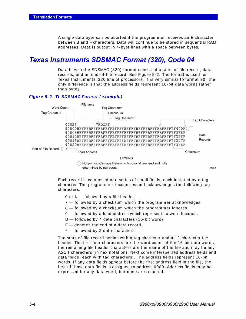
Translation Formats
5-4 3980xpi/3980/3900/2900 User Manual
A single data byte can be aborted if the programmer receives an E character between B and F characters. Data will continue to be stored in sequential RAM addresses. Data is output in 4-byte lines with a space between bytes.
Texas Instruments SDSMAC Format (320), Code 04Data files in the SDSMAC (320) format consist of a start-of-file record, data records, and an end-of-file record. See Figure 5-2. The format is used for Texas Instruments' 320 line of processors. It is very similar to format 90; the only difference is that the address fields represent 16-bit data words rather than bytes.
Each record is composed of a series of small fields, each initiated by a tag character. The programmer recognizes and acknowledges the following tag characters:
0 or K — followed by a file header.7 — followed by a checksum which the programmer acknowledges.8 — followed by a checksum which the programmer ignores.9 — followed by a load address which represents a word location.B — followed by 4 data characters (16-bit word).F — denotes the end of a data record.* — followed by 2 data characters.
The start-of-file record begins with a tag character and a 12-character file header. The first four characters are the word count of the 16-bit data words; the remaining file header characters are the name of the file and may be any ASCII characters (in hex notation). Next come interspersed address fields and data fields (each with tag characters). The address fields represent 16-bit words. If any data fields appear before the first address field in the file, the first of those data fields is assigned to address 0000. Address fields may be expressed for any data word, but none are required.
Figure 5-2. TI SDSMAC Format (example)
00028 7FDCFF90000BFFFFBFFFFBFFFFBFFFFBFFFFBFFFFBFFFFBFFFF7F400F90008BFFFFBFFFFBFFFFBFFFFBFFFFBFFFFBFFFFBFFFF7F3F8F90010BFFFFBFFFFBFFFFBFFFFBFFFFBFFFFBFFFFBFFFF7F3FFF90018BFFFFBFFFFBFFFFBFFFFBFFFFBFFFFBFFFFBFFFF7F3F7F90020BFFFFBFFFFBFFFFBFFFFBFFFFBFFFFBFFFFBFFFF7F3FEF:
Tag Character
Word Count Tag Character
Checksum
Tag Character
Filename
End-of-File RecordLoad Address
Tag Characters
DataRecords
Checksum
0429-2
LEGEND
Nonprinting Carriage Return, with optional line feed and nullsdetermined by null count.

Translation Formats
3980xpi/3980/3900/2900 User Manual 5-5
The record ends with a checksum field initiated by the tag character 7 or 8, a 4-character checksum, and the tag character F. The checksum is the two's complement of the sum of the 8-bit ASCII values of the characters, beginning with the first tag character and ending with the checksum tag character (7 or 8).
Data records follow the same format as the start-of-file record but do not contain a file header. The end-of-file record consists of a colon (:) only. The output translator sends a CTRL-S after the colon.
During download or input from disk operations, the destination address for the data is calculated in the following manner:
Memory address = (load address x 2) — I/O address offset + begin address
During upload or output to disk operations, the load address sent with each data record is calculated in the following manner:
Load address = I/O address offset / 2
The Memory begin address, I/O address offset, and User data size parameters represent bytes and must be even values for this format. The upload record size must also be even for this format (default is 16).
Note: If the data will be programmed into a 16-bit device to be used in a TMS320 processor-based system, the odd/even byte swap switch must be enabled.
5-Level BNPF Format, Codes 08 or 09Except for the start and end codes, the same character set and specifications are used for the ASCII-BNPF and 5-level BNPF formats.
Data for input to the programmer is punched on 5-hole Telex paper tapes to be read by any paper tape reader that has an adjustable tape guide. The reader reads the tape as it would an 8-level tape, recording the 5 holes that are on the tape as 5 bits of data. The 3 most significant bits are recorded as if they were holes on an 8-level tape. Tape generated from a telex machine using this format can be input directly to a serial paper tape reader interfaced to the programmer. The programmer's software converts the resulting 8-bit codes into valid data for entry in RAM.
The start code for the format is a left parenthesis, (Figs K on a telex machine), and the end code is a right parenthesis, (Figs L on a telex machine). The 5-level BNPF format does not have addresses.
Note: Data without a start or end code may be input to or output from the programmer by use of the alternate data translation format code, 09. This format accepts an abort character (10 hex) to abort the transmission.

Translation Formats
5-6 3980xpi/3980/3900/2900 User Manual
Formatted Binary Format, Code 10Data transfer in the Formatted Binary format consists of a stream of 8-bit data bytes preceded by a byte count and followed by a sumcheck, as shown in Figure 5-3. The Formatted Binary format does not have addresses.
The programmer stores incoming binary data upon receipt of the start character. Data are stored in RAM starting at the first RAM address specified by the Memory Begin Address parameter and ending at the last incoming data byte.
Figure 5-3. Formatted Binary Format (example)
2 BYTE HEX SUMCHECK (02FB)
2 NULLS
BINARY DATA
BIT8 BIT
1
RUBOUT (START CODE)
4 NIBBLE HEX BYTE COUNT
1 NULL
ARROWHEAD
08492A1C08
0200
0020 HEX(32 DECIMAL)
HIGHORDER
LOWORDER
0075-2

Translation Formats
3980xpi/3980/3900/2900 User Manual 5-7
A paper tape generated by a programmer contains a 5-byte, arrow-shaped header followed by a null and a 4-nibble byte count. The start code, an 8-bit rubout, follows the byte count. The end of data is signaled by two nulls and a 2-byte sumcheck of the data field. Refer to Figure 5-4.
If the data output has a byte count GREATER than or equal to 64K, an alternate arrow-shaped header is used. This alternate header (shown below) is followed by an 8-nibble byte count, sandwiched between a null and a rubout. The byte count shown here is 40000H (256K decimal). If the byte count is LESS than 64K, the regular arrowhead is used instead. Data that is input using Formatted Binary format will accept either version of this format.
In addition, a third variation of this binary format is accepted on download. This variation does not have an arrowhead and is accepted only on input. The rubout begins the format and is immediately followed by the data. There is no byte count or sumcheck.
Format 10 does not function properly unless you select NO parity and 8-bit data.
DEC Binary Format, Code 11Data transmission in the DEC Binary format is a stream of 8-bit data words with no control characters except the start code. The start code is one null preceded by at least one rubout. The DEC Binary format does not have addresses.
Formats 11 does not function properly unless you select NO parity and 8-bit data.
Figure 5-4. Formatted Binary Format (example)
RUBOUT (FF)
8 NIBBLE BYTE COUNT
NULL (00)
ARROWHEAD
086B3E1C08
0483-2
DATA
0000000004000000

Translation Formats
5-8 3980xpi/3980/3900/2900 User Manual
Spectrum Format, Codes 12 or 13In this format, bytes are recorded in ASCII codes with binary digits represented by 1s and 0s. During output, each byte is preceded by a decimal address.
Figure 5-5 shows sample data bytes coded in the Spectrum format. Bytes are sandwiched between the space and carriage return characters and are normally separated by line feeds. The start code is a nonprintable STX, CTRL-B (or hex 02), and the end code is a nonprintable ETX, CTRL-C (or hex 03).
Note: Data without a start or end code may be input to or output from the programmer by use of the alternate data translation format code, 13.
Figure 5-5. Spectrum Format (example)
0000 111111110001 111111110002 111111110003 111111110004 111111110005 111111110006 111111110007 111111110008 111111110009 111111110010 111111110011 111111110012 111111110013 111111110014 111111110015 11111111 End code is a
nonprintable EXT
4 or 8 data bits appear between thespace and the carriage return
Address Code is 4decimal digits
Optional Start Codeis a nonprintable STX
0077-2

Translation Formats
3980xpi/3980/3900/2900 User Manual 5-9
POF (Programmer Object File) Format, Code 14The POF (Programmer Object File) format provides a highly compact data format to enable translation of high bit count logic devices efficiently. This format currently applies to MAX™ devices, such as the Altera 5032.
The information contained in the file is grouped into “packets.” Each packet contains a “tag,” identifying what sort of data the package contains plus the data itself. This system of packeting information allows for future definitions as required.
The POF is composed of a header and a list of packets. The packets have variable lengths and structures, but the first six bytes of every packet always adhere to the following structure.
struct PACKET_HEADshort tag;/*tag number - type of packet */long length;/*number of bytes in rest of packet */
A POF is read by the program examining each packet, and if the tag value is recognized, then the packet is used. If a tag value is not recognized, the packet is ignored.
Any packet except the terminator packet may appear multiple times within a POF. Packets do not need to occur in numerical tag sequence. The POF reader software is responsible for the interpretation and action taken as a result of any redundant data in the file including the detection of error conditions.
The POF format currently uses the following packet types.
Note: In the following packet type descriptions, one of the terms — Used, Skipped, or Read — will appear after the tag and name.
Used: The information in this packet is used by the programmer.Skipped: This information is not used by the programmer.Read: This information is read by the programmer but has no direct application.
Creator_ID tag = 1 Used
This packet contains a version ID string from the program which created the POF.
Device_Name tag = 2 Used
This packet contains the ASCII name of the target device to be programmed, for example, PM9129.
Comment_Text tag = 3 Read
This packet contains a text string which may consist of comments related to the POF. This text may be displayed to the operator when the file is read. The string may include multiple lines of text, separated by appropriate new line characters.
Tag_Reserved tag = 4 Skipped

Translation Formats
5-10 3980xpi/3980/3900/2900 User Manual
Security_Bit tag = 5 Used
This packet declares whether security mode should be enabled on the target device.
Logical_Address_and_Data_16 tag = 6 Read
This packet defines a group of logical addresses in the target device and associates logical data with these addresses. The addresses comprise a linear region in the logical address space, bounded on the low end by the starting address and extending upward by the address count specified in the packet.
The starting address and address count are each specified by two-byte fields (16 bits).
Electrical_Address_and_Data tag = 7 Used
This packet defines a group of electrical addresses in the target device and associates data values with those addresses. The data field is ordered in column-row order, beginning with the data for the least column-row address, continuing with increasing row addresses until the first column is filled, then incrementing the column address, etc.
Terminator tag = 8 Used
This packet signals the end of the packet list in the POF. This packet must be the Nth packet, where N is the packet count declared in the POF header. The CRC field is a 16-bit Cyclic Redundancy Check computed on all bytes in the file up to, but not including, the CRC value itself. If this CRC value is zero, the CRC check should be ignored.
Symbol table tag = 9 Skipped
Test Vectors tag = 10 Used
This packet allows the POF to contain test vectors for post programming testing purposes. Each vector is a character string and uses the 20 character codes for vector bits defined in JEDEC standard 3A, section 7.0.
Electrical_Address_and_Constant_data
tag = 12 Skipped
Number of programmable elements
tag = 14 Read
This packet defines the number of programmable elements in the target device.
Logical_Address_and_Data_32 tag = 17 Read

Translation Formats
3980xpi/3980/3900/2900 User Manual 5-11
Absolute Binary Format, Code 16Absolute Binary format is a literal representation of the data to be transferred, and no translation of the data takes place during the transfer. There are no overhead characters added to the data (i.e. no address record, start code, end code, nulls, or checksum). Every byte transferred represents the users data. This format can be used to download unformatted data such as a “.exe” file to the programmer.
Since this format does not have an end of file character, download transfers will terminate after no more data is received and an I/O timeout occurs. This is true for all data formats which don't have an end of file indicator. For this reason, do not use a value of 0 for the I/O timeout parameter on the communication parameters screen, since this will disable the timeout from occurring. A value between 1 and 99 (inclusive) should be used for the I/O timeout parameter when using formats which require the timeout to occur.
This packet defines a group of logical addresses in the target device and associates logical data with these addresses. The addresses comprise a linear region in the logical address space, bounded on the low end by the starting address and extending upward by the address count specified in the packet.
The starting address and address count are each specified by 4-byte fields (32 bits).

Translation Formats
5-12 3980xpi/3980/3900/2900 User Manual
LOF Format, Code 17 The Link Object Format (LOF) is an extension of the standard JEDEC data translation format and is used to transfer fuse and test vector data between the programmer and a host computer. LOF is designed to support the Quicklogic QL8x12A family of FPGAs. An LOF data file is stored as an imploded ZIP file, which yields data compression approaching 95%.
Note: The specification for the ZIP data compression algorithm allows for multiple data files to be compressed into one ZIP file. In addition, the ZIP data compression algorithm allows for multiple types of data compression.
The programmer's implementation of UNZIP supports only imploded data files and will extract only the first file in a ZIP file. All remaining files in the ZIP file will be ignored, as will all files not stored in the imploded format.
The LOF format contains both a subset and a superset of the JEDEC format described in this chapter. This section describes only the fields that are extensions of the JEDEC standard or that are unique to the LOF format. See the section explaining the JEDEC format for information on the standard JEDEC fields. See page 5-27 for information on obtaining a copy of the JEDEC Standard 3A.
LOF Field SyntaxThe LOF character set consists of all the characters that are permitted with the JEDEC format: all printable ASCII characters and four control characters. The four allowable control characters are STX, ETX, CR (Return), and LF (line feed). Other control characters, such as Esc or Break, should not be used.
Note: This is Data I/O Corporation's implementation of Quicklogic's Link Object Format. Contact Quicklogic for a more in-depth explanation of the format and its syntax.
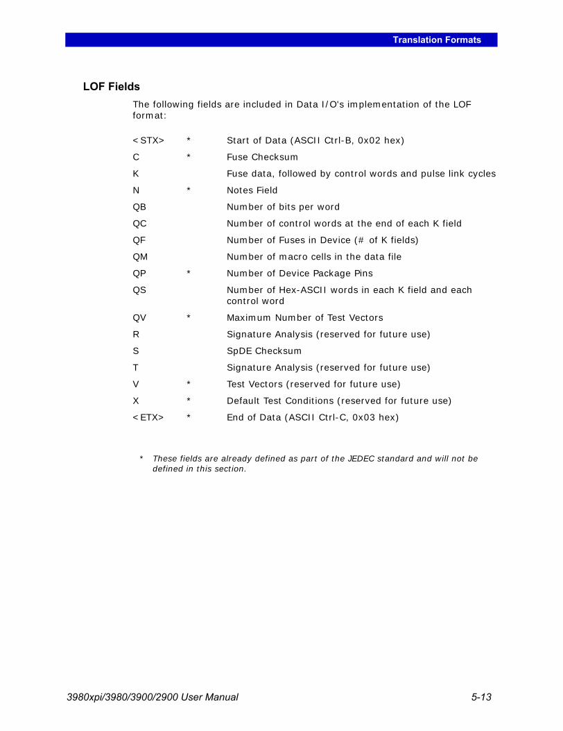
Translation Formats
3980xpi/3980/3900/2900 User Manual 5-13
LOF Fields The following fields are included in Data I/O's implementation of the LOF format:
* These fields are already defined as part of the JEDEC standard and will not be defined in this section.
<STX> * Start of Data (ASCII Ctrl-B, 0x02 hex)
C * Fuse Checksum
K Fuse data, followed by control words and pulse link cycles
N * Notes Field
QB Number of bits per word
QC Number of control words at the end of each K field
QF Number of Fuses in Device (# of K fields)
QM Number of macro cells in the data file
QP * Number of Device Package Pins
QS Number of Hex-ASCII words in each K field and each control word
QV * Maximum Number of Test Vectors
R Signature Analysis (reserved for future use)
S SpDE Checksum
T Signature Analysis (reserved for future use)
V * Test Vectors (reserved for future use)
X * Default Test Conditions (reserved for future use)
<ETX> * End of Data (ASCII Ctrl-C, 0x03 hex)

Translation Formats
5-14 3980xpi/3980/3900/2900 User Manual
ASCII Octal and Hex Formats, Codes 30-37 and 50-58Each of these formats has a start and end code, and similar address and checksum specifications. Figure 5-6 illustrates 4 data bytes coded in each of the 9 ASCII Octal and Hexadecimal formats. Data in these formats is organized into sequential bytes separated by the execute character (space, percent, apostrophe, or comma). Characters immediately preceding the execute character are interpreted as data. ASCII Octal and Hex formats can express 8-bit data, by 3 octal, or 2 hexadecimal characters. Line feeds, carriage returns, and other characters may be included in the data stream as long as a data byte directly precedes each execute character.
Figure 5-6. ASCII Octal and Hex Formats (example)
$A000000,377 377 377 377 377 377 377 377 377 377 377 377 377 377 377 377$S007760,
$A000000,377%377%377%377%377%377%377%377%377%377%377%377%377%377%377%377%$S007760,
$A000000,377'377'377'377'377'377'377'377'377'377'377'377'377'377'377'377'$S007760,
$A000000,377'377'377'377'377'377'377'377'377'377'377'377'377'377'377'377'$S007760,
$A0000,FF%FF%FF%FF%FF%FF%FF%FF%FF%FF%FF%FF%FF%FF%FF%FF%$S0FF0,
$A0000,FF FF FF FF FF FF FF FF FF FF FF FF FF FF FF FF$S0FF0,
$A0000,FF'FF'FF'FF'FF'FF'FF'FF'FF'FF'FF'FF'FF'FF'FF'FF'$S0FF0,
$A0000,FF,FF,FF,FF,FF,FF,FF,FF,FF,FF,FF,FF,FF,FF,FF,FF,$S0FF0,
$A0000,FF'FF'FF'FF'FF'FF'FF'FF'FF'FF'FF'FF'FF'FF'FF'FF'$S0FF0,
1
1
1
2
1
1
1
1
2
4
4
4
3
4
4
4
3
4
FORMAT 30 (OR 35)
FORMAT 31 (OR 36)
FORMAT 32
FORMAT 37
FORMAT 50 (OR 55)
FORMAT 51 (OR 56)
FORMAT 52
FORMAT 53 (OR 58)
FORMAT 57
Optional Octal Address Field (Typical)
Optional Octal Sumcheck Field (Typical)
Octal Data Byte (Typical)
Execute Character
Optional Hex Address Field
Optional Hex Sumcheck Field
LEGENDStart Code is nonprintable STX - CTRL B (optionally SOH - CTRL A)
Start Code is nonprintable SOM - CTRL R
End Code is nonprintable EOM - CTRL T
End Code is nonprintable ETX - CTRL C
1
2
3
4 0078-2

Translation Formats
3980xpi/3980/3900/2900 User Manual 5-15
Although each data byte has an address, most are implied. Data bytes are addressed sequentially unless an explicit address is included in the data stream. This address is preceded by a $ and an A, must contain 2 to 8 hex or 3 to 11 octal characters, and must be followed by a comma, except for the ASCII-Hex (Comma) format, which uses a period. The programmer skips to the new address to store the next data byte; succeeding bytes are again stored sequentially.
Each format has an end code, which terminates input operations. However, if a new start code follows within 16 characters of an end code, input will continue uninterrupted. If no characters come within 2 seconds, input operation is terminated.
After receiving the final end code following an input operation, the programmer calculates a sumcheck of all incoming data. Optionally, a sumcheck can also be entered in the input data stream. The programmer compares this sumcheck with its own calculated sumcheck. If they match, the programmer will display the sumcheck; if not, a sumcheck error will be displayed.
Note: The sumcheck field consists of either 2-4 hex or 3-6 octal characters, sandwiched between the $ and comma characters. The sumcheck immediately follows an end code. The sumcheck is optional in the input mode but is always included in the output mode. The most significant digit of the sumcheck may be 0 or 1 when expressing 16 bits as 6 octal characters.
The programmer divides the output data into 8-line blocks. Data transmission is begun with the start code, a nonprintable STX character, or optionally, SOH.* Data blocks follow, each one prefaced by an address for the first data byte in the block. The end of transmission is signaled by the end code, a nonprintable ETX character. Directly following the end code is a sumcheck of the transferred data.
* ASCII-Octal SMS and ASCII-Hex SMS use SOM (CTRL-R) as a start code and EOM (CTRL-T) as an end code.

Translation Formats
5-16 3980xpi/3980/3900/2900 User Manual
RCA Cosmac Format, Code 70Data in this format begins with a start record consisting of the start character (!M or ?M), an address field, and a space. See Figure 5-7.
The start character?M is sent to the programmer by a development system, followed by the starting address, and a data stream which conforms to the data input format described in the ASCII-Hex and Octal figure. Transmission stops when the specified number of bytes has been transmitted.
Address specification is required for only the first data byte in the transfer. An address must have 1 to 4 hex characters and must be followed by a space. The programmer records the next hexadecimal character after the space as the start of the first data byte. (A carriage return must follow the space if the start code ?M is used.) Succeeding bytes are recorded sequentially.
Each data record is followed by a comma if the next record is not preceded by an address, or by a semicolon if it starts with an address. Records consist of data bytes expressed as 2 hexadecimal characters and followed by either a comma or semicolon, and a carriage return. Any characters received between a comma or semicolon and a carriage return will be ignored by the programmer.
The carriage return character is significant to this format because it can signal either the continuation or the end of data flow; if the carriage return is preceded by a comma or semicolon, more data must follow; the absence of a comma or semicolon before the carriage return indicates the end of transmission.
Output data records are followed by either a comma or a semicolon and a carriage return. The start-of-file records are expressed exactly as for input.
Figure 5-7. RCA Cosmac Format (example)
!M0000 ,FFFFFFFFFFFFFFFFFFFFFFFFFFFFFFFF,FFFFFFFFFFFFFFFFFFFFFFFFFFFFFFFF,FFFFFFFFFFFFFFFFFFFFFFFFFFFFFFFF,FFFFFFFFFFFFFFFFFFFFFFFFFFFFFFFF,FFFFFFFFFFFFFFFFFFFFFFFFFFFFFFFF
Start Record!M or ?M = Start Characters0000 = Address
End-of-File Record
1
2
Data Records
FF =
, = ; =
2 Hex Characters = (1 Byte)Bytes per record is variableEnd of Record CharacterEnd of Record Characterif followed by expressedaddress
LEGEND
Nonprinting line feed, carriage return, and nulls
Nonprinting carriage return
1
20079-2

Translation Formats
3980xpi/3980/3900/2900 User Manual 5-17
Fairchild Fairbug, Code 80In the Fairbug format, input and output requirements are identical; both have 8-byte records and identical control characters. Figure 5-8 shows a Fairbug data file. A file begins with a 5-character prefix and ends with a 1-character suffix. The start-of-file character is an S, followed by the address of the first data byte. Each data byte is represented by 2 hexadecimal characters. The programmer will ignore all characters received prior to the first S.
Note: Address specification is optional in this format; a record with no address directly follows the previous record.
Each data record begins with an X and always contains 8 data bytes. A 1-digit hexadecimal checksum follows the data in each data record. The checksum represents, in hexadecimal notation, the sum of the binary equivalents of the 16 digits in the record; the half carry from the fourth bit is ignored.
The programmer ignores any character (except for address characters and the asterisk character, which terminates the data transfer) between a checksum and the start character of the next data record. This space can be used for comments.
The last record consists of an asterisk only, which indicates the end of file.
Figure 5-8. Fairchild Fairbug (example)
S0000XFFFFFFFFFFFFFFFFCXFFFFFFFFFFFFFFFFCXFFFFFFFFFFFFFFFFCXFFFFFFFFFFFFFFFFCXFFFFFFFFFFFFFFFFCXFFFFFFFFFFFFFFFFCXFFFFFFFFFFFFFFFFCXFFFFFFFFFFFFFFFFCXFFFFFFFFFFFFFFFFCXFFFFFFFFFFFFFFFFC*
Start RecordS = Start Character
0000 = Address Field
End-of-File Record
Data Records
X =
FF =
C =
Data Record Start Character
2 Hex Characters (1 Byte)
Checksum. 1-digit summation
of data in record
0080-2

Translation Formats
5-18 3980xpi/3980/3900/2900 User Manual
MOS Technology Format, Code 81The data in each record is sandwiched between a 7-character prefix and a 4-character suffix. The number of data bytes in each record must be indicated by the byte count in the prefix. The input file can be divided into records of various lengths.
Figure 5-9 shows a series of valid data records. Each data record begins with a semicolon. The programmer will ignore all characters received prior to the first semicolon. All other characters in a valid record must be valid hexadecimal digits (0-9 and A-F). A 2-digit byte count follows the start character. The byte count, expressed in hexadecimal digits, must equal the number of data bytes in the record. The byte count is greater than zero in the data records, and equals zero (00) in the end-of-file record. The next 4 digits make up the address of the first data byte in the record. Data bytes follow, each represented by 2 hexadecimal digits. The end-of-file record consists of the semicolon start character, followed by a 00 byte count, the record count, and a checksum.
The checksum, which follows each data record, is a 2-byte binary summation of the preceding bytes in the record (including the address and byte count), in hexadecimal notation.
Figure 5-9. MOS Technology Format (example)
;100000FFFFFFFFFFFFFFFFFFFFFFFFFFFFFFFF1000;100010FFFFFFFFFFFFFFFFFFFFFFFFFFFFFFFF1010;100020FFFFFFFFFFFFFFFFFFFFFFFFFFFFFFFF1020;100030FFFFFFFFFFFFFFFFFFFFFFFFFFFFFFFF1030;100040FFFFFFFFFFFFFFFFFFFFFFFFFFFFFFFF1040;0000050005
Sumcheck of record includingdata, address and byte count
Data Records
End-of-File Record
Record Count Sumcheck
Start Character
Byte Count
Address Field
LEGEND
Nonprinting Carriage Return, line feed,and nulls determined by null count 0081-2

Translation Formats
3980xpi/3980/3900/2900 User Manual 5-19
Motorola EXORciser Format, Code 82Motorola EXORciser data files may begin with an optional sign-on record, which is initiated by the start characters S0. Valid data records start with an 8-character prefix and end with a 2-character suffix. Figure 5-10 shows a series of valid Motorola data records.
Each data record begins with the start characters S1. The third and fourth characters represent the byte count, which expresses the number of data, address, and checksum bytes in the record. The address of the first data byte in the record is expressed by the last 4 characters of the prefix. Data bytes follow, each represented by 2 hexadecimal characters. The number of data bytes occurring must be three less than the byte count. The suffix is a 2-character checksum, which equals the one's complement of the binary summation of the byte count, address, and data bytes.
The end-of-file record consists of the start characters S9, the byte count, the address (in hex), and a checksum. The maximum record length is 250 data bytes.
Figure 5-10. Motorola EXORciser Format (example)
S1130000FFFFFFFFFFFFFFFFFFFFFFFFFFFFFFFFFC
S00B00004441544120492F4FF3
S1130010FFFFFFFFFFFFFFFFFFFFFFFFFFFFFFFFECS1130020FFFFFFFFFFFFFFFFFFFFFFFFFFFFFFFFDCS1130030FFFFFFFFFFFFFFFFFFFFFFFFFFFFFFFFCCS1130040FFFFFFFFFFFFFFFFFFFFFFFFFFFFFFFFBCS9030000FC
End-of-File RecordStart Character
Byte Count
Sumcheck
Address
End-of-File Record
Optional Sign-On Record(S0 = Sign-On Characters)
Byte Count + 3
Start Character
DataRecords
Sumcheckof record
LEGENDNonprinting Carriage Return, line feed, and nulls determined by null count 0082-2

Translation Formats
5-20 3980xpi/3980/3900/2900 User Manual
Intel Intellec 8/MDS Format, Code 83Intel data records begin with a 9-character prefix and end with a 2-character suffix. The byte count must equal the number of data bytes in the record.
Figure 5-11 simulates a series of valid data records. Each record begins with a colon, which is followed by a 2-character byte count. The 4 digits following the byte count give the address of the first data byte. Each data byte is represented by 2 hexadecimal digits; the number of data bytes in each record must equal the byte count. Following the data bytes of each record is the checksum, the two's complement (in binary) of the preceding bytes (including the byte count, address, record type and data bytes), expressed in hex.
The end-of-file record consists of the colon start character, the byte count (equal to 00), the address, the record type (equal to 01), and the checksum of the record.
Signetics Absolute Object Format, Code 85Figure 5-12 shows the specifications of Signetics format files. The data in each record are sandwiched between a 9-character prefix and a 2-character suffix.
Figure 5-11. Intel Intellec 8/MDS Format (example)
Figure 5-12. An Example of Signetics Absolute Object Format
:10000000FFFFFFFFFFFFFFFFFFFFFFFFFFFFFFFF00:10001000FFFFFFFFFFFFFFFFFFFFFFFFFFFFFFFFF0:10002000FFFFFFFFFFFFFFFFFFFFFFFFFFFFFFFFE0:10003000FFFFFFFFFFFFFFFFFFFFFFFFFFFFFFFFD0:10004000FFFFFFFFFFFFFFFFFFFFFFFFFFFFFFFFC0:00000001FF
Checksumof record
DataRecords
Byte Count Transmission Sumcheck
Record Type
End-of-File Record
2 Hex Characters (1 Byte)
Address
Start Character
0083-3
LEGENDNonprinting Carriage Return, line feed, and nulls determined by null count
:00001020FFFFFFFFFFFFFFFFFFFFFFFFFFFFFFFF00:00101060FFFFFFFFFFFFFFFFFFFFFFFFFFFFFFFF00:002010A0FFFFFFFFFFFFFFFFFFFFFFFFFFFFFFFF00:003010E0FFFFFFFFFFFFFFFFFFFFFFFFFFFFFFFF00:00401021FFFFFFFFFFFFFFFFFFFFFFFFFFFFFFFF00:000000
DataRecords
Data CheckStart Character
Address Check2 Hex Characters (1 Byte)
Byte Count (00 in End-of-File Record)Transfer Address
Nonprinting Carriage Return, line feeds, and nulls determined by null countLEGEND
0084-2

Translation Formats
3980xpi/3980/3900/2900 User Manual 5-21
The start character is a colon. This is followed by the address, the byte count, and a 2-digit address check. The address check is calculated by exclusive ORing every byte with the previous one, then rotating left one bit. Data are represented by pairs of hexadecimal characters. The byte count must equal the number of data bytes in the record. The suffix is a 2-character data check, calculated using the same operations described for the address check.
The end-of-file record consists of the colon start character, the address, and the byte count (equal to 00).
Tektronix Hexadecimal Format, Code 86Figure 5-13 illustrates a valid Tektronix data file. The data in each record are sandwiched between the start character (a slash) and a 2-character checksum. Following the start character, the next 4 characters of the prefix express the address of the first data byte. The address is followed by a byte count, which represents the number of data bytes in the record, and by a checksum of the address and byte count. Data bytes follow, represented by pairs of hexadecimal characters. Succeeding the data bytes is their checksum, an 8-bit sum, modulo 256, of the 4-bit hexadecimal values of the digits making up the data bytes. All records are followed by a carriage return.
Data are output from the programmer starting at the first RAM address and continuing until the number of bytes in the specified block has been transmitted. The programmer divides output data into records prefaced by a start character and an address field for the first byte in the record.
The end-of-file record consists of a start character (slash), followed by the transfer address, the byte count (equal to 00), and the checksum of the transfer address and byte count.
An optional abort record contains 2 start characters (slashes), followed by an arbitrary string of ASCII characters. Any characters between a carriage return and a / are ignored.
Figure 5-13. Tektronix Hex Format (example)
/00001001FFFFFFFFFFFFFFFFFFFFFFFFFFFFFFFFE0/00101002FFFFFFFFFFFFFFFFFFFFFFFFFFFFFFFFE0/00201003FFFFFFFFFFFFFFFFFFFFFFFFFFFFFFFFE0/00301004FFFFFFFFFFFFFFFFFFFFFFFFFFFFFFFFE0/00401005FFFFFFFFFFFFFFFFFFFFFFFFFFFFFFFFE0/00000000
DataRecords
Start Character Address Field
Byte Count(00 in End-of-File Record)
Transfer Address
Nonprinting Carriage Return, line feeds,and nulls determined by null count
LEGEND
0085-3
Checksum of Addressand Byte Count
Checksum ofData Bytes
End-of-File Record

Translation Formats
5-22 3980xpi/3980/3900/2900 User Manual
Motorola EXORmacs Format, Code 87Motorola data files may begin with an optional sign-on record, initiated by the start characters S0. Data records start with an 8- or 10-character prefix and end with a 2-character suffix. Figure 5-14 shows a series of Motorola EXORmacs data records.
Each data record begins with the start characters S1 or S2: S1 if the following address field has 4 characters, S2 if it has 6 characters. The third and fourth characters represent the byte count, which expresses the number of data, address, and checksum bytes in the record. The address of the first data byte in the record is expressed by the last 4 characters of the prefix (6 characters for addresses above hexadecimal FFFF). Data bytes follow, each represented by 2 hexadecimal characters. The number of data bytes occurring must be 3 or 4 less than the byte count. The suffix is a 2-character checksum, the one's complement (in binary) of the preceding bytes in the record, including the byte count, address, and data bytes.
The end-of-file record begins with an S9 start character. Following the start characters are the byte count, the address, and a checksum. The maximum record length is 250 data bytes.
Figure 5-14. Motorola EXORmacs Format (example)
S214FF0000FFFFFFFFFFFFFFFFFFFFFFFFFFFFFFFFFC
S00B00004441544120492F4FF3
S1130010FFFFFFFFFFFFFFFFFFFFFFFFFFFFFFFFECS1130020FFFFFFFFFFFFFFFFFFFFFFFFFFFFFFFFDCS1130030FFFFFFFFFFFFFFFFFFFFFFFFFFFFFFFFCCS1130040FFFFFFFFFFFFFFFFFFFFFFFFFFFFFFFFBCS9030000FC
StartCharacter
Byte Count
Checksum
Address
End-of-File Record
Optional Sign-On Record
DataRecords
LEGENDNonprinting Carriage Return, line feed, and nulls determined by null count 0086-3
Checksum
Checksum

Translation Formats
3980xpi/3980/3900/2900 User Manual 5-23
Intel MCS-86 Hexadecimal Object, Code 88The Intel 16-bit Hexadecimal Object file record format has a 9-character (4-field) prefix that defines the start of record, byte count, load address, and record type and a 2-character checksum suffix. Figure 5-15 shows a sample record of this format.
The four record types are described below.
00 — Data RecordThis begins with the colon start character, which is followed by the byte count (in hex notation), the address of the first data byte, and the record type (equal to 00). Following these are the data bytes. The checksum follows the data bytes and is the two's complement (in binary) of the preceding bytes in the record, including the byte count, address, record type, and data bytes.
01 — End RecordThis end-of-file record also begins with the colon start character. This is followed by the byte count (equal to 00), the address (equal to 0000), the record type (equal to 01), and the checksum, FF.
02 — Extended Segment Address RecordThis is added to the offset to determine the absolute destination address. The address field for this record must contain ASCII zeros (Hex 30s). This record type defines bits 4 to 19 of the segment base address. It can appear randomly anywhere within the object file and affects the absolute memory address of subsequent data records in the file. The following example illustrates how the extended segment address is used to determine a byte address.
Figure 5-15. Intel MCS-86 Hex Object (example)
:10000000FFFFFFFFFFFFFFFFFFFFFFFFFFFFFFFF00:10001000FFFFFFFFFFFFFFFFFFFFFFFFFFFFFFFFF0:10002000FFFFFFFFFFFFFFFFFFFFFFFFFFFFFFFFE0:10003000FFFFFFFFFFFFFFFFFFFFFFFFFFFFFFFFD0:10004000FFFFFFFFFFFFFFFFFFFFFFFFFFFFFFFFC0:00000001FF
DataRecords
Byte Count ChecksumRecord Type
End-of-File Record
AddressStart Character
0087-4
LEGENDNonprinting Carriage Return, line feed, and nulls determined by null count
:020000020000FC Extended Record
Offset Address
ChecksumChecksum

Translation Formats
5-24 3980xpi/3980/3900/2900 User Manual
Problem:
Find the address for the first data byte for the following file.
: 02 0000 02 1230 BA : 10 0045 00 55AA FF .....BC
Solution:
Step 1. Find the record address for the byte. The first data byte is 55.Its record address is 0045 from above.
Step 2. Find the offset address. The offset address is 1230 from above.
Step 3. Shift the offset address one place left, then add it to the record address, like this:
The address for the first data byte is 12345.
Note: Always specify the address offset when using this format, even when the offset is zero.
During output translation, the firmware will force the record size to 16 (decimal) if the record size is specified greater than 16. There is no such limitation for record sizes specified less than 16.
03 — Start RecordThis record type is not sent during output by Data I/O translator firmware.
1230 Offset address (upper 16 bits)+ 0045 Record address (lower 16 bits)
12345 20-bit address

Translation Formats
3980xpi/3980/3900/2900 User Manual 5-25
Hewlett-Packard 64000 Absolute Format, Code 89Hewlett-Packard Absolute is a binary format with control and data-checking characters. See Figure 5-16.
Data files begin with a Start-of-file record, which includes the Data Bus Width, Data Width Base, Transfer Address, and a checksum of the bytes in the record.
The Data Bus Width represents the width of the target system's bus (in bits). The Data Width Base represents the smallest addressable entity used by the target microprocessor.
Figure 5-16. HP 64000 Absolute Format (example)
End-of-File record consists only of a word count of 0.
Checksum
Data bytes
Address where following data byte is to be stored.
BYTE COUNT — number of 8-bit data bytes.WORD COUNT — number of 16-bit words in record except checksum and itself.CHECKSUM — modulo 256 sum of all bytes in the record except the first byte.
TRANSFER ADDRESS — for microprocessor program counter.
DATA WIDTH BASE — see text.
DATA BUS WIDTH — see text.WORD COUNT — number of 16-bit words in the record; always 04 in Start-of-File record.
Note:
START-OF-FILERECORD
ONE DATARECORD
END-OF-FILERECORD
0088-2
HIGHORDER
LOWORDER
Third ByteMSBLSBSecond Byte
32-bit addressis sent in thismanner, in 4groups of 8-bitbytes.
This format is binary. Therefore, no ASCII control charactersor carriage returns and line feeds are allowed.
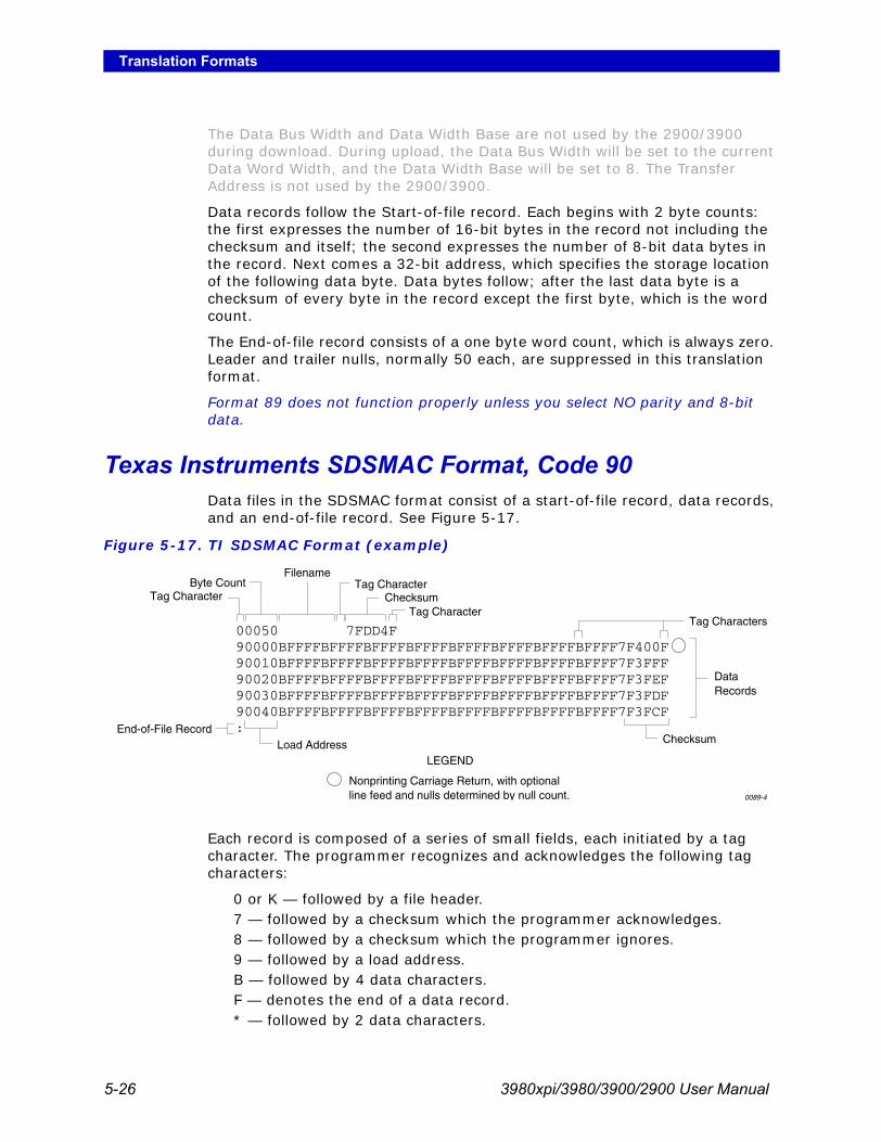
Translation Formats
5-26 3980xpi/3980/3900/2900 User Manual
The Data Bus Width and Data Width Base are not used by the 2900/3900 during download. During upload, the Data Bus Width will be set to the current Data Word Width, and the Data Width Base will be set to 8. The Transfer Address is not used by the 2900/3900.
Data records follow the Start-of-file record. Each begins with 2 byte counts: the first expresses the number of 16-bit bytes in the record not including the checksum and itself; the second expresses the number of 8-bit data bytes in the record. Next comes a 32-bit address, which specifies the storage location of the following data byte. Data bytes follow; after the last data byte is a checksum of every byte in the record except the first byte, which is the word count.
The End-of-file record consists of a one byte word count, which is always zero. Leader and trailer nulls, normally 50 each, are suppressed in this translation format.
Format 89 does not function properly unless you select NO parity and 8-bit data.
Texas Instruments SDSMAC Format, Code 90Data files in the SDSMAC format consist of a start-of-file record, data records, and an end-of-file record. See Figure 5-17.
Each record is composed of a series of small fields, each initiated by a tag character. The programmer recognizes and acknowledges the following tag characters:
0 or K — followed by a file header.7 — followed by a checksum which the programmer acknowledges.8 — followed by a checksum which the programmer ignores.9 — followed by a load address.B — followed by 4 data characters.F — denotes the end of a data record.* — followed by 2 data characters.
Figure 5-17. TI SDSMAC Format (example)
00050 7FDD4F90000BFFFFBFFFFBFFFFBFFFFBFFFFBFFFFBFFFFBFFFF7F400F90010BFFFFBFFFFBFFFFBFFFFBFFFFBFFFFBFFFFBFFFF7F3FFF90020BFFFFBFFFFBFFFFBFFFFBFFFFBFFFFBFFFFBFFFF7F3FEF90030BFFFFBFFFFBFFFFBFFFFBFFFFBFFFFBFFFFBFFFF7F3FDF90040BFFFFBFFFFBFFFFBFFFFBFFFFBFFFFBFFFFBFFFF7F3FCF:
ChecksumTag Character
Tag CharacterTag Character
Byte CountFilename
Load AddressEnd-of-File Record
Tag Characters
DataRecords
Checksum
LEGEND
Nonprinting Carriage Return, with optionalline feed and nulls determined by null count. 0089-4

Translation Formats
3980xpi/3980/3900/2900 User Manual 5-27
The start-of-file record begins with a tag character and a 12-character file header. The first four characters are the byte count of the data bytes; the remaining file header characters are the name of the file and may be any ASCII characters (in hex notation). Next come interspersed address fields and data fields (each with tag characters). If any data fields appear before the first address field in the file, the first of those data fields is assigned to address 0000. Address fields may be expressed for any data byte, but none are required.
The record ends with a checksum field initiated by the tag character 7 or 8, a 4-character checksum, and the tag character F. The checksum is the two's complement of the sum of the 8-bit ASCII values of the characters, beginning with the first tag character and ending with the checksum tag character (7 or 8).
Data records follow the same format as the start-of-file record but do not contain a file header. The end-of-file record consists of a colon (:) only. The output translator sends a CTRL-S after the colon.
JEDEC Format, Codes 91 and 92The JEDEC (Joint Electron Device Engineering Council) format is used to transfer fuse and test vector data between the programmer and a host computer. Code 91 is full format, and includes all the data fields (such as note and test fields) described on the following pages. Code 92 is the Kernel, or shorter, format. The JEDEC Kernel format includes only the minimum information needed for the programming; it does not, for example, include information fields or test vector fields. Prior to transferring a JEDEC file, the appropriate Logic device must be selected.
JEDEC's legal character set consists of all the printable ASCII characters and four control characters. The four allowable control characters are STX, ETX, CR (RETURN), and LF (line feed). Other control characters, such as ESC or BREAK, should not be used.
Note: This is Data I/O Corporation's implementation of JEDEC Standard 3A. For a copy of the strict standard, write to:
Electronic Industries AssociationEngineering Department2001 Eye Street NWWashington, D.C. 20006

Translation Formats
5-28 3980xpi/3980/3900/2900 User Manual
BNF Rules and Standard DefinitionsThe Backus-Naur Form (BNF) is used in the description here to define the syntax of the JEDEC format. BNF is a shorthand notation that follows these rules:
:: = denotes “is defined as.”
Characters enclosed by single quotes are literals (required).
Angle brackets enclose identifiers.
Square brackets enclose optional items.
Braces enclose a repeated item. The item may appear zero or more times.
Vertical bars indicate a choice between items.
Repeat counts are given by a :n suffix. For example, a 6-digit number would be defined as:
<number< :: = <digit>:6
For example, in words, the definition of a person's name reads:
The full name consists of an optional title followed by a first name, a middle name, and a last name. The person may not have a middle name or may have several middle names. The titles consist of: Mr., Mrs., Ms., Miss, and Dr.
The BNF definition for a person's name is:
<full name> :: = [<title>] <f. name> <m.name> <l. name>
<title> :: = 'Mr.' | 'Mrs.' | 'Ms.' | 'Miss' | 'Dr.'
The following standard definitions are used throughout the rest of this document:
<digit> :: = '0' | '1' | '2' | '3' | '4' | '5' | '6' | '7' | '8' | '9'
<hex-digit> :: = <digit> | 'A' | 'B' | 'C' | 'D' | 'E' | 'F'
<binary-digit> :: = '0' | '1'
<number> :: = <digit> <digit>
<del> :: = <space> | <carriage return>
<delimiter> :: = <del> <del>
<printable character> :: = <ASCII 20 hex ... 7E hex>
<control character> :: = <ASCII 00 hex ... 1F hex> | <ASCII 7F hex>
<STX> :: = <ASCII 02 hex>
<ETX> :: = <ASCII 03 hex>
<carriage return> :: = <ASCII 0D hex>
<line feed> :: = <ASCII 0A hex>
<space> :: = <ASCII 20 hex> | ' '
<valid character> :: = <printable character> | <carriage return> | <line feed>
<field character> :: = <ASCII 20 hex ... 29 hex> | <ASCII 2B hex ... 7E hex> | <carriage return> | <line feed>

Translation Formats
3980xpi/3980/3900/2900 User Manual 5-29
The Design Specification Field<design spec> ::= <field character>`*'
The first field sent in a JEDEC transmission is the design specification. Both the full and kernel JEDEC formats accept the design specification field. This field is mandatory and does not have an identifier (such as an asterisk) signaling its beginning. The design specification field consists of general device information. It could, for example, consist of the following information: your name, your company's name, the date, the device name and manufacturer, design revision level, etc. This field is terminated by an asterisk character. Examine the sample transmission shown on the next page of this description — the first three lines of the file comprise the design specification field. The programmer ignores the contents of this field for downloads and places “Data I/O” in this field for upload operations.
Note: You do not need to send any information in this field if you do not wish to; a blank field, consisting of the terminating asterisk, is a valid design specification field.
The Transmission Checksum Field<xmit checksum> ::= <hex digit>:4
The transmission checksum is the last value sent in a JEDEC transmission. The full JEDEC format requires the transmission checksum. The checksum is a 16-bit value, sent as a 4-digit hex number, and is the sum of all the ASCII characters transmitted between (and including) the STX and ETX. The parity bit is excluded in the calculation of the transmission checksum.
Some computer systems do not allow you to control what characters are sent, especially at the end of a line. You should set up the equipment so that it will accept a dummy value of 0000 as a valid checksum. This zero checksum is a way of disabling the transmission checksum, while still keeping within the JEDEC format rules.

Translation Formats
5-30 3980xpi/3980/3900/2900 User Manual
JEDEC Full Format, Code 91 The full JEDEC format consists of a start-of-text character (STX), various fields, an end-of-text character (ETX), and a transmission checksum. A sample JEDEC transmission sent in the full format is shown in Figure 5-18. Each of the fields is described on the following pages.
Figure 5-18. JEDEC Full Format (example)
ABEL(tm) Version 2.00b JEDEC file for:P20R8Large Memory Version
Created on: 09-Mar-87 04:45 PM8-bit barrel shifterEngineerI Data I/O Corp Redmond WA 10 Jan 1986*QP24* QF2560*L0000110111111111111111111111111110111011101011011111111111111111111110111111101110011101111111111111111110111111111110110110110111111111111110111111111111111011010111011111111110111111111111111111011110101101111110111111111111111111111101111001100110111111111111111111111111110111011010011111111111111111111111111111011101011001111111111111111111111111101101110101110111111111111111111111111110111011101011011111111111111111111110111111101110011101111111111111111110111111111110110110110111111111111110111111111111111011010111011111111110111111111111111111011110101101111110111111111111111111111101111001100110111111111111111111111111110111011010011111111111111111111111111111011101011001111111111111111111111111101101110101*V0001 C1000000000N00HLLLLLLL1N*V0002 C1000000000N01LHLLLLLL1N*V0003 C1000000001N00LLHLLLLL1N*V0004 C1000000001N01LLLHLLLL1N*V0005 C1000000010N00LLLLHLLL1N*V0006 C1000000010N01LLLLLHLL1N*V0007 C1000000011N00LLLLLLHL1N*V0008 C1000000011N01LLLLLLLH1N*V0009 C0111111100N00LHHHHHHH1N*V0010 C0111111100N01HLHHHHHH1N*V0011 C0111111101N00HHLHHHHH1N*V0012 C0111111101N01HHHLHHHH1N*V0013 C0111111110N00HHHHLHHH1N*V0014 C0111111110N01HHHHHLHH1N*V0015 C0111111111N00HHHHHHLH1N*V0016 C0111111111N01HHHHHHHL1N*V0017 C0000000100N01HLLLLLLL1N*V0018 C1111111000N01LHHHHHHH1N*V0019 C0000000000N00HHHHHHHH0N*V0020 C0000000000N10ZZZZZZZZ1N*C1B20*B8C0
Header(comment area -everythingpreceedingfirst * isignored)
Number of Pins (24)and Number of Fuses (2560)
Fuse Address (0000)
Fuse States:0 = intact1 = blown
Test Vectors
Fuse Map ChecksumTransmission Checksum 0090-3
VectorNumber

Translation Formats
3980xpi/3980/3900/2900 User Manual 5-31
JEDEC Field Syntax<field> ::= [<delimiter>]<field identifier><field character>`*'
<field identifier>::= 'A' | 'C' | 'D' | 'F' | 'G' | 'K' | 'L' | 'N' | 'P' | 'Q' | 'R' | 'S' | 'T' | 'V' | 'X'
<reserved identifier>::= 'B' | 'E' | 'H' | 'I' | 'J' | 'M' | 'O' | 'U' | 'W' | 'Y' | 'Z'
Following the design specification field in a JEDEC transmission can be any number of information fields. Each of the JEDEC fields begins with a character that identifies what type of field it is. Fields are terminated by using an asterisk character. Multiple character identifiers can be used to create sub-fields (i.e., A1, A$, or AB3). Although they are not required, you may use carriage returns (CR) and line feeds (LF) to improve readability of the data.
Field IdentifiersField identifiers which are currently used in JEDEC transmissions are shown above on the “field identifiers” line. The “reserved identifier” line indicates characters not currently used (reserved for future use as field identifiers). JEDEC field identifiers are defined as follows:
* Reserved for future use
Device Field (D)Device selection by this field is not supported by the programmer. It has been replaced by the QF and QP fields and manual selection of devices.
A Access time N Note field
B * O *
C Checksum field P Pin sequence
D Device type Q Value field
E * R Resulting vector field
F Default fuse state field S Starting vector
G Security fuse field T Test cycles
H * U *
I * V Test vector field
J * W *
K Fuse list field (hex format) X default test condition
L Fuse list field Y *
M * Z *

Translation Formats
5-32 3980xpi/3980/3900/2900 User Manual
Fuse Information Fields (L, K, F, C)<fuse information> :: = [<default state>] <fuse list> <fuse list> [<fuse checksum>]
<fuse list> : = 'L' <number> <delimiter> <binary-digit> [<delimiter>] ' * '
<fuse list> :: = 'K' <number> <delimiter> <hex-digit> [<delimiter>] '*'
<default state> :: = 'F' <binary-digit> ' * '
<fuse checksum> :: = 'C' <hex-digit>:4 ' * '
Each fuse of a device is assigned a decimal number and has two possible states: zero, specifying a low-resistance link, or one, specifying a high resistance link. The state of each fuse in the device is given by three fields: the fuse list (L field or K field), the default state (F field), and the fuse checksum (C field).
Fuse states are explicitly defined by either the L field or the K field. The character L begins the L field and is followed by the decimal number of the first fuse for which this field defines a state. The first fuse number is followed by a list of binary values indicating the fuse states.
The information in the K field is the same as that of the L field except that the information is represented by hex characters instead of binary values. This allows more compact representation of the fusemap data. The character K begins the K field and is followed by the decimal number of the first fuse. The fuse data follow the fuse number and are represented by hex characters. Each bit of each hex character represents the state of one fuse, so each hex character represents four fuses. The most significant bit of the first hex character following the fuse number corresponds to the state of that fuse number. The next most significant bit corresponds to the state of the next fuse number, etc. The least significant bit of the first hex character corresponds to the state of the fuse at the location specified by the fuse number plus three.
The K field supports download operations only. The K field is not part of the JEDEC standard, but is supported by Data I/O for fast data transfer. The L and K fields can be any length desired, and any number of L or K fields can be specified. If the state of a fuse is specified more than once, the last state specified replaces all previous ones for that fuse. The F field defines the states of fuses that are not explicitly defined in the L or K fields. If no F field is specified, all fuse states must be defined by L or K fields.
The C field, the fuse information checksum field, is used to detect transmitting and receiving errors. The field contains a 16-bit sum (modulus 65535) computed by adding 8-bit words containing the fuse states for the entire device. The 8-bit words are formed as shown in the following figure. Unused bits in the final 8-bit word are set to zero before the checksum is calculated.
Word 00 | msb | | | | | | | lsb |
Fuse No. 7 6 5 4 3 2 1 0
Word 01 | msb | | | | | | | lsb |
Fuse No. 15 14 13 12 11 10 9 8
Word 62 | msb | | | | | | | lsb |
Fuse No. 503 - - - 499 498 497 496

Translation Formats
3980xpi/3980/3900/2900 User Manual 5-33
Following is an example of full specification of the L, C, and F fields:
F0*L0 01010101* L0008 01010111* L1000 0101*C019E*
Following is an alternate way of defining the same fuse states using the K field:
F0*K0 55* K0008 57* K1000 5* C019E*
Another example, where F and C are not specified:
L0200 01101010101010101011
010111010110100010010010010*
The Security Fuse Field (G) <security fuse>::=`G'<binary-digit>`*'
The JEDEC G field is used to enable the security fuse of some logic devices. To enable the fuse, send a 1 in the G field:
G1*
The Note Field (N)<note>::=`N'<field characters>`*'
The note field is used in JEDEC transmission to insert notes or comments. The programmer will ignore this field; it will not be interpreted as data. An example of a note field would be:
N Test Preload*
The Value Fields (QF, QP, and QV)
JEDEC value fields define values or limits for the data file, such as number of fuses. The QF subfield defines the number of fuses in the device. All of the value fields must occur before any device programming or testing fields appear in the data file. Files with ONLY testing fields do not require the QF field and fields with ONLY programming data do not require the QP and QV fields.
The QF subfield tells the programmer how much memory to reserve for fuse data, the number of fuses to set to the default condition, and the number of fuses to include in the fuse checksum. The QP subfield defines the number of pins or test conditions in the test vector, and the QV subfield defines the maximum number of test vectors.
The P FieldThe P field remaps the device pinout and is used with the V (test vector) field. An asterisk terminates the field. The syntax of the field is as follows:
<pin<N>list>::='P'<pin number>:N'*'
<pin<N>number>::=<delimiter><number>

Translation Formats
5-34 3980xpi/3980/3900/2900 User Manual
The following example shows a P field, V field, and the resulting application:
P 1 2 3 4 5 6 14 15 16 17 7 8 9 10 11 12 13 18 19 20 *
V0001 111000HLHHNNNNNNNNNN*
V0002 100000HHHLNNNNNNNNNN*
The result of applying the above P and V fields is that vector 1 will apply 111000 to pins 1 through 6, and HLHH to pins 14 through 17. Pins 7 through 13 and 18 through 20 will not be tested.
JEDEC U and E FieldsAs of Version 2.5, the programmer supports the optional JEDEC U (user data) and E (electrical data) fields. The U and E fields are described below.
Note: Implementation of the JEDEC U and E fields is not part of the JEDEC-3C (JESD3-C) standard.
User Data (U Field)The U field allows user data fuses that do not affect the logical or electrical functionality of the device to be specified in JEDEC files. For instance, the U field can be used to specify the User Data Signature fuse available in some types of PLD devices because this fuse contains information only (it has no logical or electrical functionality).
Note: To have the JEDEC U field processed correctly, you must select the device before downloading the JEDEC file.
The following guidelines apply to the U field:
The U field must be included for devices with U fuses. Each U-field cell must be explicitly provided if the U field is present.The F (default fuse state) field does not affect U fuses.
There can only be one U field in a JEDEC file.The U field fuses must be listed in the order they appear in the device.The U field must be listed after the L field and E fields (if used), and before the V (test vector) field (if used).The U field is specified using binary numbers, since the full number of U-field cells is otherwise unknown. The number of cells specified in the U field is not included in the QF (number of fuses) field. The U-field cells are not included in the C (fuse checksum) field. The U field reads left to right to be consistent with the L (fuse list) and E fields.
The syntax for the U field is as follows:
<User Data Fuse List>::'U'<binary-digit(s)>'*'
The character U begins the U field and is followed by one binary digit for each U fuse. Each binary digit indicates one of two possible states (zero, specifying a low-resistance link, or one, specifying a high-resistance link) for each fuse.

Translation Formats
3980xpi/3980/3900/2900 User Manual 5-35
For example,
QF24*L0000101011000000000000000000*E10100111*C011A*U10110110*
Electrical Data (E field)The E field allows special feature fuses that do not affect the logic function of the device to be specified in JEDEC files.
The following guidelines apply to the E field:
The E-field cell must be explicitly provided if the E field is present.The F (default fuse state) field does not affect E fuses. There can only be one E field in a JEDEC file.The E field fuses must be listed in the order they appear in the device.The E field must be listed before the C (checksum) field. If the U field is used, the E field must come before the U (user data) field.The E field is specified using binary numbers, since the full number of E-field cells is otherwise unknown.The number of cells specified in the E field is not included in the QF (number of fuses) field. The E-field cells are included in the C (fuse checksum) field. The E field reads left to right for the purpose of checksum calculation.
The syntax for the E field is as follows:
<Electrical Data Fuse List>::'E'<binary digit(s)>'*'
The character E begins the E field and is followed by one binary digit for each E fuse. Each binary digit indicates one of two possible states (zero, specifying a low-resistance link, or one, specifying a high-resistance link) for each fuse. For example,
QF24*L0000101011000000000000000000*E10100111*C011A*U10110110*
Test Field (V field)<function test> :: = [<pin list>] <test vector> <test vector>
<pin<N>number> :: = <delimiter> <number>
N :: = number of pins on device
<test vector> :: = 'V' <number> <delimiter> < test condition> :N ' * '
<test condition> :: = <digit> 'B' | 'C' | 'D' | 'F' | 'H' | 'K' | 'L' | 'N' | 'P' | 'U' | 'X' | 'Z'
<reserved condition> :: = 'A' | 'E' | 'G' | 'I' | 'J' | 'M' | 'O' | 'Q' | 'R' | 'S' | 'T' | 'V' | 'W' | 'Y' | 'Z'

Translation Formats
5-36 3980xpi/3980/3900/2900 User Manual
Functional test information is specified by test vectors containing test conditions for each device pin. Each test vector contains n test conditions where n is the number of pins on the device. The following table lists the conditions that can be specified for device pins.
When using structured test vectors to check your logic design, do NOT use 101 or 010 transitions as tests for clock pins: use C, K, U, or D instead.
Test Conditions
Note: C, K, U, and D are clocking functions that allow for setup time.
The C, K, U, and D driving signals are presented after the other inputs are stable. The L, H, and Z tests are performed after all inputs have stabilized, including C, K, U, and D.
Test vectors are numbered by following the V character with a number. The vectors are applied in numerical order. If the same numbered vector is specified more than one time, the data in the last vector replaces any data contained in previous vectors with that number.
The following example uses the V field to specify functional test information for a device:
V0001 C01010101NHLLLHHLHLN *
V0002 C01011111NHLLHLLLHLN *
V0003 C10010111NZZZZZZZZZN *
V0004 C01010100NFLHHLFFLLN *
0 Drive input low1 Drive input high2-9 Drive input to supervoltage #2-9B Buried register preload (not supported)C Drive input low, high, lowD Drive input low, fast slewF Float input or outputH Test output highK Drive input high, low, highL Verifies that the specified output pin is lowN Power pins and outputs not testedP Preload registersU Drive input high, fast slewX Output not tested, input default levelZ Test input or output for high impedance

Translation Formats
3980xpi/3980/3900/2900 User Manual 5-37
JEDEC Kernel Mode, Code 92<kernel>::=<STX><design spec><min. fuse information><ETX><xmit checksum>
<design spec>::=<field character>`*'
<min. fuse information>::=<fuse list><fuse list>
You may use the JEDEC kernel format if you wish to send only the minimum data necessary to program the logic device, for example, if you do not want to send any test vectors. If you specify format code 92, the programmer will ignore everything except the design specification field and the fuse information field. The following fields will be ignored if format 92 is specified: C, F, G, Q, V, and X. Also, the security fuse will be set to zero and the transmission checksum will be ignored.
Figure 5-19 shows an example of a kernel JEDEC transmission.
Extended Tektronix Hexadecimal Format, Code 94The Extended Tektronix Hexadecimal format has three types of records: data, symbol, and termination records. The data record contains the object code. Information about a program section is contained in the symbol record (the programmer ignores symbol records), and the termination record signifies the end of a module. The data record (see sample below) contains a header field, a load address, and the object code. Figure 5-20 lists the information contained in the header field.
Figure 5-19. JEDEC Kernel Mode Format (example)
Figure 5-20. An Example of Tektronix Extended Format
<STX>Acme Logic Design Jane Engineer Feb. 29 1983Widget Decode 756-AB-3456 Rev C Device Mullard 12AX7*
L0000 1111111011 1111111111 1111000000 00000000000000000000 0000000000 0000000000 00000000000000000000 0000000101 1111111111 11111111110000000000 0000000000 0000111101 11111111111111111111 1111110111 1111111111 1111111111*
L0200 1110101111 1111110000 0000000000 00000000001111111111 1111011011 1111111111 11111111100111111111 1111111111 1111111110 11111111111111111111 1111101111 1111111111 11111011110000000000 0000000000 0000*
<EXT>0000 0091-2
%1561C310020202020202
SUMCHECK: 1CH = 1+5+6+3+1+0+0+0+2+0+2+...
OBJECT CODE: 6 BYTES
LOAD ADDRESS: 100 H
BLOCK TYPE: 6 (DATA)
HEADER CHARACTER
BLOCK LENGTH: 15H = 21
0092-2

Translation Formats
5-38 3980xpi/3980/3900/2900 User Manual
Character Values for Checksum ComputationThe number of fields in the file will vary, depending on whether a data or a termination block is sent. Both data and termination blocks have a 6-character header and a 2-to-17 character address.
The load address determines where the object code will be located. This is a variable length number that may contain up to 17 characters. The first number determines the address length, with a zero signifying a length of 16. The remaining characters of the data record contain the object code, 2 characters per byte.
When you copy data to the port or to RAM, set the high-order address if the low-order is not at the default value.
ItemNo. of ASCII Characters Description
% 1 Signifies that the record is the Extended Tek Hex format.
Block length 2 Number of characters in the record, minus the %.
Block type 1 6 = data record3 = symbol record (ignored by the
programmer)8 = termination record
Checksum 2 A 2-digit hex sum, modulo 256, of all the values in the record except the % and the checksum.
Character(s) Value (decimal) Character(s) Value (decimal)
0 . . 9 0 . . 9 . (period) 38
A . . Z 10 . . 35 _(underline) 39
$ 36 a . . z 40 . . 65
% 37

Translation Formats
3980xpi/3980/3900/2900 User Manual 5-39
Motorola 32-Bit Format, Code 95The Motorola 32-bit format closely resembles the Motorola EXORmacs format, the main difference being the addition of the S3 and S7 start characters. The S3 character is used to begin a record containing a 4-byte address. The S7 character is a termination record for a block of S3 records. The address field for an S7 record may optionally contain the 4-byte instruction address that identifies where control is to be passed and is ignored by the programmer. Figure 5-21 shows a sample of the Motorola 32-bit format.
Motorola data files may begin with an optional sign-on record, initiated by the start characters S0 or S5. Data records start with an 8- or 10-character prefix and end with a 2-character suffix.
Each data record begins with the start characters S1, S2, or S3: S1 if the following address field has 4 characters, S2 if it has 6 characters, S3 if it has 8 characters. The third and fourth characters represent the byte count, which expresses the number of data, address, and checksum bytes in the record. The address of the first data byte in the record is expressed by the last 4 characters of the prefix (6 characters for addresses above hexadecimal FFFF and 8 characters for addresses above hexadecimal FFFFFF). Data bytes follow, each represented by 2 hexadecimal characters. The number of data bytes occurring must be 3, 4, or 5 less than the byte count. The suffix is a 2-character checksum, the one's complement (in binary) of the preceding bytes in the record, including the byte count, address, and data bytes.
The end-of-file record begins with an S8 or S9 start character. Following the start characters are the byte count, the address, and a checksum. The maximum record length is 250 data bytes.
Figure 5-21. Motorola S3 Format (example)
S00B00004441544120492F4FF3S31500000000AA55AA55AA55AA55AA55AA55AA55AA55F2S30D00000010AA55AA55AA55AA55E6S70500000000FA
StartCharacter
Byte Count AddressChecksum
Optional Sign-On Record
Data Records0093-4
MSBLSB

Translation Formats
5-40 3980xpi/3980/3900/2900 User Manual
Hewlett-Packard UNIX Format, Code 96This format divides the data file into data records; each with a maximum size of 250 bytes not including header information. An ID header is added to the beginning of the first record. Each subsequent record has its own header section. The section at the beginning of the file contains the following elements: the header 8004, filename, byte count for the processor information record, and the processor information record.
The header 8004 identifies the type of file being transferred. The first byte of this header (80) indicates that this file is binary and the 04 indicates the type of file (absolute).
The ID header is followed by a 16-byte filename (not used by the programmer).
Next is the byte count, which indicates the size (minus one) of the Processor Information Record that follows. The Processor Information Record is divided into the following data words: Data Bus Width, Data Width Base, Transfer Address LS (least significant), and Transfer Address MS (most significant).
The Data Bus Width represents the width of the target system's bus (in bits). The Data Width Base represents the smallest addressable entity used by the target microprocessor.
The Data Bus Width and Data Width Base are not used by the programmer during download. During upload, the Data Bus Width will be set to the current Data Word Width, and the Data Width Base will be set to 8. The Transfer Address LS and Transfer Address MS are not used by the programmer.
The data records consist of a header (8 bytes) and the data bytes. The first 2 bytes of the header indicate the size of the data record including the header (minus one). If the number of data bytes in the data record (not including the header) is odd, one extra byte will be added to the data record to ensure that an even number of data bytes exist in the data record. The maximum value for this field is 00FF hex. The next two bytes indicate the number of actual data bytes in the record, not including the header bytes and the extra byte (if present). The maximum value for this field is 00FA hex. The 4 bytes that follow represent the destination address for the data in this record. The rest of the bytes in the record are the data bytes.
This format has no end of file identifier.

Translation Formats
3980xpi/3980/3900/2900 User Manual 5-41
The record length during upload is not affected by the upload record size parameter in the Configure/Edit/Communication screen. It is automatically set to transfer records using the maximum size (250 bytes), except for the last record. The size of the last record will be set according to the remaining number of data bytes.
Intel OMF386 Format, Code 97This data translation format is considered by Intel to be proprietary information. Contact your local Intel representative or call (408) 987-8080 for information about the structure of this format.
Figure 5-22. Hewlett-Packard 64000 Unix Format
80 04 20 20 20 20 20 20-20 20 20 20 20 20 20 2020 20 00 07 00 08 00 08-00 00 00 00 00 FF 00 FA00 00 00 00 02 00 26 02-03 38 FF FF FF FF FF 0230 38 FF FF FF FF FF 02-03 38 FF FF FF FF FF 0203 38 FF FF FF FF FF 02-03 16 75 A8 00 75 82 1075 D0 00 75 B8 10 75 89-20 75 88 40 75 98 50 7597 00 E5 99 75 80 00 75-90 E0 75 A0 40 75 B0 FF74 58 F5 70 F5 71 75 75-00 75 76 FF 51 FD E5 9054 60 B4 00 05 75 8D A0-80 13 B4 20 05 75 BD F480 0B B4 40 05 75 8D E8-80 03 75 8D FD 75 A8 9075 99 52 90 00 AD 7A 00-11 D5 31 02 51 79 90 00B7 7A 10 11 D5 31 02 51-79 90 00 C1 7A 20 11 D531 02 51 79 90 00 CB 7A-30 11 D5 31 02 51 79 80D2 03 07 0B 13 11 17 1F-1D 23 00 02 06 0A 12 1016 1E 1C 22 00 01 05 09-0D 0F 15 19 1B 21 25 0004 08 0C 0E 14 18 1A 20-14 78 00 EA 44 40 FA 75A0 4F E8 93 24 30 F9 87-80 EA 54 4F F5 A0 0A 0875 A0 4F B8 0A EC EA 54-3F F5 A0 78 28 00 00 FF00 FA 00 FA 00 00 00 00-00 D8 FA 8A A0 22 A8 71F8 B5 70 01 22 E6 08 B8-70 02 78 58 88 71 F9 B4 E7 08 B8-72 90 01 22 93 73 06 30 00 26 B4 5A 07 51 FD B4 00 80 BF B4
Number of bytes inthe following record
not including header(or extra byte if present)
Data Record
Load AddressMS Word
Load AddressLS Word
Header
8 words forfile name
Byte Count = 7
Data BusWidth
TransferAddress LS
Data WidthBase
TransferAddress MS
Processor Information Record
Number of bytes inthe following recordincluding header
Number of bytes inthe following recordnot including header
End of first 124record words
Number of bytes inthe following record
Data RecordLoad AddressMS Word
Load AddressLS Word
This data translation format was generated by a "dump utility" for illustrative purposes. Actual datafiles are in binary code and are typically generated by the appropriate development software. 0474-2

Translation Formats
5-42 3980xpi/3980/3900/2900 User Manual
Intel OMF286 Format, Code 98The Intel OMF286 format is a dynamically allocatable file format.
This format has three basic parts: the file header, data file module, and a 1-byte checksum. The file header is hexadecimal number (A2) that identifies this file as an Intel OMF 286 format file. See Figure 5-23.
The first 75 bytes of the data file module is the data file header. The header information is generated and used by the development system and is not used by the programmer, although some characters must fill those bytes. The rest of the data file module consists of one partition.
The partition begins with a 20 byte table of contents. The table of contents specifies the locations of ABSTXT (absolute text), DEBTXT (debug text), the last location of this partition, and the location of the next partition. The OMF286 format consists of only one partition so this field will be zeros. The rest of the partition consists of sections. The actual data is located in the sections. The first 3 bytes in each section specify the real address of the text. The next 2 bytes state the length of the text. The remainder of the section is the text (or data). Following the final section of the final partition is a 1-byte checksum representing the complement of the sum of all the bytes in the file including the header. The sum of the checksum byte and the calculated checksum for the file should equal zero. The programmer ignores this checksum.
Figure 5-23. Intel OMF286 Format (example)
A2 F3 FF FF 00 30 38 2F-30 34 2F 38 37 30 38 3A34 33 3A 30 31 1C 69 41-50 58 32 38 36 20 53 5953 54 45 4D 20 42 55 49-4C 44 45 52 2C 20 56 332E 32 20 20 20 20 20 20-20 20 20 20 20 20 3F 0100 80 FF 00 FF 00 40 81-FF 00 18 00 50 00 00 005B 66 00 00 6B EF 00 00-00 00 00 00 00 00 00 00
40 01 00 2C 00 00 00 00-04 28 00 00 00 00 00 0000 00 00 6E 4F 00 02 00-00 00 00 00 00 00 00 0004 00 04 00 00 00 00 28-00 20 00 28 00 28 00 0000 70 01 00 2C 00 00 00-00 04 28 00 00 00 00 0000 00 00 00 F5 38 00 02-00 00 00 00 00 00 00 0000 00 A0 01 00 2C 00 00-00 00 04 28 00 00 00 0000 00 00 00 00 33 39 00-02 00 00 00 00 00 00 0000 00 04 00 04 00 00 00-00 28 00 20 00 28 00 28
00-00 00 00 04 28 00 00 00 -00 00 00 00 00 00 00 00
0431-2
Last Location
File Header
DEBTXT Location
ASBTXT Location
Length of ASBTXT
Section
Section
Section
Next Partition
Reserved
Table of Contents
ASBTXT Location
Data File Header

Translation Formats
3980xpi/3980/3900/2900 User Manual 5-43
Figure 5-24. Close-up of Intel OMF286 Format
Total Space Date Time Module Creator GDT Limit GDT Base IDT Limit IDT Base TSS Selector
Data File Header
4 bytes 8 bytes 8 bytes 41 bytes 2 bytes 4 bytes 4 bytes 4 bytes 2 bytes
ABSTXTLocation
DEBTXTLocation
LastLocation
NextPartition Reserved
4 bytes4 bytes4 bytes4 bytes4 bytes
Real Address Length Text
3 bytes 2 bytes
Table of Contents
Section
File Header (A2 or 06 and 02)
Checksum 1 byte
Data File Module
Table of Contents
Partition
Partition
Section
Section
Section
20 bytes
75 bytesData File Header
Bold boxes indicate that theinformation inside is not used
by the programmer, however, somecharacters must occupy those spaces. 0432-2
INTEL OMF286 FORMAT, CODE 98
X

Translation Formats
5-44 3980xpi/3980/3900/2900 User Manual
Intel Hex-32, Code 99The Intel 32-bit Hexadecimal Object file record format has a 9-character (4-field) prefix that defines the start of record, byte count, load address, and record type, and a 2-character checksum suffix. Figure 5-25 illustrates the sample records of this format.
The six record types are described below.
00 — Data RecordThis record begins with the colon start character, which is followed by the byte count (in hex notation), the address of the first data byte, and the record type (equal to 00). Following these are the data bytes. The checksum follows the data bytes and is the two's complement (in binary) of the preceding bytes in the record, including the byte count, address, record type, and data bytes.
01 — End RecordThis end-of-file record also begins with the colon start character and is followed by the byte count (equal to 00), the address (equal to 0000), the record type (equal to 01), and the checksum, FF.
02 — Extended Segment Address RecordThis is added to the offset to determine the absolute destination address. The address field for this record must contain ASCII zeros (Hex 30s). This record type defines bits 4 to 19 of the segment base address; it can appear randomly anywhere within the object file and affects the absolute memory address of subsequent data records in the file. The following example illustrates how the extended segment address is used to determine a byte address.
Figure 5-25. Intel Hex-32 Format (example)
:020000020000FC:020000040010EA:10000000FFFFFFFFFFFFFFFFFFFFFFFFFFFFFFFF00:10001000FFFFFFFFFFFFFFFFFFFFFFFFFFFFFFFFF0:10002000FFFFFFFFFFFFFFFFFFFFFFFFFFFFFFFFE0:10003000FFFFFFFFFFFFFFFFFFFFFFFFFFFFFFFFD0:10004000FFFFFFFFFFFFFFFFFFFFFFFFFFFFFFFFC0:00000001FF
Offset AddressAddress
Start Character
Extended Segment Address RecordExtended Linear Address Record
DataRecords
End-of-File Record
ChecksumRecord TypeByte
Count
Nonprinting Carriage Return, with optionalline feed and nulls determined by null count
LEGEND
0433-3
Checksum

Translation Formats
3980xpi/3980/3900/2900 User Manual 5-45
Problem:Find the address for the first data byte for the following file.
:02 0000 04 0010 EA:02 0000 02 1230 BA:10 0045 00 55AA FF ..... BC
Solution:
Step 1. Find the extended linear address offset for the data record (0010 in the example).
Step 2. Find the extended segment address offset for the data record (1230 in the example).
Step 3. Find the address offset for the data from the data record (0045 in the example).
Step 4. Calculate the absolute address for the first byte of the data record as follows:
The address for the first data byte is 112345.
Note: Always specify the address offset when using this format, even when the offset is zero.
During output translation, the firmware will force the record size to 16 (decimal) if the record size is specified greater than 16. There is no such limitation for record sizes specified less than 16.
03 — Start Segment Address RecordThis record, which specifies bits 4-19 of the execution start address for the object file, is not used by the programmer.
04 — Extended Linear Address RecordThis record specifies bits 16-31 of the destination address for the data records that follow. It is added to the offset to determine the absolute destination address and can appear randomly anywhere within the object file. The address field for this record must contain ASCII zeros (Hex 30s).
05 — Start Linear Address RecordThis record, which specifies bits 16-31 of the execution start address for the object file, is not used by the programmer.
00100000 Linear address offset, shifted left 16 bits+ 12300 Segment address offset, shifted left 4 bits+ 0045 Address offset from data record
00112345 32-bit address for first data byte

Translation Formats
5-46 3980xpi/3980/3900/2900 User Manual
Highest I/O AddressesThe following table shows the highest I/O addresses accepted for each data translation format.
Format Number Format Name
Highest Address (hex bytes)
01-03 ASCII (BNPF, BHLF, and B10F) N/A
04 Texas Instruments SDSMAC (320) 1FFFF (FFFF words)
05-07 ASCII (BNPF, BHLF, and B10F) N/A
11 DEC Binary N/A
12-13 Spectrum 270F
16 Absolute Binary N/A
17 LOF N/A
30-32 ASCII-Octal (Space, Percent, and Apostrophe)
3FFFF (777777 octal)
35-37 ASCII-Octal (Space, Percent, and SMS) 3FFFF (777777 octal)
50-52 ASCII-Hex (Space, Percent, and Apostrophe)
FFFF
55-58 ASCII-Hex (Space, Percent, SMS, and Comma)
FFFF
70 RCA Cosmac FFFF
80 Fairchild Fairbug FFFF
81 MOS Technology FFFF
82 Motorola EXORciser FFFF
83 Intel Intellec 8/MDS FFFF
85 Signetics Absolute Object FFFF
86 Tektronix Hexadecimal FFFF
87 Motorola EXORmax FFFFFF
88 Intel MCS-86 Hex Object FFFFF
89 Hewlett-Packard 64000 Absolute FFFFFFFF
90 Texas Instruments SDSMAC FFFF
91, 92 JEDEC Full and Kernel) N/A
94 Tektronix Hexadecimal Extended FFFFFFFF
95 Motorola 32 bit (S3 record) FFFFFFFF
96 Hewlett-Packard UNIX Format FFFFFFFF
97 Intel OMF 386 FFFFFFFF
98 Intel OMF 286 FFFFFF
99 Intel Hex-32 FFFFFFFF

3980xpi/3980/3900/2900 User Manual 6-1
6 Messages
This chapter describes system and error messages you may see while operating the programmer. Messages are listed in alphabetical order.
Online Help is also available for messages. If the message you are looking for is not in this chapter, press F3 or ? when the message appears for a description.
Troubleshooting Guides describing the following messages and associated corrective actions are included at the end of this chapter:
Device Insertion Error When Using Elastomeric Pad . . . . . . . . . . . . . . . . . . 6-11Device Overcurrent Fault . . . . . . . . . . . . . . . . . . . . . . . . . . . . . . . . . . . . . 6-13Device Programming Error . . . . . . . . . . . . . . . . . . . . . . . . . . . . . . . . . . . . 6-14Invalid Device ID on Logic Device . . . . . . . . . . . . . . . . . . . . . . . . . . . . . . . 6-15Electronic ID Verify Error on Memory Device . . . . . . . . . . . . . . . . . . . . . . . 6-16Illegal Bit Error. . . . . . . . . . . . . . . . . . . . . . . . . . . . . . . . . . . . . . . . . . . . 6-17I/O Timeout Error . . . . . . . . . . . . . . . . . . . . . . . . . . . . . . . . . . . . . . . . . . 6-18Partial or No Transfer Performed. . . . . . . . . . . . . . . . . . . . . . . . . . . . . . . . 6-19Incompatible User Data File for Device Selected . . . . . . . . . . . . . . . . . . . . . 6-20
Message List0 div err
The programmer experienced a divide-by-zero error that it cannot recover from. Turn off the programmer and reboot the system. If the error recurs, contact Data I/O Customer Support.
Addr errThe programmer has experienced an error that it cannot recover from. Turn off the programmer off and reboot the system.
Address out of rangeThe address you tried to select is beyond the selected device's range. Select an address that is within the limits of the device or select a different device. This message appears while you are in the memory editor, fuse editor, or using the under/overblow feature.
Altera POF translator must be selected for POF devicesYou selected an Altera POF device and tried to run a data transfer operation, such as a download, but you did select the POF data translation format. Select the POF Format as the data translation format, and retry the operation.
ASCII entry not allowed in 4-bit modeThis message appears in the memory editor when the programmer tries to go into ASCII entry mode when a 4-bit device is selected. Reselect the device or edit in hex mode only.

Messages
6-2 3980xpi/3980/3900/2900 User Manual
Beginning of fileThis message appears when you are viewing the first block of data using the memory editor, vector editor, fuse editor, or the under/overblow feature, and press CTRL+P (previous page).
Begin address too largeThe beginning address you selected in the memory editor is too large and is beyond the limits of the selected device. Change the begin address to one within the device's range.
Booting non-system disk. Insert system disk. Type ESC and CTRL W to reboot.The programmer detected a disk other than the Algorithm/System disk installed during powerup. Insert the Algorithm/System disk.
Bus errThe programmer experienced an error that it cannot recover from. Turn off the programmer off and reboot the system. If the error recurs, contact Data I/O Customer Support.
Bytes copied = nnnnnnThe Copy File operation is in progress. nnnnnn is the number of bytes copied.
Cannot access system diskA non-system disk is installed. Insert the Algorithm/System disk.
Calculating sumcheckThe RAM sumcheck is being calculated.
[Computer Remote Control: enter Control-Z to exit.]The programmer is in remote control mode and all programmer commands are now read from the remote port. To return to terminal mode, type CTRL+Z.
Constant over-current faultAn overcurrent condition exists and the programmer is unable to clear the condition. The overcurrent could be caused by a hardware failure in the programmer. Reboot the system. If the condition persists, contact Data I/O Customer Support.
Constructing Job File DirectoryThe job files are now being read in order to put together a job file directory. Once the directory is complete, you can select one of the files for playback.
Copying file1.ext to file2.ext. Bytes copied = xxxxThis message appears during a Copy operation if you are using the wildcard designation. xxxx is the number of bytes copied into the destination file.
Copying sectors ssss - ssss+120 Reading source diskThe Disk Copy command is running. The number of sectors copied in each pass is displayed. 2880 sectors are on each disk. The following message Copying sectors ssss - ssss Writing destination disk is displayed while the programmer writes data to the destination disk.
Copying sectors ssss - ssss+120 Writing destination diskData is being copied (during the Disk Copy routine).

Messages
3980xpi/3980/3900/2900 User Manual 6-3
Could not initialize default system parameters from diskWhen the programmer was booting up, the default and programming system parameters could not be loaded. Reboot the programmer with a different system disk, or contact Data I/O Customer Support.
Data transfer completeThis message appears after a data transfer with an external source was successfully completed.
Data transfer complete. Data Sum = ssssssssThis message is displayed after a data transfer. The data sum represents the calculated sumcheck for the data bytes transferred.
Data transfer complete. Data Sum = ssss. Xmit = ssss.This message is displayed after a data transfer of a JEDEC file. The data sum represents the calculated checksum for the data bytes in the fusemap section of the data transferred. The Xmit sum represents the calculated checksum for all the bytes transferred.
Data transfer complete. Data Sum = ssss. POF CRC = ssss.This message is displayed after a data transfer of a POF. The data sum represents the calculated checksum for the data bytes transferred. The POF CRC represents the calculated Cyclic Redundancy Check for all the bytes in the POF up to, but not including, the CRC value.
Data operation complete: data saved on diskThis message is displayed after a data file is downloaded to disk.
Destination file already exists. Hit return to continue, ^Z to abort.The filename you designated as the destination for the data already exists, so existing data will be written over if you execute the operation. This precautionary message occurs on any file operation that could overwrite an existing file.
Device insertion errorSee page 6-11.
Device overcurrent faultSee page 6-13.
Device programming errorSee page 6-14.
Disk boot errThe programmer experienced an error it cannot recover from. Turn off the programmer and reboot the system. If the problem persists, use another copy of the Algorithm/System disk.
Disk data errorThe read or write operation you tried to run could not be completed because there is a problem with the disk. Retry the operation with a different disk.

Messages
6-4 3980xpi/3980/3900/2900 User Manual
Disk duplication overwrites user RAM. Hit Return to continue, ^Z to abort.The duplicate disk operation uses User RAM as a buffer. Anything already in User RAM will be overwritten. If you don't want to overwrite User RAM, press CTRL+Z to halt the disk duplication. Press ENTER to proceed with the operation.
Disk error, terminal type not saved!You tried to save the terminal type as one of the powerup parameters, but the disk is either full or is defective.
Disk open error. Type ESC and Control W to reboot.You tried to boot the programmer without the Boot disk in the disk drive. Insert the Boot disk in the disk drive and reboot the programmer.
Disk write-protected, terminal type not saved!You tried to save the terminal type as one of the powerup parameters, but the disk is write-protected. Move the write-protect slide so the hole through the disk is blocked.
Done.The operation is completed. Proceed to the next operation you want to perform.
Done. Bytes copied = nnnnnnThis message is displayed after the Copy File operation is complete. It displays the size of the file that was copied in hexadecimal bytes. Proceed to the next operation you want to perform.
Electronic ID verify error. Device = hhhhhhSee page 6-16.
End of fileYou are viewing the last block of data using the memory editor, vector editor, fuse editor, or the over/under blow feature.
Fatal system errThe programmer experienced an error it cannot recover from. Turn off the programmer and reboot the system. If the error recurs, contact Data I/O Customer Support.
FILE ERROR: Can't reach track 0.A fatal disk error occurred. The disk drive may be faulty. Contact Data I/O Customer Support.
FILE ERROR: Error in sector preamble.The programmer detected an error with the format of a disk. Use a different disk or reformat the existing disk and try the operation again.
FILE ERROR: No disk in drive.The programmer tried to access a disk file, but the disk drive is empty. Insert the disk with the file to be used.

Messages
3980xpi/3980/3900/2900 User Manual 6-5
FILE ERROR: Track not found.The programmer cannot find the disk track associated with the system file, or cannot find the data needed to support whatever action you just requested. If you try the operation again and the error message reappears, use a new disk or a new copy of the required software or data.
File not initialized! Enter 'C' to initialize, any other key to quitThe file you selected is not in a format that is compatible with the feature you want to use. To use the fuse editor, when the data file you have is not formatted for the selected device, type C to reformat the data file so it is compatible with the device.
Formatting and initializing user disk.A disk is being formatted.
Hit PF3 or ? to view device specific messageThe selected device has specific information associated with it.
Hit return to continue, ^Z to abort.A Verify operation failed. To ignore the warning and proceed with the verify operation, press ENTER. To investigate the verify errors, press CTRL+Z to display the Verify screen.
Hit return to switch user menu port, ^Z to abort.This message is displayed when you toggle the User Menu Port parameter. To cancel the port switch operation, press CTRL+Z. Otherwise, press ENTER to switch the port. Then move the cable between the programmer and the PC (or terminal) to the port specified by the parameter.
IOX init errThe programmer experienced an error it cannot recover from. Turn off the programmer and reboot the system.
I/O timeout error. Data sum = hex valueSee page 6-18.
Illegal bit errorSee page 6-17.
Illegal instr errThe programmer experienced an error it cannot recover from. Turn off the programmer and reboot the system.
Illegal Key Input: Type control-Z to abort parameter entry.You pressed a key that is illegal for the field where the cursor is located. For example, if you type a hex number in the Data Word Width field (where only decimal numbers are allowed), this message is displayed.
Illegal terminal type! The terminal type number you entered was not one of the choices on the Terminal Type screen. Type in a valid terminal type number.

Messages
6-6 3980xpi/3980/3900/2900 User Manual
Insert blank device. Hit return.This message is displayed during the Quick copy mode operation. Remove the newly programmed device or the master device from the device socket, place a blank device in the socket, and press ENTER. The programmer will program the blank device with RAM data loaded from the master device.
Insert destination disk. Hit return to continue.This message may appear during the Duplicate Disk or Copy File operation. Remove the source disk, insert the destination disk (the disk where you want the data to go), then press ENTER. Be sure to use a formatted disk: if you insert an unformatted disk, the programmer stops and displays Sector not found. If this occurs, perform the Format Disk operation and restart the Duplicate Disk or Copy File operation.
Insert master device. Hit return to continue.This message appears during the Quick copy operation. Place the master device into the device socket, lock it into place, and press ENTER. The programmer will load RAM with data from the master device.
Insert source disk. Hit return to continue.This message appears during the Duplicate Disk operation. Remove the destination disk from the disk drive, insert the source disk, then press ENTER.
Invalid device IDSee page 6-15.
Job file playback ended.The job file playback ended. You may continue with the operation where the job file left off.
Job file save aborted. Keystrokes not recorded.You tried to end a job file recording, but either the system disk is not in the drive or the programmer cannot read the disk. If you press CTRL+Z after seeing that message, the above message will appear.
Keystroke recording ended. Select job file for saving.This message appears after you have pressed ESC CTRL+J a second time to end recording keystrokes for a job file. Specify a job file number by typing a number between 0 and 9. Then type in a job file description.
Keystroke recording for job file has begun.After you press ESC CTRL+J once, this message will appear. You are now in the job file record mode: every keystroke that you make will be recorded. Type ESC CTRL+J a second time to end the session.
Loading data from file.Data are being loaded into User RAM from a disk's data file.
Loading device algorithmWhen you restore a set of system parameters that include a specific device, this message is displayed while the programming algorithm is being loaded.

Messages
3980xpi/3980/3900/2900 User Manual 6-7
Loading device menu dataThe programmer is loading the device and manufacturer selection files.
Loading from disk.The programmer is reading system information or routines from the disk.
Loading programming parametersWhen you restore a set of system parameters from the Configuration file directory, this message will appear while the programming parameters are being loaded.
Loop count nnnn = Hit CTRL Z to abort this testA self-test is running in the continuous mode. The loop count nnnn is the number of times the selected test has been repeated.
Memory parity error at: hhhhhhThe programmer experienced an error it cannot recover from. Turn off the programmer and reboot the system. If the problem persists, record the location at which the error occurs (represented by hhhhhh) and contact Data I/O Customer Support.
No disk in drive.There is no disk in the disk drive. Insert the Algorithm/System disk into the disk drive and try the operation again.
Non-blank device. Hit return to continue, ^Z to abort.The programmer performed a blank check on a device and detected bits that are not in their erased or blank state and are not illegal bits.(Before this test can be performed, the Blank Check option in the Programming Parameters screen must be enabled.)
If you press ENTER, the programmer will proceed with the Programming operation and program over the existing data.
If you press CTRL+Z, the Program screen will reappear so you can try the operation again with another device.
Odd Memory Begin Address is not allowedThe Memory Begin Address is set to an odd number and you tried a device operation on a 16-bit (or larger) device. Set the Memory Begin Address to an even number and retry the device operation.
OPERATION COMPLETE.The operation you selected has been completed; you may now proceed with other operations.
OPERATION COMPLETE. Device = hhhhhhhh.This message appears after a successful Compare Electronic ID operation. hhhhhhhh represents the device's electronic ID.
OPERATION COMPLETE. Sumcheck = hhhhhhhhThis message appears after the completion of a Program, Load, or Verify operation. hhhhhhhh represents the sumcheck of the data that was programmed into the device. (Vector test not supported) will be appended to the message when you attempt to perform a structured vector test on devices with more than 84 pins.
Vector tests on devices with more than 44 pins are not supported.—2900

Messages
6-8 3980xpi/3980/3900/2900 User Manual
OPERATION COMPLETE. Sumcheck = hhhhhhhh. Set Sumcheck = ssssssssThe Set Program, Load, or Verify operation is complete. hhhhhhhh is the sumcheck of data that was just programmed into the last set member. ssssssss is the sumcheck of all the set members that have been programmed.
Options installed. Hit Return after changing your terminal settings.This message appears on the Serial Port Configuration screen after you change serial port parameters and press ENTER. The programmer suspends screen output until you press ENTER again. Be sure to configure the terminal to match the new settings for the serial port.
Parameter EnteredThe parameter you entered was accepted.
Parameter Field Full. Hit return or arrows to enter, CTRL Z to abort.You tried to enter too many characters into a parameter field. Press ENTER, F1, or F2 to enter the parameter.
Partial or no transfer performed. Data sum = hhhhhhSee page 6-19.
Power DownThe programmer experienced a power down condition.
Pre-format check.The programmer is checking to see if the disk you want to format is a System disk. Go to the self-test screen and re-execute the test(s) that shows status of F (Fail). If the test(s) fails while the device socket is empty, the programmer may require service. Contact Data I/O Customer Support.
Purging filename.extThis message is displayed when you are using the wildcard (*) designation to purge more than one file at once; for example, type 27*.dat to delete both the files 27512.dat and 27256.dat.
Reading user data file sizeThe programmer is reading the data file size from disk.
Recording system state parameters.This message is displayed after you select a file number for a set of system parameters to be saved. It remains displayed until the programmer is finished recording the parameters.
Restoring system state variables.The programmer is reading the recorded system variables from the selected file.
RTC errThe programmer experienced an error it cannot recover from. Turn off the programmer and reboot the system. If the error recurs, contact Data I/O Customer Support.

Messages
3980xpi/3980/3900/2900 User Manual 6-9
RTE init errThe programmer experienced an error it cannot recover from. Turn off the programmer and reboot the system. If the error recurs, contact Data I/O Customer Support.
Saving data to file.Data are being written to a file on disk.
Saving parametersThe programmer is saving the selected variables onto the disk.
Saving job file.The programmer is saving a job file.
Search pattern not foundYou specified a data pattern for a file that does not contain that pattern. This message appears while the programmer is in the memory editor or in the under/overblow display.
Security fuse violation. Hit return to continue, ^Z to abortYou tried to program an EE device with the security fuse already blown. If you continue by pressing ENTER, the program operation will be performed and previous data in the device will be overwritten.
System error. Please contact Data I/O.Contact Data I/O Customer Support.
System parameters restored.The configuration file from the Restore System Parameters screen was restored.
System parameters saved.The programmer saved the set of system parameters.
Task errorThe programmer has experienced an error that it cannot recover from; turn the programmer off and reboot the system. If the error recurs, contact Data I/O Customer Support.
TestingA self-test is in progress.
TEST HALTED: Socket not empty, hit return to continue, ^Z to abort.The self-test you are trying to run requires that no devices are in the device socket. Remove the socketed part and retry the operation, or type CTRL+Z to cancel the operation.
CAUTION: If you press the carriage return key, the programmer will run the test and the socketed device could be damaged.
Transferring data.This message appears while a data transfer operation is being performed.
[transparent mode]The programmer entered transparent mode. To exit, type ESC CTRL+T.

Messages
6-10 3980xpi/3980/3900/2900 User Manual
Trc init errThe programmer experienced an error it cannot recover from. Turn off the programmer and reboot the system. If the error recurs, contact Data I/O Customer Support.
User RAM sumcheck = ssssssssThis message contains the sumcheck for all of User RAM and is generated in the Sumcheck device check screen. This calculation is done regardless of whether user data are in RAM or on disk.
Using Keep Current algorithm in filename.KCxThis message appears when the replaced Keep Current algorithm is used during a normal device selection operation where filename.KCx is the Keep Current algorithm file.
Vector out of rangeThe vector you tried to select does not exist for the selected device. Select a vector that is within the limits of the device, or select a different device. This message may appear while you are using the vector editor.
Waiting for self-test completion.This powerup message shows up only if you are changing the terminal selection before the power-up self-test has been completed.
WARNING: System disk in drive. Hit return to continue, ^Z to abort.This message appears during any file operation that displaces disk data. Any information currently on the disk will be erased and is not retrievable. Press ENTER continue with the operation. Press CTRL+Z to cancel the operation.

Messages
3980xpi/3980/3900/2900 User Manual 6-11
Device Insertion Error When Using Elastomeric Pad
Probable Cause Solution
Device inserted improperly
Ensure that the device is properly justified in the socket or properly oriented in the MatchBook.
WARNING:Do not press on the lid of the MatchBook to improve continuity. It compresses the pad, scratches and dents the base, and bends the pins on the device.
Faulty device(s) Check the device for bent or damaged pins/leads. Repeat the operation with similar devices from the same manufacturer, and from other manufacturers. If the operation proves successful with similar devices, then the suspect part is probably defective.
If the device has been in circuit or in a test or burn in socket, it may have bent pins. If so, it is not likely that the device will be able to be programmed with an elastomeric base. A PPI adapter with a discrete socket may be required to successfully program the device.
Pad is dirty or worn Examine the pad for debris and wear. Clean or replace the pad as necessary. Refer to documentation for cleaning and replacement instructions.
A raised or discolored pad is not necessarily bad. Examine it carefully prior to changing it.
Base is dirty or worn Separate the compression ring from the base and examine the base with a magnifying glass or microscope. If any gold has worn off or there are scratches or dents in the gold traces, replace the base.
Possible defect in programmer software associated with continuity check
If this error occurs during an attempt to load the device (via Load Device from the Main Menu), disable the Continuity Check parameter (change from Y to N) in the Programming Parameters screen (via More/Configure system/Edit/ Programming options from the Main Menu). If the device is loaded successfully without insertion errors, try to program the device. If the device programs successfully, you've found a reasonable workaround.
Note: Contact Data I/O Customer Support and report your findings.
Continuity problem with device/programmer interface
If following the steps described in the previous section causes the device to fail programming, a subtle continuity problem may exist.
Workaround: Refer to your programmer's Device List and note the earliest version of the device that is supported by your programmer. Boot your programmer with any previous software version that supports the device and attempt the operation again. If the operation is successful with the earlier software, then you've found a temporary workaround.
Note: Contact Data I/O Customer Support and report your findings.

Messages
6-12 3980xpi/3980/3900/2900 User Manual
Additional InformationThe Device insertion error message can only be caused by a failure of the continuity check. The continuity check is activated prior to device programming. During the continuity check, the programmer applies low level current to each pin on the device to determine whether it is making good contact with the programming fixture.
After you disable the continuity test, we suggest you load a device rather than program one. A load operation is less apt to harm the device because no programming voltages are applied. Attempts to program a device that is not making proper contact may result in overcurrent or programming error which may damage the devices.

Messages
3980xpi/3980/3900/2900 User Manual 6-13
Device Over-current Fault
Additional InformationThis error is reported by the hardware overcurrent detection circuitry on the programmer. The trip level for the overcurrent error is set by the programming algorithm. From the error alone, it is not possible to determine which operation the programmer was performing (device tests, program, verify/read) when the overcurrent condition was detected. To determine the nature of the problem, you need to isolate the operation that is being performed.
Probable Cause Solution
Improper device selected
Make sure the device selection matches the manufacturer and part number of your device as precisely as possible. If it doesn't, select the proper characteristics and perform the operation again.
Note: Choosing a wrong manufacturer and/or part number (via the Select device option from the Main Menu) causes the programmer to expect an electronic ID different from your device's ID.
Faulty device(s) Load the suspect device (Main Menu/Load). If an overcurrent error occurs, load new devices. If other devices load with no errors, a single device may be faulty. If no errors occur during load operation, try to program another device (Main Menu/Program Device). If other devices program without error, a single device may be faulty.
If other devices also produce overcurrent errors during load or program operations, check the date code. If failures occur only on devices with a particular date code while other parts are programmed or loaded successfully, the problem is probably device related.
Note: If the problem appears to be device related, you may wish to notify the device manufacturer.
Possible bug in software associated with device tests
If other devices produce overcurrent errors during load and program operations, disable the Continuity check parameter displayed on the Programming Parameters screen (via More/Configure system/Edit/Programming options from the Main Menu).
If this error occurs during a programming operation but not during a load operation, a device test may be causing the problem. Disable all device checks (such as Device check and Illegal bit check) listed on the Program Device screen by changing the appropriate fields from Y to N. Press the F4 key to display all parameters.
Improper algorithm applied due to possible software bug
If this error occurs on devices with old and recent date codes, there may be a software bug in the device's programming algorithm.
Workaround: On the Device List, find an earlier version of programmer software that supports your device, boot your programmer with this version, and repeat the operation.
Note: Contact Data I/O Customer Support and report your findings.
Programmer hardware problem
If an overcurrent error occurs with different devices, a hardware problem may be indicated. To determine whether a hardware malfunction exists, perform a self-test (Main Menu/More Commands/Self-test) with no devices in the socket. If the self-test shows a malfunction, make the necessary service arrangements.

Messages
6-14 3980xpi/3980/3900/2900 User Manual
Device Programming Error
Additional InformationA device programming error is reported when a repeated attempt to program a particular cell or fuse has failed. This error may be caused by a faulty device or an improper programming algorithm.
Probable Cause Solution
Improper device selected Make sure the device selection matches the manufacturer and part number of your device as precisely as possible. If it doesn't, select the proper characteristics and perform the operation again.
Note: Choosing the wrong manufacturer and/or part number (via the Select device option from the Main Menu) causes the programmer to expect an electronic ID that differs from the ID in your device.
Faulty device(s) Program at least one more device labeled with the same date code. If the operation is successful, the original device is probably faulty.
If other devices with the same date code fail, try to program devices labeled with different date codes. If devices with different date codes are programmed successfully, the devices with the original date code are probably faulty.
Note: You may wish to contact the device manufacturer and report your findings.
Improper algorithm applied by programmer due to recent change in manufacturer specifications
If this error occurs only on devices with recent date codes, the devices may require a modified programming algorithm.
Note: You may want to contact the device manufacturer to determine if the programming specifications for the device have changed. If they have, please notify Data I/O Customer Support.
Improper algorithm applied by programmer due to possible flaw in programmer software
If this error occurs on devices spanning old and recent date codes, it may indicate an algorithm-related problem in your programmer software.
Workaround: On the programmer's Device List, find the earliest version of programmer software that supports your device, boot your programmer with this version, and repeat the operation. If the operation is successful, you've found a temporary workaround.
Note: Call Data I/O Customer Support and report your findings.

Messages
3980xpi/3980/3900/2900 User Manual 6-15
Invalid Device ID on Logic Device
Additional InformationMost logic devices are uniquely identified by their device IDs. Semiconductor manufacturers issue new IDs to reflect changes in manufacturing processes that may produce modifications to device programming algorithms.
Data I/O engages in ongoing communication with semiconductor manufacturers and is usually informed when device IDs change.
Probable Cause Solution
Improper device selected Make sure the device selection matches the manufacturer and part number of your device as precisely as possible. If it doesn't, select the proper characteristics and perform the operation again.
Note: Choosing the wrong manufacturer and/or part number (via the Select device option from the Main Menu) causes the programmer to expect an electronic ID that differs from the ID in your device.
Device manufacturer has changed the device ID of the part, and the programmer doesn't recognize it
If the device is labeled with a recent date code, the semiconductor manufacturer may have assigned the device a new ID that is not recognized by your programmer. To minimize ID errors, use the latest version of your programmer software.
Note: If your programmer is at the current version, you may wish to contact the device manufacturer to determine if they changed the device's ID. If they did, contact Data I/O Customer Support.
Faulty device(s) Attempt the operation with at least one more device labeled with the same date code. If the operation is successful, the original device is probably faulty.
Note: If a high percentage of parts produce ID errors, you may wish to contact the device manufacturer and report your findings.
Possible bug in programmer software
A high percentage of parts failing with ID errors may also indicate that a bug exists in the programming algorithm software associated with the part.
Workaround: On your programmers' Device List, note the earliest version of programmer software that supports the device, boot your programmer with this version, and repeat the operation. If the operation is successful, you've found a temporary workaround.
Note: Contact Data I/O Customer Support and report your findings.

Messages
6-16 3980xpi/3980/3900/2900 User Manual
Electronic ID Verify Error on Memory Device
Additional InformationMost memory devices are uniquely identified by their silicon signatures (electronic IDs). At times, device manufacturers change the electronic IDs of devices that have undergone changes in the manufacturing process. Typically, the electronic ID is altered to promote automatic device selection and usually does not reflect a change in the device programming specifications. Consequently, disabling the electronic ID check is a viable workaround for most memory devices.
Probable Cause Solution
Improper device selected Make sure the device selection matches the manufacturer and part number of your device as precisely as possible. If it doesn't, select the proper characteristics and perform the operation again.
Note: Choosing the wrong manufacturer and/or part number (using the Select device option from the Main Menu) causes the programmer to expect an electronic ID that differs from the ID in your device.
Device manufacturer has changed the Electronic ID of the part and programmer does not recognize it
If the device is labeled with a recent date code, the manufacturer may have placed a new electronic ID on the device that is not recognized by your programmer. To minimize ID errors, use the latest version of your programmer software.
Workaround: If your programmer is at the current version, disable the Compare elec ID parameter (change from Y to N) under the Load Device, Program Device, Verify Device, or Programming Parameters screens.
Note: You may wish to contact the device manufacturer to find out if they have changed the ID on the device. If they have, please notify Data I/O Customer Support.
Faulty device(s) If disabling the Compare elec ID parameter causes an operation such as load, program, or verify to fail, try the operation on other devices with the same date code. If the operation is successful on these devices, the original device may be defective.
Note: If a high percentage of parts fails the operation, you may wish to contact the device manufacturer and report your findings.
Possible bug in programmer software
If disabling the Compare elec ID parameter causes the operation to fail on a high percentage of parts across several date codes, there may be a software bug in the programming algorithm associated with the part.
Workaround: On the programmer's Device List, find the earliest version of programmer software that supports the device, boot your programmer with this version, and repeat the operation. If the operation is successful, you've found a temporary workaround.
Note: Contact Data I/O Customer Support and report your findings.

Messages
3980xpi/3980/3900/2900 User Manual 6-17
When this error occurs, the electronic ID of the device is displayed. You can also determine the electronic ID of your part by selecting the Compare Elec ID Device checks option (using the More/Device checks option from the Main Menu).
The Compare elec ID parameter is located in the Load Device, Program Device, Verify Device, and Programming Parameters screens. To display the full parameter list under the Load Device, Program Device, and Verify Device screens, press the F4 function key.
Illegal Bit Error
Probable Cause Solution
Windowed device contains data
Perform a blank check on the device (using the More/Device checks options from the Main Menu) to determine whether is it truly blank. If blank check reports Non-blank device, place the device under a UV lamp and allow sufficient time for it to be fully erased. After erasure, reprogram the device.
Electrically erasable (EE) device contains data, and device's electronic erase feature is not enabled
Make sure that the device's electronic erase feature (Erase EE Device parameter under the Program Device screen) is enabled (set to Y). Reprogram the device after the electronic erase feature has been enabled.
Note: To display all parameters on the Program Device screen, press the F4 function key.
One Time Programmable (OTP) device contains data
Perform a blank check on the device to determine whether the device contains data. If so, your OTP device had previously been programmed and most likely cannot be over-programmed with different data or fuse pattern. Program another device.
Faulty device(s) Program at least one more device labeled with the same date code. If it programs successfully, your original device was probably faulty. If other devices with the same date code also fail, attempt to program devices labeled with different date codes. If these devices program successfully, the devices from the original date code are probably faulty.
Note: You may wish to contact the device manufacturer and report your findings.
Improper algorithm applied by programmer due to recent change in manufacturer specifications
If this error occurs only on devices with recent date codes, the devices may require a modified programming algorithm.
Note: You may wish to contact the device manufacturer to determine whether the programming specifications for the device have changed.
Improper algorithm applied by programmer due to possible bug in programmer software
This error, if it occurs on devices with old to recent date codes, may indicate an algorithm-related problem in your programmer software.

Messages
6-18 3980xpi/3980/3900/2900 User Manual
Additional InformationAn illegal bit error indicates that at least one location in the device contains data (programmed state) while its corresponding location in RAM has no data (unprogrammed state). For example, the unprogrammed state of a PROM is 0, while its programmed state is 1.
If a particular 8-bit PROM's memory location contains 09 hex (00001001 binary), and the corresponding memory location in RAM contains F0 hex (11110000 binary), then an illegal bit error occurs because the programmer is not able to unprogram the first and fourth least significant bits.
I/O Timeout Error
Additional InformationThis error occurs when a file is transferred from systems such as a PC, Sun, or VAS over RS-232, or when transfer occurs via the programmer disk drive (using More/Transfer/Input from disk). If Data sum = 00000000 is displayed, no data was transferred. Other hex values indicate the file transferred partially or completely. The I/O translation format parameter is selected in the download screen. I/O translation formats are described in Chapter 7. To tell which format your data file corresponds to, view the file with an ASCII editor (or hex editor for a binary file).
Workaround: On your programmer's Device List, find the earliest version of programmer software that supports the device, boot your programmer with this version, and attempt the operation again. If the operation is successful, you've found a temporary workaround.
Note: Contact Data I/O and report your findings.
Probable Cause Solution
Wrong download command sent to host
Your host machine (PC-DOS, Sun, VAX, etc.) will transfer a file upon receipt of the proper command. Under HiTerm, for example, the Download Host Command must begin with tr or transfer followed by the appropriate drive letter, path, and filename. Refer to your programmer's User Manual, the HiTerm User Manual, or your host machine's documentation for more information.
Wrong I/O translation format code selected
The format of the file being transferred must match the description in the programmer's User Manual. If it doesn't, enter the proper I/O translation format number and transfer the file again.
Unrecognized characters in beginning of file
The data file must begin with characters that match the appropriate format described in the programmer's User Manual. Remove any characters in the data file that the programmer will not recognize. In general, ensure that the format of the data file conforms to the description in the Translation Formats chapter of your User Manual.
No recognizable end-of-file character or record in file
The data file must end with the proper end-of-file character or record, as described in the programmer's User Manual under the I/O translation format type selected. Add the end-of-file character or record, if it is missing. Of course, this does not apply to binary files, which have no end-of-file character or record.
Probable Cause Solution

Messages
3980xpi/3980/3900/2900 User Manual 6-19
Partial or No Transfer Performed
Additional InformationThis warning message appears in the download screen (reached via More/Transfer/Download from the Main Menu) and indicates that a portion of your file's data has not been transferred into programmer RAM.
Transfer problems of this nature occur more often with files that have been generated with addresses in non-sequential order, where the lowest address is embedded somewhere in the middle of the file.
More About I/O Address Offset: In general, the following formula represents where in programmer RAM data will be transferred.
Physical RAM address = [ (File Address) - (I/O Offset Address) ] + (Begin RAM Address)
The default I/O Address Offset, FFFFFFFF, does not represent a numerical hex value. It is simply a flag to indicate that the first address in your file will be used as the I/O Address Offset. By default, the programmer interprets the first file address as the I/O Address Offset and subtracts that value from all of the remaining addresses in the file. Consequently, the data contained in address locations lower than the first address will be lost.
Probable Cause Solution
I/O Address Offset = FFFFFFFF and first file address is not the lowest
Absolute translation: To transfer data from file to corresponding RAM locations, enter an I/O Address Offset value of 00000000.
Offset translation: If file data must begin at the programmer RAM location 0000H, find the lowest file address and use that value as the I/O Address Offset.
Improper use of Begin RAM Address and/or User Data Size
Your file must be transferred to proper locations in programmer RAM. Edit Programmer RAM to determine whether data has been transferred properly. If it hasn't, make sure your Begin RAM Address and User Data Size parameters are appropriate. Refer to the Download Data section of your User Manual for definitions and usage.
File addressing places data outside RAM address range
View your file with an ASCII editor and look for addresses that exceed your programmer's RAM address range. To convert the decimal value of your programmer RAM size to its hex equivalent, refer to the “Data I/O Memory Chart” Application Note.

Messages
6-20 3980xpi/3980/3900/2900 User Manual
Incompatible User Data File for Device Selected
QF and QP fieldsWhen programming a device, the programmer looks at the QF and QP fields in the JED file. If the fields do not contain one of the acceptable values, the programmer returns the error. QF is for the number of fuses in the device. QP is for the number of pins in the device.
Calculating the Number of Fuses in a DeviceThere are three ways of determining the number of fuses in a device:
1. Review the device manufacturer's specification for the number of fuses.
2. Using the programmer in terminal mode, perform the following:a. Select the device.b. Choose More commands/Edit Data/Fill Fuse Map.c. Choose More commands/Edit Data/Edit Logicd. Page down to the end of the fuse map. Note the number of the last fuse
and add 1 to it (fuse numbers start at 0). Compare it to the QF field in the JED file.
3. Using the programmer in terminal mode, perform the following:a. Select the device.b. Choose More commands/Edit Data/Fill Fuse Map.c. Choose More commands/Transfer Data/Upload Data.d. Enter the file name of the .JED file to be created.e. View the new JED file with the text editor. Locate the QF and the QP
fields and compare them to the QF and QP fields in the failing JED file.
Probable Cause Solution
The wrong device is selected in the programmer
Select the correct device in the programmer menu.
The wrong device is selected in the development tool.
Recompile the source file with the correct device selected in the development tool.
The user has transferred the .JED file from the drive on the programmer using More/File Operations/Load file command
Use the More/Transfer data/Input from Disk command and program the device from RAM.
Note: The More/File Operations/Load File command is a transfer for an absolute binary format. The programmer must receive a JEDEC format for logic devices.
The user is attempting to program the device from disk and the disk data is still in the .JED format
Use the More/Transfer Data/Input from Disk command and program the device from RAM.

3980xpi/3980/3900/2900 User Manual A-1
A Performance Verification
This appendix describes how to verify the performance of your programmer by checking the reference voltage and master clock.
WARNING: The procedures described in this chapter are designed tobe performed by personnel qualified to service electronic equipment. Do not attempt to perform these procedures unless you are qualifiedto do so.
The programmer performs a full performance verification every time it is powered up and every time a complete Self-test cycle is run. To ensure that your programmer remains fully operational, Data I/O recommends that you cycle power AND run a complete Self-test cycle at least once a day.
To ensure that your programmer continues to meet product performance specifications, Data I/O recommends that you return it to an authorized Data I/O Service Center every twelve months for a complete performance evaluation. Diagnostic tools used by the factory are not available in the field.
To verify your programmer's performance, you need the following tools and equipment:
#1 or #2 Phillips screwdriverGrounded wrist strapAntistatic workstationDigital multimeter, accurate to three decimal placesFrequency counter or oscilloscope
Reducing Electrostatic Discharge The circuit boards inside your programmer are susceptible to damage from electrostatic discharge (ESD). You can reduce the effects of ESD by using special equipment and observing certain procedures.
Use the following precautions to reduce ESD.
Make sure a common static potential (ground) exists between the static-sensitive device, its environment, and you. To do this, work on an antistatic workmat, wear an antistatic wrist strap, and connect the strap to a grounding stud on the antistatic workmat.
WARNING: To meet safety standards, the antistatic wrist strap must contain a 1M Ω(minimum) to 10M Ω(maximum) isolating resistor. If possible, ground the programmer to the same antistatic workmat, or connect the ground connector on the back panel to a grounding stud.
Do not install or remove devices from a circuit that has power or signals applied to it. Maintain the relative humidity in your work area above 40%.
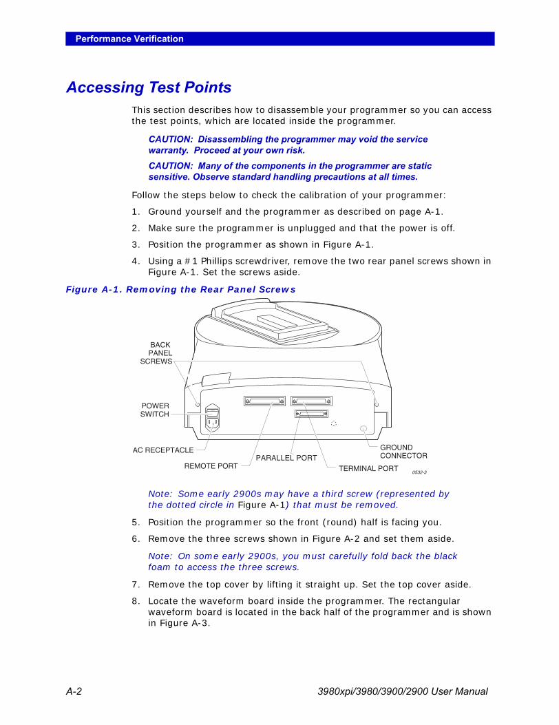
Performance Verification
A-2 3980xpi/3980/3900/2900 User Manual
Accessing Test PointsThis section describes how to disassemble your programmer so you can access the test points, which are located inside the programmer.
CAUTION: Disassembling the programmer may void the service warranty. Proceed at your own risk.CAUTION: Many of the components in the programmer are static sensitive. Observe standard handling precautions at all times.
Follow the steps below to check the calibration of your programmer:
1. Ground yourself and the programmer as described on page A-1.
2. Make sure the programmer is unplugged and that the power is off.
3. Position the programmer as shown in Figure A-1.
4. Using a #1 Phillips screwdriver, remove the two rear panel screws shown in Figure A-1. Set the screws aside.
Note: Some early 2900s may have a third screw (represented by the dotted circle in Figure A-1) that must be removed.
5. Position the programmer so the front (round) half is facing you.
6. Remove the three screws shown in Figure A-2 and set them aside.
Note: On some early 2900s, you must carefully fold back the black foam to access the three screws.
7. Remove the top cover by lifting it straight up. Set the top cover aside.
8. Locate the waveform board inside the programmer. The rectangular waveform board is located in the back half of the programmer and is shown in Figure A-3.
Figure A-1. Removing the Rear Panel Screws
0532-3
BACK PANEL
SCREWS
REMOTE PORT TERMINAL PORT
GROUNDCONNECTOR
POWERSWITCH
AC RECEPTACLEPARALLEL PORT

Performance Verification
3980xpi/3980/3900/2900 User Manual A-3
9. Locate the 78-pin connector block on the waveform board (see Figure A-3).
10.Refer to Figure A-4 for the location of the pins on the connector (pin numbers are not silk-screened on the board) and mark the following pins on the connector block using small pieces of tape:
Pin 72Pin 1 (ground)Pin 78 (+10V)Pin 24 (+15V)Pin 28 (8 MHz)
Note: Testing the wrong pins on the connector block will yield invalid calibration readings.
Figure A-2. Removing the Top Cover Screws
Figure A-3. Waveform Board
SCREWS
0727-3
1548-2
WAVEFORMBOARD
78-PINCONNECTORBLOCK

Performance Verification
A-4 3980xpi/3980/3900/2900 User Manual
Checking the Master Clock1. Plug in the programmer and turn on the power switch.
2. Check the 8 MHz clock signal by placing the ground probe of your frequency counter (or oscilloscope) on pin 1 (ground) of the 78-pin connector block. Place the test probe on pin 28 shown in Figure A-4.
WARNING: Make sure the ground and test probes are on the correct pins.The clock signal should read as follows:
Checking the Reference Voltages3. Check the +10 voltage reference by placing one probe of your digital
multimeter on pin 78 (+10V) of the 78-pin connector. Place the other probe on pin 1 (ground). Both pin locations are shown Figure A-4.
WARNING: Make sure the probes are on the correct connector pins.
Figure A-4. Test Points on the Connector Block
Minimum Nominal Maximum7.999 MHz 8.000 MHz 8.001 MHz
1577-2
PIN 24 (+15V)
PIN 72(Plugged)
PIN 78 (+10V)
1
39
78
40
PIN 1 (GROUND)
PIN 28 (8MHz)

Performance Verification
3980xpi/3980/3900/2900 User Manual A-5
The +10V signal should read as follows:
4. Check the +15 volt supply by placing one probe of your digital multimeter on pin 24 (+15V) of the 78-pin connector. Place the other probe on pin 1 (ground). Both pin locations are shown in Figure A-4.
WARNING: Make sure the probes are on the correct connector pins.
The +15V signal should read as follows:
You are now finished checking the calibration of your programmer. If the reference voltages and master clock match the listed specifications, your programmer is operating within factory specifications.
Reassembling the ProgrammerFollow the steps below to reassemble your programmer:
1. Set the top cover back onto the programmer.
2. Using a #1 Phillips screwdriver, replace the two (or three) screws you removed from the rear panel in step 4. See Figure A-1 for the location of the screw holes.
3. Using a #1 Phillips screwdriver, replace the three screws you removed from the top of the programmer in step 6. See Figure A-2 for the location of the screw holes.
Your programmer is reassembled and ready for use.
Minimum Nominal Maximum
+9.990V +10.000V +10.010V
Minimum Nominal Maximum
+14.25V +15.00V +15.75V

3980xpi/3980/3900/2900 User Manual B-1
B Computer Remote Control
The programmer can be controlled via a host computer using Computer Remote Control (CRC) protocol. CRC commands have been designed to be incorporated into a remote computer software program (driver) that will allow an operator to control the programmer. The driver generates commands and sends them to the programmer, which executes the commands. The programmer then returns a response character, and in some cases, data. The driver reacts to the response and uses it to generate messages and prompts for the user.
Note: You do not need to use CRC if you are using TaskLink or are accessing the programmer's built-in menu system (using HiTerm or a similar product to communicate with the programmer). CRC commands offer you an alternative, allowing you to create your own custom interface with the programmer.
This chapter is not intended to be a complete guide to using CRC commands. For a more detailed explanation of CRC commands, refer to the “UniSystem Computer Remote Control” Application Note (983-0490) available from Customer Support.
This chapter contains the following information:
System Setup — Explains how to set up the programmer for remote control operation. Includes information on entering and exiting CRC mode.CRC Summary — Lists the available CRC commands.
If you are using CRC commands, you must use a driver program to send the CRC commands and receive the programmer's responses. You can either write your own software driver or use an already created driver (such as the terminal.exe program included with Windows).
System SetupThe programmer receives CRC commands and sends responses to the host computer through an RS-232C port using a 25-pin D connector in two possible configurations: either DTE or DCE. Only the Remote port supports CRC operation.
The pin designations for the Remote port are shown on page 2-9. Included in that section is a table of pin definitions that describes the function of each pin for the two serial port configurations.
To ensure correct operation of the Remote port with the host computer, set the parameters for the Remote port according to the host computer requirements.

Computer Remote Control
B-2 3980xpi/3980/3900/2900 User Manual
Entering CRC ModeCRC mode can be entered automatically at powerup or by using the Remote Control menu.
Note: Before you enter CRC mode with a new version of software, you must use the Update command to update the system software. Refer to the description of the Update command in the “Commands” chapter.
By Menu CommandsTo enter CRC mode using the Remote Control menu, do the following:
1. Press F1 to go to the Main Menu.
2. Type M to select the More Commands menu.
3. Press R to select Computer Remote Control.
The programmer is now in Remote Control mode. Except for CTRL+Z, all keyboard input will be ignored.
On PowerupThe programmer enters either terminal or CRC mode during powerup based on the following combination of port connections and parameter settings.
Note: X = don't care condition
If you want the programmer to power up in CRC, perform the following steps:
1. Press F1 to get to the Main Menu.
2. Type M to select the More Commands menu.
3. Press C to select the Configure System menu.
4. Press E to select Edit from the Configure Systems menu.
5. Press I to select Interface from the Edit menu. The programmer displays the interface parameters.
Parameter Settings Port Connections
Power UpCRC
UserMenu Port
TerminalConnected
Remote Connected Result
Off T (Terminal) Yes Yes Terminal mode on Terminal port
Off T (Terminal) No Yes CRC mode on Remote port
Off R (Remote) X Yes Terminal mode on Remote port
On X X Yes CRC mode on Remote port
X X Yes No Terminal mode on Terminal port

Computer Remote Control
3980xpi/3980/3900/2900 User Manual B-3
6. Move the cursor to the Power on CRC field and press Y. CRC is now selected. The following steps in this procedure save CRC mode as a powerup system parameter.
7. Press F2 two times to return to the Configure System Parameters menu.
8. Press S to select Save from the Configure System Parameters menu. The screen displays the Save System Parameters menu.
9. Type 1 ENTER to select the Powerup Defaults file as the one where system parameters will be saved.
10. Press ENTER again so that the selection will be saved to the disk. The next time you power up the programmer, it will enter CRC mode automatically.
Interface ModesYou can operate the programmer in one of two interface modes: Terminal and CRC. In Terminal mode you use screens and menus to interact with the programmer. In CRC mode you send single-line commands to the programmer and the programmer responds with single line prompts, responses, and error codes.
Note: Terminal mode operations may be run from either the Terminal port or the Remote port. CRC mode operations must be run from the Remote port; CRC will not work on the Terminal port.
Depending on the equipment you have connected to the programmer, and on the settings of the User Menu Port and Power-on CRC parameters, you can select which mode is available on which port. (The User Menu Port parameter is found on the More Commands/Configure System/Edit/Communication Parameters screen.)
Factory defaults for the programmer are Terminal mode commands sent through the Terminal port and CRC mode commands sent through the Remote port. The factory default for power-up state is Terminal mode.
Exiting CRC ModePress CTRL+Z to exit CRC from an ASCII terminal on the Terminal port.
From a remote computer, send the Z ENTER command. If you exit remote mode using the Z ENTER command, the programmer's parameters are set to what they were before you entered remote mode. If you exit using CTRL+Z, the programmer's parameters are NOT changed.
Suspending CRC ModeCRC Mode can be suspended temporarily to allow you to go into terminal mode to view or change parameter settings or the device data in memory. If the User Menu Port is set to T (Terminal port) press CTRL+Z to suspend CRC Mode. If you are controlling the programmer from the Remote port, send the 49] command.

Computer Remote Control
B-4 3980xpi/3980/3900/2900 User Manual
Halting CRC OperationsTo halt any command or any ongoing CRC operation, use one of the following commands from the Remote port. Neither of the following two commands requires an ENTER. Both commands are immediate and both terminate any preceding command operation.
CRC Default SettingsWhen CRC mode is entered, certain defaults are set prior to the programmer's accepting any commands. The default settings are outlined below:
ASCII Command
Hex Code Description
Esc 1B Causes the programmer to unconditionally halt all operations except a binary transfer.
BREAK n/a Causes the programmer to unconditionally halt any operation in progress. This includes all data communications transfers. The data line must be held in the spacing condition for 110 ms to 700 ms.
Description Setting
Upload/download port Remote port
Data source/destination RAM
Security fuse data (0 or 1) 0
Program security fuse No
Reject option (commercial or single) Commercial
Logic verification option All
Number of verify passes (0,1 or 2) 2
Fill RAM before downloading No
Illegal bit check option No
Blank check option No
Enable yield tally option No
EE bulk erase option No
Odd/even byte swap for 16 bit option No
JEDEC I/O translate DIP/LCC option Yes
Continuity check option Yes
Compare electronic signature Yes
Host command Blank
I/O address offset 0
I/O format MOS technology (format 81)
Instrument control code (0,1, 2) 0
I/O timeout 30 seconds
Upload wait 0 seconds
Number of nulls 255

Computer Remote Control
3980xpi/3980/3900/2900 User Manual B-5
If you exit remote mode using the Z command, the programmer's parameters are set to what they were before you entered remote mode. If you exit using CTRL + Z, the programmer's parameters are NOT changed.
CRC CommandsCRC commands are simplified commands for the programmer that are designed to be received from a controlling computer. Because the commands are so simplified, they can be cryptic at times.
CRC Command SummaryYou send CRC commands to the programmer by typing the command and then pressing the ENTER key. When the programmer receives a CRC command, the command is executed and a response is sent back, followed by a carriage return. If the response is an F, an error occurred. If the response is a ?, the programmer did not understand the command. If the response is a >, the normal CRC prompt, the command executed properly. Some commands respond with both a value and the prompt. For example, the programmer might return 00284295> when you send the Calculate Sumcheck command. In this case, the 00284295 is the sumcheck and the > indicates that the command executed properly. The I, O, and C commands perform any data transfer prior to sending the response.
Each command in the CRC command set is summarized in the following tables. For a more detailed explanation of CRC commands, refer to the “UniSystem Computer Remote Control” Application Note (983-0490) available from Customer Support. The command tables are broken up into standard and extended CRC commands. Standard CRC commands are commonly used commands, such as Load, Program, and Verify. Extended CRC commands are more specific device-related commands, such as Set Security Fuse, Fill Fuse Map, and Set Vector Test Options.
Note: While in CRC mode, the programmer recognizes only uppercase characters.
Except where noted, the commands use the following notation conventions: lower-case alphabetic characters indicate arguments that must be specifiedh represents a hexadecimal digit. n represents a decimal digit. xxx...xxxx represents a string of characters. Filenames are limited to 12 total characters: name (eight characters), a period (one character), and an extension (three characters).
For example, nn02] indicates that you may precede the 02] command with two decimal digits.
Serial set auto-increment mode No
Programming mode single device
Total set size 1
Upload EOF delimiter flag Disabled
Download EOF delimiter flag Disabled
Description Setting
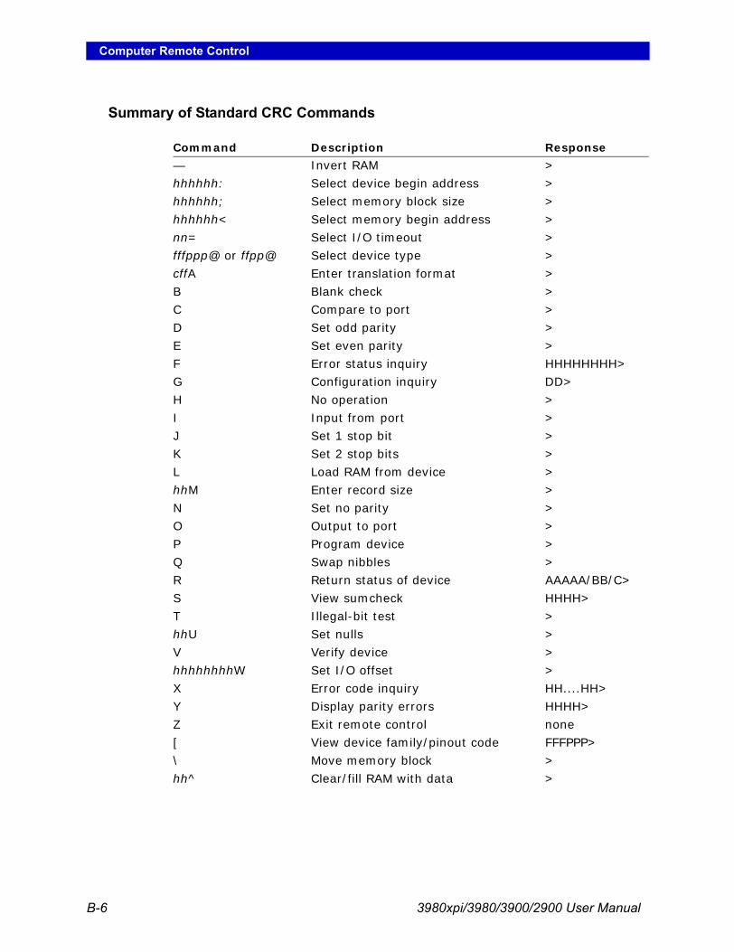
Computer Remote Control
B-6 3980xpi/3980/3900/2900 User Manual
Summary of Standard CRC Commands
Command Description Response
— Invert RAM >hhhhhh: Select device begin address >hhhhhh; Select memory block size >hhhhhh< Select memory begin address >nn= Select I/O timeout >fffppp@ or ffpp@ Select device type >cffA Enter translation format >B Blank check >C Compare to port >D Set odd parity >E Set even parity >F Error status inquiry HHHHHHHH>G Configuration inquiry DD>H No operation >I Input from port >J Set 1 stop bit >K Set 2 stop bits >L Load RAM from device >hhM Enter record size >N Set no parity >O Output to port >P Program device >Q Swap nibbles >R Return status of device AAAAA/BB/C>S View sumcheck HHHH>T Illegal-bit test >hhU Set nulls >V Verify device >hhhhhhhhW Set I/O offset >X Error code inquiry HH....HH>Y Display parity errors HHHH>Z Exit remote control none[ View device family/pinout code FFFPPP>\ Move memory block >hh^ Clear/fill RAM with data >

Computer Remote Control
3980xpi/3980/3900/2900 User Manual B-7
Summary of Extended CRC Commands
Command Description Response
01] Display system configuration SSSS/AAAA/MM/PP/II/JJ>nn02] Set upload wait time >n03] Set device ID verify option HHHHHHHH> or >nn04] Set Remote port baud rate >xxx...xxxx05] Set host command >n06] Select data bits >n07] Set next set member >xx09] Set set size >nn22] Set data word width >n23] Select number of verify passes >n24] Select security fuse programming >n26] Specify logic verify options >n27] Set/clear enable/disable sec. fuse >n28] Fill fuse map >n29] Set reject count option >hhh2A] or hh2A] Enable programming options >hhh2B] or hh2B] Disable programming options >nhh2C] Select memory fill option >hh2D] Vector test options >2F] Return 8-character sumcheck HHHHHHHH>xxx...xxxx30] Set data file name >n31] Set data source/destination >xxx...xxxx33] Select device manufacturer >xxx...xxxx34] Select device part number >xxx...xxxx38] Load file from disk >xxx...xxxx3B] Delete disk file >n3C] Set data transfer port >xxx...xxxx3E] Select Keep Current algorithm > 39] Delete all RAM files >n40] Upload device information See Application Noten41] Perform self-tests and upload results AAA...AA>43] Upload yield tally See Application Note46] Clear yield tally >49] Suspend CRC mode Displays terminal screenn4A] Get filename from disk AAA...AA>n4D] Select algorithm type (0,1,2,3) >n4F] Set RAM device selection >n52] Select algorithm source for floppy disk
(MSM not available)>

Computer Remote Control
B-8 3980xpi/3980/3900/2900 User Manual
xxx...xxxx53] Save RAM data to disk file >54] Upload device footnote See Application Note55] Upload device-specific message See Application Note56] Upload memory verify failure ddPAAAAAAAAHHhh57] Get checksum of operation See Application Note58] Upload system ID HHHH HHHH HHHH>5A] Display list of parameters See Application Note5B] Clear vector data >5C] Load system files for Custom Menu
(CM) algorithm disk>
5D] Write system files to CM disk >5E] Write algorithms to CM disk >60] Get number of sectors dd>n 61] Get sector configuration settings HHHH HHHH>nhhhhhhhh62] Get sector configuration settings >63] Reboot the programmer >xxx...xxxx64] Select device part number for CM
(use xxx.xxxx33] to select the manufacturer)
A65] Returns software version number n.nnx, where x may be a blankA7] Swap bytes >DC] Device check See Application NoteEB] Input JEDEC data from host >EC] Output JEDEC data to host >FC] Restore CRC entry default parameters >FD] Restore user-defined CRC parameters >FE] Save user-defined CRC parameters >
Command Description Response

3980xpi/3980/3900/2900 User Manual C-1
C Keep Current Subscription
The Keep Current™ subscription service keeps your programmer up-to-date with the latest features and device support. You gain immediate access to new and improved programming algorithms via the Keep Current Library accessible through the Internet or via the Data I/O BBS.
Semiconductor companies constantly introduce new devices and issue specification changes for existing devices. Incorporating these changes swiftly into your programming system ensures that you obtain the highest programming yields and best device reliability possible. Periodic update kits incorporate all changes since the previous update.
The Keep Current device support files are located on the Data I/O Bulletin Board System, on the Data I/O Web page, and through anonymous FTP.
Computer RequirementsTo access and download the Keep Current files, you need the following:
Ability to create 3.5-inch DOS disks: 720KB if you are using a UniSite, 1.44MB for all other programmers.The ability to connect to the Keep Current Library through the Internet or a modem capable of handling 2400 or greater.

Keep Current Subscription
C-2 3980xpi/3980/3900/2900 User Manual
Procedure Overview
1. Gather InformationKnowing the following information about the devices you will be programming will enable you to find the correct algorithm once you are connected.
Manufacturer (example: AMD)Device name (example: 27c1024)Package type (example: 48-pin PLCC)Current version of the programmer software (example: 5.5)
1. Gather Device Information
2. Connect to Keep Current
3. Find Device Algorithm
4. Download Algorithm
5. Use Algorithm
BBS WebPage
Does thealgorithm appearon the standard
device list?No Yes
Select Device /(1) Keep Current
More Commands /Configure System /
Keep Current /Replace-Restore
WWeb Page

Keep Current Subscription
3980xpi/3980/3900/2900 User Manual C-3
2. Connect to Keep CurrentUsing the Web
Go to the Data I/O Web Site at www.dataio.com. Click on the Keep Current image from the Home Page or from the Programmer Device Support page.
3. Find Device AlgorithmWhen you reach the Keep Current Library, select the correct algorithm. Algorithms are arranged by programmer and system software version. Keep Current filenames are represented as follows:
Each Keep Current algorithm is designed to work with a particular version of system software. Only algorithms that are compatible with the installed version of system software are displayed on the programmer’s Keep Current Part List screen.A Keep Current algorithm and a version of your programmer’s system software are compatible when the numbers to the left and immediate right of the decimal point match, as shown in the following example:
Note: Keep Current algorithms are valid for only one major release of software because they will be included with the next release of system software.
Algorithm Version
System Software Version Compatible?
3.51 3.5 Yes3.7 3.7 Yes3.6 3.7 No
xVVddddd.exe
Programmer Typeu = UniSiter = 2900s = 3900a = AutoSite/PM2500
Version Number with which this algorithm works.Data I/O Device Support Number

Keep Current Subscription
C-4 3980xpi/3980/3900/2900 User Manual
4. Download AlgorithmAlgorithms come in a self-extracting file format. Place the Keep Current file on a floppy disk that has been formatted on your programmer, and then expand the file by running it. The following files should be created:
Label the disk Keep Current and specify the version number to avoid mismatched software version numbers if you use the disk again.You can also create these files in a sub-directory and transfer the files to a disk using your programmer in terminal mode. Use the More Commands/Transfer/Download screen, select format 16 (Absolute Binary), and select Disk as the destination.
5. Use AlgorithmBefore you use a Keep Current algorithm, determine whether or not it appears on the programmer’s standard device list and follow the appropriate directions:
On Standard List—If the algorithm is listed in the standard device list, in terminal mode use More Commands/Configure System/Keep Current/Replace-Restore to add the Keep Current algorithm to the device list, ensuring that the latest algorithm is available to all programmer users. Use this algorithm as you do a regular algorithm. Refer to your programmer User Manual for instructions.Not on Standard List—If the algorithm is not listed in the standard device list, in terminal mode use Select Device / (1) Keep Current. The algorithm can be selected from the Select Device menu, but it cannot be added to the device list. Use this algorithm as you do a regular algorithm. Refer to your programmer User Manual for instructions.
Sample Keep Current ScenarioThe following example illustrates a typical Keep Current scenario:1. In May, you update your system software to version X.4. At the same time,
you enroll in the Keep Current Subscription Service.2. In June, Cruft Technologies announces a new device, the Cruft 1263.3. A week later, Data I/O announces support for the Cruft 1263 and places a
Keep Current algorithm for the Cruft 1263 on the Keep Current BBS and the Data I/O Web page.
4. The next day you connect to the Keep Current Library via the BBS or the Web page and download the new algorithm for the Cruft 1263.
5. In August, Data I/O releases version X.5 system software, complete with the new algorithm for the Cruft 1263.
6. You update your programmer to version X.5 system software. The algorithm for the Cruft 1263 is part of the system software.
File Name Description of File
xVVddddd.KCx AlgorithmxVVddddd.txt Instructions on useadapters. sys* System adaptersdevfnote.sys* Device notes * Optional file

3980xpi/3980/3900/2900 User Manual D-1
D Glossary
Action Symbol Found in the upper left corner of the screen, the action symbol rotates to indicate that the programmer is performing an operation.
Address A coded instruction designating the location of data or program segments in storage.
Address Offset A value subtracted from addresses during input translation, then added to addresses during output translation.
Algorithm The software file containing information (a sequence of voltage or current waveforms) to program a specific device.
All Parameters The All Parameters screen displays all applicable parameters on a parameter entry screen.
Approval Indication that a device manufacturer has tested an algorithm to support a specific device on a programmer. The level of an approval varies by device manufacturer, but an approval usually indicates both yield and waveform analysis.
AutoBaud A special feature on the programmer that senses the baud rate of equipment connected to the programmer and sets the programmer's baud rate to match the equipment's baud rate. AutoBaud is designed for equipment that cannot support baud rates as high as 9600 baud, such as 1200/2400 baud modems.
Base The interface between the programmer and the device. The Base routes the signals between the device and the Universal Pin Drivers inside the programmer.
Baud Rate A measure of data flow. The number of signal elements per second based on the duration of the shortest element. When each element carries one bit, the baud rate is numerically equal to bits per second.

Glossary
D-2 3980xpi/3980/3900/2900 User Manual
BGAAn acronym for Ball Grid Array, a type of device package. Usually a square device with one side populated with small solder balls as leads.
Blank Check A device check that checks a device for programmed bits. If no programmed bits are found, the device is considered blank.
Block Size The hexadecimal number of bytes to be transferred in a data transfer. The beginning of the block is defined by a begin address. The end of the block is the sum of the block size and the begin address minus one.
Byte Swap See Odd/Even Byte Swap.
Command Window The left side of the screen. At the top of the window is the menu name, displayed in uppercase letters. Below the menu name, the available commands are displayed in upper- and lowercase characters.
Communications Parameters The various settings that determine the I/O characteristics of your equipment, such as baud rate, stop bits, data bits, and handshaking.
Compare Electronic ID A command that compares the electronic signature of the socketed device against the electronic signature specified in the currently selected algorithm.
Compensated Vector Test A device test that enables load compensation on PLD output pins under test during vector testing. This may eliminate structured test errors when testing PLDs sensitive to output loading, where many of the devices register transitions simultaneously.
Computer Remote Control (CRC)A command set that may be used to operate a programmer remotely. These commands are usually the basis for external programmer drivers, which may operate a programmer from a PC or other host. See also Remote Mode.
Context-sensitive HelpInformation that changes depending on the screen position. With the programmer, every time you move the cursor to a different field, the information on the online help screen changes.
Continuity Check A device check that tests for open device pins before performing a device operation.
CRC An acronym for Computer Remote Control. See also Remote Mode.

Glossary
3980xpi/3980/3900/2900 User Manual D-3
Cross Programming A programming operation that allows a single generic programmable logic device (PLD) to be configured as any one of many PLD architectures. Consequently, the generic device can take on the function of many subset devices. For example, a 16V8 generic PLD can be configured as a 16R4, 16R8, or 16L8.
Data Bits A communication parameter that specifies the number of bits per byte.
Data Representation The manner in which the data in user memory appear on the screen. You can select either X and -, or 0 and 1, where X and 0 represent an unprogrammed state, and - and 1 represent a programmed state.
Data Translation FormatsSee Translation Formats.
Data Word Width The word width of the data to be used during a device operation. For 8-bit (or above) devices, the maximum is 64, and the minimum word width is equal to the device width. For 4-bit devices, the word width can be 4, 8, 16, or 32. This value should match the word width of the data bus in the target system for the device being programmed.
Destination The place where you are sending something, usually data. The place can be RAM, a disk file, or one of the programmer's serial ports.
Device Begin Address The first hexadecimal address of device data to use for a device operation. If programming, it represents the first address to program. If verifying, it represents the first address to verify.
Device Block Size The size of device data to be used in device operations.
Device Operation Usually a term that refers to loading, programming, or verifying. It can also refer to other available commands, such as Device Check and Electronic Erase.
Device Word Width The number of bits in the data word of the device.
DIP An acronym for Dual In-line Package, a type of device package.
Dialog Window The largest window on the screen. The dialog window displays different information and system parameters, depending on the selected command.

Glossary
D-4 3980xpi/3980/3900/2900 User Manual
Download Data A file operation that moves a data file from a host computer to the programmer's RAM or disk.
Download Echoing Displays the data being downloaded.
Download Host Command A command that is sent from the programmer to the host during a download. The command tells the host to begin sending data to the programmer.
DUARTAn acronym for Dual Universal Asynchronous Receiver/Transmitter.
E-MICRO An acronym for Programmable Microcontroller, a type of device technology.
EPROM An acronym for Erasable Programmable Read-Only Memory. (Usually refers to UV erasable memories.)
EEPROM An acronym for Electronically Erasable Programmable Read-Only Memory. The device can be either completely or partially electrically erased in circuit or on the programmer.
Electronic ID The combination of bytes that identify the device number and manufacturer of a programmable device.
Enhanced Security Fuse Capability Found on EMICROs, the Enhanced Security Fuse Capability allows security fuse data to be stored in a data file. For more information, or to see if a device supports this capability, see the device manufacturer's data book.
ESD An acronym for Electrostatic Discharge.
False Positive In programming, a misprogrammed fuse that retains minimal operational characteristics so that it passes the fuse test. These may be inadequately programmed, or over-programmed so that they will fail later in circuit.
File Transfer Operations An operation involving the transfer of data between the programmer and a host. Upload and download are file transfer operations.

Glossary
3980xpi/3980/3900/2900 User Manual D-5
Filename The name of the file to use during file operations. The filename must follow standard DOS conventions: up to eight alphanumeric characters, followed by an optional three-character file extension, with the two fields separated by a period. An example of a valid filename would be 27256.dat or filename.c.
Fuse Verification A type of post-programming device check that checks the fuse pattern programmed into a logic device with the pattern in user memory.
Fusemap The fuse-level description portion of a programmable integrated circuit. Fusemaps are typically files in JEDEC Standard #3A and are downloaded to PLD programmers for device implementation.
Handshaking The required sequence of signals for communication between two units. The I/O bus protocol for a unit defines its handshaking requirements. This is especially true for asynchronous I/O systems in which each signal requires a response to complete an I/O operation.
High-speed Download A special feature of the programmer that allows the programmer to download data from a PC at 115.2K baud.
High-speed Logic Drivers A device test that increases the speed of the logic transitions between 0 and 1, and 1 and 0 of the test vector input states. This test is a diagnostic tool designed to help debug and classify test vector failures. Specifically, this test is designed to help identify vector transitions that are speed dependent.
Host A micro, mini, or mainframe computer used to control the programmer in Remote mode. You must use a software driver, such as Data I/O's TaskLink, to allow the computer to communicate with the programmer.
Host Command (download & upload) The command that is sent from the programmer to the host system during uploading/downloading. See Download Host Command and Upload Host Command.
I/O Address Offset This value influences the beginning address where data is stored during a file transfer operation. For uploads, the I/O Offset represents the address to start loading a formatted data file. For downloads, the I/O Offset is subtracted from the beginning address in the formatted data file. The result is then added to the memory begin address to determine where the block of data is loaded.
I/O Timeout The amount of time that the programmer will wait for a data transfer to begin.

Glossary
D-6 3980xpi/3980/3900/2900 User Manual
I/O Translation Format See Translation Formats.
Illegal Bit An illegal bit occurs when a device contains a programmed location and the data file specifies that the location should be unprogrammed.
Illegal Bit Check A test that determines whether or not a socketed device contains any illegal bits.
Instrument Control Code A 1-digit number that signals or controls data transfers. It also implements a form of remote control that provides peripherals with flow control beyond that provided by software handshaking.
JEDEC Joint Electron Design Engineering Committee: a committee of programmer and semiconductor manufacturers that provides common standards for programmable issues. Examples include acceptable test characters for PLDs and standard data transfer/programming formats for PLDs.
JEDEC Standard #3A The standard PLD data translation format, as defined by JEDEC for PLD design software to communicate with PLD programmers. It defines the states of all fuses in the device (the fusemap) and may include test vectors for DEVICE testing.
JEDEC I/O Translate DIP/LCC Vectors A feature on the programmer that translates test vectors for a device from its DIP package to its PLCC/LCC package, allowing for the different pinouts of the two package types.
JLCCAn acronym for J-style Leadless Chip (or Ceramic) Carrier, a type of device package. A device with hooked leads that are open at one end (leads are usually on all four sides).
Job File A sequence of keystrokes that have been stored in a disk file and which can be played back at a later time.
Keep Current Subscription ServiceA one-year renewable subscription that provides periodic update kits containing the latest features and device support for Data I/O products.
LCA An acronym for Logic Cell Array, a reconfigurable programmer gate array manufactured by Xilinx Corporation.

Glossary
3980xpi/3980/3900/2900 User Manual D-7
LCC An acronym for Leadless Chip Carrier, a type of device package. A 4-sided ceramic package with pads on the underside for surface mount applications.
LED An acronym for Light Emitting Diode. The programmer has five LEDs: four on the top cover and one on the disk drive.
Load Data A device operation that moves device data into the programmer. You can load the programmer with data from a device, from the programmer's internal disk drive, or from a serial port (for example, from the Remote port).
Load Device A device operation that copies data from a master device into User memory.
Logic Verification After programming a device, you can select test vector verification, fuse verification, or both types of verification.
Master Device A device that contains data you wish to program into another device. For example, you would load data from a master device and then program that data into a blank device.
Mass Storage Module (MSM)The MSM optimizes programmer performance by providing storage for system software and programming algorithms, which enables fast boot-up and eliminates the need to access files from the 3-1/2” disk drive.
MatchBook A durable plastic carrier that handles surface-mount devices, such as LCCs, PLCCs, SOICs, and PGAs during programming.
Memory Begin Address The first address, in hex, of the first byte of data to be used in device operations. If the data source/destination is RAM, the memory begin address is a RAM address. If the data source/destination is disk, the memory begin address is the offset for a disk file.
Message Bar The fourth line of the screen. The programmer displays system and error messages in the message bar. The action symbol is also located in the message bar.
MicroBGAAlso µBGA or mBGA, short for Micro Ball Grid Array. A small, thin device package with area array-compliant bumps. Trademarked by Tessera, Inc.

Glossary
D-8 3980xpi/3980/3900/2900 User Manual
Next Device Used during serial set programming, this value specifies the next device in the set. For example, if you are using 8-bit devices and have specified a word width of 16 bits, it will require two devices to store each 16-bit word. Depending on the value entered, the data programmed into the next device will come from either even addresses or odd addresses.
Non-default Parameters The Non-default parameters screen displays a selected group of parameters on a parameter entry screen. To display all the available parameters, press F4 to toggle to the All Parameters screen.
Odd/Even Byte Swap Used during device operations for 16-bit devices, this option swaps the Most Significant Bytes (MSB) and the Least Significant Bytes (LSB) of 16-bit words. The programmer stores RAM data and disk file data with the convention that the LSB of a 16-bit word resides in the even byte of memory.
Online Help Available throughout the programmer, the help screens provide you with both general help and context-sensitive help. The Help screen is divided into four sections: the key listing, the general help, the specific help, and the reminder bar.
Output Record Size The number of data bytes contained in each data record during upload.
Overblow A condition in which fuses are blown that should not have been.
Overblown Fuse A fuse that has been over-programmed such that the surrounding area may have been damaged or such that fuse material splatter was created. Splatter (or rattlers) can cause intermittent shorting.
PAL®
An acronym for Programmable Array Logic. PALs are devices with programmable AND and fixed OR arrays. This is a slightly different architecture from a PROM or an FPLA. Other examples of PAL-type architectures from other manufacturers include PEEL and GAL. A registered trademark of Advanced Micro Devices, Inc.
Parallel Test Vector Application Use of internal registers to hold and release a full set of test vectors (e.g., 20 for a 10-input 10-output device) at once. In contrast to serial application, parallel does not require accommodations for clocking contention, and parallel better matches in-circuit PLD operation and board test suites.
Part Number The number on the device. For example if you are using an Intel 27C256, the part number of the device is 27C256.

Glossary
3980xpi/3980/3900/2900 User Manual D-9
Pin Driver The electric circuit reading or applying voltage and current pulses to the individual pin of a device, for programming or testing. See also Universal Pin Driver.
PGAAn acronym for Pin Grid Array, a type of device package. Usually a square device with one side populated with small pins as leads.
PLCC An acronym for Plastic Leaded Chip Carrier, a device package with J-shaped leads extending from four sides downward, used for surface mount applications.
PLD An acronym for Programmable Logic Device, a type of programmable integrated circuit. Architectures range from very simple to very complex. Most PLDs contain two levels of logic, an AND array followed by an OR array.
PROM An acronym for Programmable Read-Only Memory. A device with fixed AND and programmable OR arrays. This is a slightly different architecture from an FPLA or a PAL.
Program The controlled application of electrical pulses to program specific fuses or cells.
Program Device A device operation that copies device data into a socketed device. The programming is done according to the programming algorithm selected in the select device stage. The programming operation can also include a verify operation.
Program Security Fuse A programming parameter that enables/disables the programming of the device's security fuse.
Program Signature Available on only a few devices, the Program Signature is a user-definable field that allows the user to program data into the program signature array. For example, the Program Signature could contain the revision level or modification date of the data in the remainder of the device.
Programmable Integrated Circuit One of the four basic categories of ASICs: the other three being gate arrays, standard cells, and full custom devices. PICs are ICs that are user configurable. PLDs and PGAs are examples of programmable integrated circuits.

Glossary
D-10 3980xpi/3980/3900/2900 User Manual
QFPAn acronym for Quad Flat Pack, a type of device package. A square or rectangular device with leads on all four edges (leads can be either straight or gull-wing). BQFP (Bumper Quad Flat Pack) is a QFP with bumpers on the corners to prevent damage to leads. CQFP is a Ceramic QFP or a QFP with carrier. Long Lead Carrier QFP is an ACTEL product with long leads attached to a carrier grid for handling ease. PQFP (Plastic carrier QFP) is a QFP with a plastic protective carrier for handling ease. QFPCAR is a QFP in a carrier. TQFP is a thin QFP.
QUIPAn acronym for Quad Inline Package, a type of device package. Similar to DIP, but with staggered long & short leads (leads on long sides).
Reboot The process of re-initializing the programmer. After rebooting, the programmer is in the same state as if it had just been turned on.
Registered Devices Devices that contain registers, rather than being combinatorial only. Registered devices are typically used for sequencers and state machine designs. Typical examples are 16R8, 82S159, and 22V10.
Reject Option A post-programming device check that pulses the programmed device with voltage to see if the device has programmed per specification. The number of times a device is pulsed varies by manufacturer and by the reject option you select.
Reminder Bar The bottom line of the screen. The reminder bar tells you what function keys are available and what they will do if pressed.
Remote Mode The programmer is controlled from a host running a driver program. Device data files can be stored on the programmer's disk and on the host.
SDIPAn acronym for Shrink Dual Inline Package. An SDIP device is the same as DIP but has more leads at higher pitch.
Security Fuse A location in a programmable device that, when programmed, secures the device from readback: the data in the device is unreadable.
Security Fuse Data The actual data to program into the device's security fuse.
Select Device A procedure that tells the programmer what device you will be using. You select a device by selecting the manufacturer and the device part number.

Glossary
3980xpi/3980/3900/2900 User Manual D-11
Self-test A built-in self-diagnosis command that allows you to test various circuits and subsystems in the programmer, verifying proper operation or isolating possible problem areas.
Serial Set A method of set programming in which the devices of the set are programmed one at a time instead of all at once.
Serial Test Vector Application The process of applying test vectors in a serial fashion, one input at a time.
Serial Vector Test A device test that applies test vector input states serially, starting with pin one and stepping through the remaining pins. This test is a diagnostic tool designed to help debug and classify test vector failures. Specifically, this test is designed to isolate test vectors that are sequence dependent.
Set Programming A type of programming in which a large data file is partitioned and programmed into multiple memory devices.
SIMMAn Acronym for Single Inline Memory Module, a type of device package. A rectangular device with leads on one long edge.
SmartPort A feature of the programmer that automatically detects and adjusts the programmer to the presence of DCE/DTE protocol.
SOICAn acronym for Small Outline Integrated Circuit, a type of device package. A rectangular device with gull-wing leads on the long sides. SOP is Small Outline Package. SO is Small Outline.
Source The place from which something is being sent, usually data. It can be sent to RAM, a disk file, or one of the programmer's serial ports.
SSOPAn acronym for Shrink Small Outline Package, a type of device package. An SOP with more leads at higher and finer pitch. Also called TSOP II.
Status Window The top three lines of the screen. The following information is displayed in the status window: the name of the data file, the amount of user RAM, the version numbers of the algorithm/system disk, the device manufacturer and part number, the family/pinout code, and the data translation format.

Glossary
D-12 3980xpi/3980/3900/2900 User Manual
Structured Test Vectors A string of test conditions applied to a PLD in a programmer/tester to stimulate inputs and test outputs to ensure functionality. A test vector is one such string: for instance, 20 characters for a 20-pin PLD, with 10 input signals and 10 expected outputs.
Structured Test Vectors (design) Structured vectors created by the design engineer to confirm that the design is operating as intended: for instance, that a 10-bit counter is counting to 10. Design vectors are used both in preprogramming simulation and in manufacturing.
Structured Test Vectors (device) Structured vectors created by the design engineer, test engineer, or an automatic test vector generation program, which confirm that the device is operating properly after programming. For instance, structured vectors can ensure that nothing can happen in the device to prevent the 10-bit counter from operating correctly. An exhaustive set of device vectors will assure that no undetectable faults may occur.
Sumcheck A 4- or 8-digit hexadecimal number that, when compared to the original data, allows you to verify that a copy of the data matches the original data. Memory devices have 8-digit sumchecks and logic devices have 4-digit sumchecks. For devices in a set, you can calculate the individual sumcheck of the device and the sumcheck of the entire set.
Terminal Emulator A program to enable a PC or other computer to act as an ASCII terminal. Allows a PC to be used to communicate with a programmer in terminal mode or with a mainframe.
Terminal Mode One of the programmer's three operating modes. The programmer is controlled from either a dedicated terminal or a workstation running a terminal emulation package. Device data files can be stored on the programmer's disk (and on the workstation).
Test Vector Test vectors functionally test the device, using structured test vectors stored in memory or in a disk file.
Test Vector Stretching Conversion of DIP test vectors to equivalent PLCC test vectors by adding don't care vector characters into the string to correspond with the PLCC's dead pins.
Total set size Used during serial set programming, this value specifies how many devices are in a set.
Translate DIP/LCC Vectors See JEDEC I/O Translate DIP/LCC Vectors.

Glossary
3980xpi/3980/3900/2900 User Manual D-13
Translation Formats A form of transmission protocol, these formats are used when transferring data between the programmer and a host computer. The different formats represent different ways of encoding the device data in a data file. The data file could contain the fuse pattern for a logic device or the data for a memory device.
Transmit Pacing The number of milliseconds the programmer will insert as a time-delay between characters transmitted to the host computer during uploading. The time delay is specified in tenths of milliseconds.
Transparent Mode One of the programmer's three operating modes. The programmer is controlled from either a dedicated terminal or from a workstation running a terminal emulation package.
TSOPAn acronym for Thin Small Outline Package, a type of device package. A rectangular device with gull-wing leads on the short sides. Also called TSOP I.
Underblow A condition in which fuses that should have been blown or programmed were not.
Underblown Fuse A fuse that did not disconnect as per manufacturer's specifications. These fuses may test properly but tend to be more prone to grow back when in circuit, rendering the PLD useless.
Universal Pin Driver A pin driver with the ability to supply power and ground to every pin. With Universal Pin Drivers, you can program and test devices without having to use pin out adapters and characterizers.
Universal PLD Programmer A programmer that can apply power, ground, and any programming pulse required to program any fuse technology device.
Upload Data A file transfer operation that involves sending data from the programmer to a host.
Upload Host Command A command that is sent from the programmer to the host during an upload. The command tells the host what to do with the incoming data.
Upload Wait The length of time the programmer will wait before it begins sending data to the host computer after the host upload command is sent.

Glossary
D-14 3980xpi/3980/3900/2900 User Manual
User Data Size The hexadecimal number of bytes of a data block to use for a device operation. Normally, this value is equal to the device size. During serial set operations, this value works with Total Set Size to determine the total amount of bytes to program into a set of devices.
User Memory The workspace used during device operations. It can be either internal RAM or a disk file. Normally, RAM is used for small, quick device operations, such as programming a single device, while disk is used for larger device operations, such as serial set programming.
User Menu Data The information you see when you look at the programmer screen. It includes such items as the dialog window, reminder bar, and message bar.
User Menu Port The port to which the user menu data is sent. You can re-direct user menu data to either the Terminal port or the Remote port.
User RAM The RAM in the programmer. User RAM can be used as a source/destination for an operation. Several operations use User RAM as a temporary storage buffer, overwriting any data that may have been there previously.
Verify Device A device operation that compares data in a programmed device with data in RAM or in a disk file. With logic devices, verifying can also include functional testing. Verify is an automatic part of the program operation, but additional verify operations can provide useful information about any errors.
Verify Pass A verify pass is a trip through a device at a specified Vcc to see if the device programmed properly. The pass is usually done once at 5V. The pass can also be done twice, with the first pass at 5.5V and the second pass at 4.5V.
Waveforms Images of the programming pulses that program a device. Waveforms are usually created by programmer manufacturers and submitted to device manufacturers as part of the approval process and to record the correct programming spec for a specific device.
Wildcard Used when entering filenames, a wild card represents one or more characters in a filename. For example, 27*.dat represents both 27512.dat and 27128.dat.

Glossary
3980xpi/3980/3900/2900 User Manual D-15
Workstation A PC or other micro computer used for local control of the programmer. You must use terminal emulation software, such as Data I/O's HiTerm, to allow the programmer and the PC (or other micro) to communicate. The programmer is designed to be compatible with all popular design workstations, including both DOS and UNIX-based workstations.
Yield The percentage of successfully programmed devices.
Yield Tally The yield tally function keeps track of the programming statistics for the last 16 types of devices programmed. The following statistics are kept for each device type: the manufacturer name and part number, the family/pinout code, the number of devices attempted, the number of devices that programmed successfully, the number of devices that failed non-blank test or illegal bit check, the number of devices that failed to verify, the number of devices that could not be programmed because they contained bits that required more programming pulses than were specified, and, for logic devices only, the number of devices that failed structured vector test.
ZIF Socket An acronym for Zero Insertion Force. A socket in which the device can be dropped in and engaged via a lever.

Index
3980xpi/3980/3900/2900 User Manual Index-1
AAbort on Empty Socket
default setting, 4-3Edit Programming Parameters, 4-25
ac receptacle, 1-4Accessory package, 1-8Algorithm Source
default setting, 4-3Edit Programming Parameters, 4-21
Algorithm typeProgramming Parameters, 4-21selecting, 4-5
Algorithm/System Disk, 1-4duplicating, 1-4inserting, 2-11
Antistatic wrist strapconnecting to, 2-15minimum resistance, 2-15, A-1
AutoBaud, 2-17running, 2-17, 3-12User Menu Port, 2-17
BBack panel, 1-4Base, 1-8
conductive pad, 2-32installing, 2-12MatchBooks, 1-8PPI, 2-27
Baud rates, editing serial port configuration, 4-25
Blank Checkdefault setting, 4-3Edit Programming Parameters, 4-23overview, 4-42Program Logic Device, 4-11Program Memory Device, 4-14
Blank Device Checks, 4-42Block Size
Complement Data, 4-51Fill Memory, 4-52Move Data, 4-52Swap Data, 4-53
Boot disk, 1-5
Booting the programmer, 2-15, 2-35, 3-12Bulletin Board Service, 1-8
CCables
building your own, 2-9electromagnetic interference, 2-4, 2-5,
2-7shielding, 2-4, 2-5, 2-7
Calculate Sumcheck, 4-39logic device, 4-39
Calibrationverifying performance, A-1
Cancelling an operation, 3-12Certificate of Compliance, 1-7Checksum Calculation
Edit Programming Parameters, 4-22Clear Vectors, 4-48Command window, 3-10Commands, running, 3-12Communication parameters, changing, 4-26Compare Data, 4-64Compare Electronic ID, 4-41
default setting, 4-3Edit Programming Parameters, 4-23Load Memory Device, 4-10Program Memory Device, 4-14Verify Memory Device, 4-17
Compatible terminals list, 4-31Compensated Vector Test
Edit Programming Parameters, 4-25Complement Data, 4-51Computer remote control
command summary, 7-5default settings, 7-4entering, 4-59entering CRC Mode, 7-2exiting, 4-59, 7-3halting an operation, 7-4powerup CRC mode, 7-2system setup, 7-1
Conductive pad care, 2-32Configuration, choosing, 2-1Configure System, 4-19Configuring
Index

Index
Index-2 3980xpi/3980/3900/2900 User Manual
devices, 4-44peripherals, 2-6, 2-7
Connecting to a PC, 2-2Connections, checking, 2-17Contents of package, 1-2Continuity Check
default setting, 4-3Edit Programming Parameters, 4-24
Copy Data File, 4-56Cross programming overview, 4-6Cursor control, 3-11Custom Menu algorithms, 4-34
Add, 4-36Create, 4-35Delete, 4-37updating, 4-38View, 4-37
DData
editing, 3-31loading from a device, 3-20, 4-8loading from a host, 3-28loading from a PC, 3-26loading from disk, 3-23
Data BitsEdit Serial Port Configuration, 4-26
Data destinationdefault setting, 4-3
Data File Directory, 4-53Data Location
Compare Data, 4-64Data Representation
Edit Fuse Map, 4-45Data source
default setting, 4-3Data translation format
default setting, 4-3selecting, 4-65
Data Word Widthdefault setting, 4-3Edit Programming Parameters, 4-22Illegal Bit Check Memory Device, 4-42Load Memory Device, 4-8Program Memory Device, 4-12Sumcheck Memory Device, 4-40Verify Memory Device, 4-16
Default (factory) settings, 4-3Delete File
Keep Current, 4-33Destination
Download Data, 4-61Edit Communication Parameters, 4-26Input from Disk, 4-66Output Logic Data, 4-68Output Memory Data, 4-68Upload Data, 4-63
Device Begin Addressdefault setting, 4-3Edit Programming Parameters, 4-23Load Memory Device, 4-9Program Memory Device, 4-13Verify Memory Device, 4-17
Device Block Sizedefault setting, 4-3Edit Programming Parameters, 4-23Load Memory Device, 4-9Program Memory Device, 4-13Verify Memory Device, 4-17
Device Checks, 4-39Device Configure Command, 4-44Device insertion error when using
elastomeric pad (error message), 6-11
Device List Disk, 1-2Device overcurrent fault (error message), 6-
13Device programming error (error message),
6-14Device support, 1-2Devices
configuring, 4-44inserting DIP, 2-22inserting PLCC or LCC into a MatchBook,
2-24inserting QFP, 2-30inserting SDIP, 2-31inserting SOIC, 2-31inserting TSOP, 2-29programming, 3-33selecting, 4-5verifying, 3-35
Dialog window, 3-11Disks
PC, 1-5programmer, 1-4write protection, 2-11
Display Device Footnotedefault setting, 4-3Edit Programming Parameters, 4-25

Index
3980xpi/3980/3900/2900 User Manual Index-3
DOS, Duplicate Disk command, 4-56Download
Keep Current algorithm, 8-4Download Data, 4-61Download Echoing
Edit Communication Parameters, 4-27Download End-of-file Delimiter
Edit Communication Parameters, 4-29Download Host Command
Compare Data, 4-65default setting, 4-3, 4-62Download Data, 4-62Edit Communication Parameters, 4-29
Downloading data from a host (session), 3-28
Downloading data from a PC (session), 3-26Duplicate Disk, 4-56
after first use, 1-4
EEdit Address Offset
Edit Memory, 4-49Edit Begin Address
Edit Memory, 4-49Edit Begin Vector
Edit Test Vectors, 4-46Edit Communication Parameters, 4-29Edit Data, 4-45
logic device, 4-45memory devices, 4-49
Edit Data Word WidthEdit Memory Data, 4-49
Edit Fuse Map, 4-45restoring data, 4-46
Edit Memory DataEditor Commands, 4-50
Edit Programmer Memory, 4-49Edit Vector
commands, 4-47overview, 4-46restoring edits, 4-48saving edits, 4-48
Editing data (session), 3-31EE Bulk Erase, 4-42
default setting, 4-3Electrical shock, avoiding, 2-15Electromagnetic Interference (EMI), 1-7
minimizing, 2-4, 2-5, 2-7
Electronic ID verify error on memory device (error message), 6-16
Electronically Erase Device, 4-42Electrostatic discharge (ESD), 1-6, 2-15, A-
1Enable CTS/DTR
Edit Serial Port Configuration, 4-26Enable Terminal Beeps
Edit Interface Parameters, 4-30Enable Yield Tally
Edit Programming Parameters, 4-23Program Logic Device, 4-11Program Memory Device, 4-14
Enhanced security fuse capability, 4-14Erase EE Device
device configure, 4-44Edit Programming Parameters, 4-23Program Memory Device, 4-14
ESD precautions, A-1Extended algorithm, selecting, 4-7Extended CRC Commands, list, 7-7External features, 1-3
FFactory default settings, 4-3Features
back panel, 1-4front panel, 1-3
File Menu, 3-23File Operations, 4-53Filename
Compare Data, 4-64default setting, 4-3Download Data, 4-61Edit Fuse Map, 4-45Edit Memory, 4-49Edit Test Vectors, 4-46Input from Disk, 4-66Load File, 4-54Output Logic Data, 4-68Output Memory Data, 4-68Output to Disk, 4-67Save File, 4-55Sumcheck Logic Device, 4-39Upload Data, 4-63Verify Logic Device, 4-15wildcards, 4-56
Fill DataEdit Communication Parameters, 4-28

Index
Index-4 3980xpi/3980/3900/2900 User Manual
Fill Memory, 4-52Edit Communication Parameters, 4-27
Fill Programmer Fuse Map, 4-48Fill Programmer Memory, 4-52Fill Variable
Fill Memory, 4-52For Member X of Y
Sumcheck Memory Device, 4-40Format Disk, 4-57Format list, 5-1From Memory Address
Move Data, 4-52Front panel features, 1-3Functional specifications, 1-6, 1-7
GGeneric PLD and cross programming, 4-6Ground connector, 1-4, 2-15
HHalting an operation in CRC, 7-4Hardware handshaking, 5-2Help, online, 3-13High Speed Download
Edit Communication Parameters, 4-28High Speed Logic Drivers
default setting, 4-3Edit Programming Parameters, 4-24
High-speed downloadbenefits, 2-20powerup defaults, 2-21setting up, 2-20
HiTerm, 1-5capabilities, 2-4high-speed download, 2-4, 2-20installing, 2-4
Humidity, 1-7
II/O Address Offset
Compare Data, 4-65default setting, 4-3Download Data, 4-62Edit Communication Parameters, 4-26Input from Disk, 4-62, 4-66Output to Disk, 4-67
Upload Data, 4-63I/O Timeout
default setting, 4-3Edit Communication Parameters, 4-27
I/O timeout error (error message), 6-18I/O Translation Format
Compare Data, 4-64Download Data, 4-61Edit Communication Parameters, 4-26Input from Disk, 4-66Output to Disk, 4-67Upload Data, 4-63
Illegal Bit Check, 4-41default setting, 4-3Edit Programming Parameters, 4-23logic devices, 4-41memory device, 4-42Program Logic Device, 4-11Program Memory Device, 4-13
Illegal bit error (error message), 6-17Incompatible user data file for device
selected (error message), 6-20Individual Sumcheck
Sumcheck Memory Device, 4-40Input from Disk, 4-65Inserting devices
DIP, 2-22LCC, 2-24PGA, 2-26PLCC, 2-24QFP, 2-30SDIP, 2-31SOIC, 2-25, 2-31TSOP, 2-29
Instrument Control CodeEdit Communication Parameters, 4-27
Interfaceaction symbol, 3-10areas of the screen, 3-10command window, 3-10controlling the cursor, 3-11dialog window, 3-11entering a parameter, 3-22message bar, 3-10online Help, 3-13reminder bar, 3-11status window, 3-10
Interface parameters, changing, 4-30Invalid device ID on logic device (error
message), 6-15

Index
3980xpi/3980/3900/2900 User Manual Index-5
JJEDEC I/O Translate DIP/LCC Vectors
Edit Communication Parameters, 4-28Job File, 4-58
accessing from Main Menu, 4-30playing back, 4-59recording, 3-12, 4-58system software update, 4-58, 4-59tips on recording, 4-58
KKeep Current, 1-8
connecting to, 8-3Delete File, 4-33downloading algorithm, 8-4finding KC algorithm, 8-3overview of procedure, 8-2Purge File, 4-34
Keep Current (command), 4-32Replace/restore, 4-32View Files, 4-32
Keep Current Subscription Service, 1-8, 8-1Key functions, 3-12
LLEDs, 2-16
definition of, 1-3Load Data File, 4-53Load data from a device, session on, 3-20Load Device, 4-8
logic devices, 4-8memory device, 4-8
Load File, 4-53Loading Data
from a device, 3-20Loading data
from a device, 4-8from a disk (session), 3-23from a host, 3-28from a PC, 3-26
Logic Device Illegal Bit Check, 4-41Logic Verification
default setting, 4-3Edit Programming Parameters, 4-21Program Logic Device, 4-11
MMain Menu Job Files
Edit Interface Parameters, 4-30Maintenance, 1-7Manufacturer
default setting, 4-3selecting, 4-5
Mass Storage command, 4-38Mass Storage Module
Using, 2-36Master device, inserting, 3-20MatchBooks, 1-8
installing, 2-23Memory Address
Complement Data, 4-51Memory Begin Address
Compare Data, 4-65default setting, 4-3Download Data, 4-62Edit Programming Parameters, 4-23Fill Memory, 4-52Input from Disk, 4-66Load File, 4-54Load Memory Device, 4-9Output Memory Data, 4-68Output to Disk, 4-67Program Memory Device, 4-13Save File, 4-55Sumcheck Memory Device, 4-40Swap Data, 4-53Upload Data, 4-63Verify Memory Device, 4-17
Memory Device Illegal Bit Check, 4-42Menus, navigating, 3-10Message bar, 3-10Messages
display of, 3-10list of, 6-1
Move Data, 4-52Move Programmer Memory Data, 4-52MSM upgrade, 1-9
NNavigating through menus (session), 3-10Next Device
Illegal Bit Check Memory Device, 4-42Load Memory Device, 4-8Program Memory Device, 4-12Verify Memory Device, 4-16

Index
Index-6 3980xpi/3980/3900/2900 User Manual
Next Operation Begins AtIllegal Bit Check Memory Device, 4-42Load Memory Device, 4-9Program Memory Device, 4-12Sumcheck Memory Device, 4-40Verify Memory Device, 4-16
Number of Lines Between Form FeedsOutput Logic Data, 4-68Output Memory Data, 4-68
Number of NullsEdit Communication Parameters, 4-27
Number of VectorsOutput Logic Data, 4-68
OOdd/Even Byte Swap
default setting, 4-4Edit Programming Parameters, 4-24Load Memory Device, 4-10Program Memory Device, 4-14Verify Memory Device, 4-17
Online Helpaccessing, 3-12, 3-13for system messages, 3-13general Help, 3-13key listing, 3-13
Options, 1-8Output Filename
Output to Disk, 4-67Output Logic Data, 4-68Output Memory Data, 4-67Output Record Size
Edit Communication Parameters, 4-27Output to Disk, 4-66
PPackage contents, 1-2Parameters
entering, 3-22powerup defaults, 4-3setting, 3-22
Parity, Edit Serial Port Configuration, 4-26Part Number, default setting, 4-4Partial or no transfer performed (error
message), 6-19PC disks, 1-5PC, connecting to, 2-2Performance verification, 1-7, A-1
Peripherals, configuring, 2-6, 2-7Physical specifications, 1-7Pin 1, locating
on QFP devices, 2-30on TSOP devices, 2-29
Pin 1, locating onSDIP devices, 2-31SOIC devices, 2-31
Power cord, connecting, 2-15Power LED, 1-3Power On CRC Mode
Edit Interface Parameters, 4-30Power On CRC mode
default setting, 4-4Power requirements, 1-6Power switch, 1-4Powering up, 2-15, 2-35Power-on screen, 2-18Powerup
LEDs, 2-16self-test, 2-16
Powerup defaults, 2-21changing, 2-21high-speed download, 2-21restoring factory settings, 4-19
Powerup User RAM TestInterface Parameters, 4-30
PPIadapter, 2-27base, 1-8
Precautions, ESD, A-1Preventive maintenance, 2-32Program Device
Logic Device, 4-10Memory Device, 4-12
Program Security Fusedefault setting, 4-4Edit Programming Parameters, 4-23Program Logic Device, 4-10Program Memory Device, 4-13
Programmerdescription of, 1-1
Programmer disks, 1-4inserting, 2-11
Programmer Fuse Map Edit, 4-45Programmer Test Vector Edit, 4-46Programming a device (session), 3-2, 3-33Programming parameters, 4-21Purge File, 4-55
Keep Current, 4-34

Index
3980xpi/3980/3900/2900 User Manual Index-7
QQFP device, 1-8
RRadio frequency Interference (RFI), 1-7RAM Device Selection
default setting, 4-4Edit Programming Parameters, 4-25
RAM upgrade, 1-8, 1-9Reject Option
default setting, 4-4Edit Programming Parameters, 4-21Program Logic Device, 4-11Program Memory Device, 4-14
Reminder barcommand screens, 3-11Help screens, 3-13
Remote LED, 1-3Remote Off Code
default setting, 4-4Edit Interface Parameters, 4-30
Remote On Codedefault setting, 4-4Edit Interface Parameters, 4-30
Remote port, 1-4Rename Data File, 4-55Rename File, 4-55Restore System Parameters, 4-19
SSafety
Certificate of Compliance, 1-7specifications, 1-7Underwriters Laboratories, 1-7
Save Data File, 4-54Save System Parameters, 4-31Screen format, 3-10SDIP device, 1-8, 2-31Security Fuse Data
default setting, 4-4Program Logic Device, 4-10sector protect, 4-44
Selectingalgorithm type, 4-5device, 4-5translation format (session), 3-25
Selecting a device (session), 3-15
Selecting a Keep Current algorithm (session), 3-17
Self-test, 4-60continuous, 4-60halting, 4-60interpreting, 2-16, 4-60LED, 1-3on powerup, 2-16, 4-61one-pass, 4-60performance verification, 1-7running, 4-60
Serial Output, 4-67Serial port configuration, changing, 4-25Serial Vector Test
Edit Programming Parameters, 4-24Sessions
editing data, 3-31loading data from a host, 3-28loading data from a PC, 3-26loading data from disk, 3-23loading from a device, 3-20navigating through menus, 3-10programming a device using TaskLink, 3-
2programming a memory device, 3-33selecting a device, 3-15selecting a Keep Current algorithm, 3-17selecting a translation format, 3-25verifying a device, 3-35
Set Auto-IncrementLoad Memory Device, 4-10Program Memory Device, 4-13Verify Memory Device, 4-17
Set SumcheckSumcheck Memory Device, 4-40
Setting programming parameters, 4-21Setting up the programmer
connecting to a host, 2-5connecting to a PC, 2-2connecting to a terminal, 2-6
SmartPort, 2-9Software Data Protection
Program Memory Device, 4-13Source
Compare Data, 4-64Download Data, 4-61Edit Communication Parameters, 4-26Edit Fuse Map, 4-45Edit Memory, 4-49Edit Test Vectors, 4-46Output Logic Data, 4-68

Index
Index-8 3980xpi/3980/3900/2900 User Manual
Output Memory Data, 4-68Output to Disk, 4-67Upload Data, 4-63
SPA block, cleaning, 2-33Special parameter fields, 4-7Specifications
environmental, 1-7functional, 1-6physical, 1-7safety, 1-7
Starting Vector NumberOutput Logic Data, 4-68
Status indicators, 1-3Status window, 3-10Stop Bits
Edit Serial Port Configuration, 4-26Sumcheck Display
logic device, 4-39memory device, 4-39set of devices, 4-40
Sumcheck Entire RAMSumcheck Memory Device, 4-40
Sumcheck, calculating, 4-39Swap Data, 4-52Swap Programmer Memory, 4-52System Disk
duplicating, 1-4inserting, 2-11
System memory, standard, 1-6
TTaskLink, 1-8
programing a device (session), 3-2Terminal
connecting to, 2-6Terminal emulation software
HiTerm, 2-2, 2-4Terminal LED, 1-3Terminal port, 1-4Terminal type, 4-31
compatible, 2-6current settings, 2-18default setting, 4-4selecting new, 2-19supported, 1-6
To Memory AddressMove Data, 4-52
Total Set SizeIllegal Bit Check Memory Device, 4-42
Load Memory Device, 4-9Program Memory Device, 4-12Sumcheck Memory Device, 4-40Verify Memory Device, 4-16
Transfer Data, 4-61Translate DIP/LCC option
default setting, 4-3Translation format, selecting, 3-25Transmit Pacing
default setting, 4-4, 4-29Edit Communication Parameters, 4-27
Transparent Modeentering, 4-70exiting, 4-70
Transparent mode, 2-7entering, 3-12
Troubleshooting, 2-17TSOP device, 1-8, 2-29
UUnderblow/Overblow, 4-43Underwriters Laboratories, 1-7Updates
early updates, 1-8ordering, 1-8
Updating Custom Menu algorithms, 4-38Upgrade
MSM, 1-9RAM, 1-8, 1-9
Upload Data, 4-62Upload Host command, 4-63
Upload Data SizeUpload Data, 4-63
Upload Destinationdefault setting, 4-4
Upload End-of-file DelimiterEdit Communication Parameters, 4-29
Upload Host Commanddefault setting, 4-3Edit Communication Parameters, 4-29
Upload Record Sizedefault setting, 4-4
Upload Waitdefault setting, 4-4Edit Communication Parameters, 4-27
User Data SizeCompare Data, 4-65default setting, 4-4Download Data, 4-62

Index
3980xpi/3980/3900/2900 User Manual Index-9
Edit Programming Parameters, 4-22Illegal Bit Size Memory Device, 4-42Input from Disk, 4-66Load File, 4-54Load Memory Device, 4-9Output to Disk, 4-67Program Memory Device, 4-12Save File, 4-55Sumcheck Memory Device, 4-40Verify Memory Device, 4-16
User Menu Port, 7-2AutoBaud, 2-17changing, 2-20default setting, 4-4Edit Communication Parameters, 4-28high-speed download, 2-20
User RAM test, 4-60Utility disk, 1-5
VVector Edit, 4-46Verify Data Format
default setting, 4-4Edit Programming Parameters, 4-21
Verify Device, 4-15against serial port data, 4-64logic device, 4-15memory device, 4-15, 4-16
Verify Passesdefault setting, 4-4Edit Programming Parameters, 4-21Program Logic Device, 4-11Program Memory Device, 4-14Verify Logic Device, 4-15Verify Memory Device, 4-17
Verifying a device (session), 3-35View directory, 4-53View Files
Keep Current, 4-32Voltage, acceptable range, 1-6
YYield Tally, 4-69
default setting, 4-3erasing statistics, 4-69statistics kept, 4-69