Advances and Promises of Layered Halide Hybrid Perovskite...
11
Advances and Promises of Layered Halide Hybrid Perovskite Semiconductors Laurent Pedesseau, † Daniel Sapori, ‡ Boubacar Traore, ‡ Roberto Robles, § Hong-Hua Fang, ⊥ Maria Antonietta Loi, ⊥ Hsinhan Tsai, ∥ Wanyi Nie, ∥ Jean-Christophe Blancon, ∥ Amanda Neukirch, ∥ Sergei Tretiak, ∥ Aditya D. Mohite, ∥ Claudine Katan, ‡ Jacky Even,* ,† and Mikaë l Kepenekian* ,‡ † Fonctions Optiques pour les Té lé communicatiONs (FOTON), INSA de Rennes, CNRS, UMR 6082, 35708 Rennes, France ‡ Institut des Sciences Chimiques de Rennes (ISCR), Universite ́ de Rennes 1, CNRS, UMR 6226, 35042 Rennes, France § Catalan Institute of Nanoscience and Nanotechnology (ICN2), CSIC and The Barcelona Institute of Science and Technology, Campus UAB, Bellaterra, 08193 Barcelona, Spain ⊥ Zernike Institute for Advanced Materials, University of Groningen, Nijenborgh 4, Groningen 9747 AG, The Netherlands ∥ Los Alamos National Laboratory, Los Alamos, New Mexico 87545, United States ABSTRACT: Layered halide hybrid organic−inorganic perovskites (HOP) have been the subject of intense investigation before the rise of three-dimensional (3D) HOP and their impressive performance in solar cells. Recently, layered HOP have also been proposed as attractive alternatives for photostable solar cells and revisited for light-emitting devices. In this review, we combine classical solid-state physics concepts with simulation tools based on density functional theory to overview the main features of the optoelectronic properties of layered HOP. A detailed comparison between layered and 3D HOP is performed to highlight differences and similarities. In the same way as the cubic phase was established for 3D HOP, here we introduce the tetragonal phase with D 4h symmetry as the reference phase for 2D monolayered HOP. It allows for detailed analysis of the spin−orbit coupling effects and structural transitions with corresponding electronic band folding. We further investigate the effects of octahedral tilting on the band gap, loss of inversion symmetry and possible Rashba effect, quantum confinement, and dielectric confinement related to the organic barrier, up to excitonic properties. Altogether, this paper aims to provide an interpretive and predictive framework for 3D and 2D layered HOP optoelectronic properties. KEYWORDS: halide perovskites, layered materials, quantum confinement, dielectric confinement, Rashba, exciton, density functional theory, k·p, Bethe−Salpeter equation A fter 2012, following the first convincing results in light- to-electricity conversion, 1−8 three-dimensional (3D) halide hybrid organic−inorganic perovskites (HOP) have gained a key position in solar light-harvesting applications. These materials have the general formula AMX 3 , where X, M, and A are a halogen, a metallic cation (e.g., Pb 2+ ), and a “small” organic cation (e.g., CH 3 NH 3 + ), respectively. Since then, HOP- based solar cells have shown growing conversion efficiencies. At the time we were concluding this review, the latest certified records exceed 21%. 9−11 Importantly, excellent efficiencies have been obtained recently for cells with larger areas: 15.6 and 19.6% for a 1 cm 2 cell 12,13 and 10.4% for 10.1 cm 2 . 14 Combined with low-cost production and easy material synthesis, such performances place these newly born solar cells among the most promising technologies for the future. Putting aside the issue of lead toxicity, 15−17 the last obstacle on the path of HOP solar cells appears to be their instability to air and light exposure. 18,19 The next evolution of HOP might come from their past with the revival of layered, that is, two-dimensional (2D), HOP structures and mixed 2D/3D structures. Indeed, due to extended chemical engineering possibilities, attractive light absorption and emission, and remarkable electronic properties at room temperature, layered HOP have increased the interest in the field of optoelectronics and microelectronics for over 30 years. 20−30 Despite lower-dimensional systems having long been studied, they might also be the future of HOP-based technologies with revitalized research efforts on layered systems, including colloidal materials. 31−37 In particular, 2D and 2D/3D Ruddlesden−Popper materials are now exhibiting improved stability and growing performances in photovoltaic devices. 31,32,38 Received: September 2, 2016 Accepted: October 19, 2016 Published: October 19, 2016 Review www.acsnano.org © 2016 American Chemical Society 9776 DOI: 10.1021/acsnano.6b05944 ACS Nano 2016, 10, 9776−9786
Transcript of Advances and Promises of Layered Halide Hybrid Perovskite...
Advances and Promises of Layered HalideHybrid Perovskite SemiconductorsLaurent Pedesseau,† Daniel Sapori,‡ Boubacar Traore,‡ Roberto Robles,§ Hong-Hua Fang,⊥
Maria Antonietta Loi,⊥ Hsinhan Tsai,∥ Wanyi Nie,∥ Jean-Christophe Blancon,∥ Amanda Neukirch,∥
Sergei Tretiak,∥ Aditya D. Mohite,∥ Claudine Katan,‡ Jacky Even,*,† and Mikael Kepenekian*,‡
†Fonctions Optiques pour les TelecommunicatiONs (FOTON), INSA de Rennes, CNRS, UMR 6082, 35708 Rennes, France‡Institut des Sciences Chimiques de Rennes (ISCR), Universite de Rennes 1, CNRS, UMR 6226, 35042 Rennes, France§Catalan Institute of Nanoscience and Nanotechnology (ICN2), CSIC and The Barcelona Institute of Science and Technology,Campus UAB, Bellaterra, 08193 Barcelona, Spain⊥Zernike Institute for Advanced Materials, University of Groningen, Nijenborgh 4, Groningen 9747 AG, The Netherlands∥Los Alamos National Laboratory, Los Alamos, New Mexico 87545, United States
ABSTRACT: Layered halide hybrid organic−inorganic perovskites (HOP) havebeen the subject of intense investigation before the rise of three-dimensional (3D)HOP and their impressive performance in solar cells. Recently, layered HOP havealso been proposed as attractive alternatives for photostable solar cells and revisitedfor light-emitting devices. In this review, we combine classical solid-state physicsconcepts with simulation tools based on density functional theory to overview themain features of the optoelectronic properties of layered HOP. A detailedcomparison between layered and 3D HOP is performed to highlight differencesand similarities. In the same way as the cubic phase was established for 3D HOP,here we introduce the tetragonal phase with D4h symmetry as the reference phase for2D monolayered HOP. It allows for detailed analysis of the spin−orbit couplingeffects and structural transitions with corresponding electronic band folding. Wefurther investigate the effects of octahedral tilting on the band gap, loss of inversionsymmetry and possible Rashba effect, quantum confinement, and dielectricconfinement related to the organic barrier, up to excitonic properties. Altogether, this paper aims to provide aninterpretive and predictive framework for 3D and 2D layered HOP optoelectronic properties.
KEYWORDS: halide perovskites, layered materials, quantum confinement, dielectric confinement, Rashba, exciton,density functional theory, k·p, Bethe−Salpeter equation
After 2012, following the first convincing results in light-to-electricity conversion,1−8 three-dimensional (3D)halide hybrid organic−inorganic perovskites (HOP)
have gained a key position in solar light-harvesting applications.These materials have the general formula AMX3, where X, M,and A are a halogen, a metallic cation (e.g., Pb2+), and a “small”organic cation (e.g., CH3NH3
+), respectively. Since then, HOP-based solar cells have shown growing conversion efficiencies. Atthe time we were concluding this review, the latest certifiedrecords exceed 21%.9−11 Importantly, excellent efficiencies havebeen obtained recently for cells with larger areas: 15.6 and19.6% for a 1 cm2 cell12,13 and 10.4% for 10.1 cm2.14 Combinedwith low-cost production and easy material synthesis, suchperformances place these newly born solar cells among themost promising technologies for the future. Putting aside theissue of lead toxicity,15−17 the last obstacle on the path of HOPsolar cells appears to be their instability to air and lightexposure.18,19
The next evolution of HOP might come from their past withthe revival of layered, that is, two-dimensional (2D), HOPstructures and mixed 2D/3D structures. Indeed, due toextended chemical engineering possibilities, attractive lightabsorption and emission, and remarkable electronic propertiesat room temperature, layered HOP have increased the interestin the field of optoelectronics and microelectronics for over 30years.20−30 Despite lower-dimensional systems having longbeen studied, they might also be the future of HOP-basedtechnologies with revitalized research efforts on layeredsystems, including colloidal materials.31−37 In particular, 2Dand 2D/3D Ruddlesden−Popper materials are now exhibitingimproved stability and growing performances in photovoltaicdevices.31,32,38
Received: September 2, 2016Accepted: October 19, 2016Published: October 19, 2016
Review
www.acsnano.org
© 2016 American Chemical Society 9776 DOI: 10.1021/acsnano.6b05944ACS Nano 2016, 10, 9776−9786

Theoretical studies have closely paralleled the advancementsof 3D HOP solar cells.39−42 Most theoretical contributions relyon the use of density functional theory (DFT)-basedsimulations.43,44 Some of us have contributed to this effortand have shown that such atomistic calculations can beefficiently combined with complementary approaches: semi-empirical models based on symmetry considerations, basicsolid-state physics concepts, Landau theory of phase transitions,as well as accurate approaches to the stochastic molecularmotions, which were initially developed for hybrid plasticcrystals.45−49 Noteworthy, in 3D HOP, thermally activateddisorder related to small organic cations is a major issue forquantitative predictions of electronic properties at roomtemperature using standard DFT codes.48,49 At low temper-ature, orientations of the cation are expected to be frozen andDFT calculations can be more predictive but at the price of alarger number of atoms per unit cell.39−42 In contrast, thetheoretical models relevant to layered HOP are much lessdeveloped. Due to very large size of the unit cells of 2D HOPstructures, DFT calculations are often very limited by availablecomputational resources. For instance, state-of-the-art DFTcomputations including many-body effects or DFT resolutionof the Bethe−Salpeter equation50 (BSE) for the excitoniceffects are beyond our reach. Such limitations of first-principles-based theoretical approaches are particularly detrimental, andthe modeling of layered HOP remains crude and highlyempirical, while their potential for technological applications isimmensely broad. The dielectric mismatch between theinorganic and organic layers is expected to play a major rolein optical properties and charge transport, as well as to providea natural protection against photodegradation or moisture.38 Acomputational modeling at the atomic scale of both layers,including the interface, is thus important.In this review, we demonstrate that concepts and theoretical
tools already well-deployed in the fields of optoelectronics andconventional semiconductors, and more recently in 3D HOP,are transferrable means to the investigation of layered HOP, aswell. First and foremost, we scrutinize basic properties of theelectronic structure related to reverse band ordering, ascompared to conventional semiconductors, spin−orbit coupling(SOC), and quantum confinement. We then introduce areference structure for 2D HOP, define the corresponding
Brillouin zone (BZ) folding, and illustrate related effects on reallayered structures. Subsequently, structural phase transitionsand related distortions of the inorganic lattice as well as theireffect on the electronic band gap are examined. The possibilityof symmetry inversion loss and related Rashba effect are alsodiscussed. Finally, before concluding remarks, dielectricconfinement in layered HOP is thoroughly investigated basedon a recently developed nanoscale description. This introducesan alternative framework to compute excitonic effects based onthe resolution of the BSE, which is currently unfeasible at theDFT level mainly because of the unit cell sizes.
Reverse Band Ordering, Spin−Orbit Coupling, andQuantum Confinement. A common feature of 3D andlayered lead-based HOP is the strong SOC effect on theconduction band (CB) due to the dominant role of the metallicp orbitals of Pb.27,39 Notably, HOP present a reversed effect ascompared to conventional semiconductors where the strongermanifestation of SOC is observed in the valence band (VB). Asexpected from tabulated atomic splittings, the coupling isstronger with Pb2+ (Figure 1c) and lesser with Sn2+ (Figure1d).27,46 The same trend is observed in Table 1, which reportsband gaps for various layered compounds including series (Bu-NH3)2MI4 (M = Pb, Sn, Ge). Surprisingly, the Ge system stillpresents a sizable band gap reduction of 0.15 eV with SOC.The same effect was predicted for the Pm3 m phase oftrichloride-based Ge 3D HOP and attributed to the SOCsplitting between the p-like orbitals of total angular momentumJ = 3/2 and J = 1/2, which amounts to 0.22 eV for Ge2+.46
The main difference between layered and 3D HOP is thatthe CB minimum (CBM) is only composed from two p-likeorbitals in 2D HOP instead of three orbitals in 3D ones. Shearstrain effects are inherent to layered HOP, leading to a weakdegeneracy lifting and to energy minima slightly shifted awayfrom Γ.27 However, this effect is dominated by SOC, and theenergy minima are retrieved exactly at the Γ-point for both splitstates, leading to pure direct electronic transitions (Figure1c,d). A dramatic consequence of SOC in HOP is the densityof states (DOS) reduction in the CB by a factor of 3 in 3Dmaterials and a factor of 2 in 2D compounds.27,39 The DOSshrinking deeply affects both transport and optical properties.For example, optical absorptions of 3D and 2D materials arereduced by the same factors 3 and 2, respectively.27
Figure 1. (a,b) Structures and (c,d) DFT band structures of (pFPhEt-NH3)2PbI4 and (pFPhEt-NH3)2SnI4, respectively, computed with PBEwithout (blue dashed line) and with (red solid line) SOC. The zero energy is referenced to the valence band maximum. Pb, Sn, I, C, F, and Hatoms are depicted in gray, pink, purple, black, yellow, and white, respectively. (e) Artificially designed highly symmetric D4h layered structureof (Cs)2PbCl4 and the corresponding Brillouin zone (BZ). (f) same structure doubled in the (x,y) plane and the corresponding BZ. Thecomparison between (g) the electronic band diagram without SOC for the initial structure and the same band diagram (h) computed usingthe BZ of the expanded structure highlights the band folding from the M-point to the Γ-point (see text).
ACS Nano Review
DOI: 10.1021/acsnano.6b05944ACS Nano 2016, 10, 9776−9786
9777

Fortunately, since both conduction and valence bands areassociated with a dispersion parabola with almost the sameeffective masses (i.e., band curvatures), a well-balanced in-planecarrier transport is predicted for layered HOP.27
In a pioneer contribution, Mitzi and co-workers proposed toconsider layered HOP as type I quantum wells (QW) builtfrom semiconducting inorganic sheets electronically confinedby organic layers with much wider band gaps.25 Unfortunately,this elegant representation cannot be easily transposed from theclassical semiconductors to 2D HOP. Typical systems, such aspara-fluorophenethylammonium-based layered HOP (pFPhEt-NH3)2MI4 (M = Pb, Sn, Figure 1a,b), present band structureswith a direct character at the Γ-point (Figure 1c,d) and nodispersion along the Γ−X direction (characterizing the stackingaxis in real space), which are consistent with a type I QW.These features signify a DOS with reduced 2D dimensionalityclose to the band gap.26−29 However, while defining the A/Bheterostructure (i.e., the layered HOP) is straightforward, thecorresponding A and B bulk materials need to be delineatedwith caution. For instance, DFT can afford to quantitativelyassess the CB and VB alignments, but the 2D HOP structuremust be described as a composite material.28,47
More importantly, the type I QW-like picture cannot beassociated with an effective mass model to evaluate quantumconfinement effects. This model predicts superlattice effectswhich are neither observed experimentally nor appear in DFTsimulations. Another fundamental limitation of such anempirical approach comes from the computed energies of theconfined charge carriers in the inorganic lattice. Those aretaken from the reference 3D bulk CH3NH3MX3 (M = Pb, Sn,and X = I, Br, Cl) but lie in a range of strong nonparabolicity.Last, in a classical semiconductor heterostructure built withvarious materials, effective mass model requires common Blochbasis functions. This requirement is clearly not satisfied in thecase of layered HOP.28
Therefore, although very deep confinement potentials arewell-described and simulated, they cannot be coupled witheffective mass modeling to accurately investigate quantumconfinement effects. Subsequently, layered HOP must beconsidered as real composite materials rather than semi-conductor superlattices. The discussion on quantum confine-ment can be carried out for HOP presenting even lowerdimensions. For instance, a layered HOP with both face and
corner-sharing octahedra has recently demonstrated additionalconfinement in one direction of the inorganic sheet due to itsparticular structure.57
Brillouin Zone Folding from Reference Phases toDistorted Structures. Structural, electronic, and optoelec-tronic properties of 3D HOP can be understood by consideringthe pseudocubic Pm3 m perovskite phase as a referencephase.39,47,48 In particular, the band structure of the Pnmaand I4/mcm phases of the most popular HOP, CH3NH3PbI3,are easily interpreted starting from Pm3 m. If the electronicband structures of the Pnma and I4/mcm phases seem verydifferent from that of the reference Pm3 m phase, plotting theband structure of the latter using the BZ of the target phasesreveals the opposite. Apart from small perturbations related toan increase of the electronic band gap and a small degeneracylifting induced by lattice strain and tilts of the inorganicoctahedra, these band diagrams are directly connected to thereference’s one. The electronic states close to the electronicband gap are folded from R of the cubic phase BZ to Γ of theorthorhombic supercell BZ. In addition, electronic states fromM of the Pm3 m BZ are also folded back to Γ.39,46Incidentally, Pm3 m is experimentally observed at high
temperature for the family of compounds CH3NH3PbX3 (X= I, Br). In that case, the positions of all the atoms of theorganic cations are dynamically averaged, leading to theoccupation of the same spatial place at the center of thecubic cell. As far as the electronic structure is concerned, aninorganic cation, such as Cs+ or Na+, can substitute the organiccation and address the disorder issue without much effect onthe electronic band diagram close to the band gap.39 Thisallows investigating the CBM and valence band maximum(VBM) electronic states, which mainly involve atomic orbitalsof the inorganic octahedra.To the best of our knowledge, no highly symmetric phase for
2D HOP has ever been reported. Therefore, the procedureapplied to 3D materials cannot be directly used to investigatelayered structures. An ad hoc attempt to tackle this issue is todesign an artificial high-symmetry D4h reference phase byputting Cs+ cations close to the inorganic layer, thus mimikingthe ionic interaction (Figure 1e). The CBM and VBM are thenobtained at the M-point (Figure 1g), in agreement with theearly findings obtained by Knutson and co-workers on anidealized undistorted SnI4
2− perovskite sheet.58 This can be
Table 1. Calculated Electronic Band Gaps Eg (eV), Axial (Out-of-Plane) dM−Iax , and Equatorial (In-Plane) dM−I
eq Distances (Å) andEquatorial (In-Plane) Angles M−I−M (M = Pb, Sn, Ge) for (pFPhEt-NH3)2PbI4,
51,52 (pFPhEt-NH3)2SnI4,25 (Bu-NH3)2PbI4,
53
(Bu-NH3)2SnI4,54 (Bu-NH3)2GeI4,
55 (Pentyl-NH3)2PbI4,53 and (Decyl-NH3)2PbI4
56
ACS Nano Review
DOI: 10.1021/acsnano.6b05944ACS Nano 2016, 10, 9776−9786
9778

determined from atomic orbital hybridization appearing in bothVBM and CBM and showing up at the BZ edge.46 When theM−X distance increases, the antibonding character of VBMdecreases, as does the bonding character of the CBM, resultingin a larger band gap. By doubling the cell in the (x,y) plane(Figure 1f), the CBM and VBM electronic states fold back fromthe M- to the Γ-point (Figure 1h). Such a cell doubling isinvariably observed and reveals either a symmetry reduction oroctahedral tilting in the layered HOP. The actual structure,however, is established by the temperature as well as by thechemical strain of the organic part. The simplest structures areobserved for some compounds, which crystallize in amonoclinic P21/c structure (Table 1). Noteworthy, thesestructures contain a very large number of atoms per unit cell(over 100) exceeding by far those comprised within Pnma,R3m, Amm2, or I4/mcm structures, which are usuallyconsidered for the simulation of 3D HOP crystals. Moreover,layered HOP crystals often exhibit an additional cell doublingalong the stacking axis, leading, for example, to the Pbca spacegroup and twice more atoms in the unit cell (vide inf ra).Overall, these are important considerations for practical first-principles simulations of the layered HOP properties.Structural Phase Transitions and Inorganic Lattice
Distortions. In a structure−property perspective, one expectsa direct relationship between crystal structure and band gap.Space groups and computed band gaps of several layered HOPare summarized in Table 1. It demonstrates a counterintuitiveincrease in band gaps for (Bu-NH3)2MI4 (M = Pb, Sn) withdecreasing temperature as a result of the reconstructive Pbca toPbca phase transitions. Indeed, given the respective bondingand antibonding characters of CBM and VBM, a shrinking ofthe unit cell with decreasing temperature should, in turn,reduce the band gap. A similar increase is predicted at the first-order reconstructive tetragonal/orthorhombic phase transitionof CH3NH3PbI3.
7,8
However, in the case of layered HOP, the specific relationbetween space groups involved in phase transitions is obviouslynot the driving mechanism of the band gap variations. Forinstance, the band gap of decylammonium lead iodide (Decyl-NH3)2PbI4
56 undergoes a very weak decrease along the low-temperature P21/c phase (1.39 eV) to the intermediate Pbcaphase (1.37 eV), whereas a much steeper decrease occurs at thePbca to Pbca phase transition with Eg = 1.21 eV for the roomtemperature structure (Table 1). These trends agree nicely withthose observed in the experimental photoluminescencespectra.23 Similarly, low/high-temperature band gap variationsalso occur from P21/c to Pbca or from Pbca to P21/c, dependingon the length of the aliphatic chain in alkylammonium-based2D HOP.23,53,56 This is due to the fact that the actual spacegroup in 2D HOP is essentially determined by the crystalpacking, the flexibility, and the thermal disorder of the organicmoiety at high temperature. Thus, the resulting space groupdoes not give direct indication on the octahedral tilting angles.In 3D HOP, the latter are known to be the origin of the bandgap increase with decreasing temperature.46,59 Namely, due tosizable octahedral deformations, the CBM and VBM aredestabilized and stabilized, respectively, thus enlarging the bandgap. This behavior, well-documented for 3D materials, is yet tobe observed in layered HOP. Therefore, additional temper-ature-dependent structural data and optical absorption spectraon 2D HOP crystals would help to rationalize the relationshipsbetween band gap and structural features.
Meanwhile, a better insight in band gap evolutions of layeredHOP can be gained by focusing on structural parameters of theinorganic part. Here, we report axial (i.e., out-of-plane) dM−I
ax
and equatorial (i.e., in-plane) dM−Ieq distances as well as in-plane
M−I−M angles for several metal iodide systems (Table 1). Forinstance, the slight changes in the axial and equatorial distancesat the structural phase transitions in the (Bu-NH3)2MI4compounds with M = Pb, Sn are obviously not the criticalparameters for the band gap variation. Noteworthy, all thereported in-plane M−I−M angles significantly differ from 180°,which is expected for an ideal D4h reference phase (Figure 1e).This had already been discussed by Knutson and co-workersbased on extended Huckel tight-binding calculations andspectroscopic data in a series (R-NH3)2SnI4 of layeredperovskites.58 They demonstrated that “the Sn−I−Sn bondangle is the dominant structural factor that controls thevariation in the band gap”.To further rationalize such findings, in the same that it had
been done for 3D HOP by Filip et al.,59 we introduce twodifferent angles that vanish whenever ideal D4h is satisfied: (i)the in-plane projection of the M−M−X angle β (Figure 2a)
characteristic of in-plane rotation and (ii) the MX6 octahedral
tilting angle δ (Figure 2a) characteristic of out-of-plane
displacement. They are defined considering an in-plane iodine
atom with fractional atomic coordinate (1/4, 1/4, 0) that
moves to position (1/4 − u, 1/4 + u, −w). Then, the in-planelattice parameter a (here, we assume a = b) and angles β and δ
satisfy the following trigonometrical relationships:
Figure 2. (a) Schematic representations of the in-plane projectionof the M−M−X angle β and the δ angle chosen to characterize thein-plane and out-of-plane octahedral tilting. (b) Color map of thecomputed electronic band gap including SOC for a distorted(Cs)2PbI4 reference structure (Figure 1e) with axial dPb−I
ax andequatorial dPb−I
eq distances fixed to 3.18 Å, as a function of β and δoctahedral tilting angles. β and δ octahedral tilting angles forseveral layered structures are reported.
ACS Nano Review
DOI: 10.1021/acsnano.6b05944ACS Nano 2016, 10, 9776−9786
9779

β
δ
=− + + +
=
=
−ad
u u wc a
uwca
(1/4 ) (1/4 ) ( / )
tan 4
tan 4
Pb I2 2 2
where u and w are the fractional atomic displacements and c isthe lattice parameter along the stacking axis. In order tohighlight the influence of β and δ angles, we designed asimplified model starting from an undistorted Cs2PbI4 referencestructure with fixed axial and equatorial distances set to dPb−I
ax =dPb−Ieq = 3.18 Å. Figure 2b is a color map of the computedelectronic band gap (including SOC) as a function of the β andδ angles. The β and δ angles for the experimental structures of(pFPhEt-NH3)2PbI4 at room temperature,51,52 (Bu-NH3)2PbI4at low and room temperature,53 and the P21/c structure of(Pentyl-NH3)2PbI4 and its high-temperature (333 K) Pbcastructure53 are reported on the color map, together with thelow-temperature P21/c structure of (Decyl-NH3)2PbI4 as wellas Pbca structures taken at 268 and 293 K.53 The correspondingband gaps (Table 1) agree nicely with the prediction of thesimplified model, emphasizing the relevance of β and δ as keyparameters for band gap tuning in 2D HOP. Moreover, asevidenced in Table 1 and Figure 2, the most important bandgap variations between high- and low-temperature phases arerelated to the out-of-plane tilt angle δ. We stress that similardeformations of the octahedron are also observed along the I4/mcm to Pnma phase transition in CH3NH3PbX3 accompaniedby similar band gap variations.Loss of Inversion Symmetry and Rashba Effect. A
possible splitting of the spinor bands due to a loss of inversionsymmetry in 3D HOP pseudocubic structures was proposedpreviously by several theoretical groups.60−65 Various Rashba,Dresselhaus, or mixed Rashba−Dresselhaus scenarios havebeen introduced, which depend on the particular group−subgroup relationships between the parent centrosymmetriccubic Pm3m phase and the noncentrosymmetric child phase.65
The spinor splittings away from the R-point of the cubic phaseare predicted to be very large because the SOC effect is giant inlead-based HOP by comparison to conventional semiconduc-
tors. However, the existence of Rashba and/or Dresselhauseffect in 3D and/or 2D HOP still needs to be experimentallyconfirmed.In the case of layered HOP, a similar behavior has already
been predicted theoretically. (PhMe-NH3)2PbCl4 crystallizes atroom temperature in the ferroelectric Cmc21 phase, oftenencountered in layered HOP.66,67 This material crystallizes in ahigh-temperature Cmca space group (D2h), with a disorderedand centrosymmetric structure. Compared to the D4h referencestructure, this nonpolar structure exhibits already significantdistortion with an in-plane cell doubling, leading to electronicband folding from the M- to the Γ-point (Figure 1) as well as acell doubling along the stacking axis. The Cmc21 ferroelectricphase results in a further symmetry reduction to C2v,compatible with a Rashba-like effect.65 Hence, the Cmca toCmc21 transition leads to a band splitting around the Γ-point.In a classical Rashba picture, it would be observable in the Γ →Y and Γ → X directions. However, in contrast to classicalheterostructures of semiconductors, the C2 axis is not thestacking axis. Therefore, the splitting that should be observedalong Γ → X vanishes, while, as expected, the dispersion alongΓ → Z, that is, the high-symmetry axis, carries no splitting(Figure 3b). This specific feature leads to an unusual spintexture around Γ-point (Figure 3c) with an in-plane singledirection for spins instead of the expected circulation associatedwith a Rashba effect.Recently, another example of layered HOP, (CH3NH3)2Pb-
(SCN)2I2 (Figure 3d), has been synthesized68 and ana-lyzed.30,69,70 It belongs to the noncentrosymmetric Pmn21group, with a S2 axis along c. Hence, it can present a splittingsimilar to the one observed with (PhMe-NH3)2PbCl4. Figure 3edisplays the computed band structure.70 The system features aslightly indirect band gap around both T (0,1/2,1/2) and R (1/2,1/2,1/2). Around those points, we can observe a SOC-induced splitting characteristic of a Rashba-like effect, asconfirmed by the spin texture that is identical to the oneobtained with (PhMe-NH3)2PbCl4 (Figure 3c).In view of this “incomplete” Rashba-like effect, one may
wonder whether such an effect might ever be fully observed in a2D layered HOP at room temperature. A first experimentaldemonstration of a Rashba-like effect in a layered HOP
Figure 3. (a) Crystal structure of (PhMe-NH3)2PbCl4 in the low-temperature Cmc21 phase.66,67 Pb, Cl, N, C, and H atoms are depicted in gray,
green, blue, black, and white, respectively. (b) Band structures computed without (dashed black line) and with SOC (blue and red solid lines)in the high-temperature centrosymmetric Cmca phase (left) and low-temperature ferroelectric Cmc21 phase (right). (c) Spin textures for theinner and outer branches of the conduction band of (PhMe-NH3)2PbCl4 in the Cmc21 phase. A similar behavior is computed for(CH3NH3)2Pb(SCN)2I2 in the Pmn21 group. (d) Crystal structure of (CH3NH3)2Pb(SCN)2I2.
68 Pb, I, S, N, C, and H atoms are depicted ingray, purple, yellow, blue, black, and white, respectively. (e) Band structures computed without (dashed black line) and with SOC (blue andred solid lines).
ACS Nano Review
DOI: 10.1021/acsnano.6b05944ACS Nano 2016, 10, 9776−9786
9780
structure will perhaps be realized by applying an out-of-planeexternal field on a nanometer scale layer of a 3D HOP asproposed by some of us recently in a spin-valve architecture.65
Dielectric, Optical, and Excitonic Properties. The firstsuccess of layered HOP is related to the outstandingoptoelectronic properties shown even at room temperature,including excellent luminescence efficiencies, white lightemission,71 and nonlinear optical properties in microcav-ities.52,72 Such spectacular features are directly related to thedielectric properties of this composite material.Following the similarity with semiconductor heterostruc-
tures, dielectric constants in 2D HOP can be analyzed withclassical models relying on the abrupt interface approxima-tion.73,74 However, one can go one step beyond and adopt anab initio atomistic description of the material to reach the high-frequency (including only the electron gas contributions) andthe static (including both the electron gas and the polarphonons contributions) dielectric profiles.75−78 It allowsdescription at the atomic level and, without any empiricalinput, the dielectric confinement emerging from the contrastbetween inorganic and organic layers or the surface effects incolloidal nanostructures.78
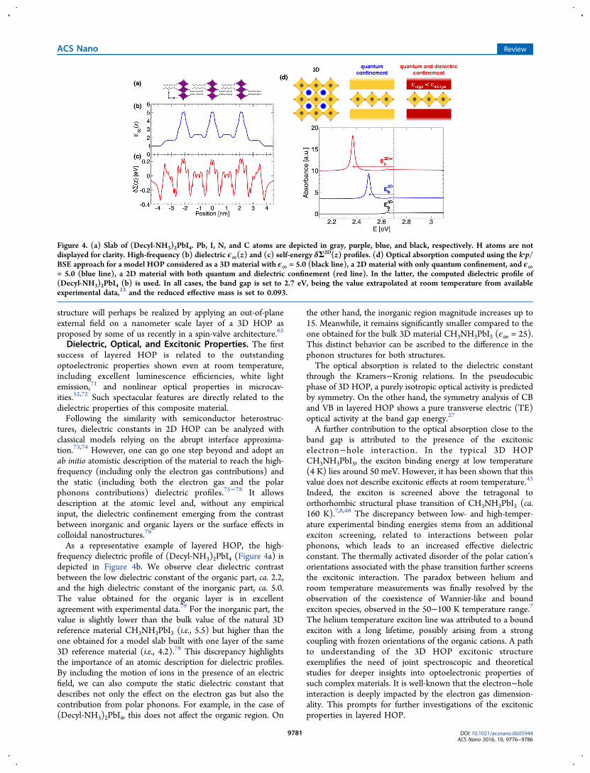
As a representative example of layered HOP, the high-frequency dielectric profile of (Decyl-NH3)2PbI4 (Figure 4a) isdepicted in Figure 4b. We observe clear dielectric contrastbetween the low dielectric constant of the organic part, ca. 2.2,and the high dielectric constant of the inorganic part, ca. 5.0.The value obtained for the organic layer is in excellentagreement with experimental data.79 For the inorganic part, thevalue is slightly lower than the bulk value of the natural 3Dreference material CH3NH3PbI3 (i.e., 5.5) but higher than theone obtained for a model slab built with one layer of the same3D reference material (i.e., 4.2).78 This discrepancy highlightsthe importance of an atomic description for dielectric profiles.By including the motion of ions in the presence of an electricfield, we can also compute the static dielectric constant thatdescribes not only the effect on the electron gas but also thecontribution from polar phonons. For example, in the case of(Decyl-NH3)2PbI4, this does not affect the organic region. On
the other hand, the inorganic region magnitude increases up to15. Meanwhile, it remains significantly smaller compared to theone obtained for the bulk 3D material CH3NH3PbI3 (ϵ∞ = 25).This distinct behavior can be ascribed to the difference in thephonon structures for both structures.The optical absorption is related to the dielectric constant
through the Kramers−Kronig relations. In the pseudocubicphase of 3D HOP, a purely isotropic optical activity is predictedby symmetry. On the other hand, the symmetry analysis of CBand VB in layered HOP shows a pure transverse electric (TE)optical activity at the band gap energy.27
A further contribution to the optical absorption close to theband gap is attributed to the presence of the excitonicelectron−hole interaction. In the typical 3D HOPCH3NH3PbI3, the exciton binding energy at low temperature(4 K) lies around 50 meV. However, it has been shown that thisvalue does not describe excitonic effects at room temperature.45
Indeed, the exciton is screened above the tetragonal toorthorhombic structural phase transition of CH3NH3PbI3 (ca.160 K).7,8,48 The discrepancy between low- and high-temper-ature experimental binding energies stems from an additionalexciton screening, related to interactions between polarphonons, which leads to an increased effective dielectricconstant. The thermally activated disorder of the polar cation’sorientations associated with the phase transition further screensthe excitonic interaction. The paradox between helium androom temperature measurements was finally resolved by theobservation of the coexistence of Wannier-like and boundexciton species, observed in the 50−100 K temperature range.7
The helium temperature exciton line was attributed to a boundexciton with a long lifetime, possibly arising from a strongcoupling with frozen orientations of the organic cations. A pathto understanding of the 3D HOP excitonic structureexemplifies the need of joint spectroscopic and theoreticalstudies for deeper insights into optoelectronic properties ofsuch complex materials. It is well-known that the electron−holeinteraction is deeply impacted by the electron gas dimension-ality. This prompts for further investigations of the excitonicproperties in layered HOP.
Figure 4. (a) Slab of (Decyl-NH3)2PbI4. Pb, I, N, and C atoms are depicted in gray, purple, blue, and black, respectively. H atoms are notdisplayed for clarity. High-frequency (b) dielectric ϵ∞(z) and (c) self-energy δΣ2D(z) profiles. (d) Optical absorption computed using the k·p/BSE approach for a model HOP considered as a 3D material with ϵ∞ = 5.0 (black line), a 2D material with only quantum confinement, and ϵ∞= 5.0 (blue line), a 2D material with both quantum and dielectric confinement (red line). In the latter, the computed dielectric profile of(Decyl-NH3)2PbI4 (b) is used. In all cases, the band gap is set to 2.7 eV, being the value extrapolated at room temperature from availableexperimental data,23 and the reduced effective mass is set to 0.093.
ACS Nano Review
DOI: 10.1021/acsnano.6b05944ACS Nano 2016, 10, 9776−9786
9781
In semiconductors or insulators, the standard approachaccounting for electron−hole interaction relies on the use ofthe BSE built on the monoelectronic states computed at theDFT level or, even better, at the DFT+GW level.80 Indeed, inmany-body perturbation theory, the energy corresponding to asingle-particle removal or addition, that is, the quasiparticleenergy, ϵQP, is obtained from the GW self-energy operator inwhich the exchange-correlation effects are contained throughthe one-electron Green function, G, and the screening of theCoulomb interaction, W
∫ πΣ ′ ϵ = ′
′ − ′ ′ ′δ− ′r r iE
e G r r E E W r r E( , , )d2
( , , ) ( , , )i EQP
(1)
However, in the perturbative BSE/DFT (or DFT+GW)scheme, screening of the electron−hole interaction due toatomic motion is not taken into account. Thus, BSE is morerelevant at low temperature where, for example, cation motionsare expected to be frozen. Moreover, from a technical point ofview, the DFT+GW+BSE scheme is computationally heavy. Infact, it is roughly 100 times more numerically demandingcompared to an equivalent standard DFT calculations. TheDFT+GW scheme including SOC has been applied on severaloccasions to 3D HOP.60,62 More recently, Bokdam et al. usedthe same DFT+GW+BSE scheme with a refined description ofthe one-electron energies.81 Unfortunately, for complexmaterials such as layered HOP, which have a large number ofatoms per unit cell as compared to classical semiconductors,current computational resources are generally not sufficient toafford full DFT+GW+BSE level of theory. Concerning the issueof the band gap, Fraccarollo et al. recently proposed an additivescheme where SOC and GW corrections are includedseparately.82 Here, to simulate excitonic effects in layeredHOP, we suggest the use of a semiempirical framework, such asthe k·p model combined with ab initio calculations.In the literature, the enhanced exciton binding energy of
layered HOP is mainly attributed to dielectric confinementeffects.73,74 This is the case of a pioneering contribution byMuljarov et al.,74 where the exciton binding energies werecalculated using a classical resolution of the BSE. Unfortunately,this approach relied on an abrupt dielectric profile, andnecessary parameters were fitted to experimental data obtainedfrom bulk 3D HOP. Moreover, to avoid nonphysicaldivergences related to abrupt dielectric interfaces,76 an artificialtransitional layer at the interface between the organic andinorganic parts had to be considered.74 By outlining a schemeallowing for the computation of a DFT-based dielectric profile,we herein propose an alternative strategy to model absorptionproperties, including excitonic effects, of 3D and layered HOP.Starting from a reference 3D HOP, the 2D band gap can be
estimated from theoretical calculations by using the followingdecomposition:
δ δ≈ + Σ + + ΣE E Eg g,DFT3D 3D
g,DFT2D 2D
(2)
where Eg,DFT3D + Σ3D is the 3D band gap, including the self-
energy correction. δEg,DFT2D accounts for the effects of quantum
confinement and lattice distortions occurring in the 2Dmaterial. Thus, Eg,DFT
3D + Σ3D + δEg,DFT2D is the 2D band gap, in
principle, available from DFT calculations. However, band gapsare usually not well-reproduced by plain DFT calculations. Ifmore accurate strategies such as GW corrections are out ofreach, one might use an experimentally determined gap or rely
on the use of hybrid functionals instead. Last, δΣ2D containsadditional corrections related to dielectric confinement.Self-energy corrections can be computed for monoelectronic
states near the band gap starting from the dielectric profile:
∫δπ
Σ = −∞
→ze
V q z z V q z z q q( )4
( ( , , ) ( , , )) dz z00
00 bulk 0 0
(3)
where e0 is a test charge at position z0 and V and Vbulk are theelectrostatic potential in the heterostructure and in the bulk,respectively. Back to GW, δΣ(z0) is equivalent to the one-particle potential profile acting on the test charge. V is thenobtained by solving the inhomogeneous Poisson equationincluding the dielectric constant profile ϵ(z):
δ
∂∂
ϵ ∂∂
− ϵ
= − −
∞ ∞⎜ ⎟⎛⎝
⎞⎠z
zz
V q z z q z V q z z
e z z
( ) ( ( , , )) ( ) ( , , )
( )
02
0
0 0 (4)
A detailed description of the procedure is found in refs 76 and78. The example of (Decyl-NH3)2PbI4 in Figure 4c displays theself-energy profile δΣ(z) computed according to the dielectricprofile ϵ∞(z). At the position of the inorganic sheet, the self-energy correction is about +0.2 eV and 10 times less than +0.02eV for the organic part. The semiclassical evaluation of δΣ2D,for both the CB and the VB states, can be obtained bycomputing the following integrals
∫δ δ ρΣ = Σ z z z( ) ( )dCB(VB)2D 2D
CB(VB) (5)
Here ρCB(VB)(z) is the electronic density profile for the CB(VB) state. The integral is computed over a unit cell, taking thecentral part of δΣ2D(z). We then obtain the total band gapcorrection δΣ2D = δΣCB
2D + δΣVB2D and deduce the band gap Eg
from eq 2.Finally, to compute the full absorption spectrum including
excitonic effects, we still need to include the electron−holeinteraction. Here, we provide a brief description of theapproach that will be described at more length elsewhere. Inshort, it can be implemented semiempirically by solving theBSE based on the work by Chuang et al.,83 considering z = z0 =0 due to the 2D character of the material of interest. TheGreen’s function of the exciton is solved according to eq 19 ofref 83. The optical susceptibility is computed using eq 14 of thesame publication. The effective mass approximation is used forthe energies (eq 11 of ref 83). Those can be evaluated from thecomputed band structure. Corresponding wave functions, givenin 8a and 8b of ref 83, are also deduced from the DFT-computed electron densities at the center of the BZ. Thisscheme, in principle, calculates the electron−hole Coulombicinteraction without any experimental input. In the case oftypical layered HOP, evaluation of GW corrections is out ofreach due to large system size. Subsequently, we can rely on theexperimental data to appraise these quantities. Using again(Decyl-NH3)2PbI4 as an example, we extrapolate theexperimental band gap of 2.88 eV recorded at 1.6 K to 2.7eV at room temperature from ref 23.In order to demonstrate the dimensionality and dielectric
effects, we use different ingredients for a 3D perovskitestructure (Figure 4d, black line). The optical absorption isenhanced at the exciton resonance, and an exciton bindingenergy of 50 meV is computed when choosing a reducedeffective mass of 0.093, a value consistent with magneto-
ACS Nano Review
DOI: 10.1021/acsnano.6b05944ACS Nano 2016, 10, 9776−9786
9782

absorption measurements.8 In a second step, we restore the 2Dcharacter of (Decyl-NH3)2PbI4 but do not take into account thedielectric properties as computed in Figure 4c. Here, thespecific effect of quantum confinement on the exciton isevidenced, as shown in Figure 4d (blue line). As expected whengoing from a 3D to 2D structure, the exciton binding energyincreases from 50 to 200 meV. When further including thedielectric confinement contribution, a large exciton bindingenergy of 330 meV is predicted (Figure 4d, red line), in fairagreement with available experimental data.23 These threerepresentative calculations illustrate the relative impacts ofquantum and dielectric confinements. We emphasize that anaccurate description of excitonic properties cannot avoid theprecise delineation of the dielectric contrast.
CONCLUSIONThe 3D HOP are current photovolatic superstars. Superbperformances have motivated intense investigations and shedlight on their structural, electronic, and optical properties.Meanwhile, 2D HOP, that used to be the most popularmembers of the family, have been in the shadow of this suddensuccess. However, they are coming back thanks to better photo-and environmental stability in solar cells and attractive light-emission properties. Furthermore, compared to their 3Dcounterparts, they represent a greater playground for chemiststo investigate.In this review, we outline a systematic comparison of the
structural, electronic, and optical properties of the 3D HOP andtheir 2D layered analogues. In both cases, SOC has a dramaticimpact on the conduction bands, while it typically modifies thevalence band in conventional semiconductors. A specific featureof layered materials is their quantum-well-like behavior thatapproaches a type I quantum confinement, however, withoutthe superlattice effects. These composite structures are alsocharacterized by strongly anisotropic electronic, optical, andcharge carrier transport properties. Similarly to the referencepseudocubic Pm3 m phase already established for 3D HOP,here, we introduce the hypothetical D4h structure, which can beused to rationalize the properties of layered HOP. For instance,a comparable Brillouin zone folding can be considered tofacilitate analysis of structure/property relationships. Finally, wesurvey dielectric and excitonic properties of layered 2D. To thatend, we propose an original theoretical treatment based on anab initio description to supersede the usual DFT+GW+BSEtreatment that cannot be applied to layered HOP due tocurrently intractable computational cost. The former also allowsfor a detailed description at the atomistic level, the interface,and surface effects, however, at a greatly reduced computationalcost.The HOP family still has an enormous potential for various
optoelectronic applications, yet further progress requiresintense investigations. Over the last 2 years, our understandingof 3D HOP properties has made a breakthrough thanks to thepossibility of growing large monocrystals. The similar crystalengineering advance of layered HOP would also greatly benefitthe field. In particular, it would allow for analysis of structuresand phase transitions by enabling many spectroscopic studies(IR, Raman, Brillouin, neutron scattering, etc.). It would alsoconfirm or overturn the presence of the Rashba effect that, tothis moment, has not been observed in either layered or 3DHOP. The 3D structures are very constraining regarding thesize of the cation, leading to severe restrictions over the choiceof the organic moiety. The situation is different with 2D HOP,
where chemical engineering can follow many paths that haveyet to be discovered. The wealth of HOP is not restricted to 3Dand 2D systems. In this tremendous playground, manydimensions are present. For instance, among those verypromising features are delivered by 3D/2D structures, wherethe inorganic sheet counts more than one layer of octahedra.
AUTHOR INFORMATIONCorresponding Authors*E-mail: [email protected].*E-mail: [email protected] authors declare no competing financial interest.
ACKNOWLEDGMENTSThe work at FOTON is supported by Agence Nationale pour laRecherche (SNAP and SuperSansPlomb projects) and wasperformed using HPC resources from GENCI-CINES/IDRISGrant 2016-c2012096724. The work at ISCR is supported byAgence Nationale pour la Recherche (TRANSHYPEROproject). J.E.’s work is supported by the Fondation d’entreprisesbanque Populaire de l’Ouest under Grant PEROPHOT 2015.The work at Los Alamos National Laboratory (LANL) wassupported by LANL LDRD program and was partiallyperformed at the Center for Nonlinear Studies and at theCenter for Integrated Nanotechnologies, a U.S. Department ofEnergy, Office of Science user facility. The Groningen teamwould like to acknowledge funding from European ResearchCouncil (ERC Starting Grant “Hy-SPOD” No. 306983) and bythe Foundation for Fundamental Research on Matter (FOM),which is part of The Netherlands Organization for ScientificResearch (NWO), under the framework of the FOM FocusGroup “Next Generation Organic Photovoltaics”. ICN2acknowledges support from the Severo Ochoa Program(MINECO, Grant SEV-2013-0295). This project receivedfunding from the European Union's Horizon 2020 researchand innovation programme under the grant agreement no.687008. The information and views set out in this publicationare those of the authors and do not necessarily reflect theofficial opinion of the European Union. Neither the EuropeanUnion institutions and bodies nor any person acting on theirbehalf may be held responsible for the use which may be madeof the information contained therein.
VOCABULARYPerovskite, structure similar to the original perovskite mineralCaTiO3 of general stoichiometry ABX3 (respectively, A′2BX4)for 3D (respectively, 2D monolayered materials), where A andA′ are inorganic or organic cations, B is a metallic cation, and Xis an anion; Brillouin zone, primitive cell in the reciprocalspace; Quantum well, 2D confined structure in which energylevels become discrete; Rashba effect, energy splittingoccurring under the simultaneous presence of time-reversalsymmetry and noncentrosymmetric structure, and enhanced bya strong spin−orbit coupling; Self-energy, many-bodycorrection to a particle energy due to its interaction with therest of the system; Exciton, neutral bound state of a systemwhich can be related to an electron−hole pair created from theabsorption of a photon; Ruddlesden−Popper perovskite, ageneral crystal structure of the form An−1A′2BnX3n+1, where n =1 correspond to a 2D monolayered perovskite and n = ∞ to a3D perovskite
ACS Nano Review
DOI: 10.1021/acsnano.6b05944ACS Nano 2016, 10, 9776−9786
9783

REFERENCES(1) Kojima, A.; Teshima, K.; Shirai, T.; Miyasaka, T. OrganometalHalide Perovskites as Visible-Light Sensitizers for Photovoltaic Cells. J.Am. Chem. Soc. 2009, 131, 6050−6051.(2) Lee, M. M.; Teuscher, J.; Miyasaka, T.; Murakami, T. N.; Snaith,H. J. Efficient Hybrid Solar Cells Based on Meso-SuperstructuredOrganometal Halide Perovskites. Science 2012, 338, 643−647.(3) Kim, H.-S.; Lee, C.-R.; Im, J.-H.; Lee, K.-B.; Moehl, T.;Marchioro, A.; Moon, S.-J.; Humphry-Baker, R.; Yum, J.-H.; Moser, J.E.; Gratzel, M.; Park, N.-G. Lead Iodide Perovskite Sensitized All-Solid-State Submicron Thin Film Mesoscopic Solar Cell withEfficiency Exceeding 9%. Sci. Rep. 2012, 2, 591.(4) Burschka, J.; Pellet, N.; Moon, S.-J.; Humphry-Baker, R.; Gao, P.;Nazeeruddin, M. K.; Gratzel, M. Sequential Deposition as a Route toHigh-Performance Perovskite-Sensitized Solar Cells. Nature 2013,499, 316−319.(5) Liu, M.; Johnston, M. B.; Snaith, H. J. Efficient PlanarHeterojunction Perovskite Solar Cells by Vapour Deposition. Nature2013, 501, 395−398.(6) Nie, W.; Tsai, H.; Asadpour, R.; Blancon, J.-C.; Neukirch, A. J.;Gupta, G.; Crochet, J. J.; Chhowalla, M.; Tretiak, S.; Alam, M. A.;Wang, H.-L.; Mohite, A. D. High-Efficiency Solution-ProcessedPerovskite Solar Cells With Millimeter-Scale Grains. Science 2015,347, 522−525.(7) Fang, H.-H.; Raissa, R.; Abdu-Aguye, M.; Adjokatse, S.; Blake, G.R.; Even, J.; Loi, M. A. Photophysics of Organic-Inorganic HybridLead Iodide Perovskite Single Crystals. Adv. Funct. Mater. 2015, 25,2378−2385.(8) Miyata, A.; Mitioglu, A.; Plochocka, P.; Portugall, O.; Wang, J. T.-W.; Stranks, S. D.; Snaith, H. J.; Nicholas, R. J. Direct Measurement ofthe Exciton Binding Energy and Effective Masses for Charge Carriersin Organic-Inorganic Tri-Halide Perovskites. Nat. Phys. 2015, 11,582−588.(9) Bi, D.; Tress, W.; Dar, M. I.; Gao, P.; Luo, J.; Renevier, C.;Schenk, K.; Abate, A.; Giordano, F.; Correa Baena, J.-P.; Decoppet, J.-D.; Zakeeruddin, S. M.; Nazeeruddin, M. K.; Gratzel, M.; Hagfeldt, A.Efficient Luminescent Solar Cells Based on Tailored Mixed-CationPerovskites. Sci. Adv. 2016, 2, e1501170.(10) Saliba, M.; Matsui, T.; Seo, J.-Y.; Domanski, K.; Correa-Baena,J.-P.; Nazeeruddin, M. K.; Zakeeruddin, S. M.; Tress, W.; Abate, A.;Hagfeldt, A.; Gratzel, M. Cesium-Containing Triple Cation PerovskiteSolar Cells: Improved Stability, Reproducibility and High Efficiency.Energy Environ. Sci. 2016, 9, 1989−1997.(11) http://www.nrel.gov/ncpv/images/efficiency_chart.jpg (Ac-cessed August 2016).(12) Chen, W.; Wu, Y.; Yue, Y.; Liu, J.; Zhang, W.; Yang, X.; Chen,H.; Bi, E.; Ashraful, I.; Gratzel, M.; et al. Efficient and Stable Large-Area Perovskite Solar Cells With Inorganic Charge Extraction Layers.Science 2015, 350, 944−948.(13) Li, X.; Bi, D.; Yi, C.; Decoppet, J.-D.; Luo, J.; Zakeeruddin, S.M.; Hagfeldt, A.; Gratzel, M. A Vacuum Flash-Assisted SolutionProcess for High-Efficiency Large-Area Perovskite Solar Cells. Science2016, 353, 58.(14) Razza, S.; Di Giacomo, F.; Matteocci, F.; Cina, L.; Palma, A. L.;Casaluci, S.; Cameron, P.; D’Epifanio, A.; Licoccia, S.; Reale, A.;Brown, T. M.; Di Carlo, A. Perovskite Solar Cells and Large AreaModules (100 cm2) Based on an Air Flow-Assisted PbI2 Blade CoatingDeposition Process. J. Power Sources 2015, 277, 286−291.(15) Babayigit, A.; Ethirajan, A.; Muller, M.; Conings, B. Toxicity ofOrganometal Halide Perovskite Solar Cells. Nat. Mater. 2016, 15,247−251.(16) Chen, P.-Y.; Qi, J.; Klug, M. T.; Dang, X.; Hammond, P. T.;Belcher, A. M. Environmentally Responsible Fabrication of EfficientPerovskite Solar Cells from Recycled Car Batteries. Energy Environ. Sci.2014, 7, 3659−3665.(17) Chen, P.-Y.; Qi, J.; Klug, M. T.; Dang, X.; Hammond, P. T.;Belcher, A. M. Response to the Comments on “EnvironmentallyResponsible Fabrication of Efficient Perovskite Solar Cells fromRecycled Car Batteries” by Po-Yen Chen, Jifa Qi, Matthew T. Klug,
Xiangnan Dang, Paula T. Hammond, and Angela M. Belcher publishedin Energy Environ. Sci. in 2014. Energy Environ. Sci. 2015, 8, 1618−1625.(18) Huang, W.; Manser, J. S.; Kamat, P. V.; Ptasinska, S. Evolutionof Chemical Composition, Morphology, and Photovoltaic Efficiency ofCH3NH3PbI3 Perovskite under Ambient Conditions. Chem. Mater.2016, 28, 303−311.(19) Nie, W.; Blancon, J.-C.; Neukirch, A. J.; Appavoo, K.; Tsai, H.;Chhowalla, M.; Alam, M. A.; Sfeir, M. Y.; Katan, C.; Even, J.; Tretiak,S.; Crochet, J. J.; Gupta, A.; Mohite, A. D. Light-ActivatedPhotocurrent Degradation and Self-Healing in Perovskite SolarCells. Nat. Commun. 2016, 7, 11574.(20) Mitzi, D. B.; Wang, S.; Feild, C. A.; Chess, C. A.; Guloy, A. M.Conducting Layered Organic-inorganic Halides Containing < 110>-Oriented Perovskite Sheets. Science 1995, 267, 1473−1476.(21) Kagan, C. R.; Mitzi, D. B.; Dimitrakopoulos, C. D. Organic-Inorganic Hybrid Materials as Semiconducting Channels in Thin-FilmField-Effect Transistors. Science 1999, 286, 945−947.(22) Mitzi, D. B. Synthesis, Structure, and Properties of Organic-Inorganic Perovskites and Related Materials. Progress in InorganicChemistry; Wiley, 1999; Vol. 48, pp 1−121.(23) Ishihara, T.; Takahashi, J.; Goto, T. Optical Properties Due toElectronic Transitions in Two-Dimensional Semiconductors(CnH2n+1NH3)2PbI4. Phys. Rev. B: Condens. Matter Mater. Phys. 1990,42, 11099−11107.(24) Goto, T.; Makino, H.; Yao, T.; Chia, C. H.; Makino, T.; Segawa,Y.; Mousdis, G. A.; Papavassiliou, G. C. Localization of TripletExcitons and Biexcitons in the Two-Dimensional Semiconductor(CH3C6H4CH2NH3)2PbBr4. Phys. Rev. B: Condens. Matter Mater. Phys.2006, 73, 115206.(25) Mitzi, D. B.; Dimitrakopoulos, C. D.; Kosbar, L. L. StructurallyTailored Organic-Inorganic Perovskites: Optical Properties andSolution-Processed Channel Materials for Thin-Film Transistors.Chem. Mater. 2001, 13, 3728−3740.(26) Sourisseau, S.; Louvain, N.; Bi, W.; Mercier, N.; Rondeau, D.;Boucher, J.-Y.; Buzare, F.; Legein, C. Reduced Band Gap HybridPerovskites Resulting from Combined Hydrogen and HalogenBonding at the Organic-Inorganic Interface. Chem. Mater. 2007, 19,600−607.(27) Even, J.; Pedesseau, L.; Dupertuis, M.-A.; Jancu, J.-M.; Katan, C.Electronic Model for Self-Assembled Hybrid Organic/PerovskiteSemiconductors: Reverse Band Edge Electronic States Ordering andSpin-Orbit Coupling. Phys. Rev. B: Condens. Matter Mater. Phys. 2012,86, 205301.(28) Even, J.; Pedesseau, L.; Katan, C. Understanding QuantumConfinement of Charge Carriers in Layered 2D Hybrid Perovskites.ChemPhysChem 2014, 15, 3733−3741.(29) Pedesseau, L.; Jancu, J.-M.; Rolland, A.; Deleporte, E.; Katan, C.;Even, J. Electronic Properties of 2D and 3D Hybrid Organic/InorganicPerovskites for Optoelectronic and Photovoltaic Applications. Opt.Quantum Electron. 2014, 46, 1225−1232.(30) Saparov, B.; Mitzi, D. B. Organic-Inorganic Perovskites:Structural Versatility for Functional Materials Design. Chem. Rev.2016, 116, 4558−4596.(31) Smith, I. C.; Hoke, E. T.; Solis-Ibarra, D.; McGehee, M. D.;Karunadasa, H. I. A Layered Hybrid Perovskite Solar-Cell Absorberwith Enhanced Moisture Stability. Angew. Chem., Int. Ed. 2014, 53,11232−11235.(32) Cao, D. H.; Stoumpos, C. C.; Farha, O. K.; Hupp, J. T.;Kanatzidis, M. G. 2D Homologous Perovskites as Light-AbsorbingMaterials for Solar Cell Applications. J. Am. Chem. Soc. 2015, 137,7843−7850.(33) Dou, L.; Wong, A. B.; Yu, Y.; Lai, M.; Kornienko, N.; Eaton, S.W.; Fu, A.; Bischak, C. G.; Ma, J.; Ding, T.; Ginsberg, N. S.; Wang, L.-W.; Alivisatos, A. P.; Yang, P. Atomically Thin Two-DimensionalOrganic-Inorganic Hybrid Perovskites. Science 2015, 349, 1518−1521.(34) Yaffe, O.; Chernikov, A.; Norman, Z. M.; Zhong, Y.;Velauthapillai, A.; van der Zande, A.; Owen, J. S.; Heinz, T. F.
ACS Nano Review
DOI: 10.1021/acsnano.6b05944ACS Nano 2016, 10, 9776−9786
9784

Excitons in Ultrathin Organic-Inorganic Perovskite Crystals. Phys. Rev.B: Condens. Matter Mater. Phys. 2015, 92, 045414.(35) Tyagi, P.; Arveson, S. M.; Tisdale, W. A. Colloidal OrganohalidePerovskite Nanoplatelets Exhibiting Quantum Confinement. J. Phys.Chem. Lett. 2015, 6, 1911−1916.(36) Protesescu, L.; Yakunin, S.; Bodnarchuk, M. I.; Krieg, F.;Caputo, R.; Hendon, C. H.; Yang, R. X.; Walsh, A.; Kovalenko, M. V.Nanocrystals of Cesium Lead Halide Perovskites (CsPbX3, X = Cl, Br,and I): Novel Optoelectronic Materials Showing Bright Emission withWide Color Gamut. Nano Lett. 2015, 15, 3692−3696.(37) Stoumpos, C. C.; Cao, D. H.; Clark, D. J.; Young, J.; Rondinelli,J. M.; Jang, J. I.; Hupp, J. T.; Kanatzidis, M. G. Ruddlesden-PopperHybrid Lead Iodide Perovskite 2D Homologous Semiconductors.Chem. Mater. 2016, 28, 2852−2867.(38) Tsai, H.; Nie, W.; Blancon, J.-C.; Stoumpos, C. C.; Asadpour,R.; Harutyunyan, B.; Verduzco, R.; Crochet, J. J.; Tretiak, S.;Pedesseau, L.; Even, J.; Alam, M. A.; Gupta, A.; Lou, J.; Ajayan, P.M.; Bedzyk, M. J.; Kanatzidis, M. G.; Mohite, A. D. High-EfficiencyTwo-Dimensional Ruddlesden−Popper Perovskite Solar Cells. Nature2016, 536, 312−316.(39) Even, J.; Pedesseau, L.; Jancu, J.-M.; Katan, C. Importance ofSpin-Orbit Coupling in Hybrid Organic/Inorganic Perovskites forPhotovoltaic Applications. J. Phys. Chem. Lett. 2013, 4, 2999−3005.(40) Mosconi, E.; Amat, A.; Nazeeruddin, M. K.; Gratzel, M.; DeAngelis, F. First-Principles Modeling of Mixed Halide OrganometalPerovskites for Photovoltaic Applications. J. Phys. Chem. C 2013, 117,13902−13913.(41) Brivio, F.; Walker, A. B.; Walsh, A. Structural and ElectronicProperties of Hybrid Perovskites for High-Efficiency Thin-FilmPhotovoltaics from First-Principles. APL Mater. 2013, 1, 042111.(42) Giorgi, G.; Fujisawa, J.-I.; Segawa, H.; Yamashita, K. SmallPhotocarrier Effective Masses Featuring Ambipolar Transport inMethylammonium Lead Iodide Perovskite: A Density FunctionalAnalysis. J. Phys. Chem. Lett. 2013, 4, 4213−4216.(43) Hohenberg, P.; Kohn, W. Inhomogeneus Electron Gas. Phys.Rev. 1964, 136, B864−B871.(44) Kohn, W.; Sham, L. J. Self-Consistent Equations IncludingExchange and Correlation Effects. Phys. Rev. 1965, 140, A1133−A1138.(45) Even, J.; Pedesseau, L.; Katan, C. Analysis of Multivalley andMultibandgap Absorption and Enhancement of Free Carriers Relatedto Exciton Screening in Hybrid Perovskites. J. Phys. Chem. C 2014,118, 11566−11572.(46) Katan, C.; Pedesseau, L.; Kepenekian, M.; Rolland, A.; Even, J.Interplay of Spin-Orbit Coupling and Lattice Distortion in MetalSubstituted 3D Tri-Chloride Hybrid Perovskites. J. Mater. Chem. A2015, 3, 9232−9240.(47) Even, J.; Pedesseau, L.; Katan, C.; Kepenekian, M.; Lauret, J.-S.;Sapori, D.; Deleporte, E. Solid-State Physics Perspective on HybridPerovskite Semiconductors. J. Phys. Chem. C 2015, 119, 10161−10177.(48) Even, J. Pedestrian Guide to Symmetry Properties of theReference Cubic Structure of 3D All-Inorganic and Hybrid Perov-skites. J. Phys. Chem. Lett. 2015, 6, 2238−2242.(49) Even, J.; Carignano, M.; Katan, C. Molecular Disorder andTranslation/Rotation Coupling in the Plastic Crystal Phase of HybridPerovskites. Nanoscale 2016, 8, 6222−6236.(50) Salpeter, E. E.; Bethe, H. A. A Relativistic Equation for Bound-State Problems. Phys. Rev. 1951, 84, 1232−1242.(51) Kikuchi, K.; Takeoka, Y.; Rikukawa, M.; Sanui, K. Structure andOptical Properties of Lead Iodide Based Two-Dimensional PerovskiteCompounds Containing Fluorophenethylamines. Curr. Appl. Phys.2004, 4, 599−602.(52) Wei, Y.; Lauret, J.-S.; Galmiche, L.; Audebert, P.; Deleporte, E.Strong Exciton-Photon Coupling in Microcavities Containing NewFluorophenethylamine Based Perovskite Compounds. Opt. Express2012, 20, 10399−10405.(53) Billing, D. G.; Lemmerer, A. Synthesis, Characterization andPhase Transitions in the Inorganic-Organic Layered Perovskite-Type
Hybrids [(CnH2n+1NH3)2PbI4], n = 4, 5 and 6. Acta Crystallogr., Sect. B:Struct. Sci. 2007, 63, 735−747.(54) Takahashi, Y.; Obara, R.; Nakagawa, K.; Nakano, M.; Tokita, J.-y.; Inabe, T. Tunable Charge Transport in Soluble Organic-InorganicHybrid Semiconductors. Chem. Mater. 2007, 19, 6312−6316.(55) Mitzi, D. B. Synthesis, Crystal Structure, and Optical andThermal Properties of (C4H9NH3)2MI4 (M = Ge, Sn, Pb). Chem.Mater. 1996, 8, 791−800.(56) Lemmerer, A.; Billing, D. G. Synthesis, Characterization andPhase Transitions of the Inorganic-Organic Layered Perovskite-TypeHybrids [(CnH2n+1NH3)2PbI4], n = 7, 8, 9 and 10. Dalton Trans. 2012,41, 1146−1157.(57) Kamminga, M. E.; Fang, H.-H.; Filip, M. R.; Giustino, F.; Baas,J.; Blake, G. R.; Loi, M. A.; Palstra, T. T. M. Confinement Effects inLow-Dimensional Lead Iodide Perovskite Hybrids. Chem. Mater. 2016,28, 4554−4562.(58) Knutson, J. L.; Martin, J. D.; Mitzi, D. B. Tuning the Band Gapin Hybrid Tin Iodide Perovskite Semiconductors Using StructuralTemplating. Inorg. Chem. 2005, 44, 4699−4705.(59) Filip, M. R.; Eperon, G. E.; Snaith, H. J.; Giustino, F. StericEngineering of Metal-Halide Perovskites with Tunable Optical BandGaps. Nat. Commun. 2014, 5, 5757.(60) Even, J.; Pedesseau, L.; Jancu, J.-M.; Katan, C. DFT and k·pModelling of the Phase Transitions of Lead and Tin HalidePerovskites for Photovoltaic Cells. Phys. Status Solidi RRL 2014, 8,31−35.(61) Kim, M.; Im, J.; Freeman, A. J.; Ihm, J.; Jin, H. Switchable S = 1/2 and J = 1/2 Rashba bands in Ferroelectric Halide Perovskites. Proc.Natl. Acad. Sci. U. S. A. 2014, 111, 6900−6904.(62) Brivio, F.; Butler, K. T.; Walsh, A.; van Schilfgaarde, M.Relativistic Quasiparticle Self-Consistent Electronic Structure ofHybrid Halide Perovskite Photovoltaic Absorbers. Phys. Rev. B:Condens. Matter Mater. Phys. 2014, 89, 155204.(63) Amat, A.; Mosconi, E.; Ronca, E.; Quarti, C.; Umari, P.;Nazeeruddin, M. K.; Gratzel, M.; De Angelis, F. Cation-Induced Band-Gap Tuning in Organohalide Perovskites: Interplay of Spin-OrbitCoupling and Octahedra Tilting. Nano Lett. 2014, 14, 3608−3616.(64) Stroppa, A.; Di Sante, D.; Barone, P.; Bokdam, M.; Kresse, G.;Franchini, C.; Whangbo, M.-H.; Picozzi, S. Tunable FerroelectricPolarization and its Interplay with Spin-Orbit Coupling in Tin IodidePerovskites. Nat. Commun. 2014, 5, 5900.(65) Kepenekian, M.; Robles, R.; Katan, C.; Sapori, D.; Pedesseau, L.;Even, J. Rashba and Dresselhaus Effects in Hybrid Organic-InorganicPerovskites: From Basics to Devices. ACS Nano 2015, 9, 11557−11567.(66) Braun, M.; Frey, W. Crystal Structure of Bis(benzylammonium)Lead Tetrachloride, (C7H7NH3)2PbCl4. Z. Kristallogr. New Cryst.Struct. 1999, 214, 331−332.(67) Liao, W.-Q.; Zhang, Y.; Hu, C.-L.; Mao, J.-G.; Ye, H.-Y.; Li, P.-F.; Huang, S. D.; Xiong, R.-G. A Lead-Halide Perovskite MolecularFerroelectric Semiconductor. Nat. Commun. 2015, 6, 7338.(68) Daub, M.; Hillebrecht, H. Synthesis, Single-Crystal Structureand Characterization of (CH3NH3)2Pb(SCN)2I2. Angew. Chem., Int.Ed. 2015, 54, 11016−11017.(69) Ganose, A. M.; Savory, C. N.; Scanlon, D. O. (CH3NH3)2Pb-(SCN)2I2: A More Stable Structural Motif for Hybrid HalidePhotovoltaics? J. Phys. Chem. Lett. 2015, 6, 4594−4598.(70) Xiao, Z.; Meng, W.; Saparov, B.; Duan, H.-S.; Wang, C.; Feng,C.; Liao, W.; Ke, W.; Zhao, D.; Wang, J.; Mitzi, D. B.; Yan, Y.Photovoltaic Properties of Two-Dimensional (CH3NH3)2Pb(SCN)2I2Perovskite: A Combined Experimental and Density Functional TheoryStudy. J. Phys. Chem. Lett. 2016, 7, 1213−1218.(71) Dohner, E. R.; Jaffe, A.; Bradshaw, L. R.; Karunadasa, H. I.Intrinsic White-Light Emission from Layered Hybrid Perovskites. J.Am. Chem. Soc. 2014, 136, 13154−13157.(72) Lanty, G.; Brehier, A.; Parashkov, R.; Lauret, J.-S.; Deleporte, E.Strong Exciton-Photon Coupling at Room Temperature in Micro-cavities Containing Two-Dimensional Layered Perovskite Com-pounds. New J. Phys. 2008, 10, 065007.
ACS Nano Review
DOI: 10.1021/acsnano.6b05944ACS Nano 2016, 10, 9776−9786
9785

(73) Kumagai, M.; Takagahara, T. Excitonic and Nonlinear-OpticalProperties of Dielectric Quantum-well Structures. Phys. Rev. B:Condens. Matter Mater. Phys. 1989, 40, 12359.(74) Muljarov, E. A.; Tikhodeev, S. G.; Gippius, N. A. Excitons inSelf-Organized Semiconductor/Insulator Superlattices: PbI-BasedPerovskite Compounds. Phys. Rev. B: Condens. Matter Mater. Phys.1995, 51, 14370−14378.(75) Shi, N.; Ramprasad, R. Dielectric Properties of Ultrathin SiO2Slabs. Appl. Phys. Lett. 2005, 87, 262102.(76) Even, J.; Pedesseau, L.; Kepenekian, M. Electronic Surface Statesand Dielectric Self-Energy Profiles in Colloidal Nanoscale Platelets ofCdSe. Phys. Chem. Chem. Phys. 2014, 16, 25182−25190.(77) Benchamekh, R.; Gippius, N. A.; Even, J.; Nestoklon, M. O.;Jancu, J.-M.; Ithurria, S.; Dubertret, B.; Efros, A. L.; Voisin, P. Tight-Binding Calculations of Image-Charge Effects in Colloidal NanoscalePlatelets of CdSe. Phys. Rev. B: Condens. Matter Mater. Phys. 2014, 89,035307.(78) Sapori, D.; Kepenekian, M.; Pedesseau, L.; Katan, C.; Even, J.Quantum Confinement and Dielectric Profiles of Colloidal Nano-platelets of Halide Inorganic and Hybrid Organic-Inorganic Perov-skites. Nanoscale 2016, 8, 6369−6378.(79) Richards, T. W.; Shipley, J. W. The Dielectric Constants ofTypical Aliphatic and Aromatic Hydrocarbons, Cyclohexane, Cyclo-hexanone, and Cyclohexanol. J. Am. Chem. Soc. 1919, 41, 2002−2012.(80) Hedin, L. New Method for Calculating One-Particle GreensFunction with Application to Electron-Gas Problem. Phys. Rev. 1965,139, A796−A823.(81) Bokdam, M.; Sander, T.; Stroppa, A.; Picozzi, S.; Sarma, D. D.;Franchini, C.; Kresse, G. Role of Polar Phonons in the Photo ExcitedState of Metal Halide Perovskites. Sci. Rep. 2016, 6, 28618.(82) Fraccarollo, A.; Cantatore, V.; Boschetto, G.; Marchese, L.;Cossi, M. Ab Initio Modeling of 2D Layered Organohalide LeadPerovskites. J. Chem. Phys. 2016, 144, 164701.(83) Chuang, S.-L.; Schmitt-Rink, S.; Miller, D. A. B.; Chemla, D. S.Exciton Green’s-Function Approach to Optical Absorption in aQuantum Well with an Applied Electric Field. Phys. Rev. B: Condens.Matter Mater. Phys. 1991, 43, 1500−1509.
ACS Nano Review
DOI: 10.1021/acsnano.6b05944ACS Nano 2016, 10, 9776−9786
9786


![Organometal Halide Perovskite Artificial Synapsesphome.postech.ac.kr/user/pnel/publication/133... · mediated by oxygen defects,[28,29] and low activation energy E a of halide migration](https://static.fdocuments.us/doc/165x107/5f95b6c6097fcd28852a939e/organometal-halide-perovskite-artificial-mediated-by-oxygen-defects2829-and.jpg)