
Characterization of Planar Lead Halide Perovskite Solar Cells by ...
10
Characterization of Planar Lead Halide Perovskite Solar Cells by Impedance Spectroscopy, Open-Circuit Photovoltage Decay, and Intensity-Modulated Photovoltage/Photocurrent Spectroscopy Adam Pockett, † Giles E. Eperon, ‡ Timo Peltola, § Henry J. Snaith, ‡ Alison Walker, § Laurence M. Peter,* ,† and Petra J. Cameron* ,† † Department of Chemistry and § Department of Physics, University of Bath, Bath BA2 7AY, United Kingdom ‡ Clarendon Laboratory, Parks Road, Oxford OX1 3PU, United Kingdom * S Supporting Information ABSTRACT: Thin film lead halide perovskite cells, where the perovskite layer is deposited directly onto a flat titania blocking layer, have reached AM 1.5 efficiencies of over 15%, 1 showing that the mesoporous scaffold used in early types of perovskite solar cells is not essential. We used a variety of techniques to gain a better understanding of thin film perovskite cells prepared by a solution-based method. Twelve cells were studied, which showed AM 1.5 efficiencies of ∼11%. The properties of the cells were investigated using impedance spectroscopy, intensity-modulated photovoltage spectroscopy (IMVS), intensity-modulated photocurrent spectroscopy (IMPS), and open-circuit photovoltage decay (OCVD). Despite the fact that all 12 cells were prepared at the same time under nominally identical conditions, their behavior fell into two distinct groups. One half of the cells exhibited ideality factors of m ≈ 2.5, and the other half showed ideality factors of m ≈ 5. Impedance spectroscopy carried out under illumination at open circuit for a range of intensities showed that the cell capacitance was dominated by the geometric capacitance of the perovskite layer rather than the chemical or diffusion capacitance due to photogenerated carriers. The voltage dependence of the recombination resistance gave ideality factors similar to those derived from the intensity dependence of the open-circuit voltage. The IMVS time constant was determined by the product of the geometric capacitance and the recombination resistance. The two types of cells gave very different OCVD responses. The cells with m ≈ 2.5 showed a persistent photovoltage effect that was absent in the case of the cells with higher ideality factors. The IMPS responses provide evidence of minor efficiency losses by recombination under short-circuit conditions. ■ INTRODUCTION The rapid development of organometal halide perovskite solar cells 2−5 based on CH 3 NH 3 PbI 3 and its analogs continues to set new records in terms of efficiency 6 that already far exceed those for dye-sensitized solar cells or organic photovoltaics. The high open-circuit voltages and high external quantum efficiencies point to unusually slow recombination of electrons and holes in the perovskite absorber layer, with second-order rate constants for uncontacted thin films reported to be four orders lower than the Langevin limit for bimolecular recombination. 7 The reasons for such slow recombination are currently a central topic of discussion, 8−10 and it has been suggested that the formation of ferroelectric domains may lead to spatial separation of electrons and holes. 11,12 It has also been reported that the lead halide perovskites exhibit a photoinduced giant dielectric effect (GDE) with a relaxation time constant in the region of seconds. 13 The high open-circuit voltages (in excess of 1 V) also indicate that the built-in voltage of the junction must be unusually high (>1 V) relative to the band gap of the perovskite (ca. 1.5 eV). Reported band alignments in the TiO 2 |perovskite| spiro-OMeTAD structure 14 suggest that the built-in voltage in the thin perovskite layer could exceed 1.2 V. In principle, electron−hole recombination can occur either in the bulk of the perovskite or at the contacts, which are made using materials that are selective for extraction of electrons (e.g., TiO 2 ) or holes (e.g., spiro-OMeTAD). A number of methods have been used to study electron−hole recombination including transient microwave 9,15,16 and terahertz 9,16,17 meas- urements, photoluminescence, 18 transient absorbance, 7,18 EBIC, 19 photovoltage and photocurrent transients, 20 impe- dance, 21−24 and open-circuit voltage decay. 25 Many of these studies have characterized the properties of perovskite cells fabricated using mesoporous oxide substrates of either TiO 2 or Al 2 O 3 . However, interest is increasingly being focused on planar junction perovskite cells that appear in many instances to operate as p−i−n devices. 19 For this reason we chose to characterize batches of planar perovskite cells using a range of complementary techniques, namely, impedance, intensity- modulated photovoltage spectroscopy (IMVS), intensity- modulated photocurrent spectroscopy (IMPS), open-circuit Received: October 29, 2014 Revised: January 21, 2015 Published: January 21, 2015 Article pubs.acs.org/JPCC © 2015 American Chemical Society 3456 DOI: 10.1021/jp510837q J. Phys. Chem. C 2015, 119, 3456−3465 This is an open access article published under a Creative Commons Attribution (CC-BY) License, which permits unrestricted use, distribution and reproduction in any medium, provided the author and source are cited.
Transcript of Characterization of Planar Lead Halide Perovskite Solar Cells by ...

Characterization of Planar Lead Halide Perovskite Solar Cells byImpedance Spectroscopy, Open-Circuit Photovoltage Decay, andIntensity-Modulated Photovoltage/Photocurrent SpectroscopyAdam Pockett,† Giles E. Eperon,‡ Timo Peltola,§ Henry J. Snaith,‡ Alison Walker,§ Laurence M. Peter,*,†
and Petra J. Cameron*,†
†Department of Chemistry and §Department of Physics, University of Bath, Bath BA2 7AY, United Kingdom‡Clarendon Laboratory, Parks Road, Oxford OX1 3PU, United Kingdom
*S Supporting Information
ABSTRACT: Thin film lead halide perovskite cells, where the perovskite layer isdeposited directly onto a flat titania blocking layer, have reached AM 1.5 efficiencies ofover 15%,1 showing that the mesoporous scaffold used in early types of perovskite solarcells is not essential. We used a variety of techniques to gain a better understanding ofthin film perovskite cells prepared by a solution-based method. Twelve cells were studied,which showed AM 1.5 efficiencies of ∼11%. The properties of the cells were investigatedusing impedance spectroscopy, intensity-modulated photovoltage spectroscopy (IMVS),intensity-modulated photocurrent spectroscopy (IMPS), and open-circuit photovoltagedecay (OCVD). Despite the fact that all 12 cells were prepared at the same time undernominally identical conditions, their behavior fell into two distinct groups. One half of thecells exhibited ideality factors of m ≈ 2.5, and the other half showed ideality factors of m≈ 5. Impedance spectroscopy carried out under illumination at open circuit for a range ofintensities showed that the cell capacitance was dominated by the geometric capacitanceof the perovskite layer rather than the chemical or diffusion capacitance due tophotogenerated carriers. The voltage dependence of the recombination resistance gave ideality factors similar to those derivedfrom the intensity dependence of the open-circuit voltage. The IMVS time constant was determined by the product of thegeometric capacitance and the recombination resistance. The two types of cells gave very different OCVD responses. The cellswith m ≈ 2.5 showed a persistent photovoltage effect that was absent in the case of the cells with higher ideality factors. TheIMPS responses provide evidence of minor efficiency losses by recombination under short-circuit conditions.
■ INTRODUCTION
The rapid development of organometal halide perovskite solarcells2−5 based on CH3NH3PbI3 and its analogs continues to setnew records in terms of efficiency6 that already far exceed thosefor dye-sensitized solar cells or organic photovoltaics. The highopen-circuit voltages and high external quantum efficienciespoint to unusually slow recombination of electrons and holes inthe perovskite absorber layer, with second-order rate constantsfor uncontacted thin films reported to be four orders lower thanthe Langevin limit for bimolecular recombination.7 The reasonsfor such slow recombination are currently a central topic ofdiscussion,8−10 and it has been suggested that the formation offerroelectric domains may lead to spatial separation of electronsand holes.11,12 It has also been reported that the lead halideperovskites exhibit a photoinduced giant dielectric effect(GDE) with a relaxation time constant in the region ofseconds.13 The high open-circuit voltages (in excess of 1 V)also indicate that the built-in voltage of the junction must beunusually high (>1 V) relative to the band gap of the perovskite(ca. 1.5 eV). Reported band alignments in the TiO2|perovskite|spiro-OMeTAD structure14 suggest that the built-in voltage inthe thin perovskite layer could exceed 1.2 V.
In principle, electron−hole recombination can occur either inthe bulk of the perovskite or at the contacts, which are madeusing materials that are selective for extraction of electrons(e.g., TiO2) or holes (e.g., spiro-OMeTAD). A number ofmethods have been used to study electron−hole recombinationincluding transient microwave9,15,16 and terahertz9,16,17 meas-urements, photoluminescence,18 transient absorbance,7,18
EBIC,19 photovoltage and photocurrent transients,20 impe-dance,21−24 and open-circuit voltage decay.25 Many of thesestudies have characterized the properties of perovskite cellsfabricated using mesoporous oxide substrates of either TiO2 orAl2O3. However, interest is increasingly being focused on planarjunction perovskite cells that appear in many instances tooperate as p−i−n devices.19 For this reason we chose tocharacterize batches of planar perovskite cells using a range ofcomplementary techniques, namely, impedance, intensity-modulated photovoltage spectroscopy (IMVS), intensity-modulated photocurrent spectroscopy (IMPS), open-circuit
Received: October 29, 2014Revised: January 21, 2015Published: January 21, 2015
Article
pubs.acs.org/JPCC
© 2015 American Chemical Society 3456 DOI: 10.1021/jp510837qJ. Phys. Chem. C 2015, 119, 3456−3465
This is an open access article published under a Creative Commons Attribution (CC-BY)License, which permits unrestricted use, distribution and reproduction in any medium,provided the author and source are cited.

photovoltage decay (OCPVD), and steady-state photovoltagemeasurements as a function of light intensity. The use of thesesix techniques on a large number of cells allowed us to assessthe consistency of the conclusions.The series of 12 planar perovskite devices could be divided
clearly into two groups on the basis of the intensitydependences of the open-circuit voltage, which correspondedto diode ideality factors that clustered either around ∼2.5 oraround ∼5.0. The high-frequency impedance and intensity-modulated photovoltage (IMVS) responses of the cells weremodeled satisfactorily using a simple lumped RC circuit. At lowfrequencies an additional feature was observed which Juarez-Perez et al.13 attributed to a photoinduced giant dielectriceffect. The influence of the GDE on the low-frequencyimpedance response has been modeled by Bisquert et al.,26
but in this paper the low-frequency feature has not beenincluded in modeling. Substantial information about the cellwas extracted using the simple lumped model at mid and highfrequencies, and we are currently measuring and modeling thelow-frequency feature separately. The results obtained at opencircuit by impedance and IMVS are in good agreement, bothindicating that for open-circuit voltages below 0.9 V, thegeometric capacitance associated with charge in the contactingphases (TiO2 and spiro-OMeTAD) is larger than the chemical(or diffusion) capacitance associated with the buildup ofelectrons and holes in the perovskite absorber, even at thehighest light intensities used here (equivalent to 0.1 Sun). Thevoltage dependence of the recombination resistance gavenonideality factors close to those derived from the intensitydependence of the open-circuit voltage. OCVD also reveals thatsome cells exhibit a persistent photovoltage that extends thedecay time into the region of seconds when the voltage fallsbelow 0.4 V.
■ EXPERIMENTAL SECTIONPerovskite Precursor Preparation. Methylamine iodide
(MAI) was prepared by reacting methylamine, 33 wt % inethanol (Sigma-Aldrich), with hydroiodic acid (HI), 57 wt % inwater (Sigma-Aldrich), at room temperature. HI was addeddropwise while stirring. Upon drying at 100 °C, a white powderwas formed, which was washed with ethanol and driedovernight in a vacuum oven before use.To form the nonstoichiometric CH3NH3PbI3−xClx precursor
solution, methylammonium iodide and lead(II) chloride (98%,Sigma-Aldrich) were dissolved in anhydrous N,N-dimethylfor-mamide (DMF) at a 3:1 molar ratio of MAI to PbCl2, with finalconcentrations of 0.88 M lead chloride and 2.64 Mmethylammonium iodide. This solution is stored under a drynitrogen atmosphere.Substrate Preparation. Devices were fabricated on
fluorine-doped tin oxide (FTO) coated glass (Pilkington, 7 Ω□−1). To prevent shunting upon contact with measurementpins, FTO was removed from regions under the anode contactby etching with 2 M HCl and zinc powder. Substrates werethen cleaned sequentially in 2% Hellmanex detergent, acetone,propan-2-ol, and oxygen plasma. A hole-blocking layer ofcompact TiO2 was deposited by spin coating a mildly acidicsolution of titanium isopropoxide in anhydrous ethanol (350μL in 5 mL of ethanol with 0.013 M HCl) and annealed at 500°C for 30 min. Spin coating was carried out at 2000 rpm for 60s.Perovskite Solar Cell Fabrication. A total of 12 cells was
fabricated in groups of 3 cells on one substrate, each with a
pixel area of 0.15 cm2. To form the perovskite layer, thenonstoichiometric precursor was spin coated on the substratein a nitrogen-filled glovebox at 2000 rpm for 45 s. After spincoating, the films were left to dry at room temperature in theglovebox for 30 min to allow slow solvent evaporation. Theywere then annealed on a hot plate in the glovebox at 90 °C for180 min and subsequently at 120 °C for 15 min.A hole-transporting layer was then deposited via spin coating
a 0.79 M solution of 2,2′,7,7′-tetrakis(N,N-di-p-methoxyphenyl-amine)-9,9′-spirobifluorene (spiro-OMeTAD) in chloroben-zene, with additives of lithium bis(trifluoromethanesulfonyl)-imide (0.0184 M) and 4-tert-butylpyridine (0.0659 M). Spincoating was carried out at 2000 rpm for 45 s. Devices were thenleft overnight in air for the spiro-OMeTAD to dope viaoxidation. Finally, gold electrodes were thermally evaporatedunder a vacuum of ∼10−6 Torr at a rate of ∼0.1 nm s−1 tocomplete the devices.
Solar Cell Characterization. The current density−voltage(J−V) curves were measured (2400 Series SourceMeter,Keithley Instruments) under simulated AM 1.5 sunlight at100 mW cm−2 irradiance generated by an Abet Class AAB sun2000 simulator, with the intensity calibrated with an NRELcalibrated KG5-filtered Si reference cell. The mismatch factorwas calculated to be 1.2% between 400 and 1100 nm. The solarcells were masked with a metal aperture to define the activearea, typically 0.0625 cm−2, and measured in a light-tightsample holder to minimize any edge effects.The cells were stored in a nitrogen glovebox between
measurements to minimize degradation. Open-circuit voltageswere measured as a function of light intensity using a 625 nmlight-emitting diode (LED) (Thorlabs MRLED). The incidentphoton flux was controlled using neutral density filters(Edmund Optics) and measured using a calibrated siliconphotodiode (Newport 818-SL with OD3 neutral density filter).All modulated techniques were also carried out withillumination from a 625 nm LED where appropriate (ThorlabsMRLED). Impedance measurements for different illuminationintensities were made at the corresponding open-circuit voltageusing an Autolab PGSTAT30. Impedance measurements werealso made in the dark as a function of applied voltage.Impedance data were fitted using ZView software (ScribnerAssociates). IMVS and IMPS measurements were made using aSolartron 1260 frequency response analyzer (FRA) combinedwith a Thorlabs DC2100 controller (bandwidth 100 kHz)driven by the dc and sine wave output of the FRA. Themodulation depth was set to be 10% of the dc level. Theillumination intensity was varied using calibrated neutraldensity filters. To ensure long-term stability, cells wereilluminated with a single wavelength at intensities of 0.1 Sunand lower. By measuring trends with respect to illuminationintensity we were able to derive significant amounts ofinformation on cell behavior. In the environment solar cellsneed to operate at illumination intensities below 1 Sun;therefore, tests of cell performance at 0.1 Sun can still beconsidered as the working environment for a cell. To correctfor attenuation and phase lag in the modulated light output athigher frequencies, a glass microscope slide was used as a beamsplitter enabling provision of a reference signal for thefrequency response analyzer from a fast p−i−n photodiode.For IMPS, the cell current was measured using a currentamplifier (Femto DLPCA-200). A high-impedance (>1012
ohm) voltage follower was used for IMVS. The bandwidth ofthe system was checked using a fast p−i−n photodiode in place
The Journal of Physical Chemistry C Article
DOI: 10.1021/jp510837qJ. Phys. Chem. C 2015, 119, 3456−3465
3457
of the solar cell. OCVD measurements were made using stepfunction illumination of the cells (625 nm LED; on period 60s). The voltage decay after switching the light off was measuredusing the high-impedance voltage follower amplifier and adigital storage oscilloscope. Care was taken to totally excludestray light.
■ THEORYDiode Ideality Factor. The diode ideality factor, n, is
normally defined in terms of the Shockley diode equation,which describes the dependence of the diode current density, j,on the applied voltage V. Here, jsat is the reverse saturationcurrent
= −j j e( 1)qV nk Tsat
/ B(1)
In theory, n can take different values between 1 and 3,depending on the recombination mechanism27 (Hall ShockleyRead, Sah Noyce Shockley, Auger, etc.), although in some casesanomalously high experimental values of n may point to theexistence of several junctions in a device.28 Here, we are mainlyconcerned with the behavior of perovskite cells underillumination, and so we define a diode ideality factor m usingthe intensity dependence of the open-circuit voltage, whichtakes the form
∂∂
=V
Imk T
qlnoc
0
B
(2)
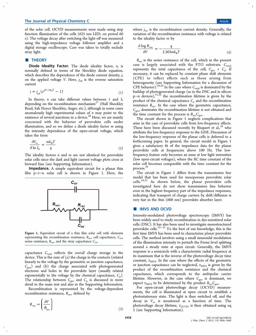
The ideality factors n and m are not identical for perovskitesolar cells since the dark and light current voltage plots cross atforward bias (see Supporting Information).Impedance. A simple equivalent circuit for a planar thin
film p−i−n solar cell is shown in Figure 1. Here, the
capacitance Ctotal reflects the overall charge storage in thedevice. This is the sum of (a) the charge in the contacts (relatedlinearly to the voltage by the geometric or junction capacitance,Cgeo) and (b) the charge associated with photogeneratedelectrons and holes in the perovskite layer (usually relatedexponentially to the voltage by the chemical capacitance, Cμ).The relationship between Cgeo and Cμ is discussed in moredetail in the main text and also in the Supporting Information.Recombination is represented by the voltage-dependent
recombination resistance, Rrec, defined by
= ∂∂
⎛⎝⎜⎜
⎞⎠⎟⎟R
Vjrecrec (3)
where jrec is the recombination current density. Generally, thevariation of the recombination resistance with voltage is relatedto the ideality factor m by
∂∂
= −R
Vqmk T
log2.303
rec
B (4)
Rser is the series resistance of the cell, which in the presentcase is largely associated with the FTO substrate. Ctotalrepresents the total capacitance of the cell, Cgeo + Cμ. Ifnecessary, it can be replaced by constant phase shift elements(CPE) to reflect effects such as those arising fromheterogeneity (see Supporting Information for a discussion ofCPE behavior).29,30 In the case where Ctotal is dominated by thebuildup of photogenerated charge (as in the DSC and in siliconp−n devices),31,32 the recombination lifetime is given by theproduct of the chemical capacitance Cμ and the recombinationresistance Rrec. In the case where the geometric capacitance,Cgeo, dominates the recombination lifetime is not obtained andthe time constant for the process is RrecCgeo.The circuit shown in Figure 1 neglects complications that
arise in the case of perovskite cells from low-frequency effects.These have been discussed recently by Bisquert et al.,26 whoattribute the low-frequency response to the GDE. Discussion ofthe low-frequency response of the planar cells is deferred to aforthcoming paper. In general, the circuit model in Figure 1gives a satisfactory fit of the impedance data for the planarperovskite cells at frequencies above 100 Hz. The low-frequency feature only becomes an issue at low light intensities(low open-circuit voltages), where the RC time constant of thesolar cell becomes comparable with the time constant for theprocess.29
The circuit in Figure 1 differs from the transmission linemodel that has been used for mesoporous perovskite solarcells.10,21 As shown below, the planar perovskite cellsinvestigated here do not show transmission line behavioreven in the highest frequency part of the impedance responses,indicating that transport of charge carriers by drift/diffusion isvery fast in the thin (600 nm) perovskite absorber layer.
■ IMVS AND OCVDIntensity-modulated photovoltage spectroscopy (IMVS) hasbeen widely used to study recombination in dye-sensitized solarcells (DSC). It has also been used to investigate mesostructuredperovskite cells.33−35 To the best of our knowledge, this is thefirst time IMVS has been used to characterize planar perovskitecells. The method involves using a small sinusoidal modulationof the illumination intensity to perturb the Fermi level splittingaround a steady state at open circuit. Generally, the IMVSresponse is a semicircle with a characteristic radial frequency atits maximum that is the inverse of the photovoltage decay timeconstant, τIMVS. In the case where the effects of the geometricor junction capacitance can be neglected, τIMVS is given by theproduct of the recombination resistance and the chemicalcapacitance, which corresponds to the ambipolar carrierlifetime. However, in the case where Cgeo is dominant, weexpect τIMVS to be determined by the product RrecCgeo.For open-circuit photovoltage decay (OCVD) measure-
ments, the cell is illuminated at open circuit to establish aphotostationary state. The light is then switched off, and thedecay in Voc is monitored as a function of time. Thephotovoltage decay lifetime, τOCVD, is then obtained using eq5 (see Supporting Information).
Figure 1. Equivalent circuit of a thin film solar cell with elementsrepresenting the recombination resistance, Rrec, cell capacitance, Ctot,series resistance, Rser, and the stray capacitance Cstr.
The Journal of Physical Chemistry C Article
DOI: 10.1021/jp510837qJ. Phys. Chem. C 2015, 119, 3456−3465
3458
τ = − −− −⎛
⎝⎜⎞⎠⎟
⎛⎝⎜
⎞⎠⎟
k Tq
Vt
Vt
Vt
2 dd
dd
dd
OC OCOCVD
B1 2
OC2
1
(5)
Equation 5 is derived using an approach similar to that ofZaban et al.36 but for the two carrier case where the excesscarrier densities are higher than the doping density of thematerial (see Supporting Information). The second term in eq5 is often omitted, and a satisfactory approximation of thelifetime can be obtained by the first term (see ref 31 for moredetails).If the chemical capacitance of the cell is larger than the
geometric capacitance obtained from eq 5, the decay lifetimecorresponds to the ambipolar carrier lifetime. However, in thecase where the geometric/junction capacitance dominates, weexpect τOCVD to correspond to the RC time constant RrecCgeo.
■ IMPSIn cases where carrier transport is slow, the IMPS response canbe used to measure the delay in collecting carriers at thecontacts. IMPS has been used extensively to study trap-limitedelectron transport in dye-sensitized solar cells.37,38 It has alsobeen used to study mesostructured perovskite solar cells.33
However, in the case of normal p−n or p−i−n solar cellswithout deep trap states, carrier separation is so fast that it ismuch more difficult to measure by IMPS. The high-frequencyIMPS response is dominated in this case by the attenuationarising from the time constant of the solar cell, whichcorresponds to RserCtotal in Figure 1. By contrast, in the caseof mesostructured perovskite solar cells, IMPS may give boththe RC time constant and a time constant due to electrontransport in the mesoporous titania scaffold. IMPS has alsobeen used to characterize charge transfer and recombination insemiconductor−electrolyte contacts.38,39 In this case, themodulated illumination generates a flux of minority carriersinto the surface (e.g., at the semiconductor−solution interface).Once there, the carriers either can be involved in a chargetransfer reaction or may combine with majority carriers. Therelaxation of the minority carrier concentration at the surface bycharge transfer and recombination gives rise to a semicircle inthe complex plane IMPS plot with a radial frequency at themaximum that is equal to the inverse of the relaxation lifetimeτIMPS
−1 = ktrans + krec, The normalized low-frequency interceptof the IMPS plot corresponds to the dc response, and itdepends on the fraction of the minority carriers that make itacross the interface. This charge transfer ef f iciency, ηtrans, is givensimply by the ratio ktrans/(ktrans + krec).
39,40 Here, ktrans and krecare first-order (or pseud- first-order) rate constants for chargetransfer and recombination at short circuit, respectively.
■ RESULTS AND DISCUSSIONCell Efficiencies. Representative IV curves (Figures S1 and
S2) and a summary of the efficiencies of all the cells used in thisstudy are given in the Supporting Information. Five deviceswere studied, each of which contained three pixels, making atotal of 15 solar cells. The cells showed an average efficiency of11.05% at 1 Sun and AM1.5 with a standard deviation of 1.02%(number of samples, n = 14). The two cells presented in mostdetail below had efficiencies of 11.98% (FS43_1) and 9.60%(FB06_1). One of the pixels gave an anomalously lowefficiency and was disregarded, two further pixels degradedduring transport, and the data from them was also not includedin the study.
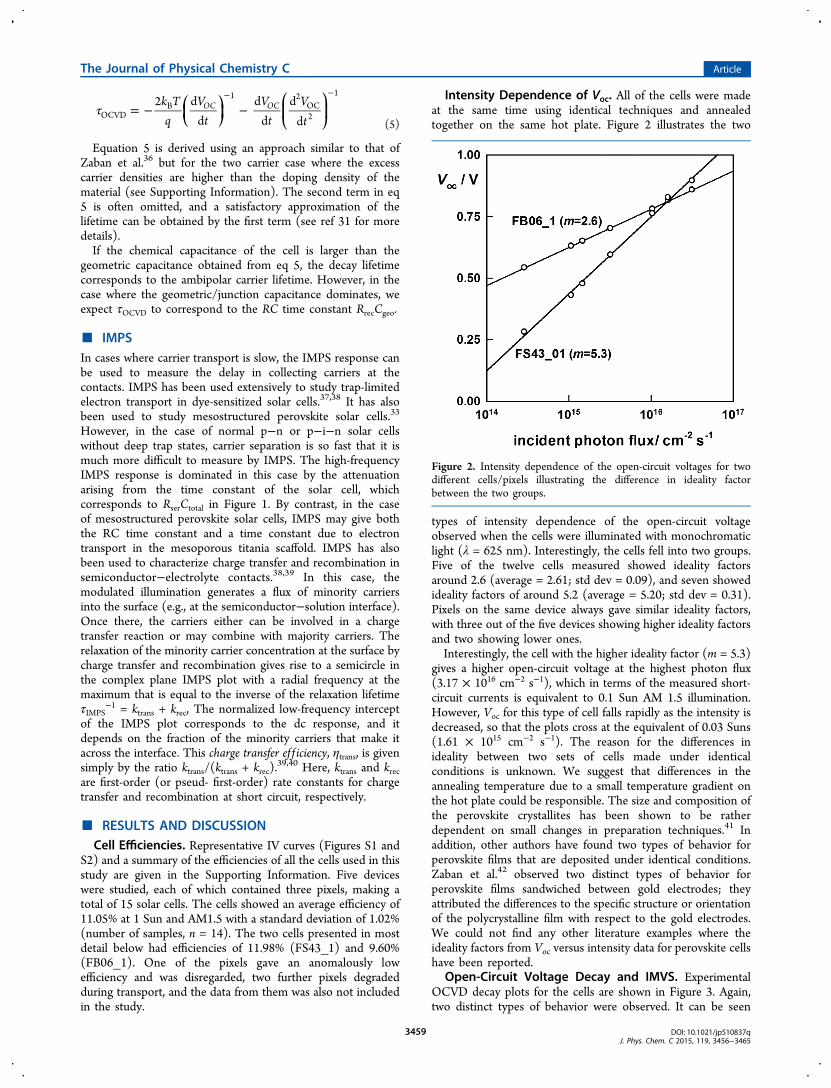
Intensity Dependence of Voc. All of the cells were madeat the same time using identical techniques and annealedtogether on the same hot plate. Figure 2 illustrates the two
types of intensity dependence of the open-circuit voltageobserved when the cells were illuminated with monochromaticlight (λ = 625 nm). Interestingly, the cells fell into two groups.Five of the twelve cells measured showed ideality factorsaround 2.6 (average = 2.61; std dev = 0.09), and seven showedideality factors of around 5.2 (average = 5.20; std dev = 0.31).Pixels on the same device always gave similar ideality factors,with three out of the five devices showing higher ideality factorsand two showing lower ones.Interestingly, the cell with the higher ideality factor (m = 5.3)
gives a higher open-circuit voltage at the highest photon flux(3.17 × 1016 cm−2 s−1), which in terms of the measured short-circuit currents is equivalent to 0.1 Sun AM 1.5 illumination.However, Voc for this type of cell falls rapidly as the intensity isdecreased, so that the plots cross at the equivalent of 0.03 Suns(1.61 × 1015 cm−2 s−1). The reason for the differences inideality between two sets of cells made under identicalconditions is unknown. We suggest that differences in theannealing temperature due to a small temperature gradient onthe hot plate could be responsible. The size and composition ofthe perovskite crystallites has been shown to be ratherdependent on small changes in preparation techniques.41 Inaddition, other authors have found two types of behavior forperovskite films that are deposited under identical conditions.Zaban et al.42 observed two distinct types of behavior forperovskite films sandwiched between gold electrodes; theyattributed the differences to the specific structure or orientationof the polycrystalline film with respect to the gold electrodes.We could not find any other literature examples where theideality factors from Voc versus intensity data for perovskite cellshave been reported.
Open-Circuit Voltage Decay and IMVS. ExperimentalOCVD decay plots for the cells are shown in Figure 3. Again,two distinct types of behavior were observed. It can be seen
Figure 2. Intensity dependence of the open-circuit voltages for twodifferent cells/pixels illustrating the difference in ideality factorbetween the two groups.
The Journal of Physical Chemistry C Article
DOI: 10.1021/jp510837qJ. Phys. Chem. C 2015, 119, 3456−3465
3459

that the cell with m = 2.6 in Figure 2 exhibits a remarkably slowdecay of Voc: the voltage is still 0.4 V after 1 s, and the decay isnot complete even at 10 s. By contrast, the open-circuit voltageof the cell with m = 5.3 decays much more rapidly, falling below0.1 V in only 10 ms. Similar anomalously slow OCVD behaviorhas been reported by Baumann et al.25 for vapor-depositedperovskite cells in which the TiO2 and MeOTAD contacts werereplaced by PC70PCBM and PEDOT:PSS/polyTPD, respec-tively. The authors interpreted the decay in terms of thekinetics of electron−hole recombination and found that therecombination order was between 2 and 3 and that it varieddepending on the illumination intensity the cell was exposed toprior to the decay.The IMVS responses (Figure S8, Supporting Information,
shows representative IMVS data) of the cells measured overtwo decades of light intensity were well-defined semicircles inthe complex plane, and τIMVS was derived from the inverse ofthe radial frequency corresponding to the maximum of theimaginary component.The lifetimes derived from the OCVD plots in Figure 3 and
from the corresponding IMVS measurements on the tworepresentative cells are presented in Figure 4. Details of thesmoothing and fitting procedures used to obtain τOCVD aregiven in the Supporting Information. The reasonable agreementbetween the lifetimes derived by the transient and smallsinusoidal modulation methods indicates that the open-circuitdecays through a set of quasistatic states, at least in the voltagerange preceding the steeper rise in lifetime that can be seen inthe τ plots for both cells. The slopes of the regression fits of theIMVS plots for the two types of cell correspond to m values,which are similar to those derived from the intensitydependence of the open-circuit voltage (cf. Figure 2). It isimportant to note that as the geometric capacitance dominatesthe response of the planar cells (see Supporting Informationdiscussion in the next section), OCVD and IMVS are notmeasuring the time constant for ambipolar recombination. The
relaxation time, τIMVS/τOCVD, instead appears to be dictated bythe product RrecCgeo.The lifetimes measured by IMVS for the two cells were
found to be inversely proportional to the incident light intensityas shown in Figure 5. Remarkably, the lifetimes of the two cellsat the same light intensity are very similar, in spite of the factthat the open-circuit voltages (and presumably therefore theexcess electron and hole concentrations) are quite different. Asshown below, the recombination resistances of the two cellsmeasured by impedance spectroscopy were also very similar
Figure 3. Open-circuit voltage decays for the two types of cell. Notethat the cell with the lower m value in Figure 2 (FB-06_1) exhibits theanomalously slow voltage decay, whereas the voltage of a cell with m =5.3 decays much more rapidly.
Figure 4. Lifetimes (τIMVS and τOCVD) for the two cells derived fromthe open-circuit voltage decay (lines) and from the IMVS response(open circles). Regression fits of the IMVS lifetimes give the values ofm shown in the figure. These are similar to those derived from theintensity dependence of the Voc (see Figure 2).
Figure 5. Intensity dependence of the lifetimes measured by IMVS forthe two cells. The broken line corresponds to a linear dependence(slope = −1).
The Journal of Physical Chemistry C Article
DOI: 10.1021/jp510837qJ. Phys. Chem. C 2015, 119, 3456−3465
3460
when measured at the same illumination intensity (cf. Figure8). The recombination resistance is expected to vary linearlywith the inverse of light intensity, providing the dark and lightresponses from the cell are additive (see SupportingInformation). As the lifetime τIMVS/τOCVD equals RrecCgeo inthe case of the cells measured here, it follows that τIMVS/τOCVDshould also vary linearly with light intensity provided that Cgeois effectively constant across the full range of light intensitiesmeasured. This contrasts strongly with the case of normal p−njunctions, where the chemical capacitance is dominant andincreases with light intensity due to the increase in electron andhole concentrations.Impedance. Impedance measurements were carried out at
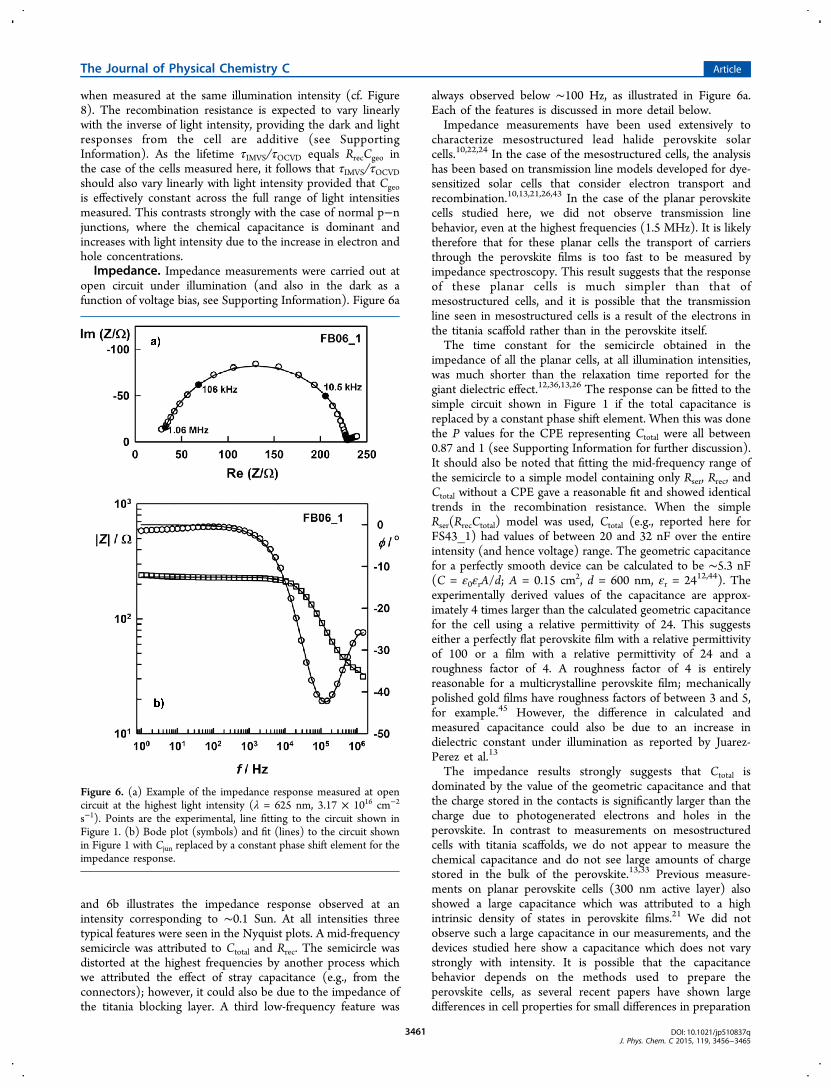
open circuit under illumination (and also in the dark as afunction of voltage bias, see Supporting Information). Figure 6a
and 6b illustrates the impedance response observed at anintensity corresponding to ∼0.1 Sun. At all intensities threetypical features were seen in the Nyquist plots. A mid-frequencysemicircle was attributed to Ctotal and Rrec. The semicircle wasdistorted at the highest frequencies by another process whichwe attributed the effect of stray capacitance (e.g., from theconnectors); however, it could also be due to the impedance ofthe titania blocking layer. A third low-frequency feature was
always observed below ∼100 Hz, as illustrated in Figure 6a.Each of the features is discussed in more detail below.Impedance measurements have been used extensively to
characterize mesostructured lead halide perovskite solarcells.10,22,24 In the case of the mesostructured cells, the analysishas been based on transmission line models developed for dye-sensitized solar cells that consider electron transport andrecombination.10,13,21,26,43 In the case of the planar perovskitecells studied here, we did not observe transmission linebehavior, even at the highest frequencies (1.5 MHz). It is likelytherefore that for these planar cells the transport of carriersthrough the perovskite films is too fast to be measured byimpedance spectroscopy. This result suggests that the responseof these planar cells is much simpler than that ofmesostructured cells, and it is possible that the transmissionline seen in mesostructured cells is a result of the electrons inthe titania scaffold rather than in the perovskite itself.The time constant for the semicircle obtained in the
impedance of all the planar cells, at all illumination intensities,was much shorter than the relaxation time reported for thegiant dielectric effect.12,36,13,26 The response can be fitted to thesimple circuit shown in Figure 1 if the total capacitance isreplaced by a constant phase shift element. When this was donethe P values for the CPE representing Ctotal were all between0.87 and 1 (see Supporting Information for further discussion).It should also be noted that fitting the mid-frequency range ofthe semicircle to a simple model containing only Rser, Rrec, andCtotal without a CPE gave a reasonable fit and showed identicaltrends in the recombination resistance. When the simpleRser(RrecCtotal) model was used, Ctotal (e.g., reported here forFS43_1) had values of between 20 and 32 nF over the entireintensity (and hence voltage) range. The geometric capacitancefor a perfectly smooth device can be calculated to be ∼5.3 nF(C = ε0εrA/d; A = 0.15 cm2, d = 600 nm, εr = 2412,44). Theexperimentally derived values of the capacitance are approx-imately 4 times larger than the calculated geometric capacitancefor the cell using a relative permittivity of 24. This suggestseither a perfectly flat perovskite film with a relative permittivityof 100 or a film with a relative permittivity of 24 and aroughness factor of 4. A roughness factor of 4 is entirelyreasonable for a multicrystalline perovskite film; mechanicallypolished gold films have roughness factors of between 3 and 5,for example.45 However, the difference in calculated andmeasured capacitance could also be due to an increase indielectric constant under illumination as reported by Juarez-Perez et al.13
The impedance results strongly suggests that Ctotal isdominated by the value of the geometric capacitance and thatthe charge stored in the contacts is significantly larger than thecharge due to photogenerated electrons and holes in theperovskite. In contrast to measurements on mesostructuredcells with titania scaffolds, we do not appear to measure thechemical capacitance and do not see large amounts of chargestored in the bulk of the perovskite.13,33 Previous measure-ments on planar perovskite cells (300 nm active layer) alsoshowed a large capacitance which was attributed to a highintrinsic density of states in perovskite films.21 We did notobserve such a large capacitance in our measurements, and thedevices studied here show a capacitance which does not varystrongly with intensity. It is possible that the capacitancebehavior depends on the methods used to prepare theperovskite cells, as several recent papers have shown largedifferences in cell properties for small differences in preparation
Figure 6. (a) Example of the impedance response measured at opencircuit at the highest light intensity (λ = 625 nm, 3.17 × 1016 cm−2
s−1). Points are the experimental, line fitting to the circuit shown inFigure 1. (b) Bode plot (symbols) and fit (lines) to the circuit shownin Figure 1 with Cjun replaced by a constant phase shift element for theimpedance response.
The Journal of Physical Chemistry C Article
DOI: 10.1021/jp510837qJ. Phys. Chem. C 2015, 119, 3456−3465
3461

techniques.46−48 The fact that Cg dominates Cμ over thefrequency range is consistent with a p−i−n device, althoughother authors have suggested that perovskite solar cells mayfunction as p−n devices.49
The parallel resistance that accompanies Cgeo is attributed tothe recombination resistance. The lifetimes calculated from theproduct of Cgeo and Rrec agree well with the values measured byIMVS and OCVD (Figure 4 and Figure S9, SupportingInformation). We therefore conclude that the perovskite can beconsidered as essentially intrinsic. This is consistent with thevery low doping density (∼109 cm−3) calculated from thetransition to first-order decay seen in Figure 4. The variations ofthe recombination resistance with Voc and with intensity areshown in Figures 7 and 8. The semilogarithmic plots of Rrec vs
Voc for the two types of cells have different slopes as shown inFigure 7, reflecting the different ideality factors of the cells. Theideality factors of 2.7 and 4.8 are very similar to those obtainedfrom the intensity dependence of the open-circuit voltage (cf.Figure 2). By contrast, the intensity dependence of Rrec isalmost identical for both types of cells, with a slope close to −1,mirroring the intensity dependence of τIMVS measured by IMVS(cf. Figure 5).The low-frequency feature that appears in the impedance
plots below 100 Hz has not been studied in detail, as we wereconcerned that the cells could degrade on the time scale of thevery slow low-frequency measurements. Juarez-Perez et al.attribute the low-frequency feature to the GDE in theperovskite.13 We are currently looking at the low-frequencyfeature in more detail, but the conclusion of this paper is that asimple circuit gives a good fit to all data above 100 Hz.
■ IMPSIMPS has been extensively used to investigate carrier transportin DSC. It has also been used to study recombination andinterfacial transfer of minority carriers in illuminated semi-
conductor electrodes.39,40,50 IMPS was recently used by Guillenet al. to study mesostructured perovskite cells; two timeconstants were observed in one quadrant of the complex planeplot. Figure 9 shows a representative IMPS plot for FS43_1 at
0.1 Sun equivalent illumination. The high-frequency semicircleis incomplete as the LED could not be modulated satisfactorilyat frequencies higher than 200 kHz. The IMPS response forDSC is usually a semicircle trending to a 45° line toward theorigin at high frequencies. The characteristic frequency of thesemicircle is related to the electron transport time, which rangesfrom milliseconds to seconds, depending on the illuminationintensity. By contrast, in the case of the planar perovskite solar
Figure 7. Recombination resistance for the two different types of cellsmeasured at open circuit under different illumination intensities.Slopes of the lines shown are 281 mV/decade for FS43-1 and 161mV/decade for FB-06, corresponding to m values of 4.8 and 2.7,respectively.
Figure 8. Intensity dependence of the recombination resistance for thetwo cells. The broken line corresponds to a linear dependence of Rrecon incident photon flux.
Figure 9. IMPS response for FS43_1 showing the RC time constant athigh frequency and a low-frequency semicircle which is related totransport and recombination.
The Journal of Physical Chemistry C Article
DOI: 10.1021/jp510837qJ. Phys. Chem. C 2015, 119, 3456−3465
3462
cells studied here, the high-frequency semicircle is dominatedby the time constant RserCgeo of the cell, and it is difficult todeconvolute the effect of carrier transport because the carriertransit times are similar to or shorter than the RC timeconstant. However, we believe that the distortion of thesemicircle at high frequencies may not be an instrumentalartifact but could be due to an additional phase lag associatedwith transport. The values of the series resistance measured byimpedance spectroscopy were used to estimate the capacitancefrom the relaxation time for the high-frequency semicircle. Theseries resistance for FB06_1, for example, was ∼40 Ω, whichgave capacitance values of between 26 and 36 nF. These valuesare consistent with the values of Ctotal obtained from bothIMVS and impedance spectroscopy.Interestingly, a second semicircle in the lower quadrant is
seen at lower frequencies. As discussed above, a similarresponse is observed for illuminated semiconductor/electrolytejunctions, where the second semicircle is due to the relaxationof the minority carrier concentration at short circuit by chargetransfer (with rate ktrans) and recombination (with rate krec) atthe solution−electrode interface. The high-frequency interceptcorresponds to the instantaneous photocurrent and the low-frequency limit to the steady-state photocurrent. In this case,the semicircle has a radial frequency at the minimum that isequal to the inverse of the relaxation lifetime, τIMPS
−1 = ktrans +krec, and a normalized low-frequency intercept that depends onthe charge transfer efficiency, ηtrans = ktrans/(ktrans + krec). Itshould be noted that the “relaxation lifetime” measured usingIMPS is quite separate from the “recombination lifetime”,which is measured at open circuit. The open-circuitrecombination lifetime is the product of the chemicalcapacitance and the recombination resistance. In contrast, therelaxation lifetime from IMPS is measured at short circuit. TheIMPS lifetime is not influenced by the geometric capacitancewhich, as outlined above, is observed in the high-frequencysemicircle in the upper quadrant of the IMPS plot. IMPS cantherefore give useful information about interfacial chargetransport and recombination in perovskite solar cells at shortcircuit.In view of the similarity mentioned above, we attribute the
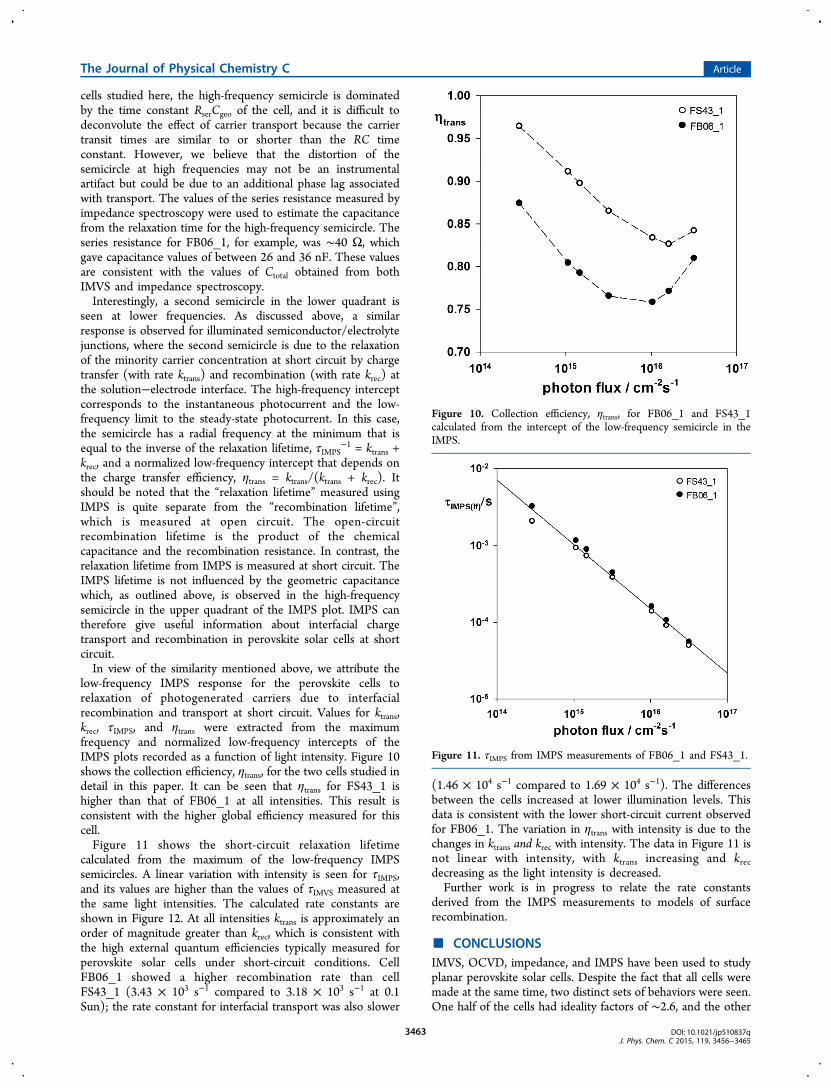
low-frequency IMPS response for the perovskite cells torelaxation of photogenerated carriers due to interfacialrecombination and transport at short circuit. Values for ktrans,krec, τIMPS, and ηtrans were extracted from the maximumfrequency and normalized low-frequency intercepts of theIMPS plots recorded as a function of light intensity. Figure 10shows the collection efficiency, ηtrans, for the two cells studied indetail in this paper. It can be seen that ηtrans for FS43_1 ishigher than that of FB06_1 at all intensities. This result isconsistent with the higher global efficiency measured for thiscell.Figure 11 shows the short-circuit relaxation lifetime
calculated from the maximum of the low-frequency IMPSsemicircles. A linear variation with intensity is seen for τIMPS,and its values are higher than the values of τIMVS measured atthe same light intensities. The calculated rate constants areshown in Figure 12. At all intensities ktrans is approximately anorder of magnitude greater than krec, which is consistent withthe high external quantum efficiencies typically measured forperovskite solar cells under short-circuit conditions. CellFB06_1 showed a higher recombination rate than cellFS43_1 (3.43 × 10³ s−1 compared to 3.18 × 10³ s−1 at 0.1Sun); the rate constant for interfacial transport was also slower
(1.46 × 10⁴ s−1 compared to 1.69 × 10⁴ s−1). The differencesbetween the cells increased at lower illumination levels. Thisdata is consistent with the lower short-circuit current observedfor FB06_1. The variation in ηtrans with intensity is due to thechanges in ktrans and krec with intensity. The data in Figure 11 isnot linear with intensity, with ktrans increasing and krecdecreasing as the light intensity is decreased.Further work is in progress to relate the rate constants
derived from the IMPS measurements to models of surfacerecombination.
■ CONCLUSIONSIMVS, OCVD, impedance, and IMPS have been used to studyplanar perovskite solar cells. Despite the fact that all cells weremade at the same time, two distinct sets of behaviors were seen.One half of the cells had ideality factors of ∼2.6, and the other
Figure 10. Collection efficiency, ηtrans, for FB06_1 and FS43_1calculated from the intercept of the low-frequency semicircle in theIMPS.
Figure 11. τIMPS from IMPS measurements of FB06_1 and FS43_1.
The Journal of Physical Chemistry C Article
DOI: 10.1021/jp510837qJ. Phys. Chem. C 2015, 119, 3456−3465
3463

half showed ideality factors of ∼5.2.The difference in behaviorwas also seen in the OCVD: the cells with the lower idealityfactors showed a persistent photovoltage. Lifetimes from IMVSwere in good agreement with those calculated from OCVD.IMVS and impedance spectroscopy showed time constants thatwere dominated by the geometric capacitance rather than thechemical capacitance, meaning that the ambipolar recombina-tion lifetime could not be extracted. IMPS showed twosemicircles, one at high frequency attributed to the RC timeconstant of the cells and a second at lower frequency attributedto interfacial transport and recombination at short circuit.Analysis of the IMPS response suggests that the collection ofphotogenerated carriers is very efficient under short-circuitconditions in these planar perovskite cells
■ ASSOCIATED CONTENT*S Supporting InformationIV characteristics and cell efficiencies, IMVS results, analysis ofconstant phase shift elements, dark impedance, OCVD fittingand theory, and modeling of the geometric and chemicalcapacitance for a planar p−i−n cell. This material is availablefree of charge via the Internet at http://pubs.acs.org.
■ AUTHOR INFORMATIONCorresponding Authors*E-mail: [email protected].*E-mail: [email protected] ContributionsThe manuscript was written through contributions of allauthors. All authors have given approval to the final version ofthe manuscript.NotesThe authors declare no competing financial interest.
■ ACKNOWLEDGMENTSThe authors thank Aron Walsh, Jarvist Frost, ChristopherEames, and Saiful Islam for helpful discussions. P.J.C. thanksthe EPSRC for funding (EP/G031088/1, EP/F047819/1, andDTC studentship for A.P., Grant EP/G03768X/1). Research
leading to these results has received funding from the EuropeanUnion Seventh Framework Programme [FP7/2007-2013]under grant agreement 316494.
■ REFERENCES(1) Liu, M.; Johnston, M. B.; Snaith, H. J. Efficient PlanarHeterojunction Perovskite Solar Cells by Vapour Deposition. Nature2013, 501, 395−398.(2) Lee, M. M.; Teuscher, J.; Miyasaka, T.; Murakami, T. N.; Snaith,H. J. Efficient Hybrid Solar Cells Based on Meso-SuperstructuredOrganometal Halide Perovskites. Science 2012, 338, 643−647.(3) Etgar, L.; Gao, P.; Xue, Z.; Peng, Q.; Chandiran, A. K.; Liu, B.;Nazeeruddin, M. K.; Gratzel, M. Mesoscopic CH3NH3PbI3/TiO2
Heterojunction Solar Cells. J. Am. Chem. Soc. 2012, 134, 17396−17399.(4) Kim, H.-S.; Lee, C.-R.; Im, J.-H.; Lee, K.-B.; Moehl, T.;Marchioro, A.; Moon, S.-J.; Humphry-Baker, R.; Yum, J.-H.; Moser, J.E.; et al. Lead Iodide Perovskite Sensitized All-Solid-State SubmicronThin Film Mesoscopic Solar Cell with Efficiency Exceeding 9%. Sci.Rep. 2012, 2, 591.(5) Bretschneider, S. A.; Weickert, J.; Dorman, J. A.; Schmidt-Mende,L. Research Update: Physical and Electrical Characteristics of LeadHalide Perovskites for Solar Cell Applications. APL Mater. 2014, 2,040701.(6) Ryu, S.; Noh, J. H.; Jeon, N. J.; Kim, Y. C.; Yang, W. S.; Seo, J.W.; Seok, S. I. Voltage Output of Efficient Perovskite Solar Cells withHigh Open-Circuit Voltage and Fill Factor. Energy Environ. Sci. 2014,7, 2614−2618.(7) Wehrenfennig, C.; Eperon, G. E.; Johnston, M. B.; Snaith, H. J.;Herz, L. M. High Charge Carrier Mobilities and Lifetimes inOrganolead Trihalide Perovskites. Adv. Mater. 2014, 26, 1584−1589.(8) Yin, W.-J.; Shi, T.; Yan, Y. Unique Properties of HalidePerovskites as Possible Origins of the Superior Solar Cell Performance.Adv. Mater. 2014, 26, 4653−4658.(9) Ponseca, C. S.; Savenije, T. J.; Abdellah, M. A.; Zheng, K.;Yartsev, A. P.; Pascher, T.; Harlang, T.; Chabera, P.; Pullerits, T.;Stepanov, A.; et al. Organometal Halide Perovskite Solar CellMaterials Rationalized−Ultrafast Charge Generation, High andMicrosecond-Long Balanced Mobilities and Slow Recombination. J.Am. Chem. Soc. 2014, 136, 5189−5192.(10) Gonzalez-Pedro, V.; Juarez-Perez, E. J.; Arsyad, W.-S.; Barea, E.M.; Fabregat-Santiago, F.; Mora-Sero, I.; Bisquert, J. General WorkingPrinciples of CH3NH3PbX3 Perovskite Solar Cells. Nano Lett. 2014,14, 888−893.(11) Frost, J. M.; Butler, K. T.; Brivio, F.; Hendon, C. H.; vanSchilfgaarde, M.; Walsh, A. Atomistic Origins of High-Performance inHybrid Halide Perovskite Solar Cells. Nano Lett. 2014, 14, 2584−2590.(12) Frost, J. M.; Butler, K. T.; Walsh, A. Molecular FerroelectricContributions to Anomalous Hysteresis in Hybrid Perovskite SolarCells. APL Mater. 2014, 2, 081506.(13) Juarez-Perez, E. J.; Sanchez, R. S.; Badia, L.; Garcia-Belmonte,G.; Kang, Y. S.; Mora-Sero, I.; Bisquert, J. Photoinduced GiantDielectric Constant in Lead Halide Perovskite Solar Cells. J. Phys.Chem. Lett. 2014, 9, 2390−2394.(14) Zhou, H.; Chen, Q.; Li, G.; Luo, S.; Song, T.-b.; Duan, H.-S.;Hong, Z.; You, J.; Liu, Y.; Yang, Y. Interface Engineering of HighlyEfficient Perovskite Solar Cells. Science 2014, 345, 542−546.(15) Savenije, T. J.; Ponseca, C. S.; Kunneman, L. T.; Abdellah, M.A.; Zheng, K.; Tian, Y.; Zhu, Q.; Canton, S. E.; Scheblykin, I. G.;Pullerits, T.; et al. Thermally Activated Exciton Dissociation andRecombination Control the Organometal Halide Perovskite CarrierDynamics. J. Phys. Chem. Lett. 2014, 5, 2189−2194.(16) Marchioro, A.; Teuscher, J.; Friedrich, D.; Kunst, M.; van deKrol, R.; Moehl, T.; Gratzel, M.; Moser, J.-E. Unravelling theMechanism of Photoinduced Charge Transfer Processes in LeadIodide Perovskite Solar Cells. Nat. Photonics 2014, 8, 1−6.
Figure 12. Recombination rate constant (open symbols) and transportrate constant (solid symbols) as a function of intensity. Circles showdata for FB06_1, and triangles show data for FS43_1.
The Journal of Physical Chemistry C Article
DOI: 10.1021/jp510837qJ. Phys. Chem. C 2015, 119, 3456−3465
3464

(17) Wehrenfennig, C.; Liu, M.; Snaith, H. J.; Johnston, M. B.; Herz,I. Charge-Carrier Dynamics in Vapour-Deposited Films of theOrganolead Halide Perovskite CH3NH3PbI3−xClx. Energy Environ.Sci. 2014, 2269−2275.(18) Stranks, S. D.; Eperon, G. E.; Grancini, G.; Menelaou, C.;Alcocer, M. J. P.; Leijtens, T.; Herz, L. M.; Petrozza, A.; Snaith, H. J.Electron-Hole Diffusion Lengths Exceeding 1 Micrometer in anOrganometal Trihalide Perovskite Absorber. Science 2013, 342, 341−344.(19) Edri, E.; Kirmayer, S.; Henning, A.; Mukhopadhyay, S.;Gartsman, K.; Rosenwaks, Y.; Hodes, G.; Cahen, D. Why LeadMethylammonium Tri-Iodide Perovskite-Based Solar Cells Require aMesoporous Electron Transporting Scaffold (but Not Necessarily aHole Conductor). Nano Lett. 2014, 14, 1000−1004.(20) Abate, A.; Saliba, M.; Hollman, D. J.; Stranks, S. D.;Wojciechowski, K.; Avolio, R.; Grancini, G.; Petrozza, A.; Snaith, H.J. Supramolecular Halogen Bond Passivation of Organic-InorganicHalide Perovskite Solar Cells. Nano Lett. 2014, 3247−3254.(21) Kim, H.-S.; Mora-Sero, I.; Gonzalez-Pedro, V.; Fabregat-Santiago, F.; Juarez-Perez, E. J.; Park, N.-G.; Bisquert, J. Mechanism ofCarrier Accumulation in Perovskite Thin-Absorber Solar Cells. Nat.Commun. 2013, 4, 2242.(22) Dualeh, A.; Moehl, T.; Tetreault, N.; Teuscher, J.; Gao, P.;Nazeeruddin, M. K.; Gratzel, M. Impedance Spectroscopic Analysis ofLead Iodide Perovskite-Sensitized Solid-State Solar Cells. ACS Nano2014, 8, 362−373.(23) Sanchez, R. S.; Gonzalez-Pedro, V.; Lee, J.-W.; Park, N.-G.;Kang, Y. S.; Mora-Sero, I.; Bisquert, J. Slow Dynamic Processes inLead Halide Perovskite Solar Cells. Characteristic Times andHysteresis. J. Phys. Chem. Lett. 2014, 5, 2357−2363.(24) Suarez, B.; Gonzalez-Pedro, V.; Ripolles, T. S.; Sanchez, R. S.;Otero, L. A.; Mora-Sero, I. Recombination Study of Combined Halides(Cl, Br, I) Perovskite Solar Cells. J. Phys. Chem. Lett. 2014, 5, 1628−1635.(25) Baumann, A.; Tvingstedt, K.; Heiber, M. C.; Vath, S.;Momblona, C.; Bolink, H. J.; Dyakonov, V. Persistent Photovoltagein Methylammonium Lead Iodide Perovskite Solar Cells. APL Mater.2014, 2, 081501.(26) Bisquert, J.; Bertoluzzi, L.; Mora-Sero, I.; Garcia-Belmonte, G.Theory of Impedance and Capacitance Spectroscopy of Solar Cellswith Dielectric Relaxation, Drift-Diffusion Transport, and Recombi-nation. J. Phys. Chem. C 2014, 118, 18983−18991.(27) Landsberg, P. T. Recombination in Semiconductors; CambridgeUniversity Press: Cambridge, U.K., 1991.(28) Shah, J. M.; Li, Y.-L.; Gessmann, T.; Schubert, E. F.Experimental Analysis and Theoretical Model for Anomalously HighIdeality Factors (N≫2.0) in AlGaN/GaN P-N Junction Diodes. J.Appl. Phys. 2003, 94, 2627−2630.(29) Brug, G. J.; van den Eeden, A. L. G.; Sluyters-Rehbach, M.;Sluyters, J. H. The Analysis of Electrode Impedances Complicated bythe Presence of a Constant Phase Element. J. Electroanal. Chem.Interfacial 1984, 176, 275−295.(30) Hirschorn, B.; Orazem, M. E.; Tribollet, B.; Vivier, V.; Frateur,I.; Musiani, M. Constant-Phase-Element Behavior Caused byResistivity Distributions in Films. In Corrosion; Hansen, D. C.,Alfantazi, A., Gelling, V. J., Eds.; The Electrochemical Society: NewJersey, 2010; Vol. 28, pp 77−94.(31) Mora-Sero, I.; Garcia-Belmonte, G.; Boix, P. P.; Vazquez, M. A.;Bisquert, J. Impedance Spectroscopy Characterisation of HighlyEfficient Silicon Solar Cells under Different Light IlluminationIntensities. Energy Environ. Sci. 2009, 2, 678−686.(32) Bisquert, J. Theory of the Impedance of Electron Diffusion andRecombination in a Thin Layer. J. Phys. Chem. B 2001, 106, 325−333.(33) Guillen, E.; Ramos, F. J.; Anta, J. A.; Ahmad, S. ElucidatingTransport-Recombination Mechanisms in Perovskite Solar Cells bySmall-Perturbation Techniques. J. Phys. Chem. C 2014, 118, 22913−22922.(34) Zhao, Y.; Nardes, A. M.; Zhu, K. Mesoporous Perovskite SolarCells: Material Composition, Charge-Carrier Dynamics, and Device
Characteristics. Faraday Discuss. 2014, Advance article. http://dx.doi.org/10.1039/C4FD00128A.(35) Zhao, Y.; Nardes, A. M.; Zhu, K. Solid-State MesostructuredPerovskite CH3NH3PbI3 Solar Cells: Charge Transport, Recombina-tion, and Diffusion Length. J. Phys. Chem. Lett. 2014, 5, 490−494.(36) Zaban, A.; Greenshtein, M.; Bisquert, J. Determination of theElectron Lifetime in Nanocrystalline Dye Solar Cells by Open-CircuitVoltage Decay Measurements. ChemPhysChem 2003, 4, 859−864.(37) Franco, G.; Peter, L. M.; Ponomarev, E. A. Detection ofInhomogeneous Dye Distribution in Dye Sensitised NanocrystallineSolar Cells by Intensity Modulated Photocurrent Spectroscopy(IMPS). Electrochem. Commun. 1999, 1, 61−64.(38) Ponomarev, E. A.; Peter, L. M. A Generalized Theory ofIntensity Modulated Photocurrent Spectroscopy (IMPS). J. Electroa-nal. Chem. 1995, 396, 219−226.(39) Peter, L. M.; Ponomarev, E. A.; Fermín, D. J. Intensity-Modulated Photocurrent Spectroscopy: Reconciliation of Phenom-enological Analysis with Multistep Electron Transfer Mechanisms. J.Electroanal. Chem. 1997, 427, 79−96.(40) Peter, L. M.; Wijayantha, K. G. U.; Tahir, A. A. Kinetics ofLight-Driven Oxygen Evolution at alpha-Fe2O3 Electrodes. FaradayDiscuss. 2012, 155, 309−322.(41) Grancini, G.; Marras, S.; Prato, M.; Giannini, C.; Quarti, C.; DeAngelis, F.; De Bastiani, M.; Eperon, G. E.; Snaith, H. J.; Manna, L.;et al. The Impact of the Crystallization Processes on the Structural andOptical Properties of Hybrid Perovskite Films for Photovoltaics. J.Phys. Chem. Lett. 2014, 5, 3836−3842.(42) Gottesman, R.; Haltzi, E.; Gouda, L.; Tirosh, S.; Bouhadana, Y.;Zaban, A.; Mosconi, E.; De Angelis, F. Extremely Slow Photo-conductivity Response of CH3NH3PbI3 Perovskites SuggestingStructural Changes under Working Conditions. J. Phys. Chem. Lett.2014, 5, 2662−2669.(43) Bertoluzzi, L.; Boix, P. P.; Mora-Sero, I.; Bisquert, J. Theory ofImpedance Spectroscopy of Ambipolar Solar Cells with Trap-Mediated Recombination. J. Phys. Chem. C 2013, 118, 16574−16580.(44) Brivio, F.; Walker, A. B.; Walsh, A. Structural and ElectronicProperties of Hybrid Perovskites for High-Efficiency Thin-FilmPhotovoltaics from First-Principles. APL Mater. 2013, 1, 042111.(45) Douglass, E. F., Jr; Driscoll, P. F.; Liu, D.; Burnham, N. A.;Lambert, C. R.; McGimpsey, W. G. Effect of Electrode Roughness onthe Capacitive Behavior of Self-Assembled Monolayers. Anal. Chem.2008, 80, 7670−7677.(46) Im, J.-H.; Kim, H.-S.; Park, N.-G. Morphology-PhotovoltaicProperty Correlation in Perovskite Solar Cells: One-Step Versus Two-Step Deposition of CH3NH3PbI3. APL Mater. 2014, 2, 081510.(47) Bass, K. K.; McAnally, R. E.; Zhou, S.; Djurovich, P. I.;Thompson, M. E.; Melot, B. C. Influence of Moisture on thePreparation, Crystal Structure, and Photophysical Properties ofOrganohalide Perovskites. Chem. Commun. 2014, 50, 15819−15822.(48) Buin, A.; Pietsch, P.; Xu, J.; Voznyy, O.; Ip, A. H.; Comin, R.;Sargent, E. H. Materials Processing Routes to Trap-Free HalidePerovskites. Nano Lett. 2014, 14, 6281−6286.(49) Guerrero, A.; Juarez-Perez, E. J.; Bisquert, J.; Mora-Sero, I.;Garcia-Belmonte, G. Electrical Field Profile and Doping in Planar LeadHalide Perovskite Solar Cells. Appl. Phys. Lett. 2014, 105, 133902.(50) Peter, L. M. Dynamic Aspects of Semiconductor Photo-electrochemistry. Chem. Rev. 1990, 90, 753−769.
The Journal of Physical Chemistry C Article
DOI: 10.1021/jp510837qJ. Phys. Chem. C 2015, 119, 3456−3465
3465


![Highly efficient and stable planar perovskite solar …ppl/2004ppl/2015_03_[Nano energy]_JSYeo.pdfHighly efficient and stable planar perovskite solar cells with reduced graphene oxide](https://static.fdocuments.us/doc/165x107/5add39787f8b9a9d4d8cd866/highly-efficient-and-stable-planar-perovskite-solar-ppl2004ppl201503nano.jpg)