Advanced USB transceiversdatasheet.elcodis.com/pdf2/69/86/698698/isp1105wts.pdf · They allow USB...
25
1. General description The ISP1105/1106 range of Universal Serial Bus (USB) transceivers are compliant with the Universal Serial Bus Specification Rev. 2.0. They can transmit and receive serial data at both full-speed (12 Mbit/s) and low-speed (1.5 Mbit/s) data rates. The ISP1105/1106 range can be used as a USB device transceiver or a USB host transceiver. They allow USB Application Specific ICs (ASICs) and Programmable Logic Devices (PLDs) with power supply voltages from 1.65 V to 3.6 V to interface with the physical layer of the Universal Serial Bus. They have an integrated 5 V-to-3.3 V voltage regulator for direct powering via the USB supply V BUS . ISP1105 allows single-ended and differential input modes selectable by a MODE input and it is available in HVQFN16 and HBCC16 packages. ISP1106 allows only differential input mode and is available in both TSSOP16 and HBCC16 packages. The ISP1105/1106 are ideal for portable electronics devices such as mobile phones, digital still cameras, Personal Digital Assistants (PDA) and Information Appliances (IA). 2. Features Complies with Universal Serial Bus Specification Rev. 2.0 Can transmit and receive serial data at both full-speed (12 Mbit/s) and low-speed (1.5 Mbit/s) data rates Integrated bypassable 5 V-to-3.3 V voltage regulator for powering via USB V BUS V BUS disconnection indication through VP and VM Used as a USB device transceiver or a USB host transceiver Stable RCV output during SE0 condition Two single-ended receivers with hysteresis Low-power operation Supports an I/O voltage range from 1.65 V to 3.6 V ±12 kV ESD protection at the D+, D−, V CC(5.0) and GND pins Full industrial operating temperature range from −40 °C to +85 °C Available in small HBCC16, HVQFN16 (only ISP1105) and TSSOP16 (only ISP1106) packages The ISP1105 HBCC16 and HVQFN16 are lead-free and halogen-free. The ISP1106 HBCC16 is lead-free. ISP1105/1106 Advanced USB transceivers Rev. 10 — 28 September 2009 Product data sheet
Transcript of Advanced USB transceiversdatasheet.elcodis.com/pdf2/69/86/698698/isp1105wts.pdf · They allow USB...

1. General description
The ISP1105/1106 range of Universal Serial Bus (USB) transceivers are compliant with the Universal Serial Bus Specification Rev. 2.0. They can transmit and receive serial data at both full-speed (12 Mbit/s) and low-speed (1.5 Mbit/s) data rates. The ISP1105/1106 range can be used as a USB device transceiver or a USB host transceiver.
They allow USB Application Specific ICs (ASICs) and Programmable Logic Devices (PLDs) with power supply voltages from 1.65 V to 3.6 V to interface with the physical layer of the Universal Serial Bus. They have an integrated 5 V-to-3.3 V voltage regulator for direct powering via the USB supply VBUS.
ISP1105 allows single-ended and differential input modes selectable by a MODE input and it is available in HVQFN16 and HBCC16 packages. ISP1106 allows only differential input mode and is available in both TSSOP16 and HBCC16 packages.
The ISP1105/1106 are ideal for portable electronics devices such as mobile phones, digital still cameras, Personal Digital Assistants (PDA) and Information Appliances (IA).
2. Features
Complies with Universal Serial Bus Specification Rev. 2.0Can transmit and receive serial data at both full-speed (12 Mbit/s) and low-speed (1.5 Mbit/s) data ratesIntegrated bypassable 5 V-to-3.3 V voltage regulator for powering via USB VBUS
VBUS disconnection indication through VP and VMUsed as a USB device transceiver or a USB host transceiverStable RCV output during SE0 conditionTwo single-ended receivers with hysteresisLow-power operationSupports an I/O voltage range from 1.65 V to 3.6 V±12 kV ESD protection at the D+, D−, VCC(5.0) and GND pinsFull industrial operating temperature range from −40 °C to +85 °CAvailable in small HBCC16, HVQFN16 (only ISP1105) and TSSOP16 (only ISP1106) packagesThe ISP1105 HBCC16 and HVQFN16 are lead-free and halogen-free.The ISP1106 HBCC16 is lead-free.
ISP1105/1106Advanced USB transceiversRev. 10 — 28 September 2009 Product data sheet

ISP1105/1106Advanced USB transceivers
3. Applications
Portable electronic devices, such as:Mobile phoneDigital still cameraPersonal Digital Assistant (PDA)Information Appliance (IA).
4. Ordering information
4.1 Ordering options
Table 1. Ordering informationCommercial product code
Package description Packing Minimum sellable quantity
ISP1105BSTM HVQFN16; 16 terminals; body 3 × 3 × 0.85 mm 13 inch tape and reel non-dry pack 6000 pieces
ISP1105WTS HBCC16; 16 terminals; body 3 × 3 × 0.65 mm 7 inch tape and reel non-dry pack 1400 pieces
ISP1105WTM HBCC16; 16 terminals; body 3 × 3 × 0.65 mm 13 inch tape and reel non-dry pack 6000 pieces
ISP1106WTS HBCC16; 16 terminals; body 3 × 3 × 0.65 mm 7 inch tape and reel non-dry pack 1400 pieces
ISP1106DHTM TSSOP16; 16 leads; body width 4.4 mm 13 inch tape and reel non-dry pack 2500 pieces
Table 2. Selection guideProduct Package DescriptionISP1105 HVQFN16 and HBCC16 supports both single-ended and differential input modes; see Table 5 and
Table 6.
ISP1106 TSSOP16 and HBCC16 supports only the differential input mode; see Table 6.
ISP1105_1106_10 © ST-ERICSSON 2009. All rights reserved.
Product data sheet Rev. 10 — 28 September 2009 2 of 25

ISP1105/1106Advanced USB transceivers
5. Block diagram
(1) Connect to D− for low-speed operation.(2) Pin function depends on device type.(3) Only for ISP1105.
Fig 1. Block diagram (combined ISP1105 and ISP1106).
mbl301
VCC(I/O) VCC(5.0)VOLTAGE
REGULATOR
3.3 V
1.5 kΩ(1)
33 Ω (1%)
33 Ω (1%)
LEVELSHIFTER
ISP1105ISP1106
SOFTCON
SPEED
Vreg(3.3)
GND
Vpu(3.3)
D+
D−
OE
VMO/FSE0(2)
VPO/VO(2)
MODE(3)
SUSPND
RCV
VP
VM
ISP1105_1106_10 © ST-ERICSSON 2009. All rights reserved.
Product data sheet Rev. 10 — 28 September 2009 3 of 25

ISP1105/1106Advanced USB transceivers
6. Pinning information
6.1 Pinning
Fig 2. Pin configuration ISP1105BSTM (HVQFN). Fig 3. Pin configuration ISP1105WTS and ISP1105WTM (HBCC16).
004aaa314
ISP1105BSTM
D−
D+
MO
DE
SU
SP
ND
VPO/VO
VMO/FSE0
8
GND(exposed diepad)
VC
C(I
/O)
5 6 7
4
3
2
9
10
11
13141516
SP
EE
D
1 12
Bottom view
RCV
VP
OE
VM
Vpu
(3.3
)
SO
FT
CO
N
VC
C(5
.0)
Vre
g(3.
3)
MBL303Bottom view
ISP1105WTSISP1105WTM
SO
FT
CO
N
Vpu
(3.3
)
RCV
VP
OE
D+
D−
SP
EE
D
VC
C(I
/O)
VPO/VO
VM
SUSPND
MO
DE
VC
C(5
.0)
Vreg(3.3)
VMO/FSE0
13141516
876
12
11
10
9
2
1
3
4
5
GND(exposed diepad)
Fig 4. Pin configuration ISP1106DHTM (TSSOP16). Fig 5. Pin configuration ISP1106WTS (HBCC16).
ISP1106DHTM
MBL302
1
2
3
4
5
6
7
8
16
15
14
13
12
11
10
9
Vpu(3.3)
SOFTCON
OE
RCV
VP
VM
SUSPND
GND VCC(I/O)
SPEED
D−
D+
VPO
VMO
Vreg(3.3)
VCC(5.0)
MBL304Bottom view
ISP1106WTS
SO
FT
CO
N
Vpu
(3.3
)
RCV
VP
OE
D+
D−
SP
EE
D
VC
C(I
/O)
VPO
VM
SUSPND
GN
D
VC
C(5
.0)
Vreg(3.3)
VMO
13141516
876
12
11
10
9
2
1
3
4
5
ISP1105_1106_10 © ST-ERICSSON 2009. All rights reserved.
Product data sheet Rev. 10 — 28 September 2009 4 of 25
ISP1105/1106Advanced USB transceivers
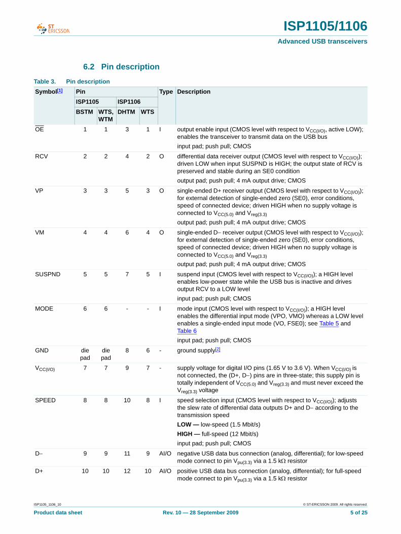
6.2 Pin description
Table 3. Pin descriptionSymbol[1] Pin Type Description
ISP1105 ISP1106BSTM WTS,
WTMDHTM WTS
OE 1 1 3 1 I output enable input (CMOS level with respect to VCC(I/O), active LOW); enables the transceiver to transmit data on the USB businput pad; push pull; CMOS
RCV 2 2 4 2 O differential data receiver output (CMOS level with respect to VCC(I/O)); driven LOW when input SUSPND is HIGH; the output state of RCV is preserved and stable during an SE0 conditionoutput pad; push pull; 4 mA output drive; CMOS
VP 3 3 5 3 O single-ended D+ receiver output (CMOS level with respect to VCC(I/O)); for external detection of single-ended zero (SE0), error conditions, speed of connected device; driven HIGH when no supply voltage is connected to VCC(5.0) and Vreg(3.3)
output pad; push pull; 4 mA output drive; CMOS
VM 4 4 6 4 O single-ended D− receiver output (CMOS level with respect to VCC(I/O)); for external detection of single-ended zero (SE0), error conditions, speed of connected device; driven HIGH when no supply voltage is connected to VCC(5.0) and Vreg(3.3)
output pad; push pull; 4 mA output drive; CMOS
SUSPND 5 5 7 5 I suspend input (CMOS level with respect to VCC(I/O)); a HIGH level enables low-power state while the USB bus is inactive and drives output RCV to a LOW levelinput pad; push pull; CMOS
MODE 6 6 - - I mode input (CMOS level with respect to VCC(I/O)); a HIGH level enables the differential input mode (VPO, VMO) whereas a LOW level enables a single-ended input mode (VO, FSE0); see Table 5 and Table 6 input pad; push pull; CMOS
GND die pad
die pad
8 6 - ground supply[2]
VCC(I/O) 7 7 9 7 - supply voltage for digital I/O pins (1.65 V to 3.6 V). When VCC(I/O) is not connected, the (D+, D−) pins are in three-state; this supply pin is totally independent of VCC(5.0) and Vreg(3.3) and must never exceed the Vreg(3.3) voltage
SPEED 8 8 10 8 I speed selection input (CMOS level with respect to VCC(I/O)); adjusts the slew rate of differential data outputs D+ and D− according to the transmission speedLOW — low-speed (1.5 Mbit/s)HIGH — full-speed (12 Mbit/s)input pad; push pull; CMOS
D− 9 9 11 9 AI/O negative USB data bus connection (analog, differential); for low-speed mode connect to pin Vpu(3.3) via a 1.5 kΩ resistor
D+ 10 10 12 10 AI/O positive USB data bus connection (analog, differential); for full-speed mode connect to pin Vpu(3.3) via a 1.5 kΩ resistor
ISP1105_1106_10 © ST-ERICSSON 2009. All rights reserved.
Product data sheet Rev. 10 — 28 September 2009 5 of 25

ISP1105/1106Advanced USB transceivers
[1] Symbol names with an overscore (e.g. NAME) indicate active LOW signals.
[2] ISP1105: ground terminal is connected to the exposed die pad (heat sink).
VPO/VO 11 11 - - I driver data input (CMOS level with respect to VCC(I/O), Schmitt trigger); see Table 5 and Table 6input pad; push pull; CMOS
VPO - - 13 11
VO - - - -
VMO/FSE0 12 12 - - I driver data input (CMOS level with respect to VCC(I/O), Schmitt trigger); see Table 5 and Table 6input pad; push pull; CMOS
VMO - - 14 12
FSE0 - - - -
Vreg(3.3) 13 13 15 13 - internal regulator option: regulated supply voltage output (3.0 V to 3.6 V) during 5 V operation; a decoupling capacitor of at least 0.1 μF is requiredregulator bypass option: used as a supply voltage input for 3.3 V ± 10 % operation
VCC(5.0) 14 14 16 14 - internal regulator option: supply voltage input (4.0 V to 5.5 V); can be connected directly to USB supply VBUS
regulator bypass option: connect to Vreg(3.3)
Vpu(3.3) 15 15 1 15 - pull-up supply voltage (3.3 V ± 10 %); connect an external 1.5 kΩ resistor on D+ (full-speed) or D− (low-speed); pin function is controlled by input SOFTCONSOFTCON = LOW — Vpu(3.3) floating (high impedance); ensures zero pull-up currentSOFTCON = HIGH — Vpu(3.3) = 3.3 V; internally connected to Vreg(3.3)
SOFTCON 16 16 2 16 I software controlled USB connection input; a HIGH level applies 3.3 V to pin Vpu(3.3), which is connected to an external 1.5 kΩ pull-up resistor; this allows USB connect/disconnect signalling to be controlled by softwareinput pad; push pull; CMOS
Table 3. Pin description …continued
Symbol[1] Pin Type DescriptionISP1105 ISP1106BSTM WTS,
WTMDHTM WTS
ISP1105_1106_10 © ST-ERICSSON 2009. All rights reserved.
Product data sheet Rev. 10 — 28 September 2009 6 of 25

ISP1105/1106Advanced USB transceivers
7. Functional description
7.1 Function selection
[1] Signal levels on (D+, D−) are determined by other USB devices and external pull-up/down resistors.
[2] In ‘suspend’ mode (SUSPND = HIGH) the differential receiver is inactive and output RCV is always LOW. Out-of-suspend (‘K’) signalling is detected via the single-ended receivers VP and VM.
[3] During suspend, the slew-rate control circuit of low-speed operation is disabled. The (D+, D−) lines are still driven to their intended states, without slew-rate control. This is permitted because driving during suspend is used to signal remote wake-up by driving a ‘K’ signal (one transition from idle to ‘K’ state) for a period of 1 to 15 ms.
7.2 Operating functions
[1] VP = VM = H indicates the sharing mode (VCC(5.0) and Vreg(3.3) are disconnected).
[2] RCV* denotes the signal level on output RCV just before SE0 state occurs. This level is stable during the SE0 period.
Table 4. Function tableSUSPND OE (D+, D−) RCV VP/VM FunctionL L driving and
receivingactive active normal driving (differential
receiver active)
L H receiving[1] active active receiving
H L driving inactive[2] active driving during ‘suspend’[3] (differential receiver inactive)
H H high-Z[1] inactive[2] active low-power state
Table 5. Driving function (pin OE = L) using single-ended input data interface for ISP1105 (pin MODE = L)
FSE0 VO DataL L differential logic 0
L H differential logic 1
H L SE0
H H SE0
Table 6. Driving function (pin OE = L) using differential input data interface for ISP1105 (pin MODE = H) and ISP1106
VMO VPO DataL L SE0
L H differential logic 1
H L differential logic 0
H H illegal state
Table 7. Receiving function (pin OE = H)(D+, D−) RCV VP[1] VM[1]
Differential logic 0 L L H
Differential logic 1 H H L
SE0 RCV*[2] L L
ISP1105_1106_10 © ST-ERICSSON 2009. All rights reserved.
Product data sheet Rev. 10 — 28 September 2009 7 of 25

ISP1105/1106Advanced USB transceivers
7.3 Power supply configurationsThe ISP1105/1106 can be used with different power supply configurations, which can be changed dynamically. An overview is given in Table 9.
Normal mode — Both VCC(I/O) and VCC(5.0) or (VCC(5.0) and Vreg(3.3)) are connected. For 5 V operation, VCC(5.0) is connected to a 5 V source (4.0 V to 5.5 V). The internal voltage regulator then produces 3.3 V for the USB connections. For 3.3 V operation, both VCC(5.0) and Vreg(3.3) are connected to a 3.3 V source (3.0 V to 3.6 V). VCC(I/O) is independently connected to a voltage source (1.65 V to 3.6 V), depending on the supply voltage of the external circuit. Disable mode — VCC(I/O) is not connected, VCC(5.0) or (VCC(5.0) and Vreg(3.3)) are connected. In this mode, the internal circuits of the ISP1105/1106 ensure that the (D+, D−) pins are in three-state and the power consumption drops to the low-power (suspended) state level. Some hysteresis is built into the detection of VCC(I/O) lost.Sharing mode — VCC(I/O) is connected, (VCC(5.0) and Vreg(3.3)) are not connected. In this mode, the (D+, D−) pins are made three-state and the ISP1105/1106 allows external signals of up to 3.6 V to share the (D+, D−) lines. The internal circuits of the ISP1105/1106 ensure that virtually no current (maximum 10 μA) is drawn via the (D+, D−) lines. The power consumption through pin VCC(I/O) drops to the low-power (suspended) state level. Both the VP and VM pins are driven HIGH to indicate this mode. Pin RCV is made LOW. Some hysteresis is built into the detection of Vreg(3.3) lost.
[1] High impedance or driven LOW.
[2] ISP1105 only.
[1] High impedance or driven LOW.
Table 8. Pin states in disable or sharing modePins Disable mode state Sharing mode stateVCC(5.0) / Vreg(3.3) 5 V input / 3.3 V output;
3.3 V input / 3.3 V inputnot present
VCC(I/O) not present 1.65 V to 3.6 V input
Vpu(3.3) high impedance (off) high impedance (off)
(D+, D−) high impedance high impedance
(VP, VM) invalid[1] H
RCV invalid[1] L
Inputs (VO/VPO, FSE0/VMO, SPEED, MODE[2], SUSPND, OE, SOFTCON)
high impedance high impedance
Table 9. Power supply configuration overviewVCC(5.0) or Vreg(3.3) VCC(I/O) Configuration Special characteristicsConnected connected normal mode -
Connected not connected disable mode (D+, D−) and Vpu(3.3) high impedance; VP, VM, RCV: invalid[1]
Not connected connected sharing mode (D+, D−) and Vpu(3.3) high impedance;VP, VM driven HIGH; RCV driven LOW
ISP1105_1106_10 © ST-ERICSSON 2009. All rights reserved.
Product data sheet Rev. 10 — 28 September 2009 8 of 25

ISP1105/1106Advanced USB transceivers
7.4 Power supply input optionsThe ISP1105/1106 range has two power supply input options.
Internal regulator — VCC(5.0) is connected to 4.0 V to 5.5 V. The internal regulator is used to supply the internal circuitry with 3.3 V (nominal). The Vreg(3.3) pin becomes a 3.3 V output reference.Regulator bypass — VCC(5.0) and Vreg(3.3) are connected to the same supply. The internal regulator is bypassed and the internal circuitry is supplied directly from the Vreg(3.3) power supply. The voltage range is 3.0 V to 3.6 V to comply with the USB specification.
The supply voltage range for each input option is specified in Table 10.
Table 10. Power supply input optionsInput option VCC(5.0) Vreg(3.3) VCC(I/O)
Internal regulator supply input for internal regulator (4.0 V to 5.5 V)
voltage reference output (3.3 V, 300 μA)
supply input for digital I/O pins (1.65 V to 3.6 V)
Regulator bypass connected to Vreg(3.3) with maximum voltage drop of 0.3 V (2.7 V to 3.6 V)
supply input (3.0 V to 3.6 V)
supply input for digital I/O pins (1.65 V to 3.6 V)
ISP1105_1106_10 © ST-ERICSSON 2009. All rights reserved.
Product data sheet Rev. 10 — 28 September 2009 9 of 25

ISP1105/1106Advanced USB transceivers
8. Electrostatic discharge (ESD)
8.1 ESD protectionThe pins that are connected to the USB connector (D+, D−, VCC(5.0) and GND) have a minimum of ±12 kV ESD protection. The ±12 kV measurement is limited by the test equipment. Capacitors of 4.7 μF connected from Vreg(3.3) to GND and VCC(5.0) to GND are required to achieve this ±12 kV ESD protection (see Figure 6).
8.2 ESD test conditionsA detailed report on test set-up and results is available on request.
Fig 6. Human Body ESD test model.
RD1500 Ω
RC1 MΩ
HIGH VOLTAGEDC SOURCE
4.7 μF 4.7 μF
VCC(5V0)
VREG3V3
DEVICE UNDER TEST
CS100 pF
storagecapacitor
charge currentlimit resistor
dischargeresistance
GND
A
B
004aaa145
ISP1105_1106_10 © ST-ERICSSON 2009. All rights reserved.
Product data sheet Rev. 10 — 28 September 2009 10 of 25

ISP1105/1106Advanced USB transceivers
9. Limiting values
[1] Testing equipment limits measurement to only ±12 kV. Capacitors needed on VCC(5.0) and Vreg(3.3); see Section 8.
[2] Equivalent to discharging a 100 pF capacitor via a 1.5 kΩ resistor (Human Body Model).
10. Recommended operating conditions
Table 11. Limiting valuesIn accordance with the Absolute Maximum Rating System (IEC 60134).
Symbol Parameter Conditions Min Max UnitVCC(5.0) supply voltage −0.5 +6.0 V
VCC(I/O) I/O supply voltage −0.5 +4.6 V
Vreg(3.3) regulated supply voltage −0.5 +4.6 V
VI DC input voltage −0.5 VCC(I/O) + 0.5 V
Ilu latch-up current VI = −1.8 V to 5.4 V - 100 mA
Vesd electrostatic discharge voltage ILI < 1 μA [1][2]
on pins D+, D−, VCC(5.0) and GND
−12000 +12000 V
on other pins −2000 +2000 V
Tstg storage temperature −40 +125 °C
Table 12. Recommended operating conditionsSymbol Parameter Conditions Min Typ Max UnitVCC(5.0) supply voltage (internal
regulator option)5 V operation 4.0 5.0 5.5 V
Vreg(3.3) supply voltage (regulator bypass option)
3.3 V operation 3.0 3.3 3.6 V
VCC(I/O) I/O supply voltage 1.65 - 3.6 V
VI input voltage 0 - VCC(I/O) V
VI(AI/O) input voltage on analog I/O pins (D+/D−)
0 - 3.6 V
Tamb operating ambient temperature −40 - +85 °C
ISP1105_1106_10 © ST-ERICSSON 2009. All rights reserved.
Product data sheet Rev. 10 — 28 September 2009 11 of 25

ISP1105/1106Advanced USB transceivers
11. Static characteristics
[1] Iload includes the pull-up resistor current via pin Vpu(3.3).
[2] In ‘suspend’ mode, the minimum voltage is 2.7 V.
[3] Maximum value is characterized only, not tested in production.
[4] Excluding any load current and Vpu(3.3)/Vsw source current to the 1.5 kΩ and 15 kΩ pull-up and pull-down resistors (200 μA typ.).
[5] When VCC(I/O) < 2.7 V, the minimum value for Vth(reg3.3)(present) is 2.0 V.
Table 13. Static characteristics: supply pinsVCC = 4.0 V to 5.5 V or Vreg(3.3) = 3.0 V to 3.6 V; VCC(I/O) = 1.65 V to 3.6 V; VGND = 0 V; see Table 10 for valid voltage level combinations; Tamb = −40 °C to +85 °C; unless otherwise specified.
Symbol Parameter Conditions Min Typ Max UnitVreg(3.3) regulated supply voltage
outputinternal regulator option; Iload ≤ 300 μA
[1][2] 3.0 3.3 3.6 V
ICC operating supply current full-speed transmitting and receiving at 12 Mbit/s; CL = 50 pF on D+/D−
[3] - 4 8 mA
ICC(I/O) operating I/O supply current full-speed transmitting and receiving at 12 Mbit/s
[3] - 1 2 mA
ICC(idle) supply current during full-speed idle and SE0
full-speed idle: VD+ > 2.7 V, VD− < 0.3 V; SE0: VD+ < 0.3 V, VD− < 0.3 V
[4] - - 500 μA
ICC(I/O)(static) static I/O supply current full-speed idle, SE0 or suspend - - 20 μA
ICC(susp) suspend supply current SUSPND = HIGH [4] - - 20 μA
ICC(dis) disable mode supply current VCC(I/O) not connected [4] - - 20 μA
ICC(I/O)(sharing) sharing mode I/O supply current
VCC(5.0) or Vreg(3.3) not connected - - 20 μA
IDx(sharing) sharing mode load current on pins D+ and D−
VCC(5.0) or Vreg(3.3) not connected; SOFTCON = LOW; VDx = 3.6 V
- - 10 μA
Vreg(3.3)th regulated supply voltage detection threshold
1.65 V ≤ VCC(I/O) ≤ Vreg(3.3); 2.7 V ≤ Vreg(3.3) ≤ 3.6 V
supply lost - - 0.8 V
supply present [5] 2.4 - - V
Vreg(3.3)hys regulated supply voltage detection hysteresis
VCC(I/O) = 1.8 V - 0.45 - V
VCC(I/O)th I/O supply voltage detection threshold
Vreg(3.3) = 2.7 V to 3.6 V
supply lost - - 0.5 V
supply present 1.4 - - V
VCC(I/O)hys I/O supply voltage detection hysteresis
Vreg(3.3) = 3.3 V - 0.45 - V
ISP1105_1106_10 © ST-ERICSSON 2009. All rights reserved.
Product data sheet Rev. 10 — 28 September 2009 12 of 25

ISP1105/1106Advanced USB transceivers
Table 14. Static characteristics: digital pinsVCC(I/O) = 1.65 V to 3.6 V; VGND = 0 V; Tamb = −40 °C to +85 °C; unless otherwise specified.
Symbol Parameter Conditions Min Typ Max UnitVCC(I/O) = 1.65 to 3.6 VInput levels
VIL LOW-level input voltage - - 0.3VCC(I/O) V
VIH HIGH-level input voltage 0.6VCC(I/O) - - V
Output levels
VOL LOW-level output voltage IOL = 100 μA - - 0.15 V
IOL = 2 mA - - 0.4 V
VOH HIGH-level output voltage IOH = 100 μA VCC(I/O) − 0.15 - - V
IOH = 2 mA VCC(I/O) − 0.4 - - V
Leakage current
ILI input leakage current −1 - +1 μA
Example 1: VCC(I/O) = 1.8 V ± 0.15 VInput levels
VIL LOW-level input voltage - - 0.5 V
VIH HIGH-level input voltage 1.2 - - V
Output levels
VOL LOW-level output voltage IOL = 100 μA - - 0.15 V
IOL = 2 mA - - 0.4 V
VOH HIGH-level output voltage IOH = 100 μA 1.5 - - V
IOH = 2 mA 1.25 - - V
Example 2: VCC(I/O) = 2.5 V ± 0.2 VInput levels
VIL LOW-level input voltage - - 0.7 V
VIH HIGH-level input voltage 1.7 - - V
Output levels
VOL LOW-level output voltage IOL = 100 μA - - 0.15 V
IOL = 2 mA - - 0.4 V
VOH HIGH-level output voltage IOH = 100 μA 2.15 - - V
IOH = 2 mA 1.9 - - V
Example 3: VCC(I/O) = 3.3 V ± 0.3 VInput levels
VIL LOW-level input voltage - - 0.9 V
VIH HIGH-level input voltage 2.15 - - V
Output levels
VOL LOW-level output voltage IOL = 100 μA - - 0.15 V
IOL = 2 mA - - 0.4 V
VOH HIGH-level output voltage IOH = 100 μA 2.85 - - V
IOH = 2 mA 2.6 - - V
CapacitanceCIN input capacitance pin to GND - - 10 pF
ISP1105_1106_10 © ST-ERICSSON 2009. All rights reserved.
Product data sheet Rev. 10 — 28 September 2009 13 of 25

ISP1105/1106Advanced USB transceivers
[1] VOH(min) = Vreg(3.3) − 0.2 V.
[2] Includes external resistors of 33 Ω ± 1 % on both D+ and D−.
[3] This voltage is available at pins Vreg(3.3) and Vpu(3.3).
[4] In ‘suspend’ mode the minimum voltage is 2.7 V.
Table 15. Static characteristics: analog I/O pins (D+, D−)VCC = 4.0 V to 5.5 V or Vreg(3.3) = 3.0 V to 3.6 V; VGND = 0 V; Tamb = −40 °C to +85 °C; unless otherwise specified.
Symbol Parameter Conditions Min Typ Max UnitInput levelsDifferential receiver
VDI differential input sensitivity |VI(D+) − VI(D−)| 0.2 - - V
VCM differential common mode voltage
includes VDI range 0.8 - 2.5 V
Single-ended receiver
VIL LOW-level input voltage - - 0.8 V
VIH HIGH-level input voltage 2.0 - - V
Vhys hysteresis voltage 0.4 - 0.7 V
Output levelsVOL LOW-level output voltage RL = 1.5 kΩ to +3.6 V - - 0.3 V
VOH HIGH-level output voltage RL = 15 kΩ to GND [1] 2.8 - 3.6 V
Leakage currentILZ OFF-state leakage current −1 - +1 μA
CapacitanceCIN transceiver capacitance pin to GND - - 20 pF
ResistanceZDRV driver output impedance steady-state drive [2] 34 39 44 Ω
ZINP input impedance 10 - - MΩ
RSW internal switch resistance at pin Vpu(3.3)
- - 10 Ω
TerminationVTERM termination voltage for
upstream port pull-up (RPU)[3][4] 3.0 - 3.6 V
ISP1105_1106_10 © ST-ERICSSON 2009. All rights reserved.
Product data sheet Rev. 10 — 28 September 2009 14 of 25

ISP1105/1106Advanced USB transceivers
12. Dynamic characteristics
Table 16. Dynamic characteristics: analog I/O pins (D+, D−)VCC = 4.0 V to 5.5 V or Vreg(3.3) = 3.0 V to 3.6 V; VCC(I/O) = 1.65 V to 3.6 V; VGND = 0 V; see Table 10 for valid voltage level combinations; Tamb = −40 °C to +85 °C; unless otherwise specified.[1]
Symbol Parameter Conditions Min Typ Max UnitDriver characteristicsFull-speed mode
tFR rise time CL = 50 pF to 125 pF; 10 % to 90 % of |VOH − VOL|; see Figure 7
4 - 20 ns
tFF fall time CL = 50 pF to 125 pF; 90 % to 10 % of |VOH − VOL|; see Figure 7
4 - 20 ns
FRFM differential rise/fall time matching (tFR/tFF)
excluding the first transition from idle state
90 - 111.1 %
VCRS output signal crossover voltage
excluding the first transition from idle state; see Figure 10
[2] 1.3 - 2.0 V
Low-speed mode
tLR rise time CL = 50 pF to 600 pF; 10 % to 90 % of |VOH − VOL|; see Figure 7
75 - 300 ns
tLF fall time CL = 50 pF to 600 pF; 90 % to 10 % of |VOH − VOL|; see Figure 7
75 - 300 ns
LRFM differential rise/fall time matching (tLR/tLF)
excluding the first transition from idle state
80 - 125 %
VCRS output signal crossover voltage
excluding the first transition from idle state; see Figure 10
[2] 1.3 - 2.0 V
Driver timingFull-speed mode
tPLH(drv) driver propagation delay (VO/VPO, FSE0/VMO to D+,D−)
LOW-to-HIGH; see Figure 10 - - 18 ns
tPHL(drv) driver propagation delay (VO/VPO, FSE0/VMO to D+,D−)
HIGH-to-LOW; see Figure 10 - - 18 ns
tPHZ driver disable delay (OE to D+,D−)
HIGH-to-OFF; see Figure 8 - - 15 ns
tPLZ driver disable delay (OE to D+,D−)
LOW-to-OFF; see Figure 8 - - 15 ns
tPZH driver enable delay (OE to D+,D−)
OFF-to-HIGH; see Figure 8 - - 15 ns
tPZL driver enable delay (OE to D+,D−)
OFF-to-LOW; see Figure 8 - - 15 ns
Low-speed mode
Not specified: low-speed delay timings are dominated by the slow rise/fall times tLR and tLF.
ISP1105_1106_10 © ST-ERICSSON 2009. All rights reserved.
Product data sheet Rev. 10 — 28 September 2009 15 of 25

ISP1105/1106Advanced USB transceivers
[1] Test circuit: see Figure 13.
[2] Characterized only, not tested. Limits guaranteed by design.
Receiver timings (full-speed and low-speed mode)Differential receiver
tPLH(rcv) propagation delay (D+,D− to RCV)
LOW-to-HIGH; see Figure 9 - - 15 ns
tPHL(rcv) propagation delay (D+,D− to RCV)
HIGH-to-LOW; see Figure 9 - - 15 ns
Single-ended receiver
tPLH(se) propagation delay (D+,D− to VP, VM)
LOW-to-HIGH; see Figure 9 - - 18 ns
tPHL(se) propagation delay (D+,D− to VP, VM)
HIGH-to-LOW; see Figure 9 - - 18 ns
Table 16. Dynamic characteristics: analog I/O pins (D+, D−) …continuedVCC = 4.0 V to 5.5 V or Vreg(3.3) = 3.0 V to 3.6 V; VCC(I/O) = 1.65 V to 3.6 V; VGND = 0 V; see Table 10 for valid voltage level combinations; Tamb = −40 °C to +85 °C; unless otherwise specified.[1]
Symbol Parameter Conditions Min Typ Max Unit
Fig 7. Rise and fall times. Fig 8. Timing of OE to D+, D−.
Fig 9. Timing of D+, D− to RCV, VP, VM. Fig 10. Timing of VO/VPO, FSE0/VMO to D+, D−.
004aaa572VOL
tFR, tLR tFF, tLF
VOH90 %
10 % 10 %
90 %
004aaa574VOL
VOH
tPZHtPZL
tPHZtPLZ
VOH − 0.3 V
VOL + 0.3 V
VCRS
0.9 V0.9 V
1.8 V
0 V
logic input
differentialdata lines
tPLH(se) tPHL(se)
004aaa575VOL
VOH
tPHL(rcv)tPLH(rcv)
VCRS VCRS
0.9 V0.9 V
2.0 V
0.8 V
logic output
differentialdata lines
004aaa573VOL
VOH
tPHL(drv)tPLH(drv)
VCRS VCRS
0.9 V0.9 V
1.8 V
0 V
logic input
differentialdata lines
ISP1105_1106_10 © ST-ERICSSON 2009. All rights reserved.
Product data sheet Rev. 10 — 28 September 2009 16 of 25

ISP1105/1106Advanced USB transceivers
13. Test information
V = 0 V for tPZH, tPHZ
V = Vreg(/3.3) for tPZL, tPLZ
Fig 11. Load for enable and disable times.
Fig 12. Load for VM, VP and RCV.
Load capacitance:(1) CL = 50 pF or 125 pF (full-speed mode, minimum or maximum timing)(2) CL = 50 pF or 600 pF (low-speed mode, minimum or maximum timing)(1) Full-speed mode: connected to D+; low-speed mode: connected to D−.
Fig 13. Load for D+, D−.
test point
V
33 ΩD.U.T.
500 Ω
50 pF
MBL142
MGS968
25 pF
test point
D.U.T.
MGS967
CL
test point
15 kΩ
D+/D−
Vpu(3.3)
1.5 kΩ(1)
33 Ω
D.U.T.
ISP1105_1106_10 © ST-ERICSSON 2009. All rights reserved.
Product data sheet Rev. 10 — 28 September 2009 17 of 25
ISP1105/1106Advanced USB transceivers
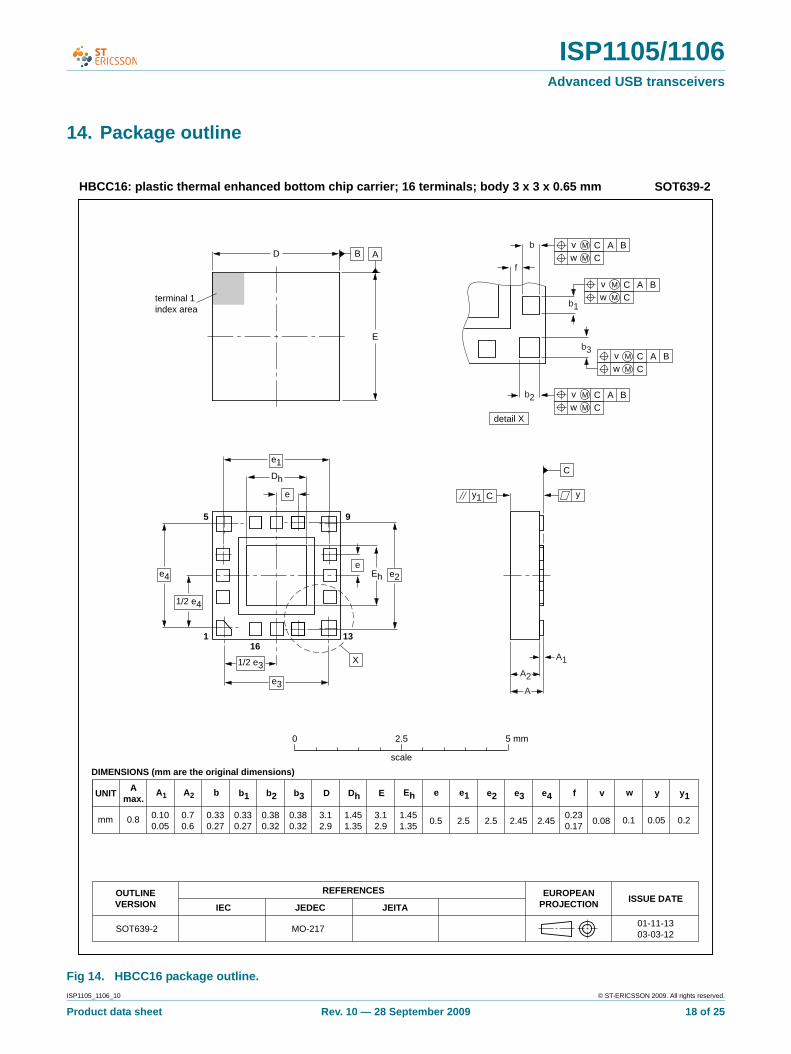
14. Package outline
Fig 14. HBCC16 package outline.
2.5
A1 bA2UNIT D Eh e1
REFERENCESOUTLINEVERSION
EUROPEANPROJECTION ISSUE DATE
01-11-1303-03-12
IEC JEDEC JEITA
mm 0.8 0.100.05
0.70.6
3.12.9
1.451.35
3.12.9
1.451.35
0.330.27
DIMENSIONS (mm are the original dimensions)
SOT639-2 MO-217
Dh
0.330.27
b1
0.380.32
b3
0.380.32
b2
2.45
e3E
0.230.17
f
0.5
we y y1
0.1 0.05 0.22.5
e2
2.45
e4
0.08
v
0 2.5 5 mm
scale
SOT639-2HBCC16: plastic thermal enhanced bottom chip carrier; 16 terminals; body 3 x 3 x 0.65 mm
Amax.
detail X
yy1 C
e
e
e1
e3
Dh
e4
D
E
X
C
B A
161 13
5 9
e2
1/2 e3
1/2 e4
Eh
A1
A2
A
b2
b1
b3
b
f
terminal 1index area
ACC
Bv M
w M
ACC
Bv M
w M
ACC
Bv M
w M
ACC
Bv M
w M
ISP1105_1106_10 © ST-ERICSSON 2009. All rights reserved.
Product data sheet Rev. 10 — 28 September 2009 18 of 25

ISP1105/1106Advanced USB transceivers
Fig 15. HVQFN16 package outline.
terminal 1index area
0.51
A1 EhbUNIT ye
0.2
c
REFERENCESOUTLINEVERSION
EUROPEANPROJECTION ISSUE DATE
IEC JEDEC JEITA
mm 3.12.9
Dh
1.751.45
y1
3.12.9
1.751.45
e1
1.5
e2
1.50.300.18
0.050.00
0.05 0.1
DIMENSIONS (mm are the original dimensions)
SOT758-1 MO-220 - - -- - -
0.50.3
L
0.1
v
0.05
w
0 2.5 5 mm
scale
SOT758-1HVQFN16: plastic thermal enhanced very thin quad flat package; no leads;16 terminals; body 3 x 3 x 0.85 mm
A(1)
max.
AA1
c
detail X
yy1 Ce
L
Eh
Dh
e
e1
b
5 8
16 13
12
94
1
X
D
E
C
B A
e2
02-03-2502-10-21
terminal 1index area
1/2 e
1/2 e
ACC
Bv M
w M
E(1)
Note
1. Plastic or metal protrusions of 0.075 mm maximum per side are not included.
D(1)
ISP1105_1106_10 © ST-ERICSSON 2009. All rights reserved.
Product data sheet Rev. 10 — 28 September 2009 19 of 25

ISP1105/1106Advanced USB transceivers
Fig 16. TSSOP16 package outline.
UNIT A1 A2 A3 bp c D (1) E (2) (1)e HE L Lp Q Zywv θ
REFERENCESOUTLINEVERSION
EUROPEANPROJECTION ISSUE DATE
IEC JEDEC JEITA
mm 0.150.05
0.950.80
0.300.19
0.20.1
5.14.9
4.54.3
0.656.66.2
0.40.3
0.400.06
80
o
o0.13 0.10.21
DIMENSIONS (mm are the original dimensions)
Notes
1. Plastic or metal protrusions of 0.15 mm maximum per side are not included.
2. Plastic interlead protrusions of 0.25 mm maximum per side are not included.
0.750.50
SOT403-1 MO-15399-12-2703-02-18
w Mbp
D
Z
e
0.25
1 8
16 9
θ
AA1
A2
Lp
Q
detail X
L
(A )3
HE
E
c
v M A
XA
y
0 2.5 5 mm
scale
TSSOP16: plastic thin shrink small outline package; 16 leads; body width 4.4 mm SOT403-1
Amax.
1.1
pin 1 index
ISP1105_1106_10 © ST-ERICSSON 2009. All rights reserved.
Product data sheet Rev. 10 — 28 September 2009 20 of 25
ISP1105/1106Advanced USB transceivers
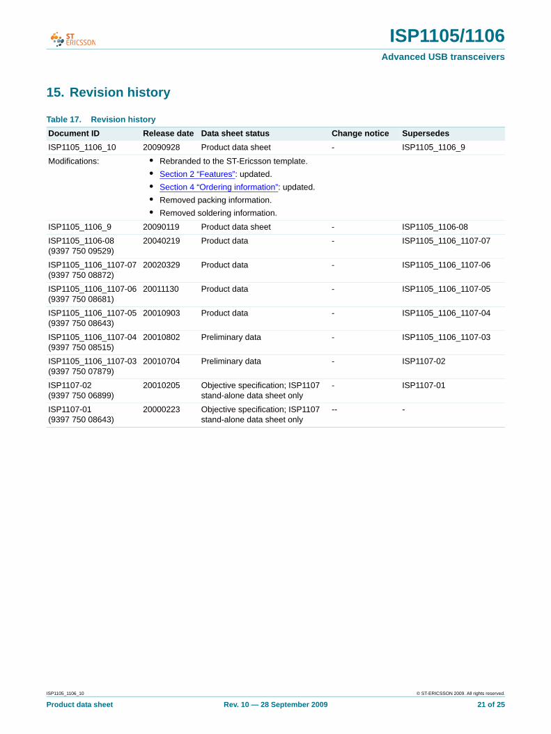
15. Revision history
Table 17. Revision historyDocument ID Release date Data sheet status Change notice SupersedesISP1105_1106_10 20090928 Product data sheet - ISP1105_1106_9
Modifications: • Rebranded to the ST-Ericsson template.• Section 2 “Features”: updated.• Section 4 “Ordering information”: updated.• Removed packing information.• Removed soldering information.
ISP1105_1106_9 20090119 Product data sheet - ISP1105_1106-08
ISP1105_1106-08 (9397 750 09529)
20040219 Product data - ISP1105_1106_1107-07
ISP1105_1106_1107-07 (9397 750 08872)
20020329 Product data - ISP1105_1106_1107-06
ISP1105_1106_1107-06 (9397 750 08681)
20011130 Product data - ISP1105_1106_1107-05
ISP1105_1106_1107-05 (9397 750 08643)
20010903 Product data - ISP1105_1106_1107-04
ISP1105_1106_1107-04 (9397 750 08515)
20010802 Preliminary data - ISP1105_1106_1107-03
ISP1105_1106_1107-03 (9397 750 07879)
20010704 Preliminary data - ISP1107-02
ISP1107-02 (9397 750 06899)
20010205 Objective specification; ISP1107 stand-alone data sheet only
- ISP1107-01
ISP1107-01 (9397 750 08643)
20000223 Objective specification; ISP1107 stand-alone data sheet only
-- -
ISP1105_1106_10 © ST-ERICSSON 2009. All rights reserved.
Product data sheet Rev. 10 — 28 September 2009 21 of 25
ISP1105/1106Advanced USB transceivers
16. Tables
Table 1. Ordering information . . . . . . . . . . . . . . . . . . . . .2Table 2. Selection guide . . . . . . . . . . . . . . . . . . . . . . . . .2Table 3. Pin description . . . . . . . . . . . . . . . . . . . . . . . . . .5Table 4. Function table . . . . . . . . . . . . . . . . . . . . . . . . . .7Table 5. Driving function (pin OE = L) using single-ended
input data interface for ISP1105 (pin MODE = L) . . . . . . . . . . . . . . . . . . . . . . . . .7
Table 6. Driving function (pin OE = L) using differential input data interface for ISP1105 (pin MODE = H) and ISP1106 . . . . . . . . . . . . . . . . . . . . . . . . . . .7
Table 7. Receiving function (pin OE = H) . . . . . . . . . . . .7Table 8. Pin states in disable or sharing mode . . . . . . . .8Table 9. Power supply configuration overview . . . . . . . .8Table 10. Power supply input options . . . . . . . . . . . . . . . .9Table 11. Limiting values . . . . . . . . . . . . . . . . . . . . . . . . . 11Table 12. Recommended operating conditions . . . . . . . . 11Table 13. Static characteristics: supply pins . . . . . . . . . .12Table 14. Static characteristics: digital pins . . . . . . . . . . .13Table 15. Static characteristics: analog I/O pins (D+, D−) 14Table 16. Dynamic characteristics: analog I/O pins
(D+, D−) . . . . . . . . . . . . . . . . . . . . . . . . . . . . . .15Table 17. Revision history . . . . . . . . . . . . . . . . . . . . . . . .21
ISP1105_1106_10 © ST-ERICSSON 2009. All rights reserved.
Product data sheet Rev. 10 — 28 September 2009 22 of 25

ISP1105/1106Advanced USB transceivers
17. Figures
Fig 1. Block diagram (combined ISP1105 and ISP1106). 3Fig 2. Pin configuration ISP1105BSTM (HVQFN).. . . . . .4Fig 3. Pin configuration ISP1105WTS and ISP1105WTM
(HBCC16). . . . . . . . . . . . . . . . . . . . . . . . . . . . . . . .4Fig 4. Pin configuration ISP1106DHTM (TSSOP16).. . . .4Fig 5. Pin configuration ISP1106WTS (HBCC16). . . . . . .4Fig 6. Human Body ESD test model. . . . . . . . . . . . . . . .10Fig 7. Rise and fall times. . . . . . . . . . . . . . . . . . . . . . . .16Fig 8. Timing of OE to D+, D-. . . . . . . . . . . . . . . . . . . . .16Fig 9. Timing of D+, D- to RCV, VP, VM. . . . . . . . . . . . .16Fig 10. Timing of VO/VPO, FSE0/VMO to D+, D-.. . . . . .16Fig 11. Load for enable and disable times. . . . . . . . . . . .17Fig 12. Load for VM, VP and RCV. . . . . . . . . . . . . . . . . .17Fig 13. Load for D+, D-. . . . . . . . . . . . . . . . . . . . . . . . . . .17Fig 14. HBCC16 package outline. . . . . . . . . . . . . . . . . . .18Fig 15. HVQFN16 package outline. . . . . . . . . . . . . . . . . .19Fig 16. TSSOP16 package outline. . . . . . . . . . . . . . . . . .20
ISP1105_1106_10 © ST-ERICSSON 2009. All rights reserved.
Product data sheet Rev. 10 — 28 September 2009 23 of 25

ISP1105/1106Advanced USB transceivers
18. Contents
1 General description . . . . . . . . . . . . . . . . . . . . . . 12 Features . . . . . . . . . . . . . . . . . . . . . . . . . . . . . . . 13 Applications . . . . . . . . . . . . . . . . . . . . . . . . . . . . 24 Ordering information. . . . . . . . . . . . . . . . . . . . . 24.1 Ordering options . . . . . . . . . . . . . . . . . . . . . . . . 25 Block diagram . . . . . . . . . . . . . . . . . . . . . . . . . . 36 Pinning information. . . . . . . . . . . . . . . . . . . . . . 46.1 Pinning . . . . . . . . . . . . . . . . . . . . . . . . . . . . . . . 46.2 Pin description . . . . . . . . . . . . . . . . . . . . . . . . . 57 Functional description . . . . . . . . . . . . . . . . . . . 77.1 Function selection. . . . . . . . . . . . . . . . . . . . . . . 77.2 Operating functions . . . . . . . . . . . . . . . . . . . . . 77.3 Power supply configurations. . . . . . . . . . . . . . . 87.4 Power supply input options. . . . . . . . . . . . . . . . 98 Electrostatic discharge (ESD). . . . . . . . . . . . . 108.1 ESD protection . . . . . . . . . . . . . . . . . . . . . . . . 108.2 ESD test conditions . . . . . . . . . . . . . . . . . . . . 109 Limiting values. . . . . . . . . . . . . . . . . . . . . . . . . 1110 Recommended operating conditions. . . . . . . 1111 Static characteristics. . . . . . . . . . . . . . . . . . . . 1212 Dynamic characteristics . . . . . . . . . . . . . . . . . 1513 Test information. . . . . . . . . . . . . . . . . . . . . . . . 1714 Package outline . . . . . . . . . . . . . . . . . . . . . . . . 1815 Revision history. . . . . . . . . . . . . . . . . . . . . . . . 2116 Tables . . . . . . . . . . . . . . . . . . . . . . . . . . . . . . . . 2217 Figures . . . . . . . . . . . . . . . . . . . . . . . . . . . . . . . 2318 Contents . . . . . . . . . . . . . . . . . . . . . . . . . . . . . . 24
ISP1105_1106_10 © ST-ERICSSON 2009. All rights reserved.
Product data sheet Rev. 10 — 28 September 2009 24 of 25

ISP1105/1106Advanced USB transceivers
Please Read Carefully:
The contents of this document are subject to change without prior notice. ST-Ericsson makes no representation or warranty of any naturewhatsoever (neither expressed nor implied) with respect to the matters addressed in this document, including but not limited to warranties ofmerchantability or fitness for a particular purpose, interpretability or interoperability or, against infringement of third party intellectual propertyrights, and in no event shall ST-Ericsson be liable to any party for any direct, indirect, incidental and or consequential damages and or losswhatsoever (including but not limited to monetary losses or loss of data), that might arise from the use of this document or the information in it.
ST-Ericsson and the ST-Ericsson logo are trademarks of the ST-Ericsson group of companies or used under a license from STMicroelectronics NV or Telefonaktiebolaget LM Ericsson.
All other names are the property of their respective owners.
© ST-Ericsson, 2009 - All rights reserved
Contact information at www.stericsson.com under Contacts
www.stericsson.com
ISP1105_1106_10 © ST-ERICSSON 2009. All rights reserved.
Product data sheet Rev. 10 — 28 September 2009 25 of 25