UNIT -I INTRODUCTION TO ASICS, CMOS LOGIC, ASIC … · specific application so, we might call some...
174
UNIT -I INTRODUCTION TO ASICS, CMOS LOGIC, ASIC LIBRARY DESIGN
-
Upload
trankhuong -
Category
Documents
-
view
219 -
download
3
Transcript of UNIT -I INTRODUCTION TO ASICS, CMOS LOGIC, ASIC … · specific application so, we might call some...
UNIT -IINTRODUCTION TO ASICS, CMOS
LOGIC, ASIC LIBRARY DESIGN
Introduction
• ASIC [“a-sick”] is an acronym for Application Specific Integrated Circuit.
• As the name indicates, ASIC is a non-standard integrated circuit that is designed for a specific use or application.
• Generally an ASIC design will be undertaken for a product that will have a large production run , and the ASIC may contain a very large part of the electronics needed on a single integrated circuit.
Contd..• Examples for ASIC Ics are : a chip for a toy bear that talks; a
chip for a satellite; a chip designed to handle the interfacebetween memory and a microprocessor for a workstation CPU;and a chip containing a microprocessor as a cell together withother logic.
Contd..
• Two ICs that might or might not be considered as ASICs are, acontroller chip for a PC and a chip for a modem. Both of theseexamples are specific to an application (shades of an ASIC)but are sold to many different system vendors (shades of astandard part). ASICs such as these are sometimes calledapplication-specific standard products ( ASSPs ).
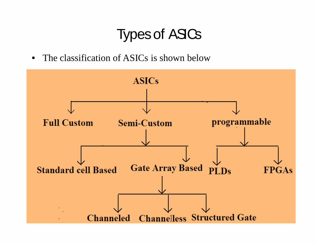
Types of ASICs• The classification of ASICs is shown below
Contd..• So, as shown in the slide the ASICs are broadly classified into
three types.• I. Full-Custom ASICs• II. Semi-custom ASICs• III. Programmable ASICs
Full-Custom ASICs• A Full custom ASIC is one which includes some (possibly all)
logic cells that are customized and all mask layers that arecustomized.
• A microprocessor is an example of a full-custom IC . Designersspend many hours squeezing the most out of every last squaremicron of microprocessor chip space by hand.
• Customizing all of the IC features in this way allows designersto include analog circuits, optimized memory cells, ormechanical structures on an IC, for example. Full-custom ICsare the most expensive to manufacture and to design.
Contd..• The manufacturing lead time (the time required just to make
an IC not including design time) is typically eight weeks for afull-custom IC.
• These specialized full-custom ICs are often intended for aspecific application so, we might call some of them as full-custom ASICs.
Contd…
• In a full-custom ASIC an engineer designs some or all of thelogic cells, circuits, or layout specifically for one ASIC. Thismeans the designer avoids using pretested and pre characterizedcells for all or part of that design.
• This might be because existing cell libraries are not fast enough,or the logic cells are not small enough or consume too muchpower.
Contd…• One has to use full-custom design if the ASIC technology is
new or so specialized that there are no existing cell libraries orbecause the ASIC is so specialized that some circuits must becustom designed.
• Fewer and fewer full-custom ICs are being designed becauseof the problems with these special parts of the ASIC.
• The growing member of this family, now a days is themixed analog/digital ASIC,
Semicustom ASICs• ASICs , for which all of the logic cells are predesigned and some (possibly
all) of the mask layers are customized are called semi custom ASICs.• Using the predesigned cells from a cell library makes the design , much
easier.• There are two types of semicustom ASICs
• (i) Standard-cell–based ASICs (ii)Gate-array–based ASICs.
Standard-Cell Based ASICs• A cell-based ASIC (cell-based IC, or CBIC pronounced sea-bick)
uses predesigned logic cells (AND gates, OR gates,multiplexers, and flip-flops, for example) known as standardcells.
• One can apply the term CBIC to any IC that uses cells, but itis generally accepted that a cell-based ASIC or CBIC means astandard-cell based ASIC.
Contd…• The standard-cell areas (also called flexible blocks) in a CBIC
are built of rows of standard cells like a wall built of bricks.The standard-cell areas may be used in combination withmicrocontrollers or even microprocessors, known as megacells. Mega cells are also called mega functions, full-customblocks, system-level macros (SLMs), fixed blocks, cores, orFunctional Standard Blocks (FSBs).
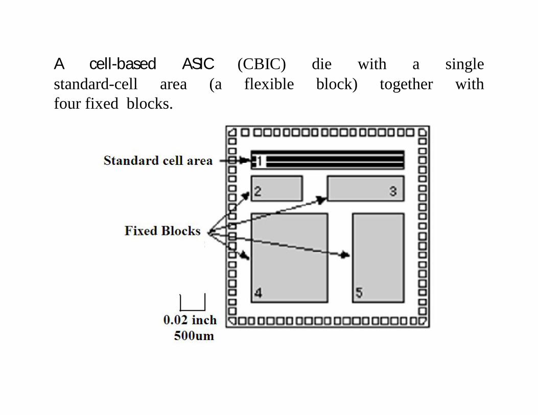
A cell-based ASIC (CBIC) die with a singlestandard-cell area (a flexible block) together withfour fixed blocks.
Contd…• The ASIC designer defines only the placement of the standard
cells and the interconnect in a CBIC. However, the standardcells can be placed anywhere on the silicon; this means that allthe mask layers of a CBIC are customized and are unique to aparticular customer.
• The advantage of CBICs is that designers save time, money,and reduce risk by using a predesigned, pretested, and precharacterized standard-cell library.
• In addition each standard cell can be optimized individually.During the design of the cell library each and every transistorin every standard cell can be chosen to maximize speed orminimize area .
Contd…
• The disadvantages are the time or expense of designing orbuying the standard-cell library and the time needed tofabricate all layers of the ASIC for each new design.
Gate-Array Based ASICs• In a gate array (sometimes abbreviated GA) or gate-array
based ASIC the transistors are predefined on the silicon wafer.• The predefined pattern of transistors on a gate array is the base
array , and the smallest element that is replicated to make thebase array is the base cell (sometimes called a primitive cell ).
Contd…• Only the top few layers of metal, which define the interconnect
between transistors, are defined by the designer using custommasks. To distinguish this type of gate array from other typesof gate array, it is often called a masked gate array ( MGA ).
• The designer chooses from a gate-array library of predesigned and pre-characterized logic cells
Contd…
• The logic cells in a gate-array library are often called macros .The reason for this is that the base-cell layout is the same foreach logic cell, and only the interconnect (inside cells andbetween cells) is customized, which is similar to a softwaremacro.
Types of MGA or Gate-array based ASICs
• There are three types of Gate Array based ASICs.• Channeled gate arrays.• Channelless gate arrays.• Structured gate arrays.
Channeled gate arrays
• The channeled gate array was the first to be developed . In achanneled gate array space is left between the rows oftransistors for wiring.
• A channeled gate array is similar to a CBIC. Both use the rowsof cells separated by channels used for interconnect. Onedifference is that the space for interconnect between rows ofcells are fixed in height in a channeled gate array, whereas thespace between rows of cells may be adjusted in a CBIC.
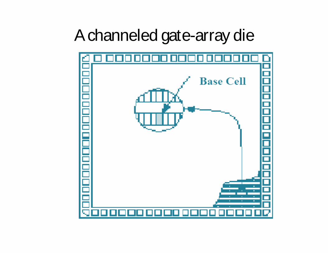
A channeled gate-array die
Features of MGA • Only the interconnect is customized.• The interconnect uses predefined spaces between rows of base
cells.• Manufacturing lead time is between two days and two weeks.
Channel less Gate Array
• This channel less gate-array architecture is now more widelyused . The routing on a channelless gate array uses rows ofunused transistors.
• The key difference between a channel less gate array andchanneled gate array is that there are no predefined areas setaside for routing between cells on a channel less gate array.Instead we route over the top of the gate-array devices. Wecan do this because we customize the contact layer that definesthe connections between metal 1, the first layer of metal, andthe transistors.
Features of Channel less Gate Array• Only the interconnect is customized.• The interconnect uses predefined spaces between rows of base
cells.• Manufacturing lead time is around two days to two weeks.• When we use an area of transistors for routing in a channel
less array, we do not make any contacts to the devices lying underneath , we simply leave the transistors unused.
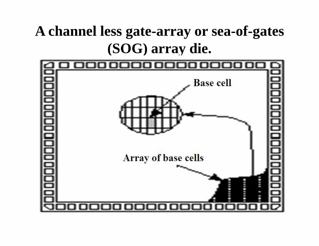
A channel less gate-array or sea-of-gates (SOG) array die.
Contd…• The basic difference between a channel less gate array and
channeled gate array is that there are no predefined areas setaside for routing between cells on a channel less gate array.Instead we route over the top of the gate-array devices.
• It is done like this because we customize the contact layer thatdefines the connections between metal1, the first layer ofmetal, and the transistors. When we use an area of transistorsfor routing in a channel less array, we do not make anycontacts to the devices lying underneath; we simply leave thetransistors unused.
Contd…• The logic density ,the amount of logic that can be implemented
in a given silicon area is higher for channel less gate arraysthan for channeled gate arrays. This is usually attributed to thedifference in structure between the two types of array. In fact,the difference occurs because the contact mask is customizedin a channel less gate array, but is not usually customized in achanneled gate array. This leads to denser cells in the channelless architectures. Customizing the contact layer in a channelless gate array allows us to increase the density of gate-arraycells because we can route over the top of unused contact sites.
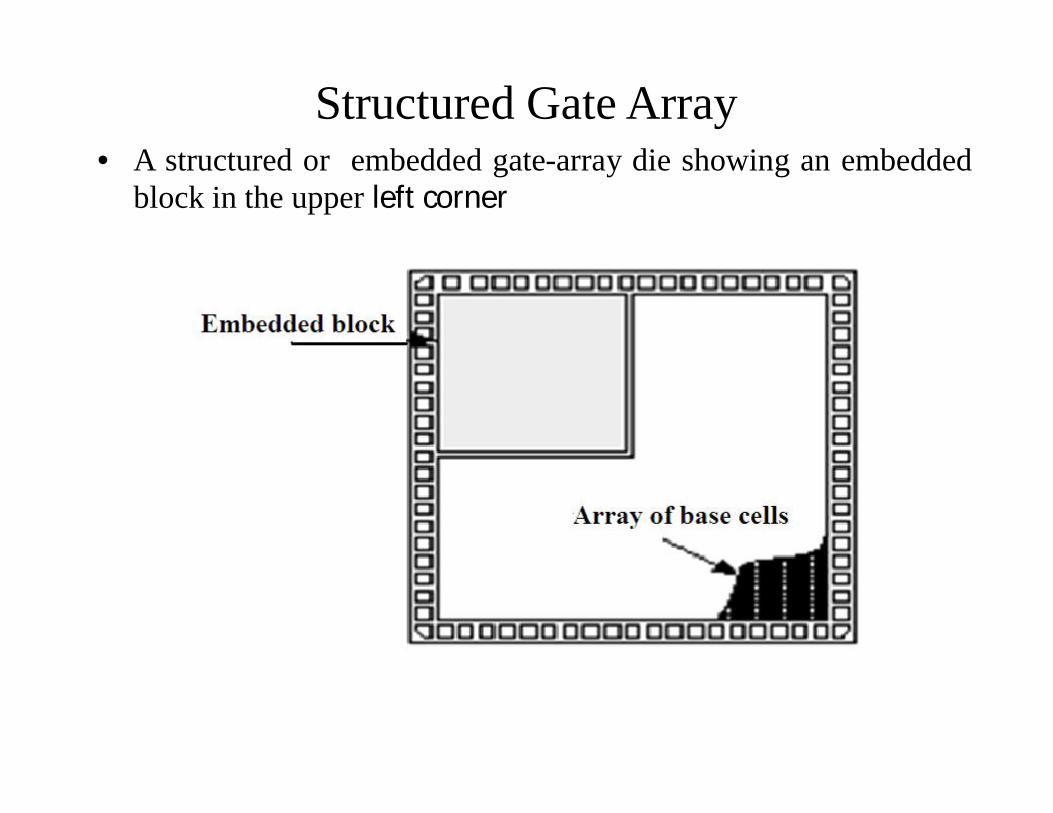
Structured Gate Array• A structured or embedded gate-array die showing an embedded
block in the upper left corner
Feature Of Structured Gate Array
• Only the interconnect is customized• Custom Blocks(same for each design can be embedded)• Manufacturing lead time is between two days and two weeks.• An embedded gate array gives the improved area efficiency
and increased performance of a CBIC but with the lower costand faster turn around of an MGA.
• The disadvantage of an embedded gate array is that theembedded function is fixed.
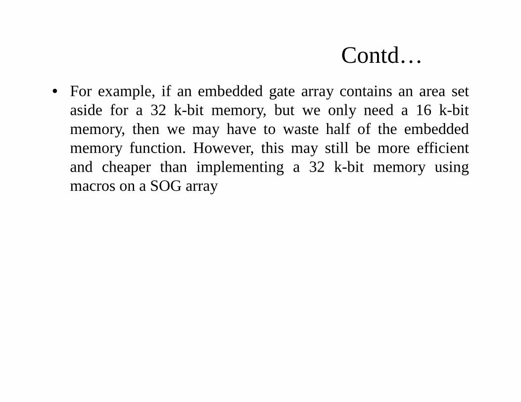
Contd…• For example, if an embedded gate array contains an area set
aside for a 32 k-bit memory, but we only need a 16 k-bitmemory, then we may have to waste half of the embeddedmemory function. However, this may still be more efficientand cheaper than implementing a 32 k-bit memory usingmacros on a SOG array
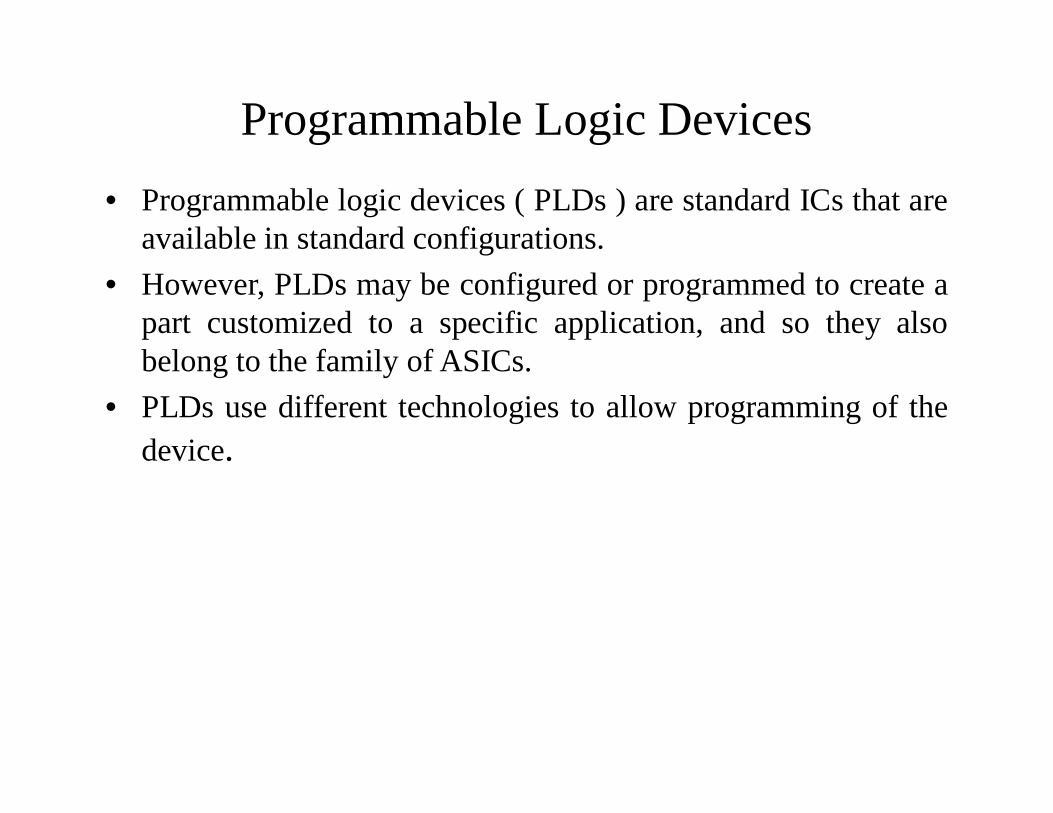
Programmable Logic Devices• Programmable logic devices ( PLDs ) are standard ICs that are
available in standard configurations.• However, PLDs may be configured or programmed to create a
part customized to a specific application, and so they alsobelong to the family of ASICs.
• PLDs use different technologies to allow programming of thedevice.
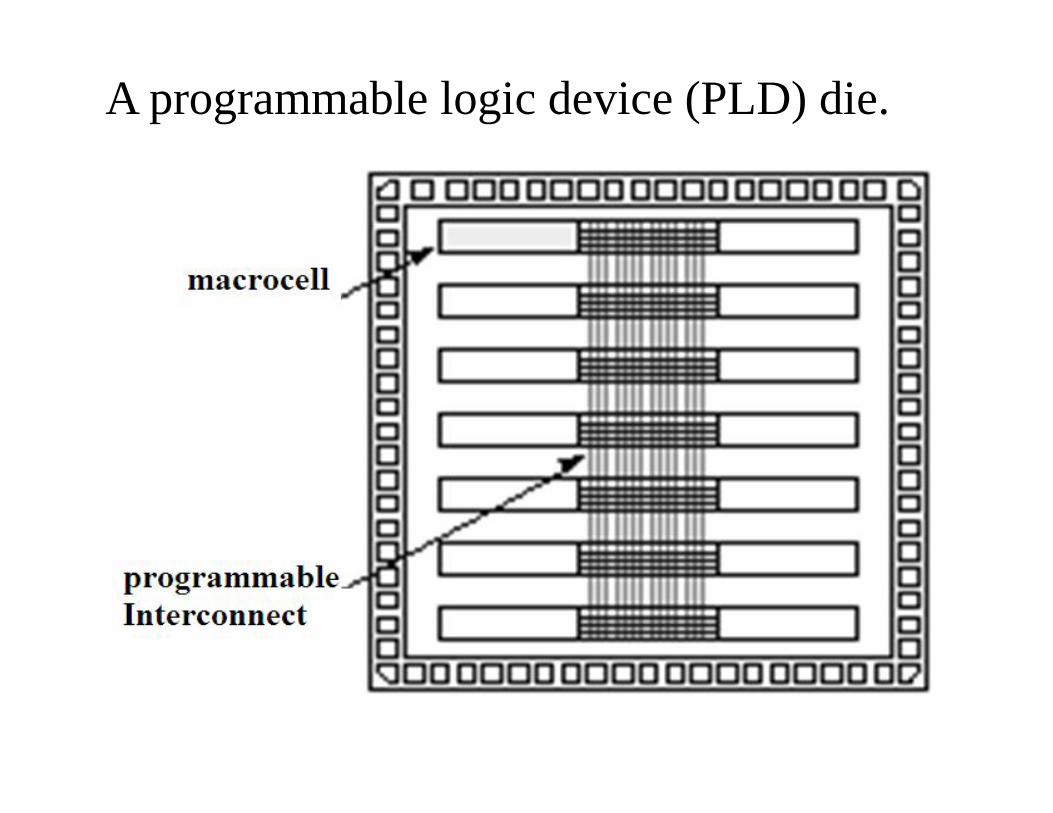
A programmable logic device (PLD) die.
Features of PLDs • No customized mask layers or logic cells• Fast design turnaround• A single large block of programmable interconnect• A matrix of logic macro cells that usually consist of
programmable array logic followed by a flip-flop or latch
Contd…
• The simplest type of programmable IC is a read-only memory(ROM ). The most common types of ROM use a metal fuse thatcan be blown permanently (a programmable ROM or PROM ).
• An electrically programmable ROM , or EPROM , usesprogrammable MOS transistors whose characteristics arealtered by applying a high voltage.
Contd…• One can erase an EPROM either by using another high
voltage (an electrically erasable PROM , or EEPROM ) or byexposing the device to ultraviolet light (UV-erasable PROM,or UVPROM).
• There is another type of ROM that can be placed on any ASICa mask-programmable ROM (mask-programmed ROM ormasked ROM). A masked ROM is a regular array oftransistors permanently programmed using custom maskpatterns.
• So, an embedded masked ROM is a large,specialized, logic cell.
Field-Programmable Gate Arrays(FPGAs)• FPGAs are the newest member of the ASIC family and are
rapidly growing in , replacing TTL in microelectronic systems.Even though an FPGA is a type of gate array, we do notconsider the term gate-array based ASICs to include FPGAs.
• There is very little difference between an FPGA and a PLD.An FPGA is usually just larger and more complex than aPLD. In fact, some vendors that manufacture programmableASICs call their products as FPGAs and some call them ascomplex PLDs .
Characteristics of an FPGA• None of the mask layers are customized.• There is a method for programming the basic logic cells and
the interconnect.• The core is a regular array of programmable basic logic cells
that can implement combinational as well as sequential logic (flip-flops).
• A matrix of programmable interconnect surrounds the basic logic cells.
• Programmable I/O cells surround the core.• Design turnaround is a few hours.
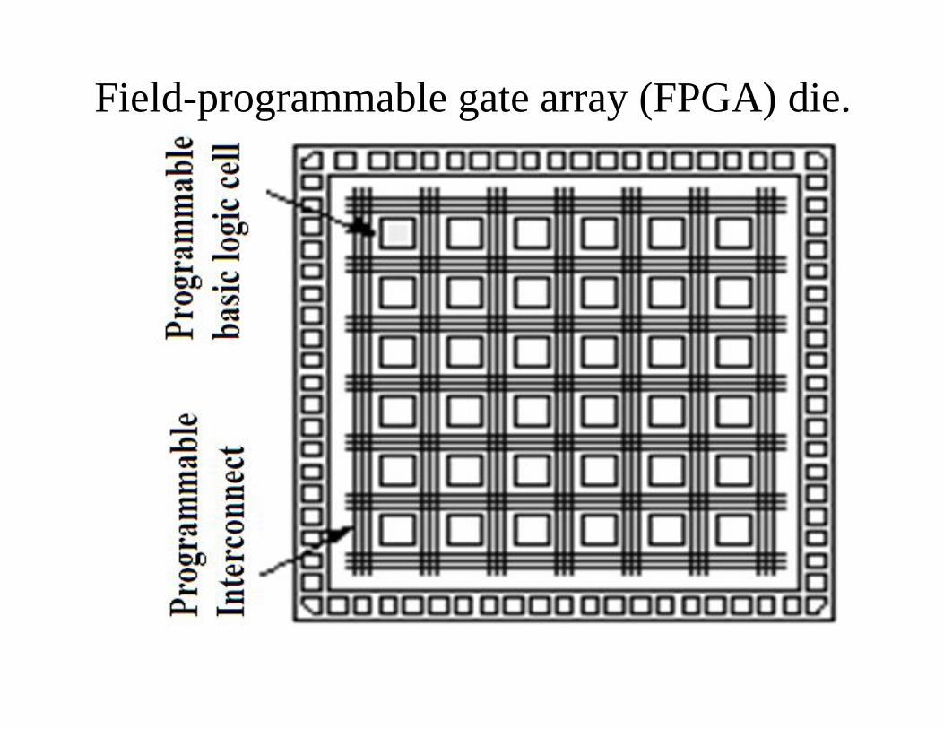
Field-programmable gate array (FPGA) die.
Contd…• The architecture consists of configurable logic blocks,
configurable I/O blocks, and programmable interconnect.Also, there will be clock circuitry for driving the clock signalsto each logic block, and additional logic resources such asALUs, memory, and decoders may be available. The twobasic types of programmable elements for an FPGA are Static
RAM and anti-fuses.
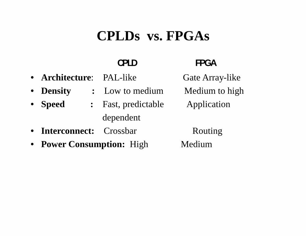
CPLDs vs. FPGAs
CPLD FPGA• Architecture: PAL-like Gate Array-like• Density : Low to medium Medium to high• Speed : Fast, predictable Application
dependent • Interconnect: Crossbar Routing• Power Consumption: High Medium
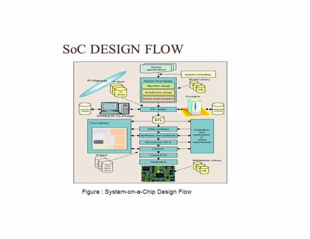
Design Flow• The sequence of steps to design an ASIC is known as the
Design flow . The various steps involved in ASIC design floware given below.
1. Design entry : Design entry is a stage where the microarchitecture is implemented in a Hardware Descriptionlanguage like VHDL, Verilog , System Verilog etc.In early days , a schematic editor was used for design entrywhere designers instantiated gates. Increased complexity inthe current designs require the use of HDLs to gainproductivity . Another advantage is that HDLs areindependent
.
Contd…
2. Logic synthesis: Use an HDL (VHDL or Verilog) and a logic synthesis tool to produce a net list a description of the logic cells and their connections
3.System partitioning : Divide a large system into ASIC-sized pieces.
4. Pre-layout simulation: Check to see if the design functions correctly.
5. Floor planning: Arrange the blocks of the netlist on the chip.6. Placement: Decide the locations of cells in a block.7. Routing: Make the connections between cells and blocks.
Contd…8.Extraction : Determine the resistance and capacitance of
the interconnect.9. Post layout simulation. It is used to check to see whether the
design still works with the added loads of the interconnect ornot
The flow diagram is shown in the next slide.
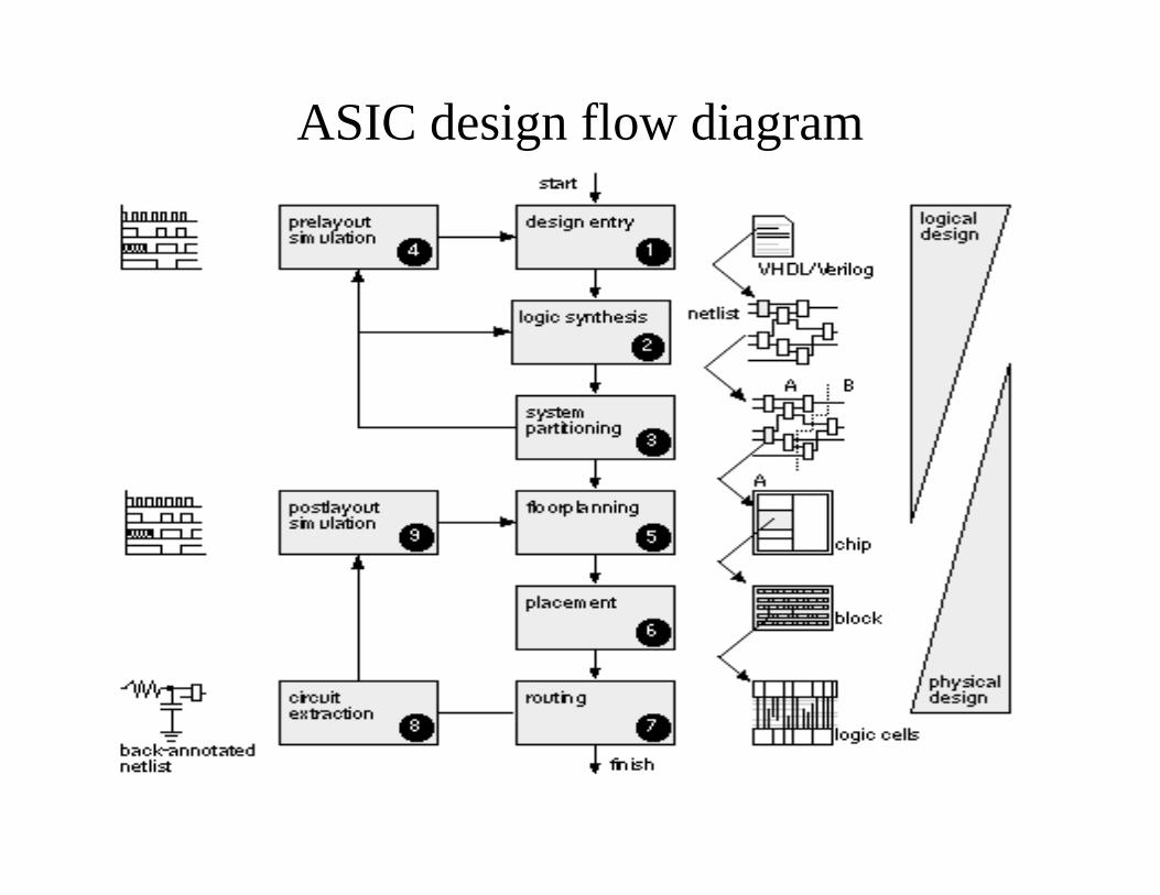
ASIC design flow diagram
Contd…• In the flow diagram the steps from 1 to 4 are part of logical
design ,and steps from 5 to 9 are part of physical design.
• When we are performing system partitioning we have to consider both logical and physical factors.
CMOS Design Rules• The design rules are Interface between designer and process
engineer and guidelines for constructing process masks• The figures in the next slides defines the design rules for a
CMOS process using pictures. Arrows between objects denotea minimum spacing, and arrows showing the size of an objectdenote a minimum width.
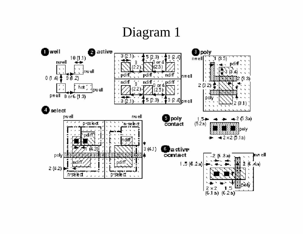
Diagram 1
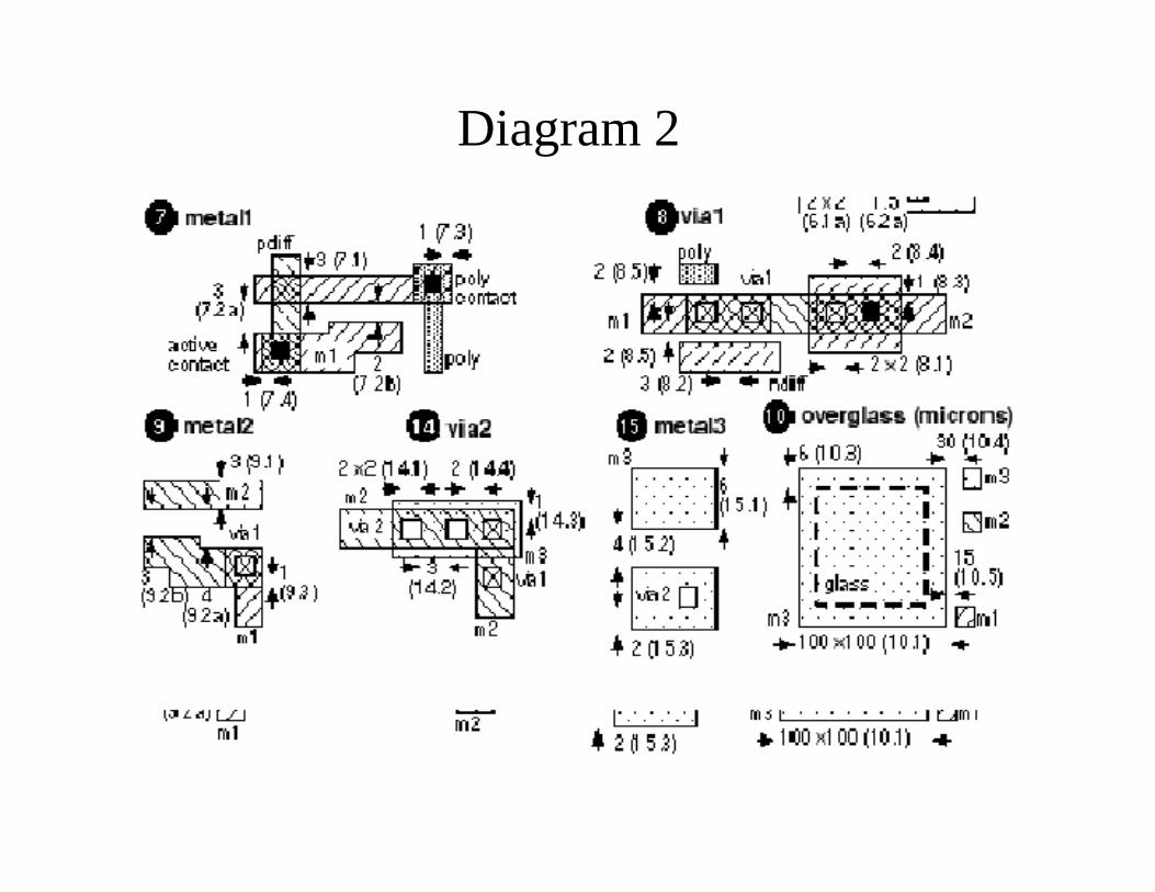
Diagram 2
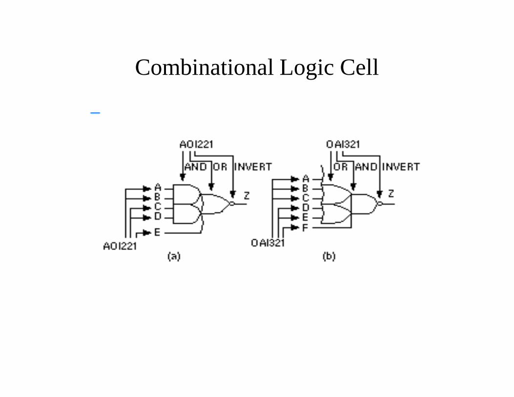
Combinational Logic Cell
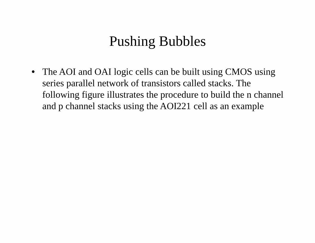
Pushing Bubbles
• The AOI and OAI logic cells can be built using CMOS using series parallel network of transistors called stacks. The following figure illustrates the procedure to build the n channel and p channel stacks using the AOI221 cell as an example
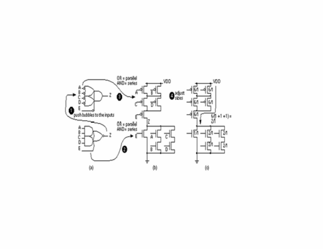
Transmission Gate
• The following figure shows the CMOS transmission gate (TG,Tx gate,pass gate,coupler) We connect a p channel transistor(to transmit a strong 1) in parallel with a n channel transistor(to transmit a strong 0)
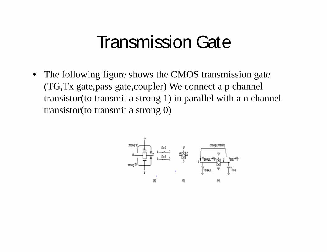
Transistor as Resistors
Junction Capacitance
• The junction capacitances, C BD and C BS , consist of two parts: junction area and sidewall; both have different physical characteristics with parameters CJ and MJ for the junction, CJSW and MJSW for the sidewall, and PB is common. These capacitances depend on the voltage across the junction ( V DB and V SB ).
Overlap Capacitance
• The overlap capacitance account for lateral diffusion (the amount the source and drain extend under the gate) using SPICE parameter LD = 5E-08 or L D = 0.05 m m.
• Not all versions of SPICE use the equivalent parameter for width reduction, WD in calculating C GDOV and not all versions subtract W D to form W EFF .
Gate Capacitance
• The gate–bulk capacitance C GB may be viewed as two capacitors in series: the fixed gate-oxide capacitance, C O = W EFFL EFF e ox / T ox . Variable depletion Capacitance, C S = W EFF L EFF e Si / x d , formed by the depletion region that extends under the gate (with varying depth x d ).
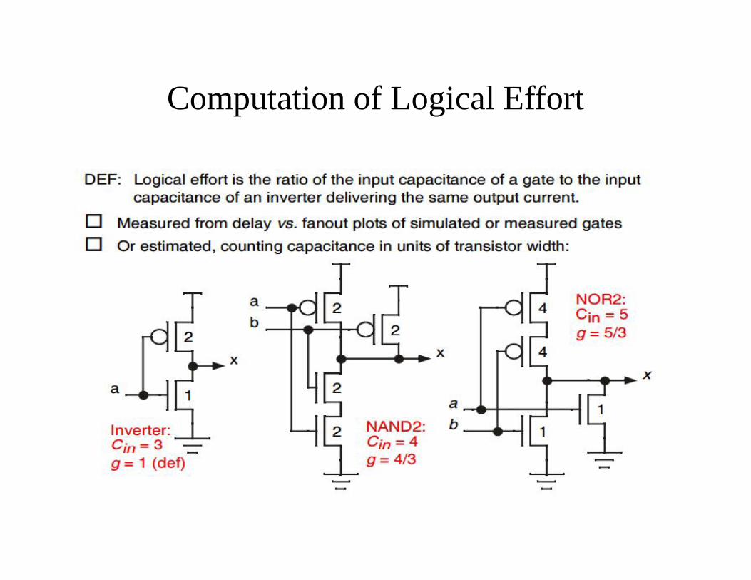
Computation of Logical Effort
Library –Cell Design
• The optimum cell layout for each process generation changes because the design rules for each ASIC vendor’s process are always slightly different—even for the same generation of technology. For example, two companies may have very similar 0.35 m m CMOS process technologies, but the third-level metal spacing might be slightly different.
• If a cell library is to be used with both processes, we could construct the library by adopting the most stringent rules from each process.
•
Library – Cell Design(Cont)
• A library constructed in this fashion may not be competitive with one that is constructed specifically for each process.
• The reason that most vendors have similar rules is because most vendors use the same manufacturing equipment and a similar process. It is possible to construct a highest common denominator library that extracts the most from the current manufacturing capability
Cont• Layout of library cells is either hand-crafted or uses
some form of symbolic layout . • Symbolic layout is usually performed in one of two
ways: using either interactive graphics or a text layout language. Shapes are represented by simple lines or rectangles, known as sticks or logs , in symbolic layout. The actual dimensions of the sticks or logs are determined after layout is completed in a post processing step.
Cont• An alternative to graphical symbolic layout uses a text layout
language, similar to a programming language such as C, that directs a program to assemble layout. The spacing and dimensions of the layout shapes are defined in terms of variables rather than constants. These variables can be changed after symbolic layout is complete to adjust the layout spacing to a specific process.
• As libraries get larger, and the capability to quickly move libraries and ASIC designs between different generations of process technologies becomes more important, the advantages of symbolic layout may outweigh the disadvantage
UNIT - II
PROGRAMMABLE ASICS, PROGRAMMABLE ASIC
LOGIC CELLS
Programmable ASICs
• Two basic types of programmable ASICs– Programmable Logic Device (PLD) - first developed as
small programmable devices that can replace a handful of TTL parts
• least complex ones are a simple AND/OR PLA with latches on the outputs and feedback paths to the inputs of the array
– Field Programmable Gate Array (FPGA) - more complex devices that can hold up to 100K gate equivalents or more
• some implemented as symmetrical arrays of simple logic devices
• others include more complex and specialized logic blocks
• Automatic tools create a string of bits (a configuration file) describing the extra connections necessary to program the FPGA to perform the required function
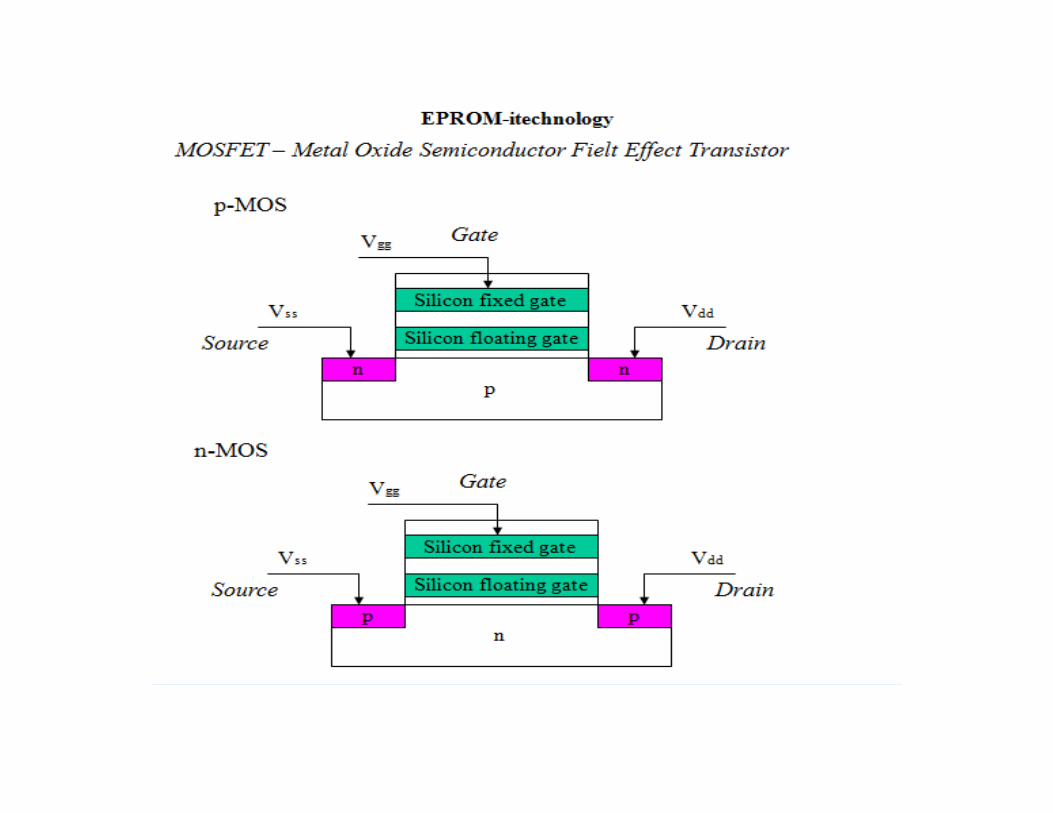
Programming Technologies
• Static RAM cells- Flipflops of static RAM• Anti-fuse – Burnable Joints• EPROM (Erasable Programmable Read Only
Memory),EEPROM(Electrically Erasable Programmable Read Only Memory) and Flash ROM elements commanded by floating gate
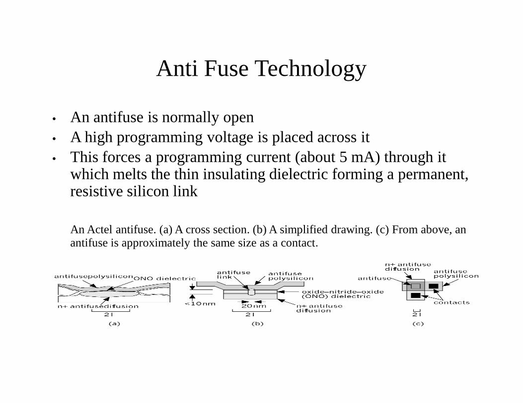
Anti Fuse Technology
• An antifuse is normally open• A high programming voltage is placed across it• This forces a programming current (about 5 mA) through it
which melts the thin insulating dielectric forming a permanent, resistive silicon link
An Actel antifuse. (a) A cross section. (b) A simplified drawing. (c) From above, an antifuse is approximately the same size as a contact.
• An Actel antifuse. (a) A cross section. (b) A simplified drawing. (c) From above, an antifuse is approximately the same size as a contact.
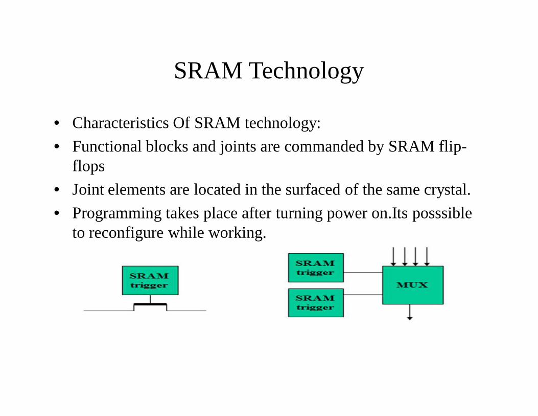
SRAM Technology
• Characteristics Of SRAM technology:• Functional blocks and joints are commanded by SRAM flip-
flops• Joint elements are located in the surfaced of the same crystal.• Programming takes place after turning power on.Its posssible
to reconfigure while working.
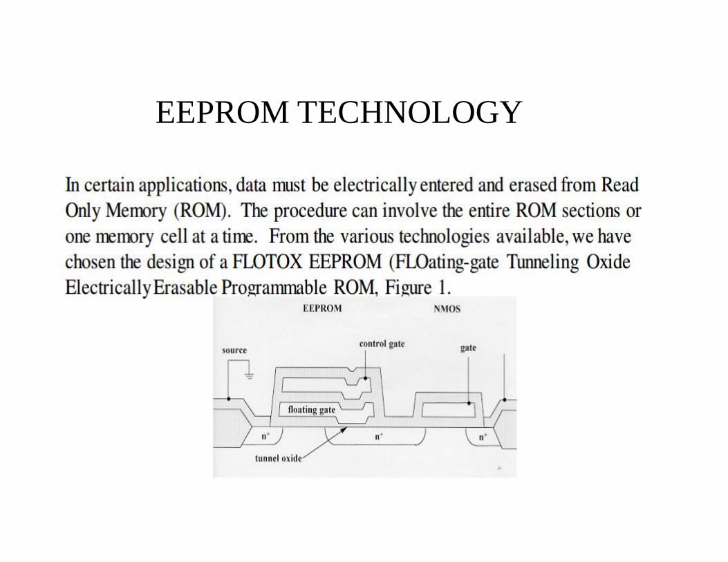
EEPROM TECHNOLOGY
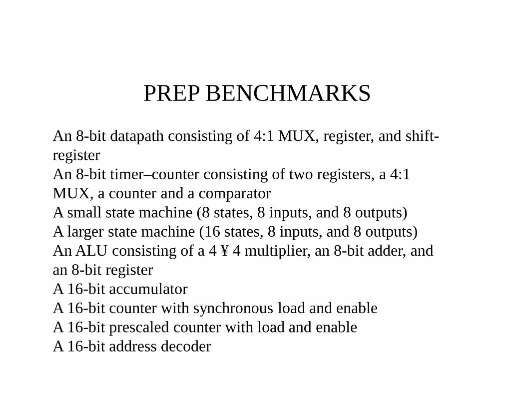
An 8-bit datapath consisting of 4:1 MUX, register, and shift-registerAn 8-bit timer–counter consisting of two registers, a 4:1 MUX, a counter and a comparatorA small state machine (8 states, 8 inputs, and 8 outputs)A larger state machine (16 states, 8 inputs, and 8 outputs)An ALU consisting of a 4 ¥ 4 multiplier, an 8-bit adder, and an 8-bit registerA 16-bit accumulatorA 16-bit counter with synchronous load and enableA 16-bit prescaled counter with load and enableA 16-bit address decoder
PREP BENCHMARKS
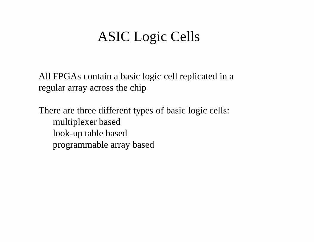
ASIC Logic Cells
All FPGAs contain a basic logic cell replicated in a regular array across the chip
There are three different types of basic logic cells:multiplexer basedlook-up table basedprogrammable array based
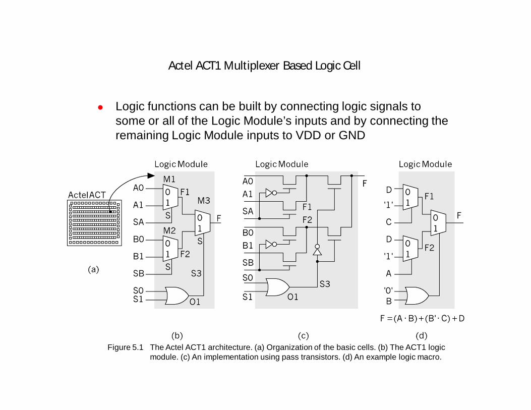
Actel ACT1 Multiplexer Based Logic Cell
Logic functions can be built by connecting logic signals to some or all of the Logic Module’s inputs and by connecting the remaining Logic Module inputs to VDD or GND
Figure 5.1 The Actel ACT1 architecture. (a) Organization of the basic cells. (b) The ACT1 logic module. (c) An implementation using pass transistors. (d) An example logic macro.
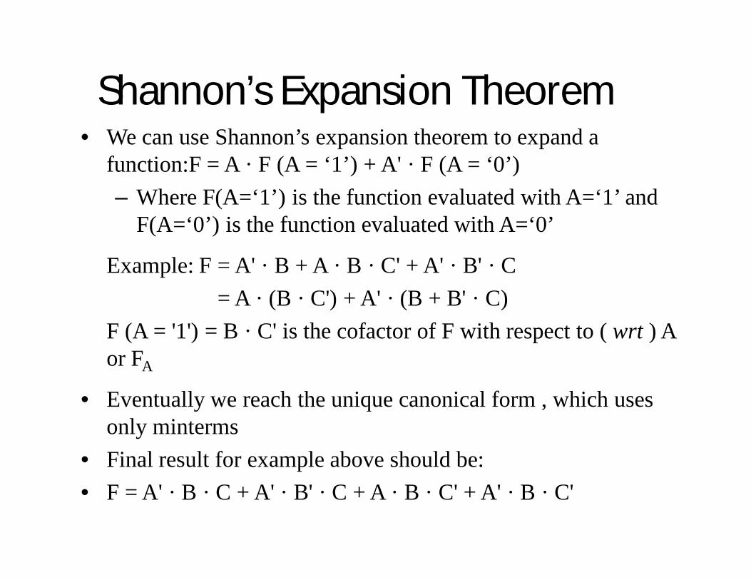
Shannon’s Expansion Theorem• We can use Shannon’s expansion theorem to expand a
function:F = A · F (A = ‘1’) + A' · F (A = ‘0’)– Where F(A=‘1’) is the function evaluated with A=‘1’ and
F(A=‘0’) is the function evaluated with A=‘0’
Example: F = A' · B + A · B · C' + A' · B' · C= A · (B · C') + A' · (B + B' · C)
F (A = '1') = B · C' is the cofactor of F with respect to ( wrt ) A or FA
• Eventually we reach the unique canonical form , which uses only minterms
• Final result for example above should be:• F = A' · B · C + A' · B' · C + A · B · C' + A' · B · C'
Boolean Functions of Two Variables Using a 2:1 Mux
Function, F F = Canonical form Minterms Mintermcode
Functionnumber
M1A0 A1 SA
1 '0' '0' '0' none 0000 0 0 0 02 NOR1-1(A, B) (A + B') A' · B 1 0010 2 B 0 A3 NOT(A) A' A' · B' + A' · B 0, 1 0011 3 0 1 A4 AND1-1(A, B) A · B' A · B' 2 0100 4 A 0 B5 NOT(B) B' A' · B' + A · B' 0, 2 0101 5 0 1 B6 BUF(B) B A' · B + A · B 1, 3 1010 6 0 B 17 AND(A, B) A · B A · B 3 1000 8 0 B A8 BUF(A) A A · B' + A · B 2, 3 1100 9 0 A 19 OR(A, B) A + B A' · B + A · B' + A · B 1, 2, 3 1110 13 B 1 A10 '1' '1' A' · B' + A' · B + A · B' + A · B 0, 1, 2, 3 1111 15 1 1 1
ACT1 LM as a Function Wheel (cont.)
• A 2:1 MUX is a function wheel that can generate BUF, INV, AND-11, AND1-1, OR, AND
• Define a function WHEEL (A, B) = MUX (A0, A1, SA)• MUX (A0, A1, SA) = A0 · SA' + A1 · SA• Each of the inputs (A0, A1, and SA) may be A, B, '0', or '1'• The ACT 1 LM is built from two function wheels, a 2:1 MUX,
and a two-input OR gate:
ACT 1 LM = MUX [WHEEL1, WHEEL2, OR (S0, S1)]
ACT1 LM as a Function Wheel
Figure 5.3 The ACT1 logic module as a boolean function generator. (a) A 2:1 MUX viewed as a logic wheel. (b) The ACT1 logic module viewed as two function wheels.
Example of Implementing a Function with an ACT1 LM
• Example of using the WHEEL functions to implement:F = NAND (A, B) = (A · B)’
1. First express F as the output of a 2:1 MUX: expand F wrt A (or wrt B; since F is symmetric)
F = A · (B') + A' · ('1')
2. Assign WHEEL1 to implement INV (B), and WHEEL2 to implement '1'
3. Set the select input to the MUX connecting WHEEL1 and WHEEL2, S0 + S1 = A. We can do this using S0 = A, S1 = '1'
• A single Actel ACT1 LM can implement all combinational two-input functions, most three input functions and many four input functions
• A transparent D latch can be implemented with one ACT1 LM and an edge triggered D flip-flop can be implemented with two LM’s
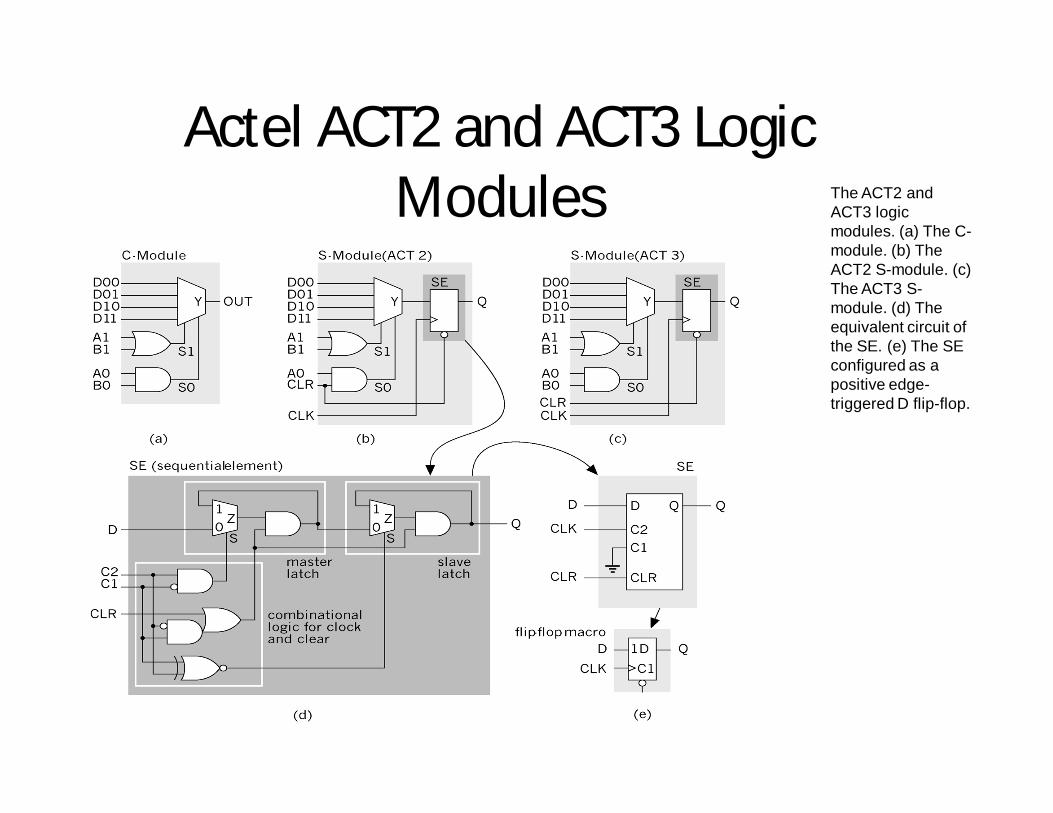
Actel ACT2 and ACT3 Logic Modules The ACT2 and
ACT3 logic modules. (a) The C-module. (b) The ACT2 S-module. (c) The ACT3 S-module. (d) The equivalent circuit of the SE. (e) The SE configured as a positive edge-triggered D flip-flop.
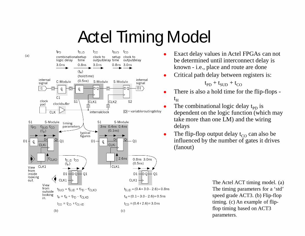
Actel Timing Model Exact delay values in Actel FPGAs can not
be determined until interconnect delay is known - i.e., place and route are done
Critical path delay between registers is:tPD + tSUD + tCO
There is also a hold time for the flip-flops -tH
The combinational logic delay tPD is dependent on the logic function (which may take more than one LM) and the wiring delays
The flip-flop output delay tCO can also be influenced by the number of gates it drives (fanout)
The Actel ACT timing model. (a) The timing parameters for a ‘std’ speed grade ACT3. (b) Flip-flop timing. (c) An example of flip-flop timing based on ACT3 parameters.
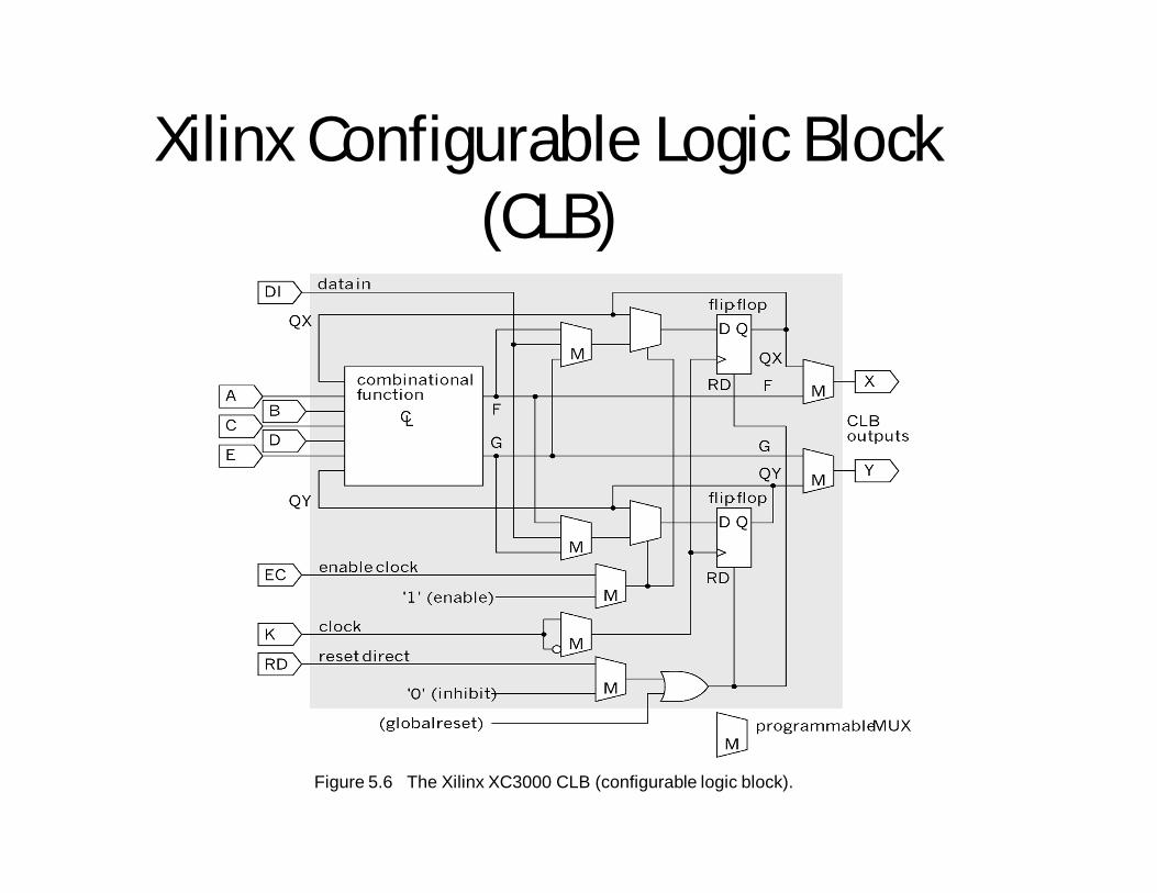
Xilinx Configurable Logic Block (CLB)
Figure 5.6 The Xilinx XC3000 CLB (configurable logic block).
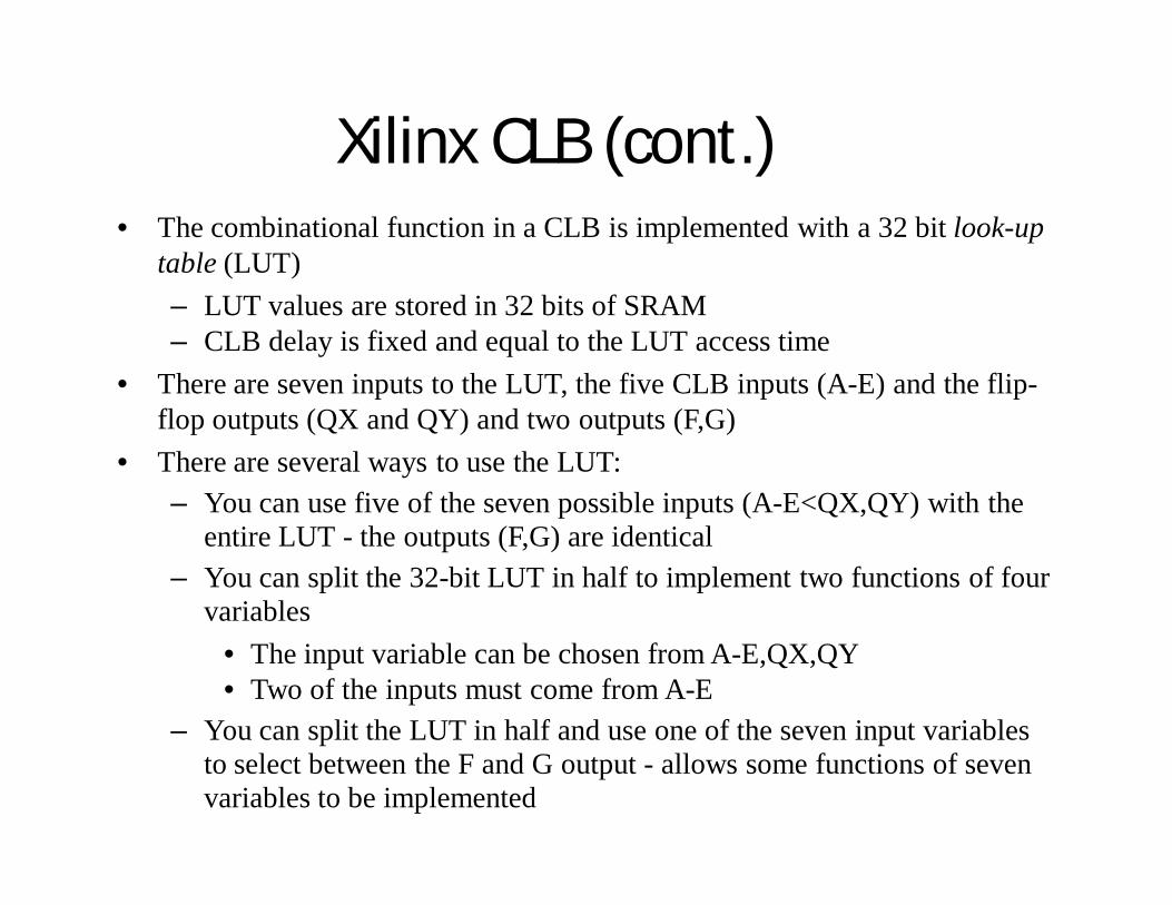
Xilinx CLB (cont.)• The combinational function in a CLB is implemented with a 32 bit look-up
table (LUT)– LUT values are stored in 32 bits of SRAM– CLB delay is fixed and equal to the LUT access time
• There are seven inputs to the LUT, the five CLB inputs (A-E) and the flip-flop outputs (QX and QY) and two outputs (F,G)
• There are several ways to use the LUT:– You can use five of the seven possible inputs (A-E<QX,QY) with the
entire LUT - the outputs (F,G) are identical– You can split the 32-bit LUT in half to implement two functions of four
variables• The input variable can be chosen from A-E,QX,QY• Two of the inputs must come from A-E
– You can split the LUT in half and use one of the seven input variables to select between the F and G output - allows some functions of seven variables to be implemented
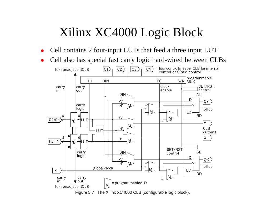
Xilinx XC4000 Logic Block Cell contains 2 four-input LUTs that feed a three input LUT Cell also has special fast carry logic hard-wired between CLBs
Figure 5.7 The Xilinx XC4000 CLB (configurable logic block).
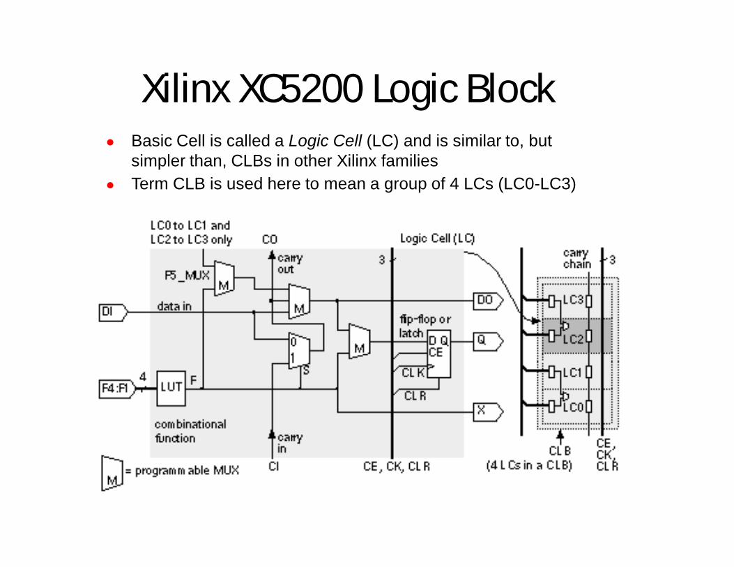
Xilinx XC5200 Logic Block Basic Cell is called a Logic Cell (LC) and is similar to, but
simpler than, CLBs in other Xilinx families Term CLB is used here to mean a group of 4 LCs (LC0-LC3)
Implementing Functions with Xilinx CLBs
• Combinational logic functions all have the same delay - a 5 input NAND is as slow (fast) as an inverter
• For maximum efficiency, the tools must group logic functions into blocks the utilize the CLB efficiently (i.e., utilize an high percentage of its functionality)
• LUT simplifies the timing model when using synchronous logic
• The LUT matches the Xilinx SRAM programming technology well
• SRAM within the LUT can be used a general purpose, on-chip SRAM, but it is expensive
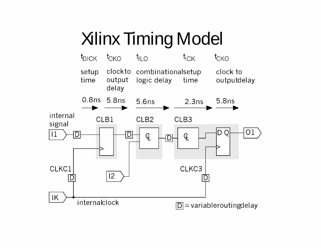
Xilinx Timing Model
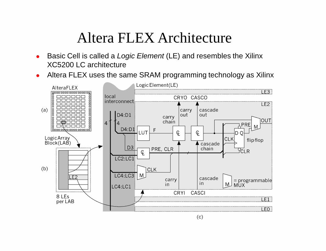
Altera FLEX Architecture Basic Cell is called a Logic Element (LE) and resembles the Xilinx
XC5200 LC architecture Altera FLEX uses the same SRAM programming technology as Xilinx
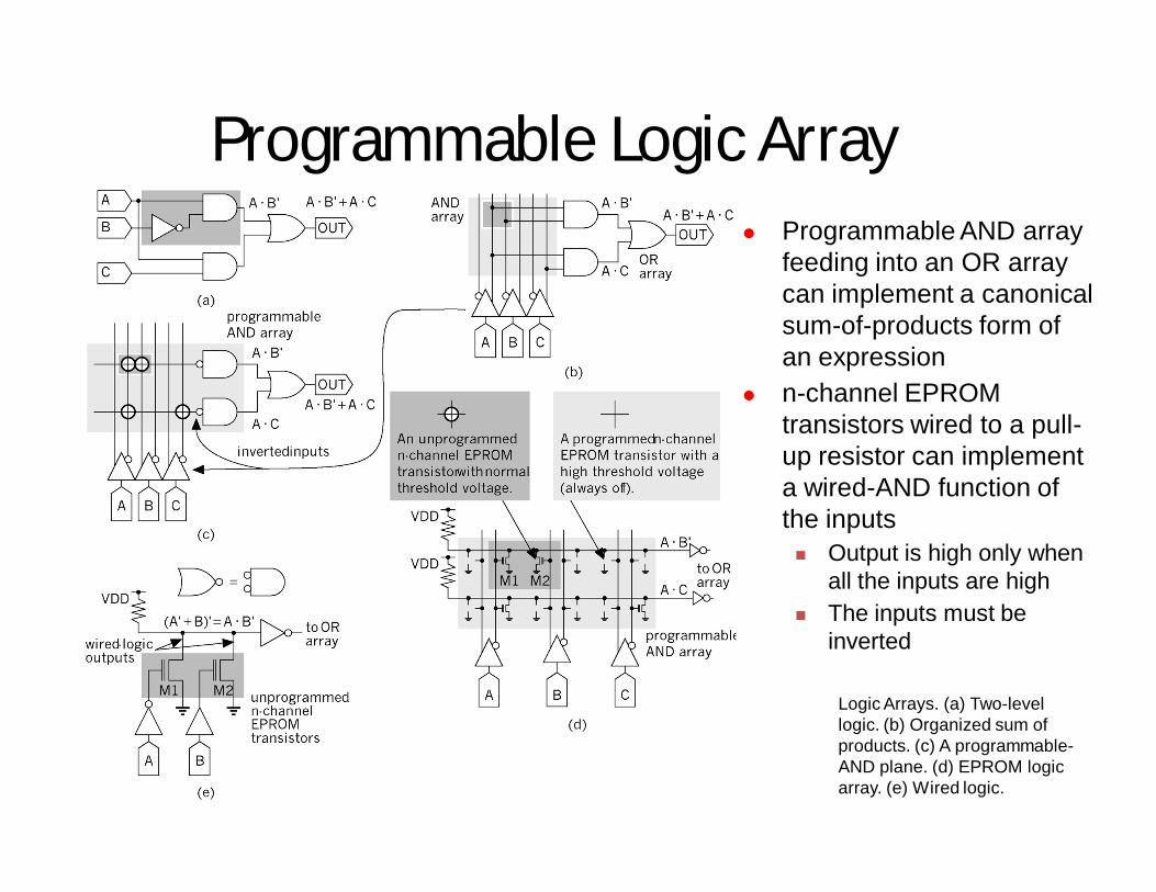
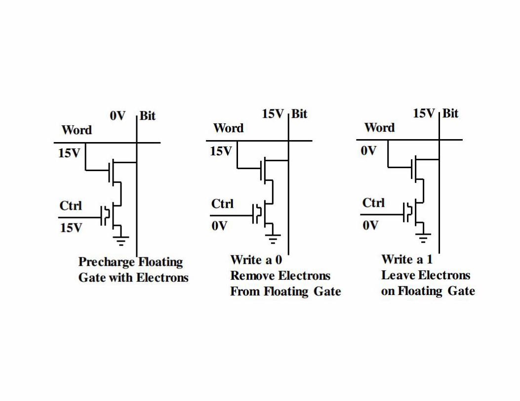
Programmable Logic Array Programmable AND array
feeding into an OR array can implement a canonical sum-of-products form of an expression
n-channel EPROM transistors wired to a pull-up resistor can implement a wired-AND function of the inputs Output is high only when
all the inputs are high The inputs must be
inverted
Logic Arrays. (a) Two-level logic. (b) Organized sum of products. (c) A programmable-AND plane. (d) EPROM logic array. (e) Wired logic.
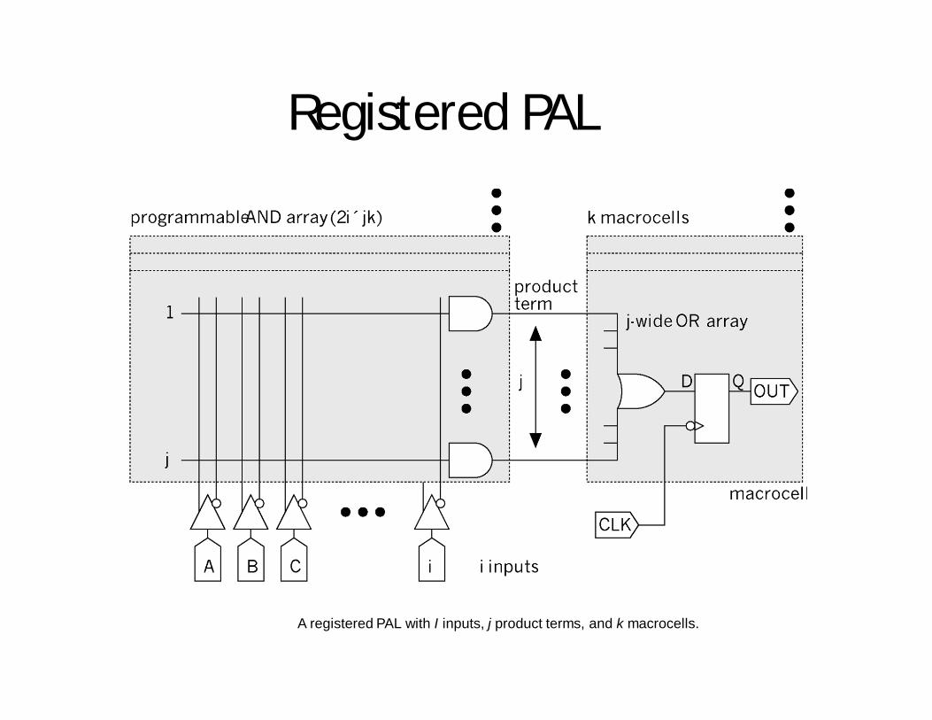
Registered PAL
A registered PAL with I inputs, j product terms, and k macrocells.
Logic Expander
• A logic expander is an output line of the AND array that feeds back as an input to the array itself
• Logic expanders can help implement functions that require more product terms than are available in a simple PAL
• Consider implementing this function in in a three-wide OR array:
F = A’ · C · D + B’ · C · D + A · B + B · C’• This can be rewritten as a “sum of (products of products):
F = (A’ + B’) · C · D + (A + C’) · BF = (A · B)’ (C · D) + (A’ · C)’ · B
• Logic expanders can be used to form the expander terms (A · B)’ and (A’ · C)’
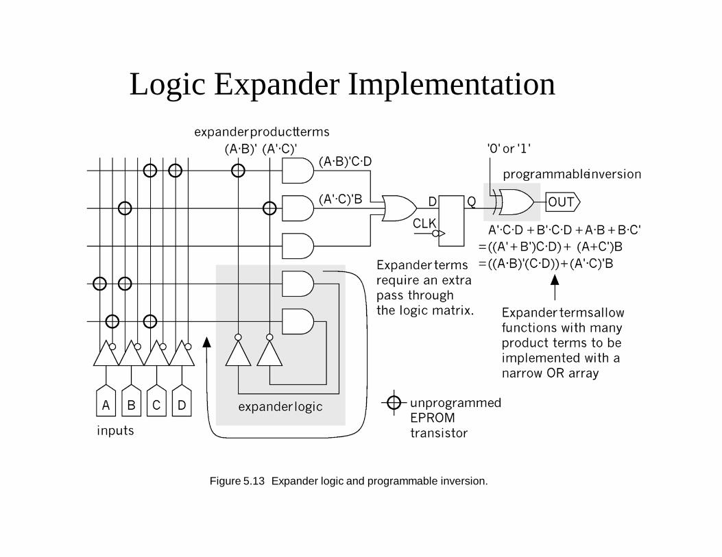
Logic Expander Implementation
Figure 5.13 Expander logic and programmable inversion.
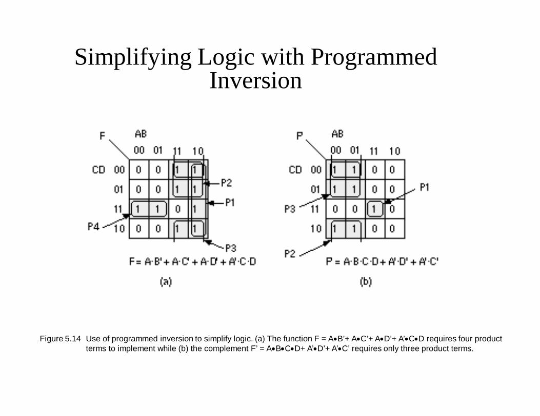
Simplifying Logic with Programmed Inversion
Figure 5.14 Use of programmed inversion to simplify logic. (a) The function F = AB’+ AC’+ AD’+ A’CD requires four product terms to implement while (b) the complement F’ = ABCD+ A’D’+ A’C’ requires only three product terms.
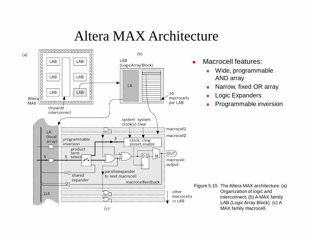
Altera MAX Architecture
Macrocell features: Wide, programmable
AND array Narrow, fixed OR array Logic Expanders Programmable inversion
Figure 5.15 The Altera MAX architecture. (a) Organization of logic and interconnect. (b) A MAX family LAB (Logic Array Block). (c) A MAX family macrocell.
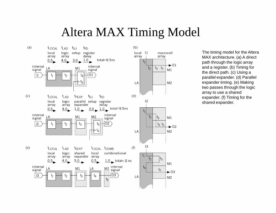
Altera MAX Timing ModelThe timing model for the AlteraMAX architecture. (a) A direct path through the logic array and a register. (b) Timing for the direct path. (c) Using a parallel expander. (d) Parallel expander timing. (e) Making two passes through the logic array to use a shared expander. (f) Timing for the shared expander.
UNIT III
PROGRAMMABLE ASIC INTERCONNECT,
PROGRAMMABLE ASIC DESIGN SOFTWARE AND LOW LEVEL
DESIGN
Actel ACT• The Actel ACT family interconnect scheme shown which is
similar to a channeled gate array. The channel routing uses dedicated rectangular areas of fixed size within the chip called wiring channels (or just channels ).
• The horizontal channels run across the chip in the horizontal direction. In the vertical direction there are similar vertical channels that run over the top of the basic logic cells, the Logic Modules.
• Within the horizontal or vertical channels wires run horizontally or vertically, respectively, within tracks .
• Each track holds one wire. The capacity of a fixed wiring channel is equal to the number of tracks it contains.
• A detailed view of the channel and the connections to each Logic Module—the input stubs and output stubs are shown.
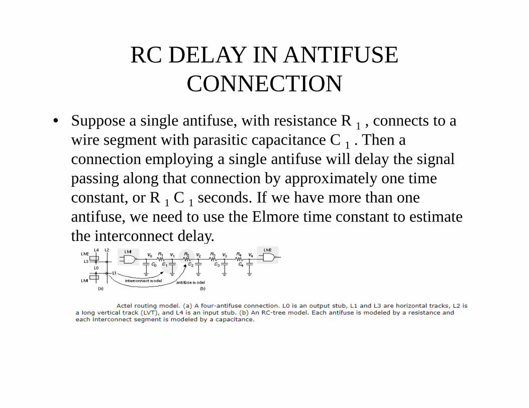
RC DELAY IN ANTIFUSE CONNECTION
• Suppose a single antifuse, with resistance R 1 , connects to a wire segment with parasitic capacitance C 1 . Then a connection employing a single antifuse will delay the signal passing along that connection by approximately one time constant, or R 1 C 1 seconds. If we have more than one antifuse, we need to use the Elmore time constant to estimate the interconnect delay.
RC Delay calculation
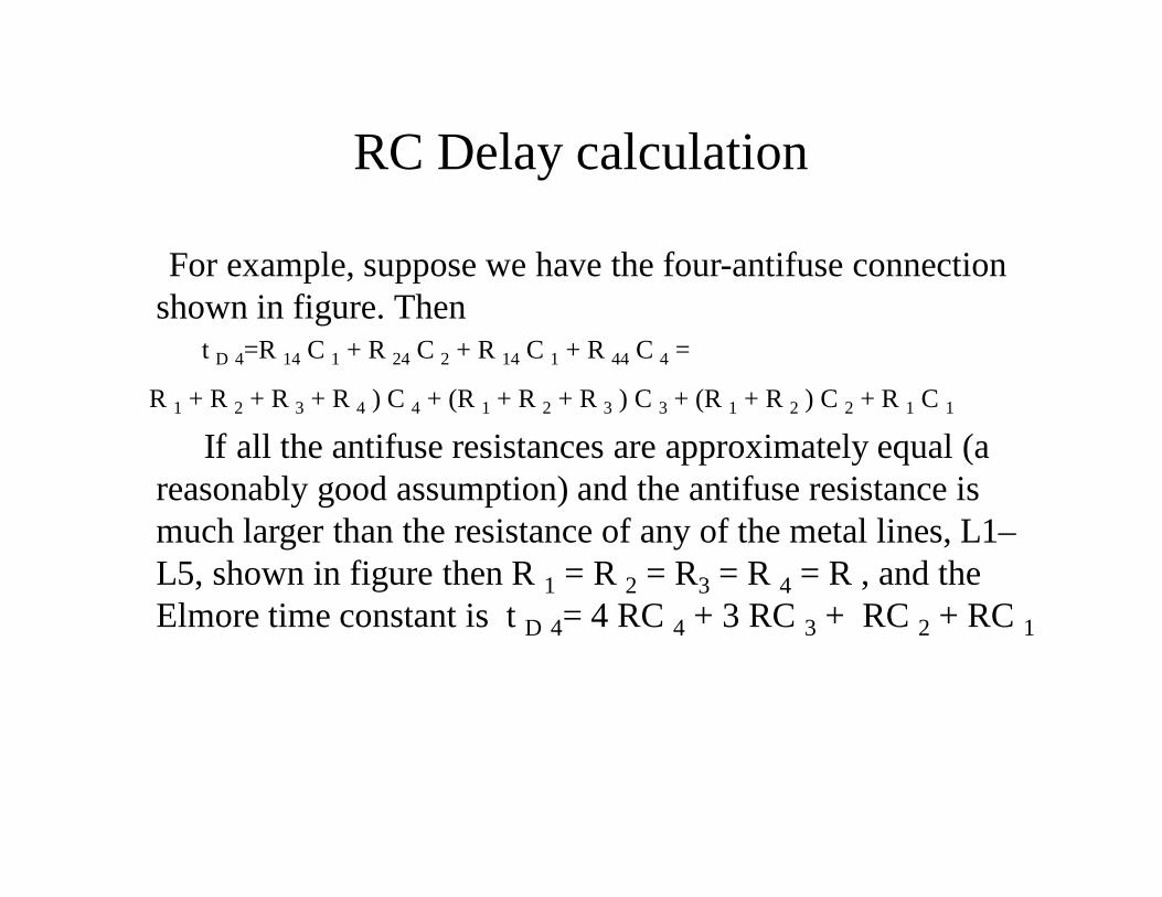
For example, suppose we have the four-antifuse connection shown in figure. Then
t D 4=R 14 C 1 + R 24 C 2 + R 14 C 1 + R 44 C 4 =
R 1 + R 2 + R 3 + R 4 ) C 4 + (R 1 + R 2 + R 3 ) C 3 + (R 1 + R 2 ) C 2 + R 1 C 1
If all the antifuse resistances are approximately equal (a reasonably good assumption) and the antifuse resistance is much larger than the resistance of any of the metal lines, L1–L5, shown in figure then R 1 = R 2 = R3 = R 4 = R , and the Elmore time constant is t D 4= 4 RC 4 + 3 RC 3 + RC 2 + RC 1
ACT 2 and ACT 3 INTERCONNECT
• The ACT 1 architecture uses two antifuses for routing nearby modules, three antifuses to join horizontal segments, and four antifuses to use a horizontal or vertical long track.
• The ACT 2 and ACT 3 architectures use increased interconnect resources over the ACT 1 device that we have described. This reduces further the number of connections that need more than two antifuses. Delay is also reduced by decreasing the population of antifuses in the channels, and by decreasing the antifuse resistance of certain critical antifuses (by increasing the programming current).
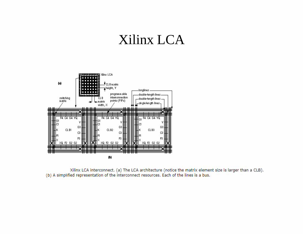
Xilinx LCA
Xilinx LCA Interconnect Architecture
• The vertical lines and horizontal lines run between CLBs.• The general-purpose interconnect joins switch boxes (also
known as magic boxes or switching matrices).• The long lines run across the entire chip. It is possible to form
internal buses using long lines and the three-state buffers that are next to each CLB.
• The direct connections (not used on the XC4000) bypass the switch matrices and directly connect adjacent CLBs.
• The Programmable Interconnection Points ( PIP s) are programmable pass transistors that connect the CLB inputs and outputs to the routing network.
• The bidirectional ( BIDI ) interconnect buffers restore the logic level and logic strength on long interconnect paths.
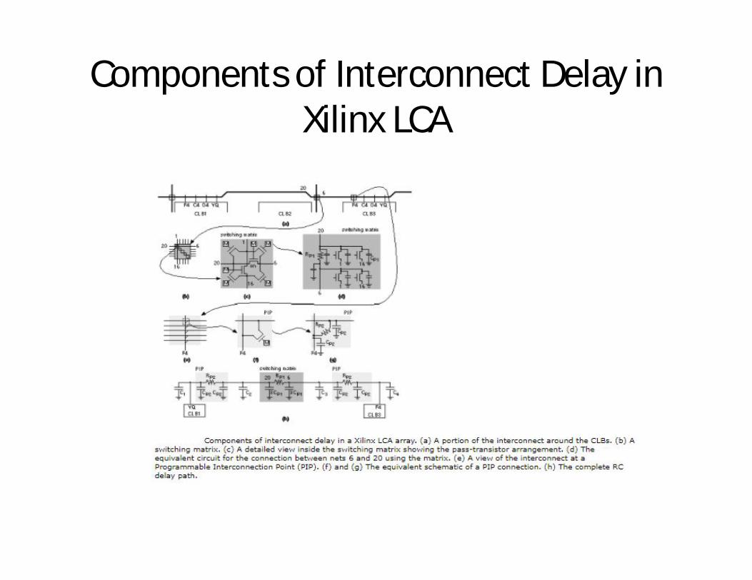
Components of Interconnect Delay in Xilinx LCA
cont…
• C1 = 3CP1 + 3CP2 + 0. 5C LX is the parasitic capacitance due to the switch matrix and PIPs (F4, C4, G4) for CLB1, and half of the line capacitance for the double-length line adjacent to CLB1.
• C P1 and R P1 are the switching-matrix parasitic capacitance and resistance.
• C P2 and R P2 are the parasitic capacitance and resistance for the PIP connecting YQ of CLB1 and F4 of CLB3.
• C2 = 0. 5CLX + CLX accounts for half of the line adjacent to CLB1 and the line adjacent to CLB2.
• C 3 = 0. 5C LX accounts for half of the line adjacent to CLB3.• C 4 = 0. 5C LX + 3C P2 + C LX + 3C P1 accounts for half of the line
adjacent to CLB3, the PIPs of CLB3 (C4, G4, YQ), and the rest of the line and switch matrix capacitance following CLB3.
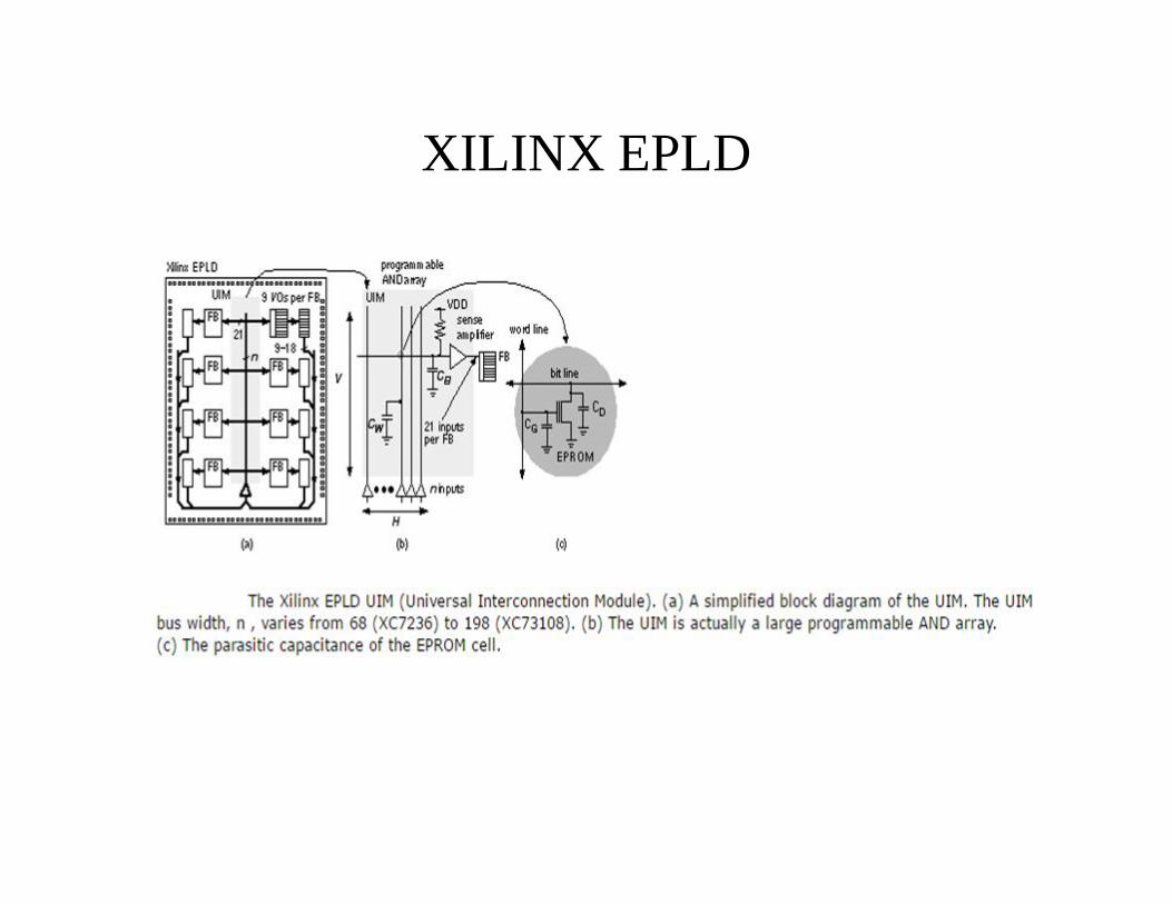
XILINX EPLD
XILINX EPLD• The Xilinx EPLD family uses an interconnect bus known as Universal
Interconnection Module ( UIM ) to distribute signals within the FPGA. The UIM, is a programmable AND array with constant delay from any input to any output.
C G is the fixed gate capacitance of the EPROM device.C D is the fixed drain parasitic capacitance of the EPROM device.C B is the variable horizontal bus (“bit” line) capacitance.C W is the variable vertical bus (“word” line) capacitance.
• The UIM has 21 output connections to each FB. Most (but not all) of the nine I/O cells attached to each FB have two input connections to the UIM, one from a chip input and one feedback from the macrocell output. For example, the XC7272 has 18 I/O cells that are outputs only and thus have only one connection to the UIM,
• In the UIM: the XC7272, for example, has H = 126 tracks and V = 168/2 = 84 tracks. The actual physical height, V , of the UIM is determined by the size of the FBs, and is close to the die height.
Altera MAX 5000 and 7000
• Altera MAX 5000 devices (except the EPM5032, which has only one LAB) and all MAX 7000 devices use a Programmable Interconnect Array ( PIA )
• The PIA is a cross-point switch for logic signals traveling between LABs. The advantages of this architecture (which uses a fixed number of connections) over programmable interconnection schemes (which use a variable number of connections) is the fixed routing delay.
• An additional benefit of the simpler nature of a large regular interconnect structure is the simplification and improved speed of the placement and routing software.
Altera MAX 5000 and 7000
A simplified block diagram of the Altera MAX interconnect scheme. (a) The PIA (Programmable Interconnect Array) is deterministic—delay is independent of the path length. (b) Each LAB (Logic Array Block) contains a programmable AND array. (c) Interconnect timing within a LAB is also fixed.
Altera Max 9000
• The size of the MAX 9000 LAB arrays varies between 4 * 5 (rows, columns) for the EPM9320 and 7*5 for the EPM9560. The MAX 9000 is an extremely coarse-grained architecture, typical of complex PLDs, but the LABs themselves have a finer structure.
• Sometimes we say that complex PLDs with arrays (LABs in the Altera MAX family) that are themselves arrays (of macrocells) have a dual-grain architecture .The Altera MAX 9000 interconnect scheme. (a) A 4 *5 array of Logic Array Blocks (LABs), the same size
as the EMP9400 chip. (b) A simplified block diagram of the interconnect architecture showing the connection of the FastTrack buses to a LAB.
Altera Flex
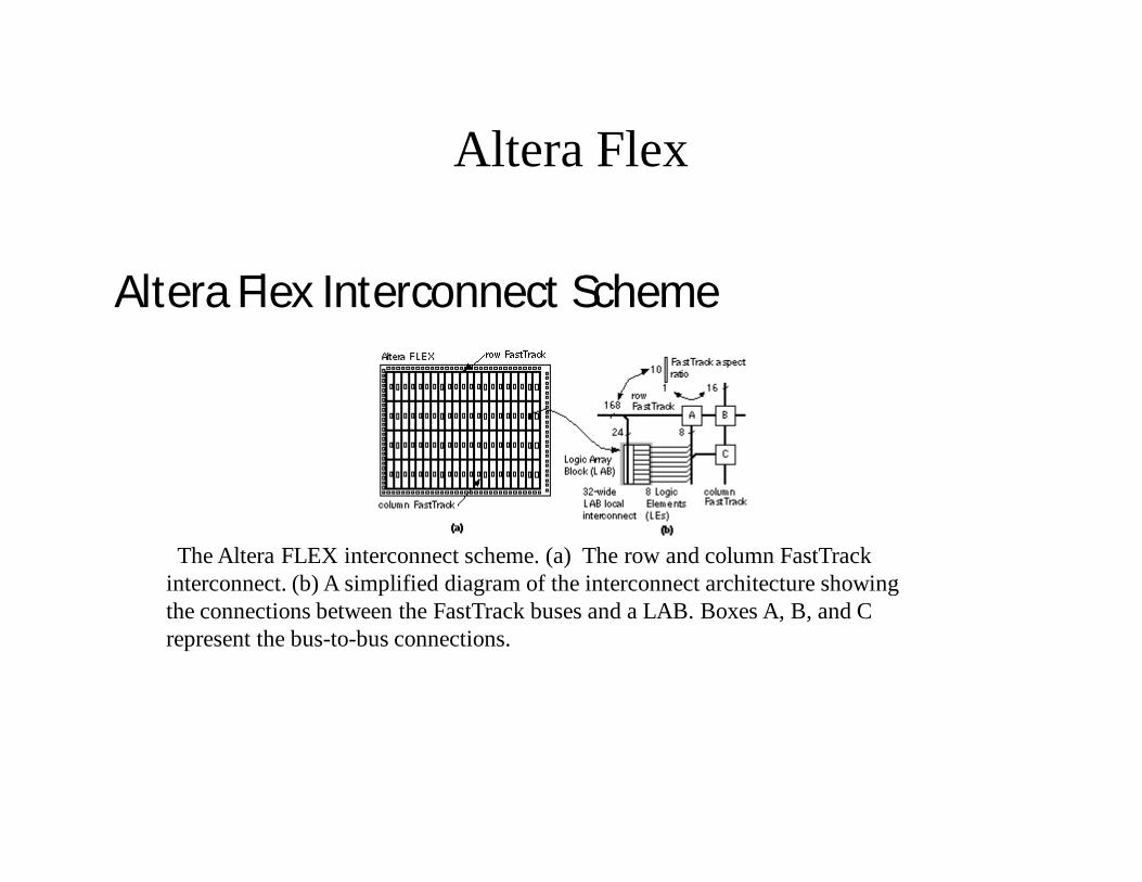
Altera Flex Interconnect Scheme
The Altera FLEX interconnect scheme. (a) The row and column FastTrackinterconnect. (b) A simplified diagram of the interconnect architecture showing the connections between the FastTrack buses and a LAB. Boxes A, B, and C represent the bus-to-bus connections.
Altera Flex• Altera refers to the FLEX interconnect and MAX 9000
interconnect by the same name, FastTrack, but the two are different because the granularity of the logic cell arrays is different.
• The FLEX architecture is of finer grain than the MAX arrays—because of the difference in programming technology. The FLEX horizontal interconnect is much denser (at 168 channels per row) than the vertical interconnect (16 channels per column), creating an aspect ratio for the interconnect of over 10:1 (168:16).
• This imbalance is partly due to the aspect ratio of the die, the array, and the aspect ratio of the basic logic cell, the LAB.
LOW LEVEL PROGRAMMING LANGUAGES
• ABEL is a PLD programming language from Data I/O.• CUPL is a PLD design language from Logical Devices.• PALASM is a PLD design language from AMD/MMI.
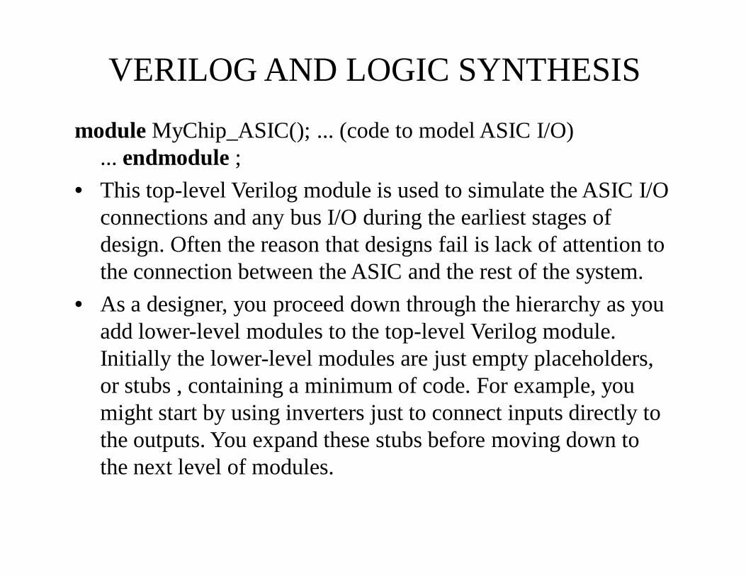
module MyChip_ASIC(); ... (code to model ASIC I/O) ... endmodule ;
• This top-level Verilog module is used to simulate the ASIC I/O connections and any bus I/O during the earliest stages of design. Often the reason that designs fail is lack of attention to the connection between the ASIC and the rest of the system.
• As a designer, you proceed down through the hierarchy as you add lower-level modules to the top-level Verilog module. Initially the lower-level modules are just empty placeholders, or stubs , containing a minimum of code. For example, you might start by using inverters just to connect inputs directly to the outputs. You expand these stubs before moving down to the next level of modules.
VERILOG AND LOGIC SYNTHESIS
VERILOG AND LOGIC SYNTHESIS
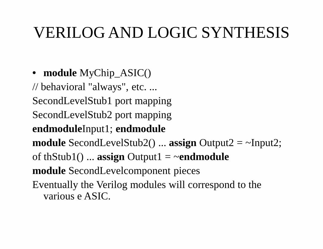
• module MyChip_ASIC()// behavioral "always", etc. ...SecondLevelStub1 port mappingSecondLevelStub2 port mappingendmoduleInput1; endmodulemodule SecondLevelStub2() ... assign Output2 = ~Input2;of thStub1() ... assign Output1 = ~endmodulemodule SecondLevelcomponent pieces Eventually the Verilog modules will correspond to the
various e ASIC.
VHDL and Logic Synthesis• Most logic synthesizers insist we follow a set of rules when we use a
logic system to ensure that what we synthesize matches the behavioral description. Here is a typical set of rules for use with the IEEE VHDL nine-value system:
• logic values corresponding to states '1' , 'H' , '0' , and 'L' in any manner Can be used.
• Some synthesis tools do not accept the uninitialized logic state 'U' .• You can use logic states 'Z' , 'X' , 'W' , and '-' in signal and variable
assignments in any manner. 'Z' is synthesized to three-state logic.• The states 'X' , 'W' , and '-' are treated as unknown or don’t care values.• The values 'Z' , 'X' , 'W' , and '-' may be used in conditional clauses such
as the comparison in an if or case statement. However, some synthesis tools will ignore them and only match surrounding '1' and '0' bits. Consequently, a synthesized design may behave differently from the simulation if a stimulus uses 'Z' , 'X' , 'W' or '-' . The IEEE synthesis packages provide the STD_MATCH function for comparisons.
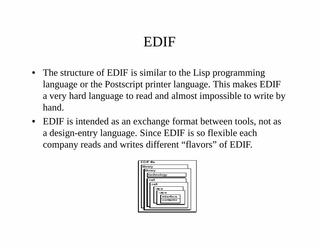
EDIF
• The structure of EDIF is similar to the Lisp programming language or the Postscript printer language. This makes EDIF a very hard language to read and almost impossible to write by hand.
• EDIF is intended as an exchange format between tools, not as a design-entry language. Since EDIF is so flexible each company reads and writes different “flavors” of EDIF.
EDIF
• Within an EDIF file are one or more libraries of cell descriptions. Each library contains technology information that is used in describing the characteristics of the cells it contains. Each cell description contains one or more user-named views of the cell.
• Each view is defined as a particular view Type and contains an interface description that identifies where the cell may be connected to and, possibly, a contents description that identifies the components and related interconnections that make up the cell.
• The semantics of EDIF are defined by the EDIF keywords . Keywords are the only types of name that can immediately follow a left parenthesis.
EDIF
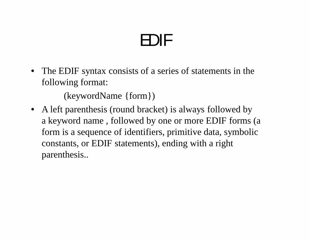
• The EDIF syntax consists of a series of statements in the following format:
(keywordName {form})• A left parenthesis (round bracket) is always followed by
a keyword name , followed by one or more EDIF forms (a form is a sequence of identifiers, primitive data, symbolic constants, or EDIF statements), ending with a right parenthesis..
CFI Design Representation• The CAD Framework Initiative ( CFI ) is an independent nonprofit
organization working on the creation of standards for the electronic CAD industry. One of the areas in which CFI is working is the definition of standards for design representation ( DR ). The CFI 1.0 standard [ CFI, 1992] has tackled the problems of ambiguity in the area of definitions and terms for schematics by defining an information model ( IM ) for electrical connectivity information.
• It helps to solidify the concepts of the terms and definitions such as cell, net, and instance that we have already discussed. However, there are additional new concepts and terms to define in order to present the standard model, so this is not a good way to introduce schematic terminology.
• The ASIC design engineer is becoming more of a programmer and less of a circuit designer. This trend shows no sign of stopping as ASICs grow larger and systems more complex. A precise understanding of how tools operate and interact is becoming increasingly important
CFI CONNECTIVITY MODEL
UNIT IV
SILICON ON CHIP DESIGN
System On Chip• An System on Chip (SoC) is an integrated circuit that
implements most or all of the function of a complete electronic system
• Four vital areas of SoC:
Higher levels of abstraction
IP and platform re-use
IP creation – ASIPs, interconnect and algorithm
Earlier software development and integration
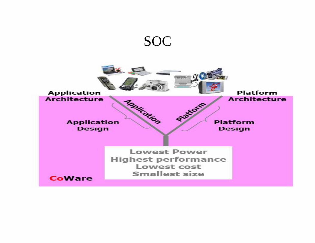
SOC
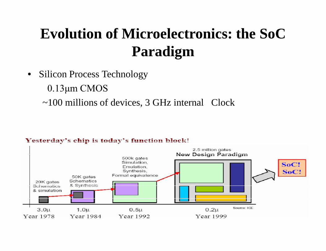
Evolution of Microelectronics: the SoCParadigm
• Silicon Process Technology0.13μm CMOS
~100 millions of devices, 3 GHz internal Clock
• n of Microelectronics: the
Migration from ASICs to SoCs
• ASICs are logic chips designed by end customers to perform a specific function for a desired application.
• ASIC vendors supply libraries for each technology they provide. In most cases, these libraries contain predesigned and preverified logic circuits.
• ASIC technologies are:
gate array
standard cell
full custom
Migration from ASICs to SoCs
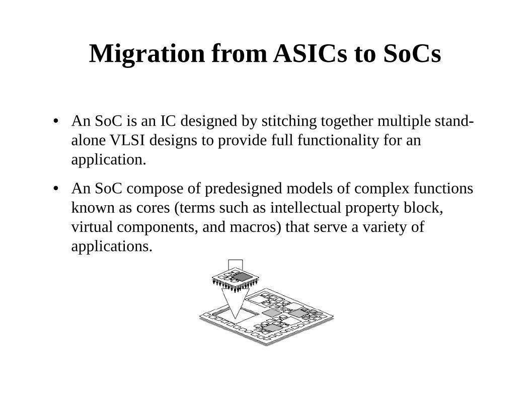
• An SoC is an IC designed by stitching together multiple stand-alone VLSI designs to provide full functionality for an application.
• An SoC compose of predesigned models of complex functions known as cores (terms such as intellectual property block, virtual components, and macros) that serve a variety of applications.
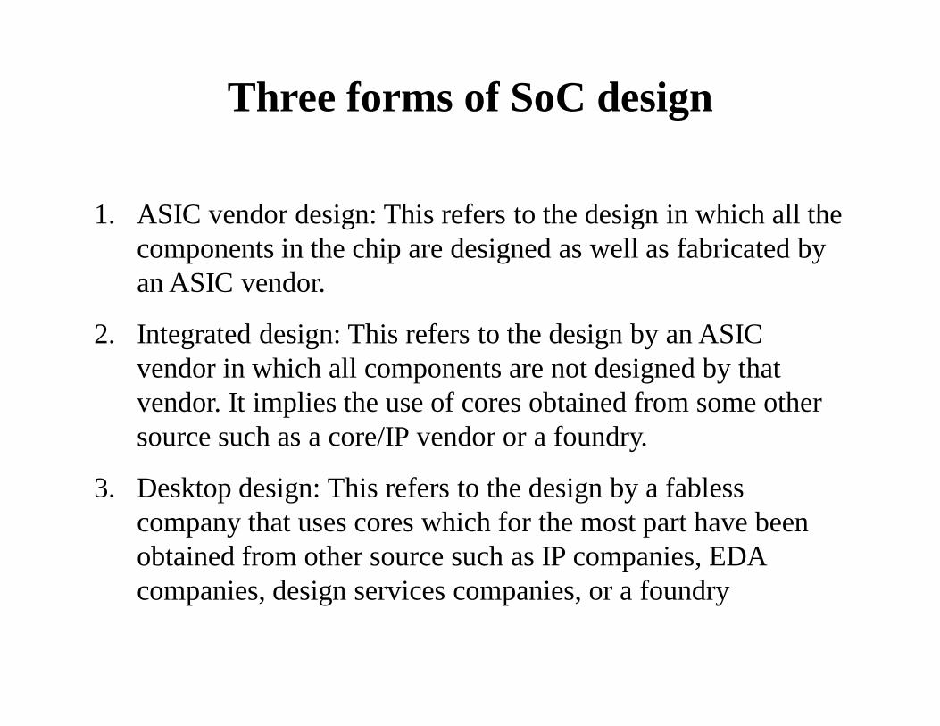
Three forms of SoC design
1. ASIC vendor design: This refers to the design in which all the components in the chip are designed as well as fabricated by an ASIC vendor.
2. Integrated design: This refers to the design by an ASIC vendor in which all components are not designed by that vendor. It implies the use of cores obtained from some other source such as a core/IP vendor or a foundry.
3. Desktop design: This refers to the design by a fabless company that uses cores which for the most part have been obtained from other source such as IP companies, EDA companies, design services companies, or a foundry
SoC Design Challenges
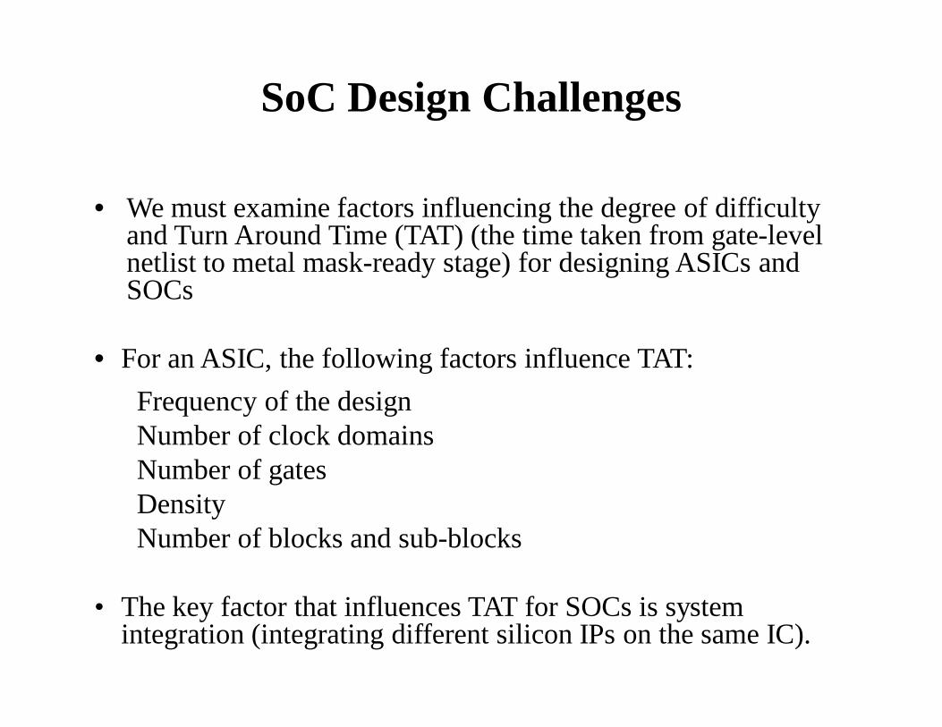
• We must examine factors influencing the degree of difficulty and Turn Around Time (TAT) (the time taken from gate-level netlist to metal mask-ready stage) for designing ASICs and SOCs
• For an ASIC, the following factors influence TAT:Frequency of the designNumber of clock domainsNumber of gatesDensityNumber of blocks and sub-blocks
• The key factor that influences TAT for SOCs is system integration (integrating different silicon IPs on the same IC).
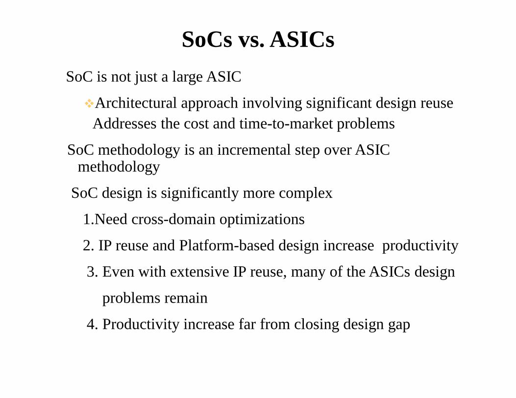
SoCs vs. ASICsSoC is not just a large ASIC
Architectural approach involving significant design reuseAddresses the cost and time-to-market problems
SoC methodology is an incremental step over ASIC methodology
SoC design is significantly more complex
1.Need cross-domain optimizations
2. IP reuse and Platform-based design increase productivity
3. Even with extensive IP reuse, many of the ASICs design
problems remain
4. Productivity increase far from closing design gap
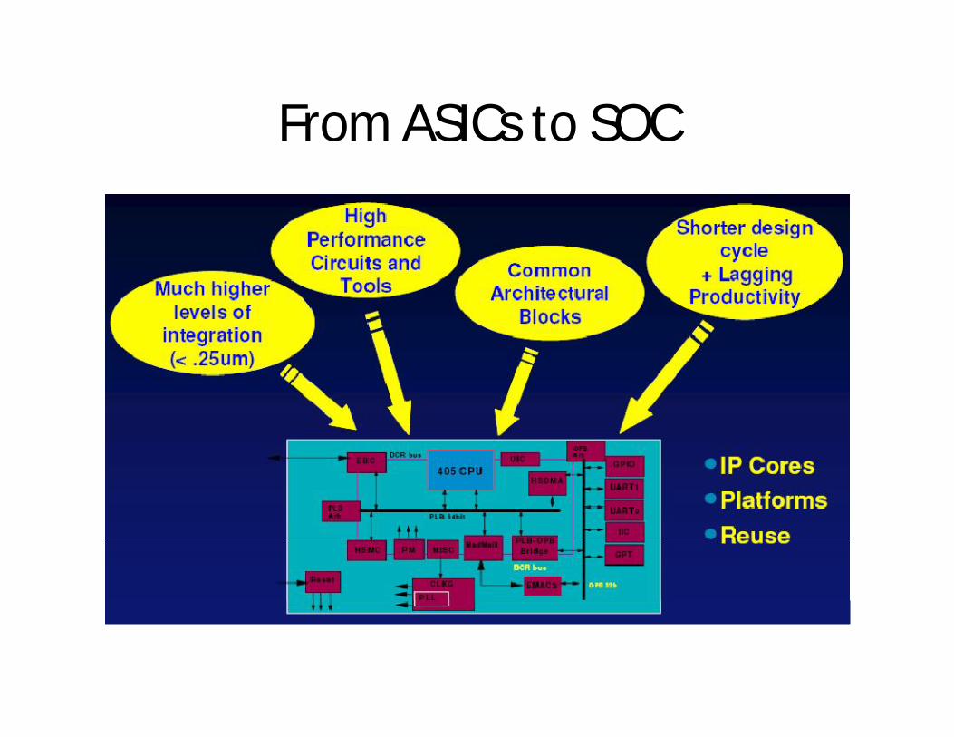
From ASICs to SOC
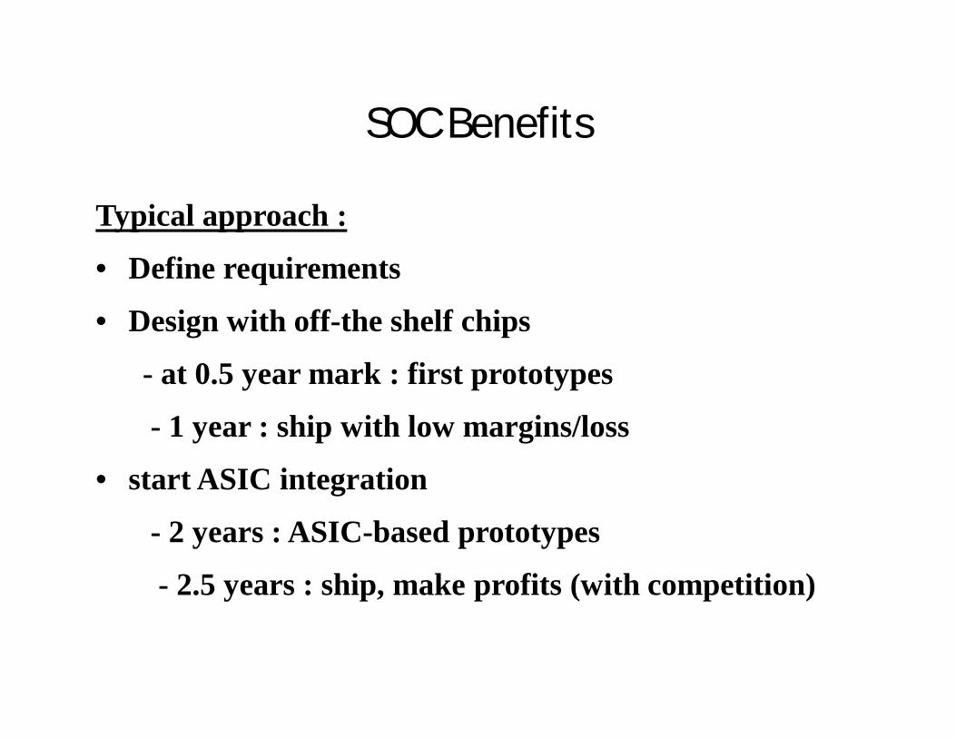
SOC Benefits
Typical approach :
• Define requirements
• Design with off-the shelf chips
- at 0.5 year mark : first prototypes
- 1 year : ship with low margins/loss
• start ASIC integration
- 2 years : ASIC-based prototypes
- 2.5 years : ship, make profits (with competition)
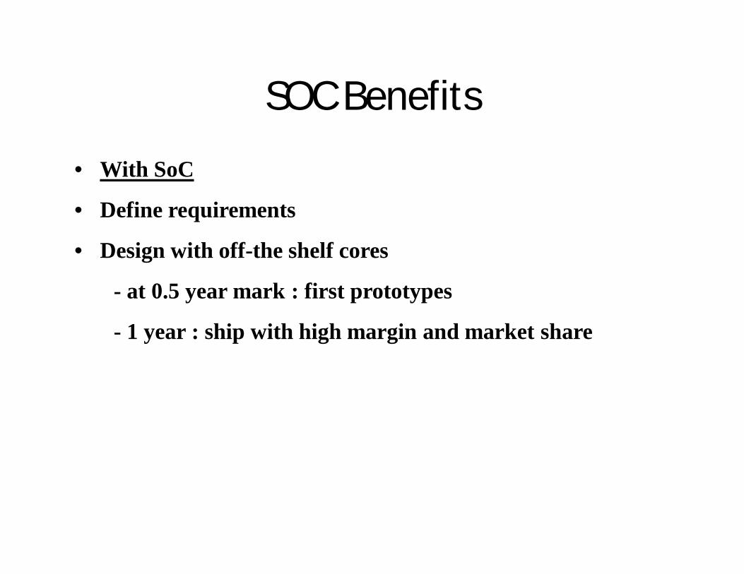
SOC Benefits
• With SoC
• Define requirements
• Design with off-the shelf cores
- at 0.5 year mark : first prototypes
- 1 year : ship with high margin and market share
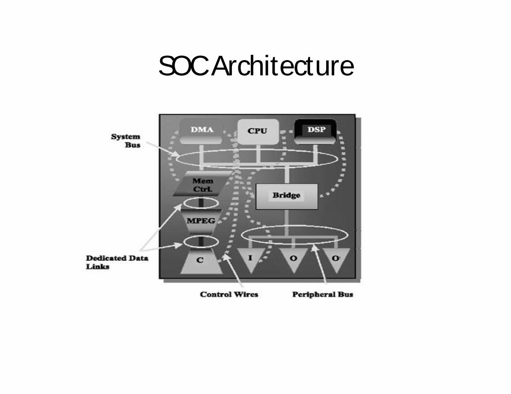
SOC Architecture
SOC ArchitectureA typical SoC consists of:• A microcontroller,microprocessor or digital signal processor core-
multiprocessor SoCs (MPSoC) having more than one processor core• memory blocks including a selection of ROM,RAM,EEPROM AND Flash
Memory.• timing sources including Oscillators and PLLs.• peripherals including Counter-timers, real-time timers and power -on reset
generators• external interfaces including industry standards such as
USB,Firewire,Ethernet.• analog interfaces including ADCs and DACs• A bus – either proprietary or industry-standard such as the AMBA bus
from ARM Holdings – connects these blocks. DMA controllers route data directly between external interfaces and memory, bypassing the processor core and thereby increasing the data throughput of the SoC.
VOICE OVER IP SOC
• A gateway VoIP SOC is a device used for functions such as Vocoders,echo cancellation,data/fax modems, and VoIP protocols.Currently there are number of these devices available from several vendors;typically these devices differ from each other by the type of functions and voice-processing algorithms they support.
VOICE OVER IP SOC
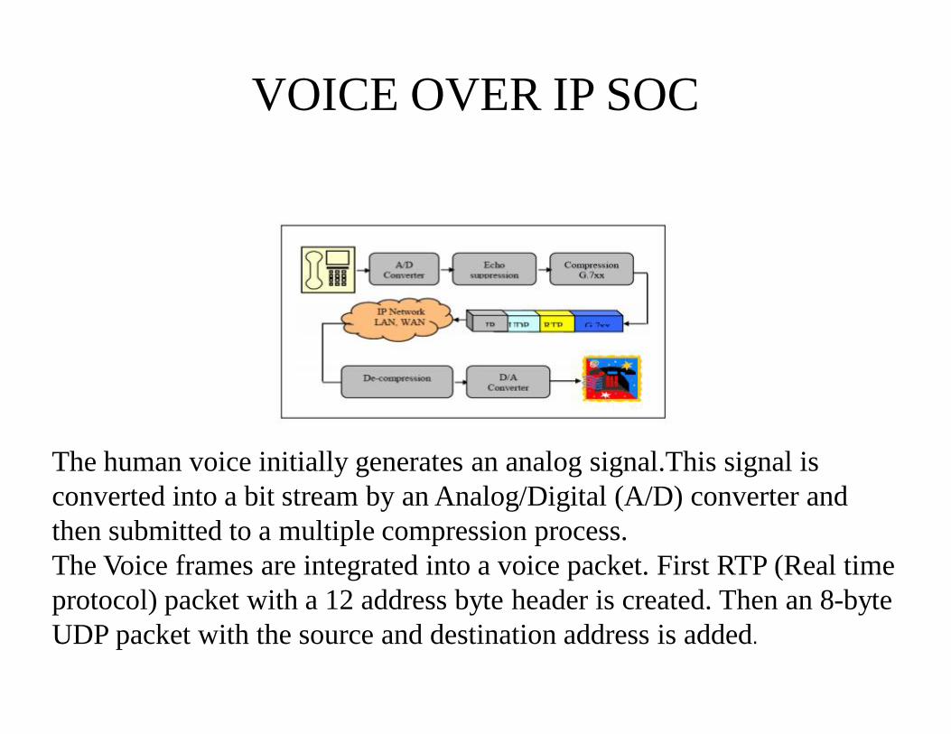
The human voice initially generates an analog signal.This signal is converted into a bit stream by an Analog/Digital (A/D) converter and then submitted to a multiple compression process. The Voice frames are integrated into a voice packet. First RTP (Real time protocol) packet with a 12 address byte header is created. Then an 8-byte UDP packet with the source and destination address is added.
VOICE OVER IP SOC
• Finally, a 20 byte IP header containing source and destination gateway IP address is added.The packet is sent through the internet where routers ands switches examine the destination address.
• When the destination receives the packet, the packet goes through the reverse process for playback.
• A minimal VoIP implementation requires two functionalities. First, it should be able to connect to other VoIP phones and, second, voice data should be carried by the Internet. The first requirement is fulfilled by using signaling. The second one is achieved by using speech coding algorithms.
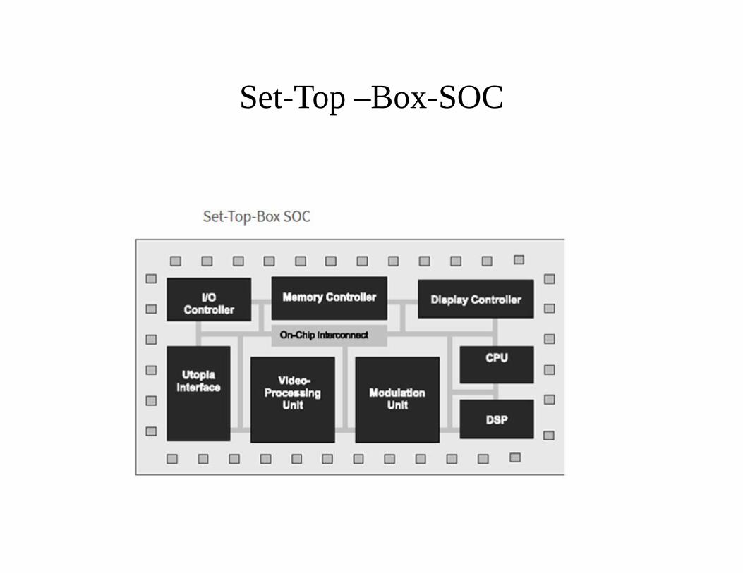
Set-Top –Box-SOC
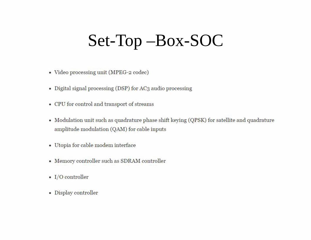
Set-Top –Box-SOC
INTELLECTUAL PROPERTY
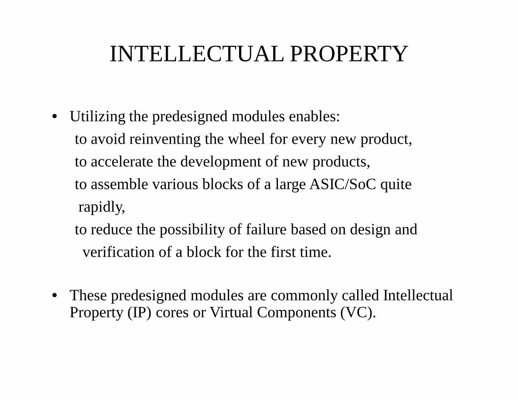
• Utilizing the predesigned modules enables: to avoid reinventing the wheel for every new product, to accelerate the development of new products, to assemble various blocks of a large ASIC/SoC quite rapidly,to reduce the possibility of failure based on design andverification of a block for the first time.
• These predesigned modules are commonly called Intellectual Property (IP) cores or Virtual Components (VC).
INTELLECTUAL PROPERTYCATEGORIES
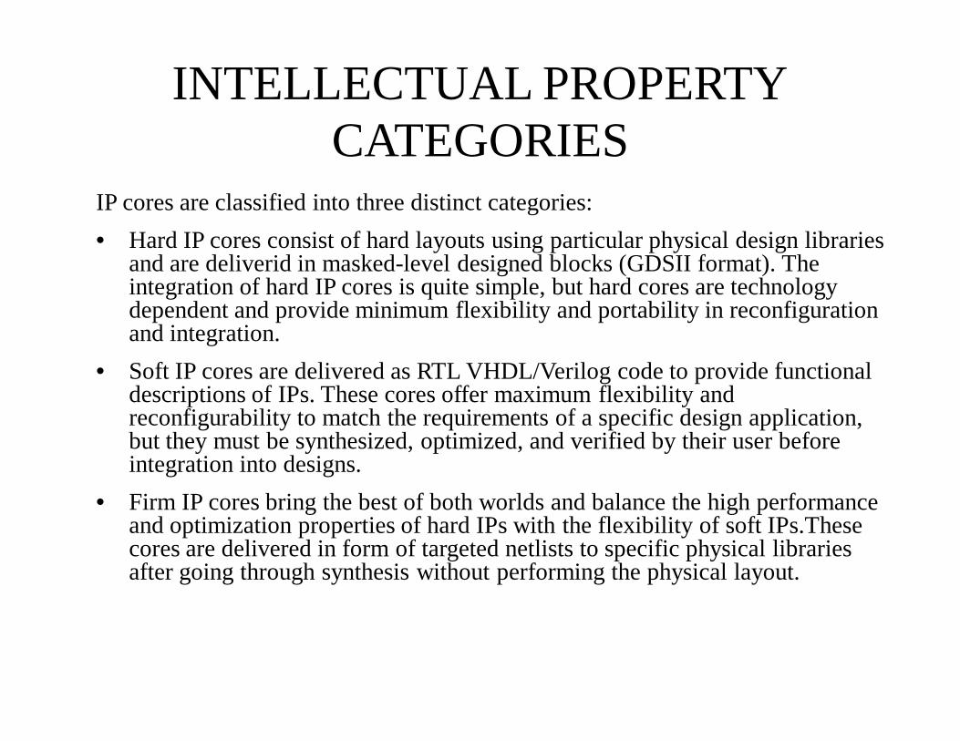
IP cores are classified into three distinct categories:• Hard IP cores consist of hard layouts using particular physical design libraries
and are deliverid in masked-level designed blocks (GDSII format). The integration of hard IP cores is quite simple, but hard cores are technology dependent and provide minimum flexibility and portability in reconfiguration and integration.
• Soft IP cores are delivered as RTL VHDL/Verilog code to provide functional descriptions of IPs. These cores offer maximum flexibility and reconfigurability to match the requirements of a specific design application, but they must be synthesized, optimized, and verified by their user before integration into designs.
• Firm IP cores bring the best of both worlds and balance the high performance and optimization properties of hard IPs with the flexibility of soft IPs.Thesecores are delivered in form of targeted netlists to specific physical libraries after going through synthesis without performing the physical layout.
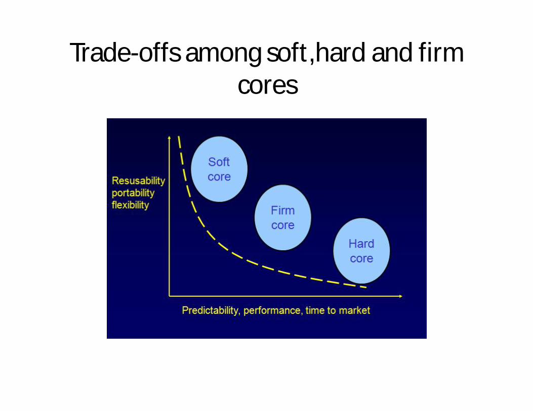
Trade-offs among soft,hard and firm cores
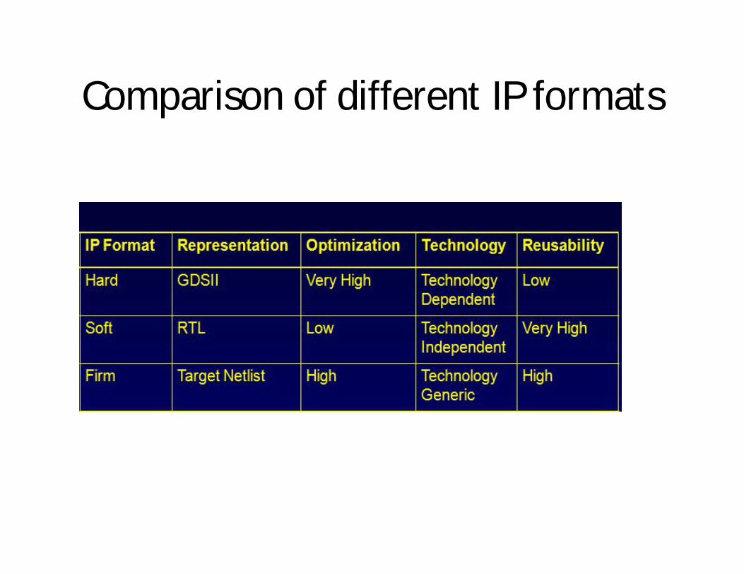
Comparison of different IP formats
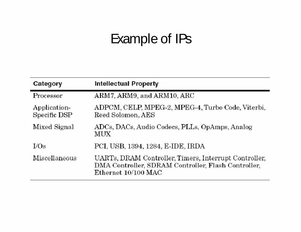
Example of IPs
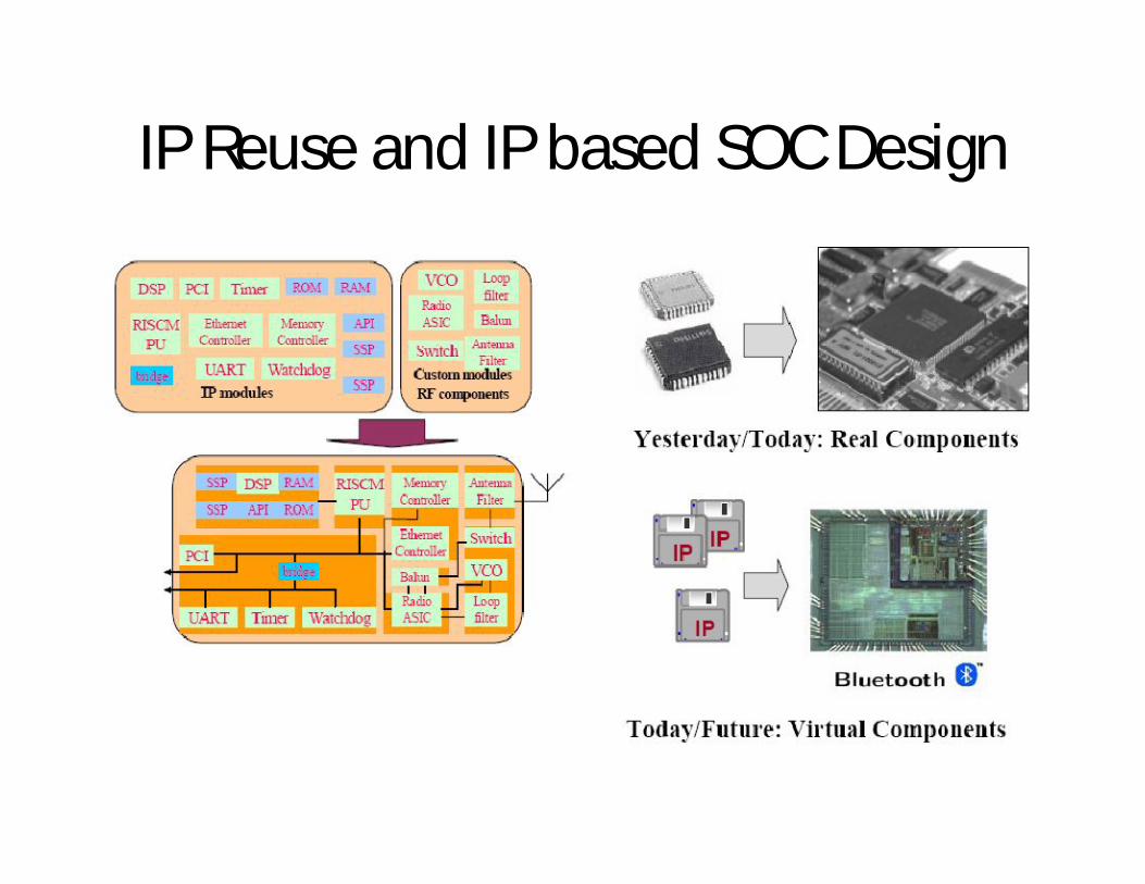
IP Reuse and IP based SOC Design
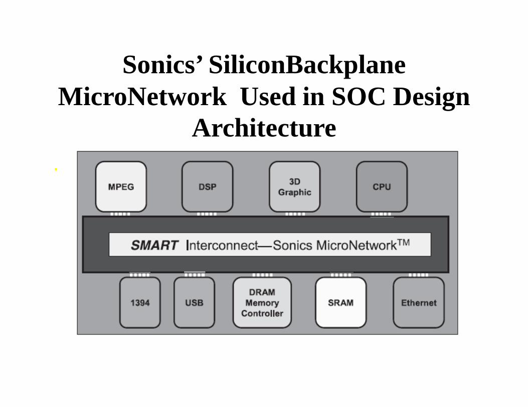
Sonics’ SiliconBackplaneMicroNetwork Used in SOC Design
Architecture.
Silicon BackPlane
• Silicon backplane uses a standard core interface known as the open protocol (OCP),Which delivers the first openly licensed, core centric protocol. The OCP defines a comprehensive, bus –independent, high performance, and configurable interface between IP cores and on-chip communication subsystems.OCP is a functional superset of Virtual socket Interface(VSI) Alliance virtual-component –interface(VCI) specification ,and enable SOC designers and semiconductor IP developers to prepare their cores for plug-and –play integration using Sonics’ Silicon Backplane.
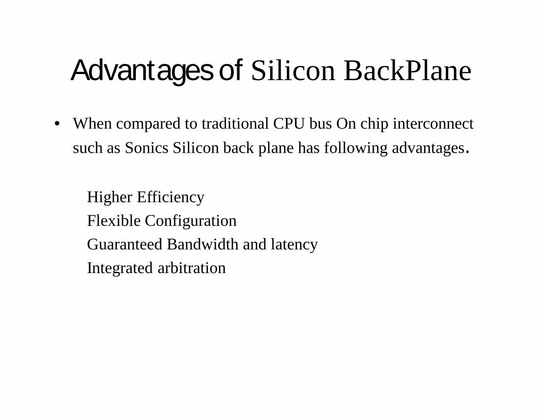
Advantages of Silicon BackPlane• When compared to traditional CPU bus On chip interconnect
such as Sonics Silicon back plane has following advantages.
Higher EfficiencyFlexible ConfigurationGuaranteed Bandwidth and latency Integrated arbitration

UNIT V
PHYSICAL AND LOW POWER DESIGN
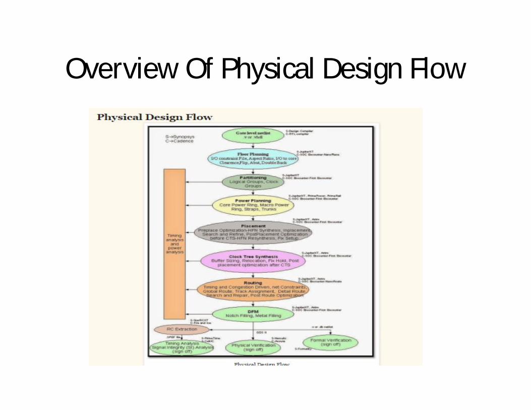
Overview Of Physical Design Flow
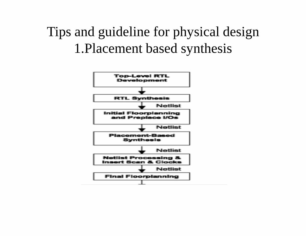
Tips and guideline for physical design1.Placement based synthesis
Placement Based Synthesis
• Placement is performed in four optimization phases:
1. Ire-placement optimization2. In placement optimization3. Post Placement Optimization (PPO) before clock tree synthesis (CTS)4. PPO after CTS.
Pre-placement Optimization optimizes the netlist before placement, HFNs are collapsed. It can also downsize the cells.
.
Placement Based Synthesis• In-placement optimization re-optimizes the logic based on
VR. This can perform cell sizing, cell moving, cell bypassing, net splitting, gate duplication, buffer insertion, area recovery. Optimization performs iteration of setup fixing, incremental timing and congestion driven placement.
Post placement optimization before CTS performs netlistoptimization with ideal clocks. It can fix setup, hold, max trans/cap violations. It can do placement optimization based on global routing. It re does HFN synthesis.
Post placement optimization after CTS optimizes timing with propagated clock. It tries to preserve clock skew
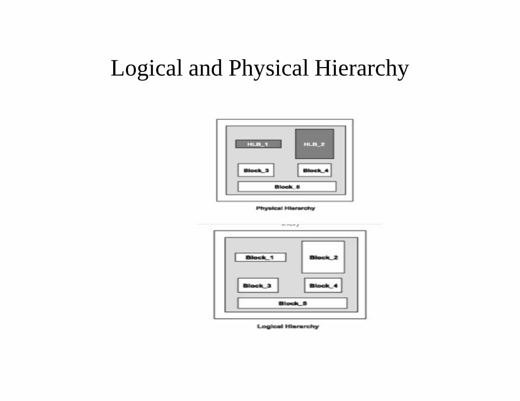
Logical and Physical Hierarchy
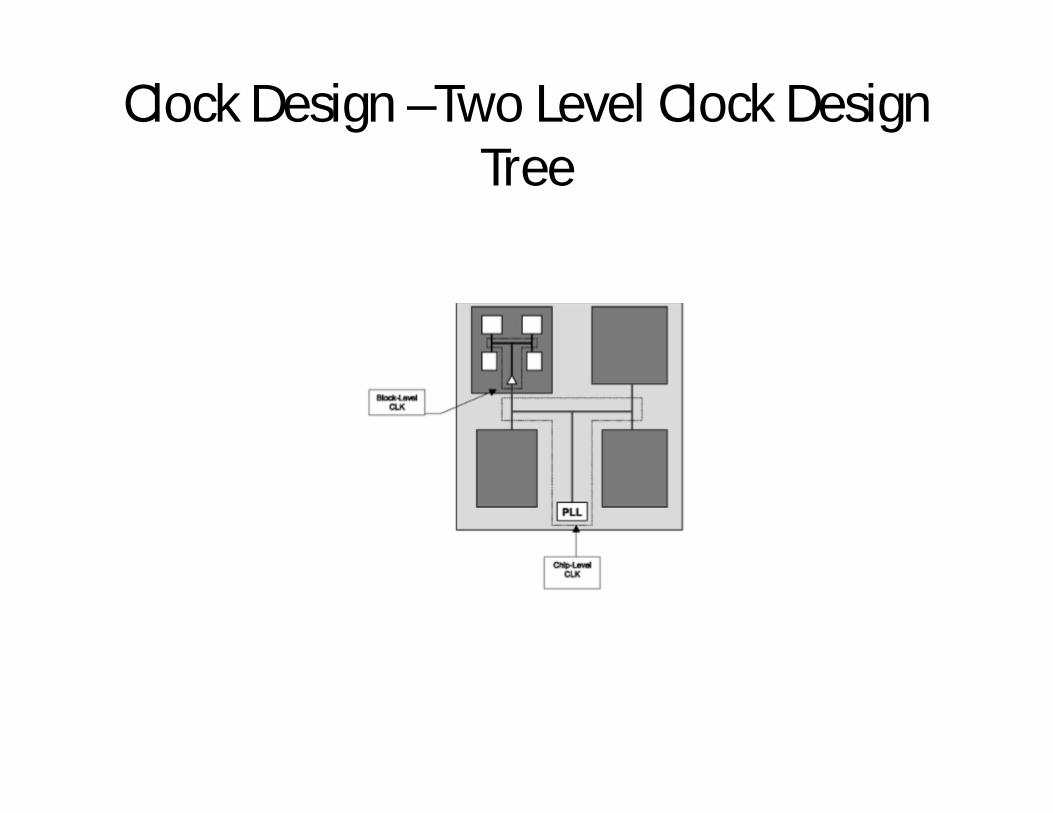
Clock Design –Two Level Clock Design Tree
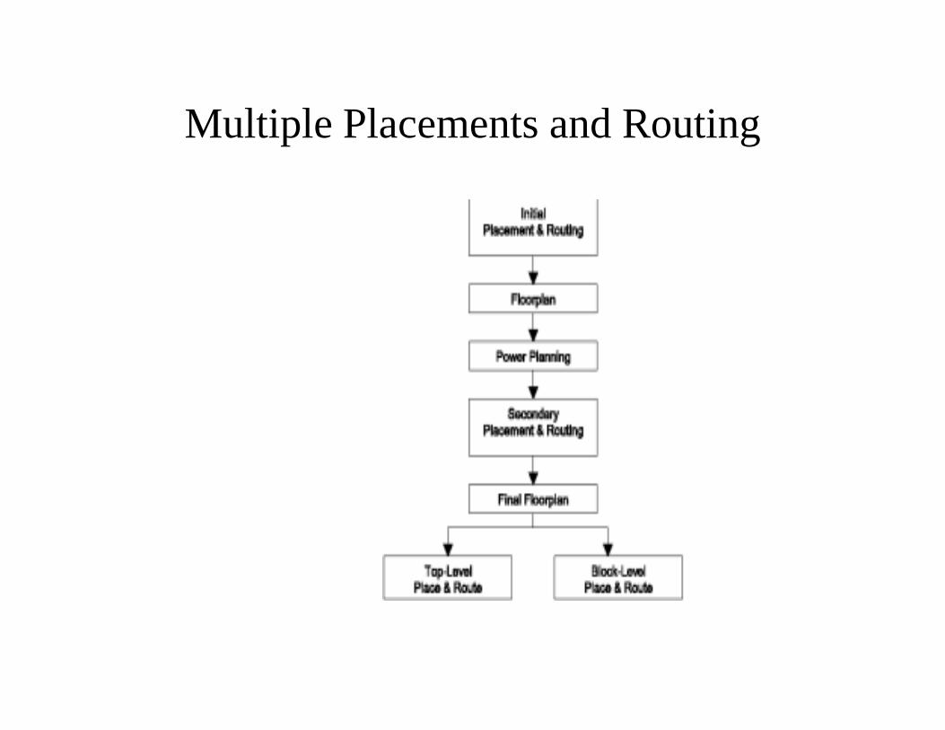
Multiple Placements and Routing
Modern physical design techniques-
• In the age of deep submicron design, where 10+ million gates of logic have to fit on a single device running at 250+ MHz, traditional physical-design techniques are not capable of handling these new challenges. The problems with the traditional physical-design techniques can be summarized as follows :
• Timing closure is either unachievable or takes too long to finish.
• Too many iterations between front end and back end for each design.
• Unroutable designs for the target die size .• As the device geometries shrink to 0.11 micron and beyond,
new tools, techniques, and methodologies are needed to overcome the problems we face with traditional approaches.
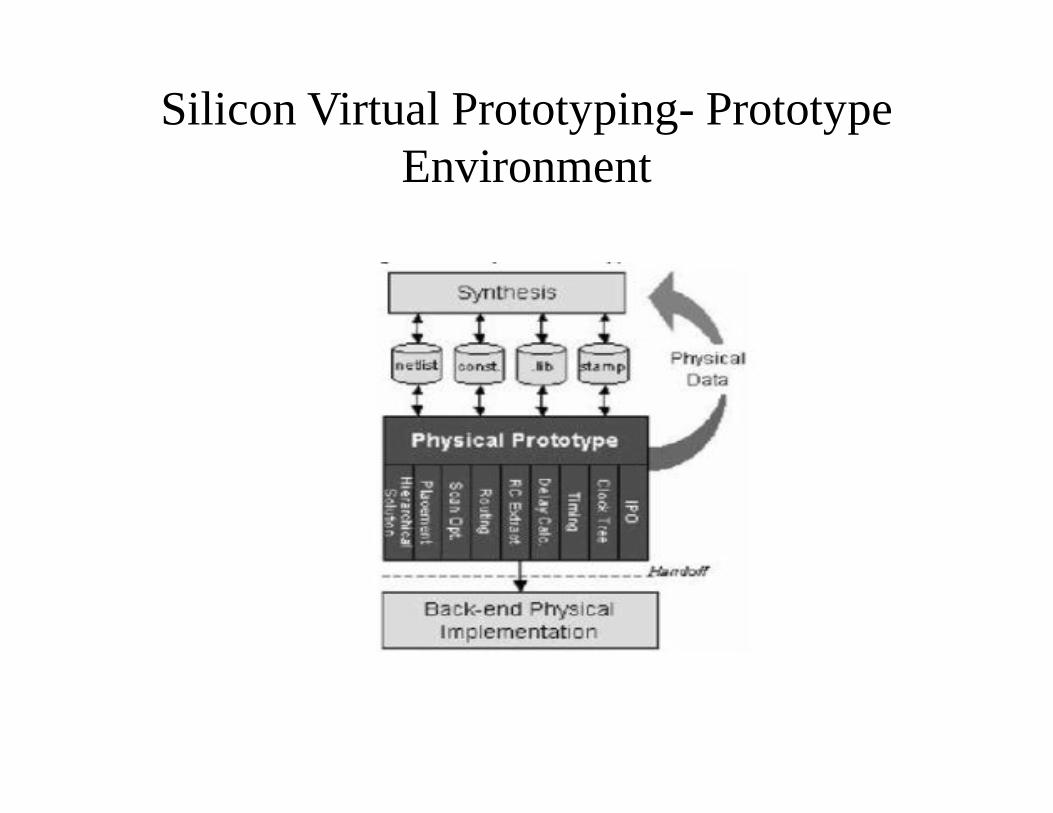
Silicon Virtual Prototyping- Prototype Environment
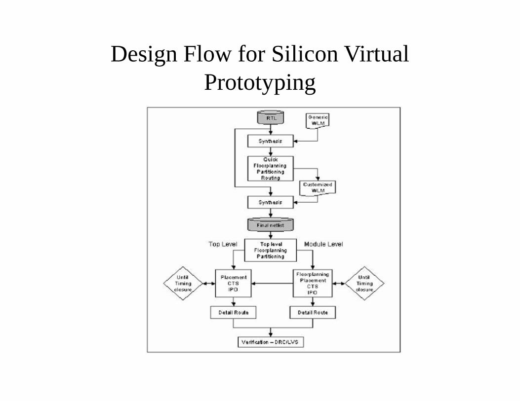
Design Flow for Silicon Virtual Prototyping
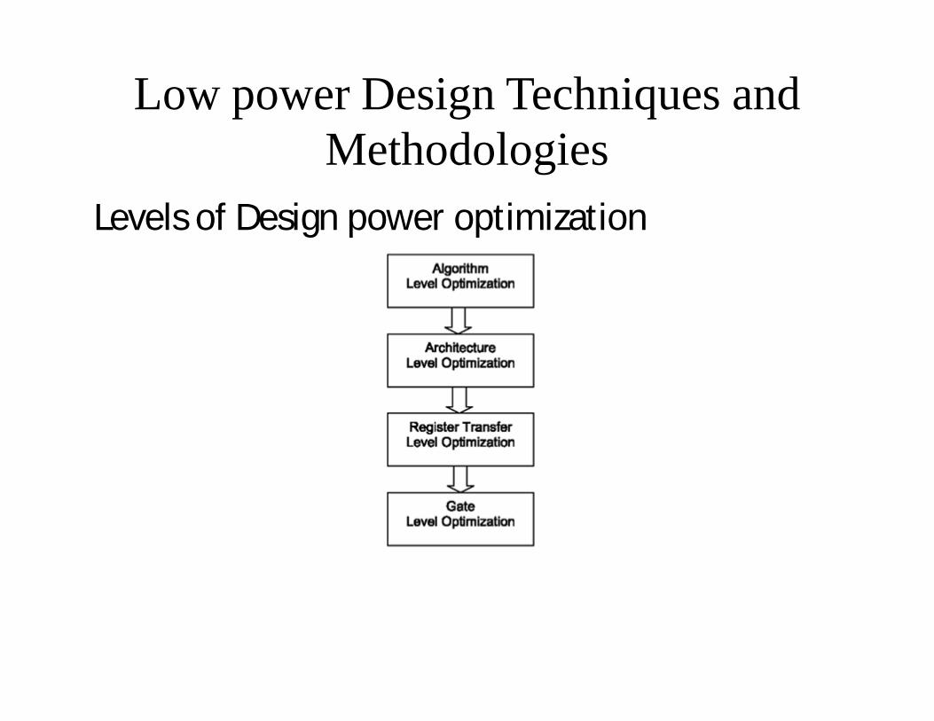
Low power Design Techniques and Methodologies
Levels of Design power optimization
Low power Design Techniques and Methodologies
• Low-power techniques vary depending on the level of the design targeted, ranging from semiconductor technology to the higher levels of abstraction. These abstraction levels are classified as algorithm, architecture, RTL, gate, and transistor levels.
• Higher levels of design abstraction shown in provide larger amounts of power reduction for chip designs. In higher levels of abstraction, such as algorithm level, designers have a greater degree
Low Power Design Techniques
RESEARCH EFFECTS IN LOW POWER DESIGN
Reduce the Active Load:• Minimize the circuits.• Use more efficient Design.• Charge Recycling• More efficient layout
Technology Scaling:• Threshold should scale.• Leakage should be reduced.• Dynamic Voltagescaling.
Low Power Design TechniquesReduce Switching activity:• Conditional Clock.• Conditional Precharge.• Switching-off inactive blocks.• Conditional Execution.
Run it Slower:• Use Parallelism.• Less pipeline stag
LOW-POWER DESIGN TOOLS
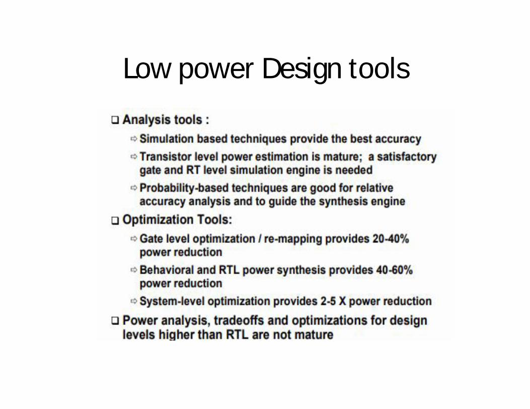
• Numerous EDA tools are available to help IC designers achieve low-power designs. These tools are classified into two main categories:
• Power-analysis and power-estimation tools• Power-optimization tools• Power-estimation tools estimate the power of a specific
design by identifying its high power consuming modules at early stages of the design. These tools give IC designers the ability to make high-level design decisions to reduce power or leave the design untouched based on a set of specific power constraints.
• Power-optimization tools come into play after the decision is made by IC designers to reduce the power.
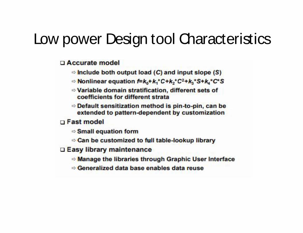
Low power Design tool Characteristics
TIPS AND GUIDELINES FOR LOW-POWER DESIGN
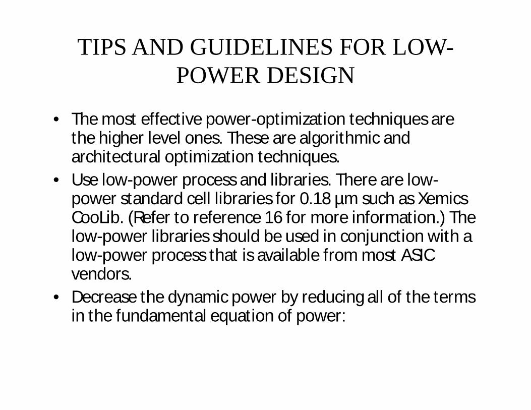
• The most effective power-optimization techniques are the higher level ones. These are algorithmic and architectural optimization techniques.
• Use low-power process and libraries. There are low-power standard cell libraries for 0.18 µm such as XemicsCooLib. (Refer to reference 16 for more information.) The low-power libraries should be used in conjunction with a low-power process that is available from most ASIC vendors.
• Decrease the dynamic power by reducing all of the terms in the fundamental equation of power:
Low power Design tools
Low Power EDA Tools
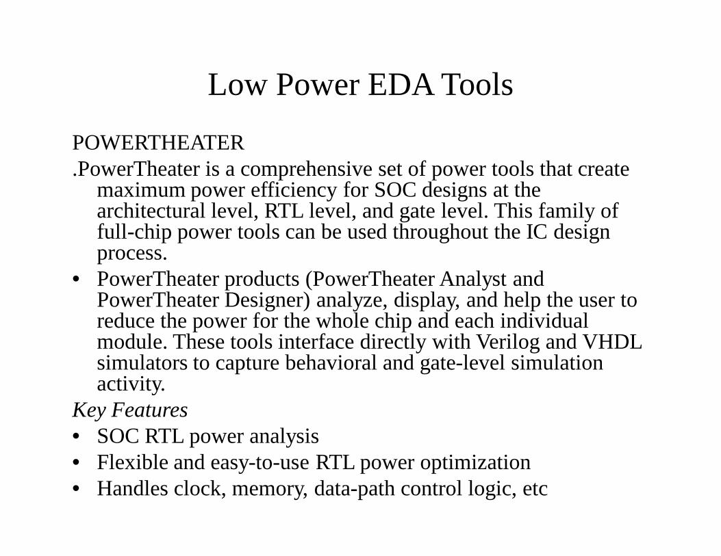
POWERTHEATER.PowerTheater is a comprehensive set of power tools that create
maximum power efficiency for SOC designs at the architectural level, RTL level, and gate level. This family of full-chip power tools can be used throughout the IC design process.
• PowerTheater products (PowerTheater Analyst and PowerTheater Designer) analyze, display, and help the user to reduce the power for the whole chip and each individual module. These tools interface directly with Verilog and VHDL simulators to capture behavioral and gate-level simulation activity.
Key Features• SOC RTL power analysis• Flexible and easy-to-use RTL power optimization• Handles clock, memory, data-path control logic, etc
Low Power EDA ToolsPOWERTHEATER ANALYST• PowerTheater Analyst, built with proven Watt Watcher
technology, represents a superior alternative to tedious and error-prone manual methods, such as spreadsheet analysis, as well as gate- and transistor-level methods which require the design to be synthesized in pieces and then simulated at very detailed levels of abstraction.
Low Power EDA ToolsPOWERTHEATER ANALYST
• Using this capability at both RT and gate level, designers can perform detailed power analysis for the entire chip or any set of sub-blocks, including memory, I/O, logic, and clock trees.
• Peak and time-based power is reported on a user-defined time interval, down to the Verilog or VHDL simulation resolution. PowerTheater Analyst addresses issues such as power bus Sizing, electromigration, and reliability
Low Power EDA ToolsPOWERTHEATER DESIGNER• The Power Theater Designer product uses Watt Watcher's
proven RTL estimation technology to build a detailed, quantitative map of the power in the design.
• Power Theater Designer then invokes a suite of patent-pending agents called Watt Bots that automatically measure the impact of many potential power-saving architectural changes. Each Watt Bot is designed to identify a specific type of power reduction opportunity.
• The suite of Watt Bots covers all major types of circuitry in the design, including control, data path, I/O, memory, and clocks. For each opportunity identified, Power Theater Designer proposes specific RTL design modifications and quantifies the power savings that would result, together with certain potential trade-offs.