Advanced Information Preliminary OV6620/OV6120 · white balance, color matrix, windowing, and more,...
31
OmniVision Technologies, Inc. 930 Thompson Place Sunnyvale, CA 94086 U.S.A. Tel: (408) 733-3030 Fax: (408) 733-3061 e-mail: [email protected] Website: http://www.ovt.com OV6620/OV6120 Advanced Information Preliminary Version 1.4, 13 May 2000 Array Elements (CIF) (QCIF) 356 x 292 (176 x 144) Pixel Size 9.0 x 8.2 μm Image Area 3.1 x 2.5 mm Max Frames/Sec Up to 60 FPS Electronic Exposure Up to 500 : 1 (for selected FPS) Scan Mode progressive Gamma Correction 0.45/.55/1.0 Min. Illumination (3000K) OV6620 - < 3 lux @ f1.2 OV6120 - < 0.5 lux @ f1.2 S/N Ratio (Digital Camera Out) > 48 dB (AGC = Off, Gamma = 1) FPN < 0.03% V P-P Dark Current < 0.2 nA/cm 2 Dynamic Range > 72 dB Power Supply 5VDC, ±5% (Anal.) 5VDC or 3.3VDC (DIO) Power Requirements < 80mW Active < 30μW Standby Package 48 pin LCC OV6620/OV6120 PIN ASSIGNMENTS 6 5 4 3 2 1 48 47 46 45 44 43 ASUB VRCAP2 FREX AGCEN RESET SVDD SGND MULT SIO-0 SIO-1 DEVDD DEGND 7 8 9 10 11 12 13 14 15 16 17 18 AGND AVDD PWDN VRCAP1 VRCAP3 SBB VTO ADVDD ADGND VSYNC/CSYS FODD/CLK HREF/VSFRAM 31 32 33 34 35 36 37 38 39 40 41 42 DGND DOVDD PWDB/PCLK CS0/Y7 CS2/Y6 SHARP/Y5 CS1/Y4 RGB/Y3 G2X/Y2 Y1 CBAR/Y0 BW/CHSYNC 19 20 21 22 23 24 25 26 27 28 29 30 *UV7/B8 *UV6/ABKEN *UV5/MIR *UV4 *UV3 *UV2/QCIF *UV1/CCIR656 *UV0/GAMMA XCLK1 XCLK2 DVDD DGND OV6620/OV6120 * Note: Outputs UV0-UV7 are not available on the OV6120. The inputs associated with these respective pins are still functional. General Description The OV6620 (color) and OV6120 (black and white) CMOS Im- age sensors are single-chip video/imaging camera devices designed to provide a high level of functionality in a single, small-footprint package. Both devices incorporate a 352 x 288 image array capable of operating up to 60 frames per second image capture. Proprietary sensor technology utilizes ad- vanced algorithms to cancel Fixed Pattern Noise (FPN), elim- inate smearing, and drastically reduce blooming. All needed camera functions including exposure control, gamma, gain, white balance, color matrix, windowing, and more, are pro- grammable through an SCCB (Serial Camera Control Bus) in- terface. Both devices can be programmed to provide image output in either 4-, 8- or 16-bit digital formats. Applications include: Video Conferencing, Video Phone, Vid- eo Mail, Still Image, and PC Multimedia. OV6620 SINGLE-CHIP CMOS CIF COLOR DIGITAL CAMERA OV6120 SINGLE-CHIP CMOS CIF B&W DIGITAL CAMERA Features n 101,376 pixels, 1/4” lens, CIF/QCIF format n Progressive scan read out n Data format - YCrCb 4:2:2, GRB 4:2:2, RGB Raw Data n 8/16 bit video data: CCIR601, CCIR656, ZV port n Wide dynamic range, anti-blooming, zero smearing n Electronic exposure / Gain / white balance control n Image enhancement - brightness, contrast, gamma, saturation, sharpness, window, etc. n Internal/external synchronization n Frame exposure/line exposure option n 5-Volt operation, low power dissipation – < 80 mW active power – < 10 μA in power-save mode n Gamma correction (0.45/0.55/1.00) n SCCB programmable (400 kb/s): – color saturation, brightness, contrast, white balance, exposure time, gain
-
Upload
truongtuong -
Category
Documents
-
view
213 -
download
0
Transcript of Advanced Information Preliminary OV6620/OV6120 · white balance, color matrix, windowing, and more,...

OmniVision Technologies, Inc. 930 Thompson Place Sunnyvale, CA 94086 U.S.A.Tel: (408) 733-3030 Fax: (408) 733-3061e-mail: [email protected]: http://www.ovt.com
OV6620/OV6120
Advanced InformationPreliminary
Version 1.4, 13 May 2000
Array Elements (CIF)(QCIF)
356 x 292(176 x 144)
Pixel Size 9.0 x 8.2 µm
Image Area 3.1 x 2.5 mm
Max Frames/Sec Up to 60 FPS
ElectronicExposure
Up to 500 : 1(for selected FPS)
Scan Mode progressive
Gamma Correction 0.45/.55/1.0
Min. Illumination(3000K)
OV6620 - < 3 lux @ f1.2 OV6120 - < 0.5 lux @ f1.2
S/N Ratio(Digital Camera Out)
> 48 dB(AGC = Off, Gamma = 1)
FPN < 0.03% VP-P
Dark Current < 0.2 nA/cm2
Dynamic Range > 72 dB
Power Supply 5VDC, ±5% (Anal.)5VDC or 3.3VDC (DIO)
PowerRequirements
< 80mW Active< 30µW Standby
Package 48 pin LCCOV6620/OV6120 PIN ASSIGNMENTS
6 5 4 3 2 1 48 47 46 45 44 43
AS
UB
VR
CA
P2
FR
EX
AG
CE
NR
ES
ET
SV
DD
SG
ND
MU
LT
SIO
-0S
IO-1
DE
VD
DD
EG
ND
789101112131415161718
AGNDAVDDPWDN
VRCAP1VRCAP3
SBBVTO
ADVDDADGND
VSYNC/CSYS FODD/CLK
HREF/VSFRAM 313233343536373839404142
DGNDDOVDDPWDB/PCLKCS0/Y7CS2/Y6SHARP/Y5CS1/Y4RGB/Y3G2X/Y2Y1CBAR/Y0BW/CHSYNC
19 20 21 22 23 24 25 26 27 28 29 30
*UV
7/B
8*U
V6/
AB
KE
N*U
V5/
MIR
*UV
4*U
V3
*UV
2/Q
CIF
*UV
1/C
CIR
656
*UV
0/G
AM
MA
XC
LK
1X
CL
K2
DV
DD
DG
ND
OV6620/OV6120
* Note: Outputs UV0-UV7 are not available on the OV6120. The inputs associated with these respective pins are still functional.
General DescriptionThe OV6620 (color) and OV6120 (black and white) CMOS Im-age sensors are single-chip video/imaging camera devicesdesigned to provide a high level of functionality in a single,small-footprint package. Both devices incorporate a 352 x 288image array capable of operating up to 60 frames per secondimage capture. Proprietary sensor technology utilizes ad-vanced algorithms to cancel Fixed Pattern Noise (FPN), elim-inate smearing, and drastically reduce blooming. All needed
camera functions including exposure control, gamma, gain,white balance, color matrix, windowing, and more, are pro-grammable through an SCCB (Serial Camera Control Bus) in-terface. Both devices can be programmed to provide imageoutput in either 4-, 8- or 16-bit digital formats.
Applications include: Video Conferencing, Video Phone, Vid-eo Mail, Still Image, and PC Multimedia.
OV6620 SINGLE-CHIP CMOS CIF COLOR DIGITAL CAMERAOV6120 SINGLE-CHIP CMOS CIF B&W DIGITAL CAMERA
Featuresn 101,376 pixels, 1/4” lens, CIF/QCIF formatn Progressive scan read out
n Data format - YCrCb 4:2:2, GRB 4:2:2, RGB Raw Datan 8/16 bit video data: CCIR601, CCIR656, ZV portn Wide dynamic range, anti-blooming, zero smearingn Electronic exposure / Gain / white balance controln Image enhancement - brightness, contrast, gamma,
saturation, sharpness, window, etc.n Internal/external synchronization
n Frame exposure/line exposure optionn 5-Volt operation, low power dissipation
– < 80 mW active power
– < 10 µA in power-save mode
n Gamma correction (0.45/0.55/1.00)n SCCB programmable (400 kb/s):
– color saturation, brightness, contrast, white balance,exposure time, gain

Table 1. Pin Description
Pin No. Name Pin Type Function/Description
01 SVDD Vin Array power (+5VDC)
02 RESET Function(Default = 0)
Chip Reset, active high
03 AGCEN Function(Default = 0)
Automatic Gain Control (AGC) selection“0” - Disable AGC“1” - Enable AGC
NOTE: This function is disabled when OV6620/OV6120 sensor is config-ured in SCCB mode.
04 FREX Function(Default = 0)
Frame Exposure Control“0” - Disable Frame Exposure Control“1” - Enable Frame Exposure Control
05 VRCAP2 Vref (2.5V) Array reference. Connect to ground through 0.1 uF capacitor.
06 ASUB Vin Analog substrate voltage
07 AGND Vin Analog ground
08 AVDD Vin Analog power supply (+5VDC)
09 PWDN Function(Default = 0)
Power down mode selection“0” - normal mode“1” - power down mode
10 VrCAP1 N/C Internal voltage reference. Connect to ground through 0.1 µF capacitor.
11 VrCAP3 Internal voltage reference. Connect to ground through 1 µF capacitor.
12 SBB Function(Default = 0)
SCCB (Serial Camera Control Bus) enable selection“0” - Enable SCCB“1” - Enable autocontrol mode
13 VTO O Luminance Composite Signal Output
14 ADVDD Vin Analog power supply (+5VDC)
15 ADGND Vin Analog signal ground
16 VSYNC/CSYS I/O Vertical sync output. At power up, read as CSYS.
17 FODD/CLK I/O Field ID FODD output or main clock output
18 HREF/VSFRAM I/O HREF output. At power up, read as VSFRAM
19 *UV7/B8 I/O Bit 7 of U video component output. At power up, sampled as B8.* Note: Output UV7 is not available on the OV6120 sensor
20 *UV6/ABKEN I/O Bit 6 of U video component output. At power up, sampled as ABKEN.* Note: Output UV6 is not available on the OV6120 sensor
21 *UV5/MIR I/O Bit 5 of U video component output. At power up, sampled as MIR.* Note: Output UV5 is not available on the OV6120 sensor
22 *UV4 I/O Bit 4of U video component output. * Note: This output (UV4) is not available on the OV6120 sensor
OV6620/OV6120 SINGLE IC CMOS COLOR AND B/W DIGITAL CAMERAS
OMNIVISION TECHNOLOGIES, Inc.

13 May 2000 Version 1.4 3
OV6620/OV6120 SINGLE IC CMOS COLOR AND B/W DIGITAL CAMERAS
OMNIVISION TECHNOLOGIES, Inc.
Advanced InformationPreliminary
23 *UV3 I/O Bit 3 of U video component output.* Note: This output (UV3) is not available on the OV6120 sensor
24 *UV2/QCIF I/O Bit 2 of U video component output. At power up, sampled as QCIF.* Note: Output UV2 is not available on the OV6120 sensor
25 *UV1/CC656 I/O Bit 1 of U video component output. At power up, sampled as CC656.* Note: Output UV1 is not available on the OV6120 sensor
26 *UV0/GAMMA I/O Bit 0 of U video component output. At power up, sampled as GAMMA.* Note: Output UV0 is not available on the OV6120 sensor
27 XCLK1 I Crystal clock input
28 XCLK2 O Crystal clock output
29 DVDD Vin Digital power supply (+5VDC)
30 DGND Vin Digital ground
31 DOGND Vin Digital interface output buffer ground
32 DOVDD Vin Digital interface output buffer power supply (+5VDC)
33 PCLK/PWDB I/O PCLK output. At power up sampled as PWDB.
34 Y7/CS0 I/O Bit 7 of Y video component output. At power up, sampled as CS0.
35 Y6/CS2 I/O Bit 6 of Y video component output. At power up, sampled as CS2.
36 Y5/SHARP I/O Bit 5 of Y video component. At power up, sampled as SHARP.
37 Y4/CS1 I/O Bit 4 of Y video component. At power up, sampled as CS1
38 Y3/RGB I/O Bit 3 of Y video component output. At power up, sampled as RGB.
39 Y2/G2X I/O Bit 2 of Y video component output. At power up, sampled as G2X.
40 Y1 I/O Bit 1 of Y video component output.
41 Y0/CBAR I/O Bit 0 of Y video component output. At power up, sampled as CBAR.
42 CHSYNC/BW I/O CHSYNC output. At power up, sampled as BW.
43 DEGND Vin Decoder ground.
44 DEVDD Vin Decoder power supply (+5VDC)
45 SIO-1 I SCCB serial interface clock input
46 SIO-0 I/O SCCB serial interface data input and output.
47 MULT Function(Default = 0)
SCCB slave selection“0” - Select single slave ID“1” - Enable multiple (8) slaves
48 SGND Vin Array ground
Table 1. Pin Description
Pin No. Name Pin Type Function/Description

OV6620/OV6120
4 Version 1.4 13 May 2000
SINGLE IC CMOS COLOR AND B/W DIGITAL CAMERAS
OMNIVISION TECHNOLOGIES, Inc.
Advanced InformationPreliminary
Figure 1. OV6620/OV6120 CMOS Image Sensor Block Diagram
AWBTH/
VTO
image
row
sel
ect
column sense amp
array
CbCr
Y
GAMMA
whiteexposuredetect
WBcontrol
balancedetect
AWBAGCEN
XVCLK1
(356x292)
1/2
sys-clk
rgb
FODD
VSYNCHREF
PCLK
video timing generator
FZEX
exposure control
FREZ
CHSYNC
mx
ADC
form
atte
r
Y(7:0)
*UV(7:0)
SCCBinterface
SIO-1 SIO-0
registers
vide
o po
rt
ADC
SBB
analog processing
FSIN
MIR
DENB
mx
PROGAWBTM
* Note: Outputs UV(7:0) are notavailable on the OV6120.
1.1 Overview
Referring to Figure 1, OV6620/OV6120 CMOS ImageSensor Block Diagram below, the OV6620 sensor in-cludes a 356 x 292 resolution image array, an analogsignal processor, dual 8-bit Analog-to-Digital convert-ers, analog video multiplexer, digital data formatter andvideo port, SCCB interface and registers, digital controlsincluding timing block, exposure, and black and whitebalance.
The OV6620/OV6120 sensor is a 1/4-inch CMOS imag-ing device. The sensor contains approximately 101,376pixels. Its design is based on a field integration read-outsystem with line-by-line transfer and an electronic shut-ter with a synchronous pixel read out scheme. The colorfilter of the sensor consists of a primary color RG/GB ar-ray arranged in line-alternating fashion.
1. Functional Description(Note: References to color features do not apply to the OV6120 B&W Digital Image Sensor.)
13 May 2000 Version 1.4 5
OV6620/OV6120 SINGLE IC CMOS COLOR AND B/W DIGITAL CAMERAS
OMNIVISION TECHNOLOGIES, Inc.
Advanced InformationPreliminary
1.2 Analog Processor Circuits
1.2.1 Overview
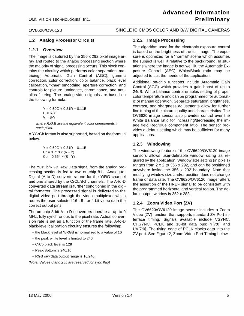
The image is captured by the 356 x 292 pixel image ar-ray and routed to the analog processing section wherethe majority of signal processing occurs. This block con-tains the circuitry which performs color separation, ma-trixing, Automatic Gain Control (AGC), gammacorrection, color correction, color balance, black levelcalibration, “knee” smoothing, aperture correction, andcontrols for picture luminance, chrominance, and anti-alias filtering. The analog video signals are based onthe following formula:
Y = 0.59G + 0.31R + 0.11BU = R-YV = B-Y
where R,G,B are the equivalent color components ineach pixel.
A YCrCb format is also supported, based on the formulabelow:
Y = 0.59G + 0.31R + 0.11BCr = 0.713 x (R - Y)Cb = 0.564 x (B - Y)
The YCrCb/RGB Raw Data signal from the analog pro-cessing section is fed to two on-chip 8-bit Analog-to-Digital (A-to-D) converters: one for the Y/RG channeland one shared by the CrCb/BG channels. The A-to-Dconverted data stream is further conditioned in the digi-tal formatter. The processed signal is delivered to thedigital video port through the video multiplexer whichroutes the user-selected 16-, 8-, or 4-bit video data thecorrect output pins.
The on-chip 8-bit A-to-D converters operate at up to 9MHz, fully synchronous to the pixel rate. Actual conver-sion rate is set as a function of the frame rate. A-to-Dblack-level calibration circuitry ensures the following:
– the black level of Y/RGB is normalized to a value of 16
– the peak white level is limited to 240
– CrCb black level is 128
– Peak/Bottom is 240/16
– RGB raw data output range is 16/240
(Note: Values 0 and 255 are reserved for sync flag)
1.2.2 Image Processing
The algorithm used for the electronic exposure controlis based on the brightness of the full image. The expo-sure is optimized for a “normal” scene which assumesthe subject is well lit relative to the background. In situ-ations where the image is not well lit, the Automatic Ex-posure Control (AEC) White/Black ratio may beadjusted to suit the needs of the application.
Additional on-chip functions include Automatic GainControl (AGC) which provides a gain boost of up to24dB. White balance control enables setting of propercolor temperature and can be programmed for automat-ic or manual operation. Separate saturation, brightness,contrast, and sharpness adjustments allow for furtherfine tuning of the picture quality and characteristics. TheOV6620 image sensor also provides control over theWhite Balance ratio for increasing/decreasing the im-age field Red/Blue component ratio. The sensor pro-vides a default setting which may be sufficient for manyapplications.
1.2.3 Windowing
The windowing feature of the OV6620/OV6120 imagesensors allows user-definable window sizing as re-quired by the application. Window size setting (in pixels)ranges from 2 x 2 to 356 x 292, and can be positionedanywhere inside the 356 x 292 boundary. Note thatmodifying window size and/or position does not changeframe or data rate. The OV6620/OV6120 imager altersthe assertion of the HREF signal to be consistent withthe programmed horizontal and vertical region. The de-fault output window is 352 x 288.
1.2.4 Zoom Video Port (ZV)
The OV6620/OV6120 image sensor includes a ZoomVideo (ZV) function that supports standard ZV Port in-terface timing. Signals available include VSYNC,CHSYNC, PCLK and 16-bit data bus: Y[7:0] andUV[7:0]. The rising edge of PCLK clocks data into theZV port. See Figure 2, Zoom Video Port Timing below.

OV6620/OV6120
6 Version 1.4 13 May 2000
SINGLE IC CMOS COLOR AND B/W DIGITAL CAMERAS
OMNIVISION TECHNOLOGIES, Inc.
Advanced InformationPreliminary
Figure 2. Zoom Video Port TimingNotes:
1. Zoom Video Port format output signal includes:VSYNC: Vertical sync pulse.HREF: Horizontal valid data output window.PCLK: Pixel clock used to clock valid data and CHSYNC into Zoom V Port. Default frequency is 8.86MHz when use 17.73MHz as system clock. Rising edge of PCLK is used to clock the 16 Bit data.Y[7:0]: 8 Bit luminance data bus.UV[7:0]: 8 Bit chrominance data bus.
2. All timing parameters are provided in Table 13. Zoom Video Port AC Parameters
VSYNC
PCLK
Y[7:0]UV[7:0]
/
HREF
351 352
t8 t8
Even Field 1(FODD=0)
Odd Field(FODD=1)
t6t7
t1
t2
t3t4
Horizontal Timing
VSYNC
Y[7:0]/UV[7:0]
Valid Data
1 LineTvs Tve
t5
Tline
1 2
13 May 2000 Version 1.4 7
OV6620/OV6120 SINGLE IC CMOS COLOR AND B/W DIGITAL CAMERAS
OMNIVISION TECHNOLOGIES, Inc.
Advanced InformationPreliminary
1.2.5 QCIF Format
A QCIF mode is available for applications where highresolution image capture is not required. When pro-grammed in this mode, the pixel rate is reduced by one-half. Default resolution is 176 x 144 pixels and can beuser-programmed for other resolutions. Refer to Table7. QCIF Digital Output Format (YUV, beginning of line)and Table 8. QCIF Digital Output Format (RGB Raw Da-ta, Beginning of Line) for further information.
1.2.6 Video Output
The video output port of the OV6620/OV6120 imagesensors provides a number of output format/standardoptions to suit many different application requirements.Table 2. Digital Output Formats, below, indicates theoutput formats available. These formats are user pro-grammable through the SCCB interface (See Section3.1 SCCB Bus Protocol Format).
The OV6620/OV6120 imager supports both CCIR601and CCIR656 output formats in the following configura-tions (See Table 3. 4:2:2 16-bit Format for further de-tails):
– 16-bit, 4:2:2 format
(This mode complies with the 60/50 Hz CCIR601 tim-ing standard. See Table 3. 4:2:2 16-bit Format be-low)
– 8-bit data mode
(In this mode, video information is output in Cb Y CrY order using the Y port only and running at twice thepixel rate during which the UV port is inactive. SeeTable 4. 4:2:2 8-bit Format below)
– 4-bit nibble mode
(In the nibble mode, video output data appears at bitsY4-Y7. The clock rate for the output runs at twice thenormal output speed when in B/W mode, and 4 timesthe normal output speed in when in color mode.)
– 704 x 288 format
(When programmed for this mode, the OV6620/OV6120 pixel clock is doubled and the video outputsequence is Y0Y0Y1Y1 ... and U0U0V0V0 ... SeeFigure 3, Pixel Data Bus (YUV Output), below.)
The OV6620/OV6120 imaging devices provide VSYNC,HREF, PCLK, FODD, CHSYNC as standard output vid-eo timing signals.
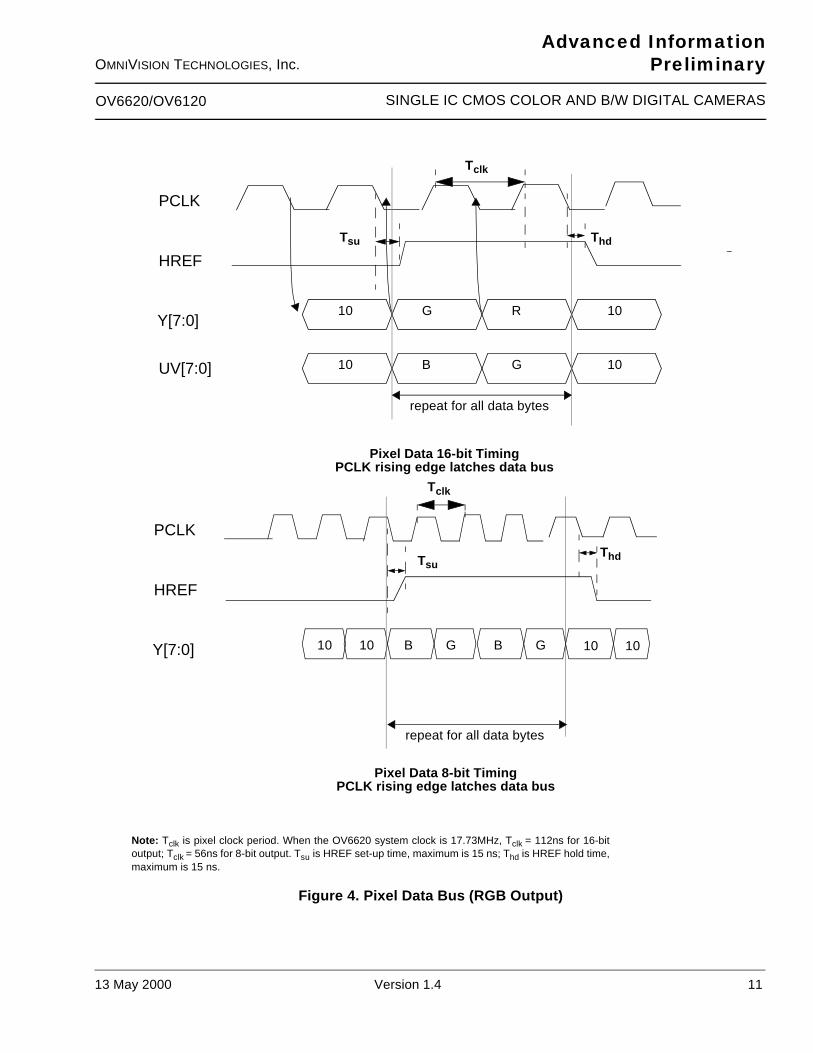
The OV6620/OV6120 image sensor can also be pro-grammed to provide video output in RGB Raw Data 16-bit/8-bit/4-bit format. The output sequence is matched tothe OV6620 Color Filter Pattern (See Section Figure 4.Pixel Data Bus (RGB Output), below):
– Y channel output sequence is G R G R
– UV channel output sequence is B G B G
For 8-bit RGB Raw Data video output appears on the Ychannel (with an output sequence of B G R G) and theUV channel is disabled.
In RGB Raw Data CCIR656 modes, the OV6620/OV6120 imager asserts SAV (Start of Active Video) andEAV (End of Active Video) to indicate the beginning andthe ending of HREF window. As a result, SAV and EAVchange with the active pixel window. The 8-bit RGB rawdata is also accessible without SAV and EAV informa-tion.
The OV6620/OV6120 imagers offer flexibility in YUVoutput format. The devices may be programmed asstandard YUV 4:2:2. These devices may be configuredto “swap” the U V sequence. When swapped, the UVchannel output format for 16-bit configurations be-comes:
– V U V U...etc.
and for 8-bit configurations becomes:
– V Y U Y ...etc.
A third format is available for the 8-bit configurationsand OV6620/OV6120 enables the Y/UV sequenceswap:
– Y U Y V ...etc.
The OV6620 color single-IC camera can be configuredfor use as a black and white imaging device. In thismode, vertical resolution is greater than in color. Videodata output is provided at the Y port (pins 34:41) and theUV port is tri-stated. The data (Y/RGB) output rate isequivalent to operating in 16-bit mode.
The Y/UV or RGB output byte MSB and LSB can be re-verse-ordered on the OV6620/OV6120 device. The Y7- Y0 default sequence sets Y7 as MSB and Y0 as LSB.Programming a reverse order configuration sets Y7 asLSB and Y0 is MSB, with bits Y2-Y6 reversed-orderedappropriately.

OV6620/OV6120
8 Version 1.4 13 May 2000
SINGLE IC CMOS COLOR AND B/W DIGITAL CAMERAS
OMNIVISION TECHNOLOGIES, Inc.
Advanced InformationPreliminary
Notes:
(“Y” indicates mode/combination is supported by OV6620/OV6120.)1. When in RGB CCIR656 format, output is 8 bits. SAV and EAV are inserted at the beginning and ending of
HREF, which synchronize the acquisition of Vsync and Hsync. In this format, an 8-bit data bus configuration(without VSYNC and CHSYNC) may be used.
2. Y/UV swap is valid only in 8-bit mode. Y channel output sequence is Y U Y V...3. In YUV format, U/V swap means UV channel output sequence swap. V U V U... for 16 bit; V Y U Y ... for 8-bit. 4. In RGB format, U/V swap means neighbor row B R output sequence swap. Refer to
RGB raw data output format for further details
Table 2. Digital Output Formats
Resolution Pixel Clock 352 x 288 704 x 288 176 x 144
YUV
4:2:2
16-bit Y Y Y
8-bit Y Y Y
CCIR656 Y Y Y
Nibble Y Y Y
RGB 16-bit Y Y Y
8-bit Y Y Y
CCIR6561 Y Y Y
Nibble Y Y Y
Y/UV
swap2
16-bit
8-bit Y Y Y
U/V
swap
YUV3 Y Y Y
RGB4 Y Y Y
YG 16-bit Y Y Y
8-bit
One
Line
16-bit Y
8-bit
MSB/LSB swap5 Y Y Y

13 May 2000 Version 1.4 9
OV6620/OV6120 SINGLE IC CMOS COLOR AND B/W DIGITAL CAMERAS
OMNIVISION TECHNOLOGIES, Inc.
Advanced InformationPreliminary
Table 3. 4:2:2 16-bit Format
Data Bus Pixel Byte Sequence
Y7 Y7 Y7 Y7 Y7 Y7 Y7
Y6 Y6 Y6 Y6 Y6 Y6 Y6
Y5 Y5 Y5 Y5 Y5 Y5 Y5
Y4 Y4 Y4 Y4 Y4 Y4 Y4
Y3 Y3 Y3 Y3 Y3 Y3 Y3
Y2 Y2 Y2 Y2 Y2 Y2 Y2
Y1 Y1 Y1 Y1 Y1 Y1 Y1
Y0 Y0 Y0 Y0 Y0 Y0 Y0
UV7 U7 V7 U7 V7 U7 V7
UV6 U6 V6 U6 V6 U6 V6
UV5 U5 V5 U5 V5 U5 V5
UV4 U4 V4 U4 V4 U4 V4
UV3 U3 V3 U3 V3 U3 V3
UV2 U2 V2 U2 V2 U2 V2
UV1 U1 V1 U1 V1 U1 V1
UV0 U0 V0 U0 V0 U0 V0
Y FRAME 0 1 2 3 4 5
UV FRAME 0 2 4
Table 4. 4:2:2 8-bit Format
Data Bus Pixel Byte Sequence
Y7 U7 Y7 V7 Y7 U7 Y7 V7 Y7
Y6 U6 Y6 V6 Y6 U6 Y6 V6 Y6
Y5 U5 Y5 V5 Y5 U5 Y5 V5 Y5
Y4 U4 Y4 V4 Y4 U4 Y4 V4 Y4
Y3 U3 Y3 V3 Y3 U3 Y3 V3 Y3
Y2 U2 Y2 V2 Y2 U2 Y2 V2 Y2
Y1 U1 Y1 V1 Y1 U1 Y1 V1 Y1
Y0 U0 Y0 V0 Y0 U0 Y0 V0 Y0
Y FRAME 0 1 2 3
UV FRAME 0 1 2 3

OV6620/OV6120
10 Version 1.4 13 May 2000
SINGLE IC CMOS COLOR AND B/W DIGITAL CAMERAS
OMNIVISION TECHNOLOGIES, Inc.
Advanced InformationPreliminary
Figure 3. Pixel Data Bus (YUV Output)
Y[7:0]
PCLK
HREF
UV[7:0]
10 10Y Y
80 80U V
repeat for all data bytes
Pixel Data 16-bit Timing
Y[7:0]
PCLK
HREF
repeat for all data bytes
Pixel Data 8-bit Timing
U Y V Y 801010 80
(PCLK rising edge latches data bus)
(PCLK rising edge latches data bus)
Tsu
Thd
Thd
Tclk
Tclk
10
Tsu
Note: Tclk is pixel clock period. When the OV6620 system clock is 17.73 MHz, Tclk = 112 ns for 16-bit
output; Tclk = 56 ns for 8-bit output. Tsu is HREF set-up time, maximum is 15 ns; Thd is HREF hold time,
maximum is 15 ns.
13 May 2000 Version 1.4 11
OV6620/OV6120 SINGLE IC CMOS COLOR AND B/W DIGITAL CAMERAS
OMNIVISION TECHNOLOGIES, Inc.
Advanced InformationPreliminary
Figure 4. Pixel Data Bus (RGB Output)
Y[7:0]
PCLK
HREF
UV[7:0]
10 10G R
10 10B G
repeat for all data bytes
Pixel Data 16-bit Timing
Y[7:0]
PCLK
HREF
10 10B B
repeat for all data bytes
Pixel Data 8-bit Timing
10 G G 10
PCLK rising edge latches data bus
PCLK rising edge latches data bus
Tclk
Tclk
Thd
ThdTsu
Tsu
Note: Tclk is pixel clock period. When the OV6620 system clock is 17.73MHz, Tclk = 112ns for 16-bitoutput; Tclk = 56ns for 8-bit output. Tsu is HREF set-up time, maximum is 15 ns; Thd is HREF hold time,maximum is 15 ns.
OV6620/OV6120
12 Version 1.4 13 May 2000
SINGLE IC CMOS COLOR AND B/W DIGITAL CAMERAS
OMNIVISION TECHNOLOGIES, Inc.
Advanced InformationPreliminary
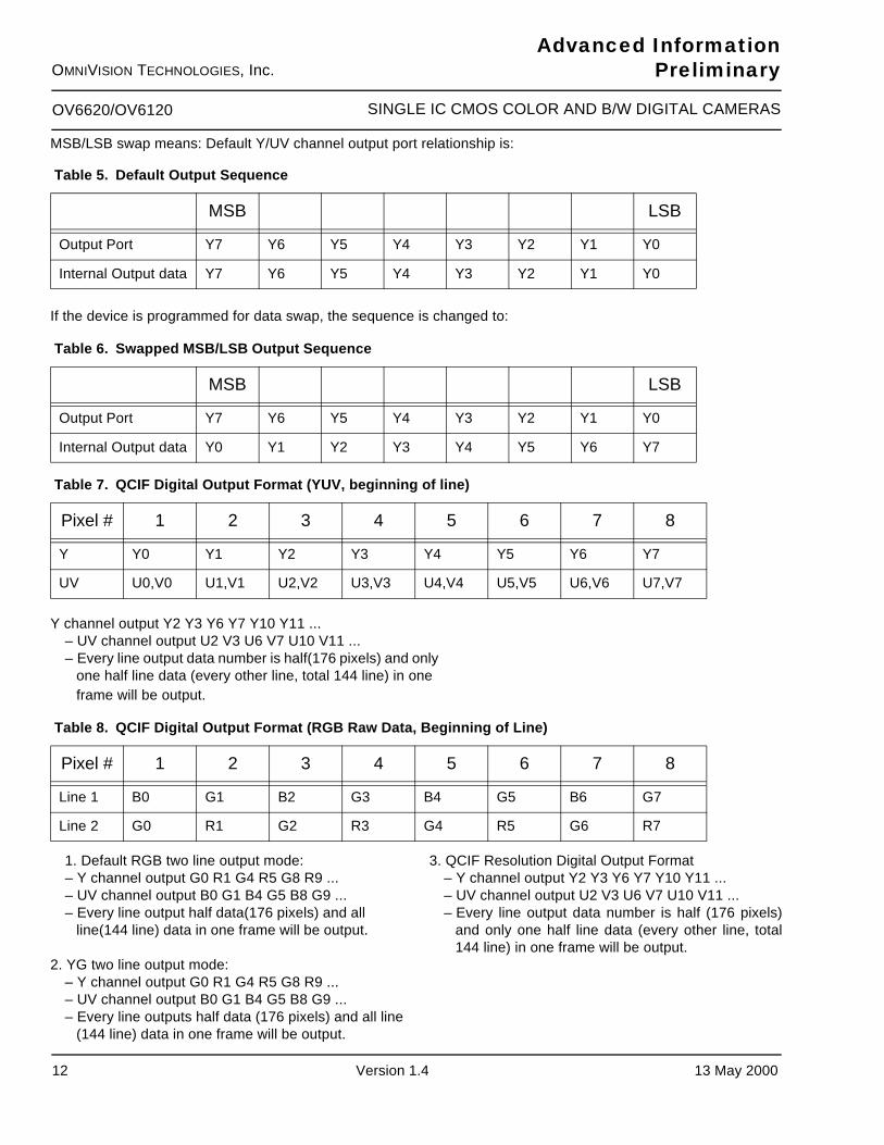
MSB/LSB swap means: Default Y/UV channel output port relationship is:
If the device is programmed for data swap, the sequence is changed to:
Y channel output Y2 Y3 Y6 Y7 Y10 Y11 ... – UV channel output U2 V3 U6 V7 U10 V11 ... – Every line output data number is half(176 pixels) and only
one half line data (every other line, total 144 line) in one frame will be output.
Table 5. Default Output Sequence
MSB LSB
Output Port Y7 Y6 Y5 Y4 Y3 Y2 Y1 Y0
Internal Output data Y7 Y6 Y5 Y4 Y3 Y2 Y1 Y0
Table 6. Swapped MSB/LSB Output Sequence
MSB LSB
Output Port Y7 Y6 Y5 Y4 Y3 Y2 Y1 Y0
Internal Output data Y0 Y1 Y2 Y3 Y4 Y5 Y6 Y7
Table 7. QCIF Digital Output Format (YUV, beginning of line)
Pixel # 1 2 3 4 5 6 7 8
Y Y0 Y1 Y2 Y3 Y4 Y5 Y6 Y7
UV U0,V0 U1,V1 U2,V2 U3,V3 U4,V4 U5,V5 U6,V6 U7,V7
Table 8. QCIF Digital Output Format (RGB Raw Data, Beginning of Line)
Pixel # 1 2 3 4 5 6 7 8
Line 1 B0 G1 B2 G3 B4 G5 B6 G7
Line 2 G0 R1 G2 R3 G4 R5 G6 R7
1. Default RGB two line output mode:– Y channel output G0 R1 G4 R5 G8 R9 ... – UV channel output B0 G1 B4 G5 B8 G9 ...– Every line output half data(176 pixels) and all
line(144 line) data in one frame will be output.
2. YG two line output mode:– Y channel output G0 R1 G4 R5 G8 R9 ... – UV channel output B0 G1 B4 G5 B8 G9 ...– Every line outputs half data (176 pixels) and all line
(144 line) data in one frame will be output.
3. QCIF Resolution Digital Output Format– Y channel output Y2 Y3 Y6 Y7 Y10 Y11 ... – UV channel output U2 V3 U6 V7 U10 V11 ... – Every line output data number is half (176 pixels)
and only one half line data (every other line, total144 line) in one frame will be output.

13 May 2000 Version 1.4 13
OV6620/OV6120 SINGLE IC CMOS COLOR AND B/W DIGITAL CAMERAS
OMNIVISION TECHNOLOGIES, Inc.
Advanced InformationPreliminary
Notes:
A. Y port output data sequence: G R G R G R ... or G G G G ... ; UV port output data sequence: B G B G B G ... or B R B R ... ;Array Color Filter Patter is Bayer-Pattern
B. Output Modes
16-bit Format (HREF total 292)
Default mode:
– 1st HREF Y channel output unstable data, UV output B11 G12 B13 G14 .... – 2nd HREF Y channel output G21 R22 G23 R24 ..., UV output B11 G12 B13 G14 ... – 3rd HREF Y channel output G21 R22 G23 R24 ..., UV output B31 G23 B33 G34 .... – Every line of data is output twice.
YG mode:
– 1st HREF Y and UV output unstable data. – 2nd HREF Y channel output G21 G12 G23 G14 ..., UV output B11 R22 B13 R24 ... – 3rd HREF Y is G21 G32 G23 G34 ..., UV channel is B31 R22 B33 R24 ... – Every line data output twice.
One line mode:
– 1st HREF Y channel output B11 G12 B13 G14 ..., – 2nd HREF Y channel output G21 R22 G23 R24 ..., – UV channel tri-state.
8-bit Format (HREF total 292)
– 1st HREF Y channel output unstable data. – 2nd HREF Y channel output B11 G21 R22 G12 ... – 3rd HREF Y channel output B31 G21 R22 G32 ..., etc.– PCLK timing is double and PCLK rising edge latch data bus. UV channel tri-state. Every line data output twice.
4-bit Nibble Mode Output Format
– Uses higher 4 bits of Y port (Y[7:4]) as output port. – Supports YCrCb/RGB data, CCIR601/CCIR656 timing, Color/B&W. – Output sequence: High order 4 bits followed by lower order 4 bits
Y0h Y0l Y1h Y1l ...U0h U0l V0h V0l ...
For B/W or one-line RGB raw data, the output data clock speed is doubled. For color YUV, output clock is four times that of the 16-bit outputdata. In color mode, sensor must be set to 8-bit mode, and the nibble timing, clock divided by 2.
– Output sequence: U0h U0l Y0h Y0l V0h V0l Y1h Y1l ...
Table 9. RGB Raw Data Format
R\C 1 2 3 4 . 353 354 355 356
1 B11 G12 B13 G14 B G B G
2 G21 R22 G23 R24 G R G R
3 B31 G32 B33 G34 B G B G
4 G41 R42 G43 R44 G R G R
5 B51 G52 B53 G54 B G B G
.
289 B G B G B G B G
290 G R G R G R G R
291 B G B G B G B G
292 G R G R G R G R
OV6620/OV6120
14 Version 1.4 13 May 2000
SINGLE IC CMOS COLOR AND B/W DIGITAL CAMERAS
OMNIVISION TECHNOLOGIES, Inc.
Advanced InformationPreliminary
1.2.7 Slave Mode Operation
The OV6620/OV6120 sensors can be programmable tooperate in slave mode configuration (COMI[6] = 1, de-fault is master mode). HSYNC and VSYNC output sig-nals are provided.
When used as a slave device, the external master mustprovide the OV6620/OV6120 imager with the following:
1. System clock CLK to XCLK1 pin;2. Horizontal sync, Hsync, to CHSYNC pin, positive
assertion;3. Vertical frame sync, Vsync, to VSYNC pin,
positive assertion
When in slave mode, the OV6620/OV6120 tri-statesCHSYNC (pin 42) and VSYNC (pin 16) output pins,which may then be used as input pins. To synchronizemultiple devices, the OV6620/OV6120 image sensorsuse external system clock, CLK, to synchronize externalhorizontal sync, HSYNC, which is then used to synchro-nize external vertical frame sync, Vsync. See Figure 5,Slave Mode External Sync Timing for timing consider-ations.
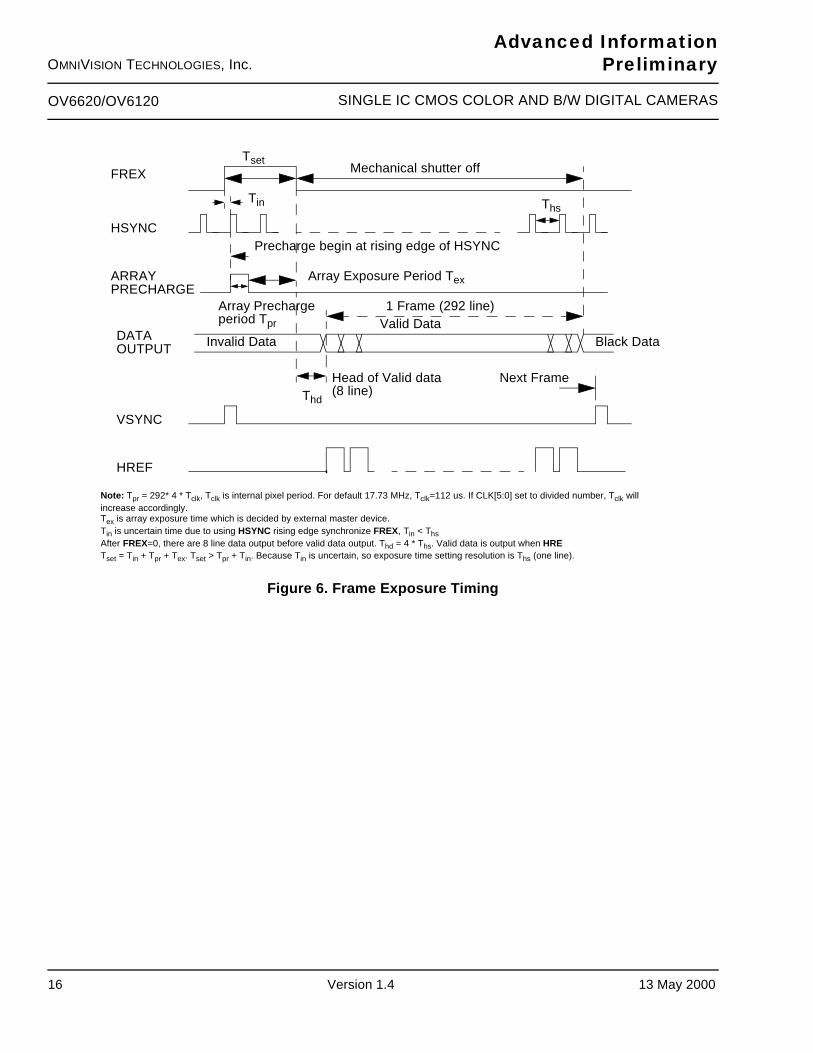
1.2.8 Frame Exposure Mode
The OV6620/OV6120 sensors support frame exposuremode when programmed for Progressive Scan. FREX(pin 4) is asserted by an external master device to setexposure time. When FREX = 1, the OV6620/OV6120pixel array will be quickly precharged. Based on the ex-ternal master’s assertion of FREX, the OV6620/OV6120devices capture the image. When the master de-assertsFREX (FREX = 0), the video output data stream is deliv-ered to the OV6620/OV6120 output port in a line-by-linemanner.
It should be noted that FREX must remain active longenough to ensure the complete image array has beenprecharged.
When data is being output from the OV6620/OV6120image sensor, care must be taken so as not to exposethe image array to light. This may affect the integrity ofthe image data captured. A mechanical shutter synchro-nized with the frame exposure rate can be used to min-imize this situation. Frame exposure mode timing isshown in Section Figure 6. Frame Exposure Timing be-low.
1.2.9 Reset
The OV6620/OV6120 image sensors include a RESETpin (pin 2) which forces a complete hardware reset when
pulled high (Vcc). When a hardware reset occurs, theOV6620/OV6120 sensor clears all registers or setsthem to their default values. Reset may also be initiatedthrough the SCCB interface.
1.2.10 Power Down Mode
Two methods are available for placing the OV6620/OV6120 devices into power-down mode: hardware pow-er down and SCCB/software power down.
To initiate hardware power down the PWDN pin (pin 9)must be tied to high (+5VDC). When this occurs, theOV6620/OV6120 internal device clock is halted and allinternal registers (except SCCB registers) are reset. Inthis mode, current draw is less than 10uA.
Executing a software power down through the SCCB in-terface suspends internal circuit activity, but does haltthe device clock. In this mode, current requirementsdrop to less than 1mA.
1.2.11 Configuring the OV6620/OV6120 Image Sensors
Two methods are provided for configuring the OV6620/OV6120 ICs for specific application requirements.
At power up, the OV6620/OV6120 sensors read the sta-tus of certain pins to determine what, if any, power updefault settings are requested. Once the reading of theexternal pins is completed, the device configures its in-ternal registers according to the specified pins. Not alldevice functions are available for configuration throughexternal pin.
A more flexible and comprehensive method for configur-ing the OV6620/OV6120 ICs is to use its on-chip SCCBregister programming capability. The SCCB interfaceprovides access to all of the device’s programmable in-ternal registers. See Section 3.1 SCCB Bus for furtherdetails about using the SCCB interface on the OV6620/OV6120 camera device.

13 May 2000 Version 1.4 15
OV6620/OV6120 SINGLE IC CMOS COLOR AND B/W DIGITAL CAMERAS
OMNIVISION TECHNOLOGIES, Inc.
Advanced InformationPreliminary
Figure 5. Slave Mode External Sync Timing
CLK
Hsync
Vsync
1 frame = 625 * 472 * Tclk
1 line=472 * Tclk
Tclk
Tvs
Ths
Notes: 1. Ths > 6 * Tclk (2) Ths < Tvs < 472 * Tclk2. Hsync period is 472 * CLK3. Vsync period is 625 * 472 * CLK4. OV6620 will be stable after 1 frame. (2nd Vsync).
OV6620/OV6120
16 Version 1.4 13 May 2000
SINGLE IC CMOS COLOR AND B/W DIGITAL CAMERAS
OMNIVISION TECHNOLOGIES, Inc.
Advanced InformationPreliminary
Figure 6. Frame Exposure Timing
FREX
DATA
HSYNC
OUTPUT
VSYNC
ARRAYPRECHARGE
Black DataInvalid DataValid Data1 Frame (292 line)
Precharge begin at rising edge of HSYNC
Array Exposure Period Tex
Array Prechargeperiod Tpr
Tset
Next Frame
Mechanical shutter off
Head of Valid data
Tin Ths
Thd
HREF
(8 line)
Note: Tpr = 292* 4 * Tclk, Tclk is internal pixel period. For default 17.73 MHz, Tclk=112 us. If CLK[5:0] set to divided number, Tclk will increase accordingly.Tex is array exposure time which is decided by external master device.Tin is uncertain time due to using HSYNC rising edge synchronize FREX, Tin < ThsAfter FREX=0, there are 8 line data output before valid data output. Thd = 4 * Ths. Valid data is output when HRETset = Tin + Tpr + Tex. Tset > Tpr + Tin. Because Tin is uncertain, so exposure time setting resolution is Ths (one line).
13 May 2000 Version 1.4 17
OV6620/OV6120 SINGLE IC CMOS COLOR AND B/W DIGITAL CAMERAS
OMNIVISION TECHNOLOGIES, Inc.
Advanced InformationPreliminary

OV6620/OV6120
18 Version 1.4 13 May 2000
SINGLE IC CMOS COLOR AND B/W DIGITAL CAMERAS
OMNIVISION TECHNOLOGIES, Inc.
Advanced InformationPreliminary
2. Electrical Characteristics
Table 10. DC Characteristics (0oC < TA < 85oC, Voltages referenced to GND)
Symbol Descriptions Max Typ Min Units
Supply
VDD1 Supply voltage- internal analog(DEVDD,ADVDD,AVDD,SVDD,AOVDD,DVDD)
5.25 5.0 4.75 V
VDD2 Supply voltage - internal digital &output digital(DOVDD)
5.53.6
5.03.3
4.53.0
VV
IDD1 Supply Current (@ 50Hz frame rate & 5 volt digi-tal I/O,25pf + 1TTL load on 16 bit data bus)
40 - - mA
IDD2 Standby supply current 10 5 - uA
Digital Inputs
VIL input voltage LOW 0.8 - - V
VIH input voltage HIGH - - 2.0 V
Cin input capacitor 10 - - pF
Digital Outputs - standard load 25pf, 1.2kΩ to 3.0volts
VOH output voltage HIGH - - 2.4 V
VOL output voltage LOW 0.6 - - V
SCCB Inputs -
VIL SIO-0 and SIO-1 (VDD2=5V) 1.5 0 -0.5 V
VIH SIO-0 and SIO-1 (VDD2=5V) Vdd + .5 5 3.0 V
VIL SIO-0 and SIO-1 (VDD2=3V) 1 0 -0.5 V
VIH SIO-0 and SIO-1 (VDD2=3V) 3.5 3 2.5 V
13 May 2000 Version 1.4 19
OV6620/OV6120 SINGLE IC CMOS COLOR AND B/W DIGITAL CAMERAS
OMNIVISION TECHNOLOGIES, Inc.
Advanced InformationPreliminary
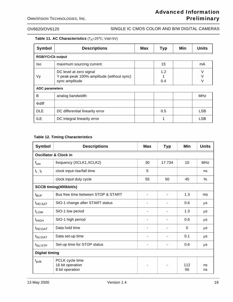
Table 11. AC Characteristics (TA=25oC; Vdd=5V)
Symbol Descriptions Max Typ Min Units
RGB/YCrCb output
Iso maximum sourcing current 15 mA
Vy DC level at zero signalY peak-peak 100% amplitude (without sync)sync amplitude
1.21
0.4
VVV
ADC parameters
B analog bandwidth MHz
Φdiff
DLE DC differential linearity error 0.5 LSB
ILE DC integral linearity error 1 LSB
Table 12. Timing Characteristics
Symbol Descriptions Max Typ Min Units
Oscillator & Clock in
fosc frequency (XCLK1,XCLK2) 30 17.734 10 MHz
tr , tf clock input rise/fall time 5 ns
clock input duty cycle 55 50 45 %
SCCB timing(400kbit/s)
tBUF Bus free time between STOP & START - - 1.3 ms
tHD:SAT SIO-1 change after START status - - 0.6 µs
tLOW SIO-1 low period - - 1.3 µs
tHIGH SIO-1 high period - - 0.6 µs
tHD:DAT Data hold time - - 0 µs
tSU:DAT Data set-up time - - 0.1 µs
tSU:STP Set-up time for STOP status - - 0.6 µs
Digital timing
tpclk PCLK cycle time 16 bit operation8 bit operation
- - 11256
nsns

OV6620/OV6120
20 Version 1.4 13 May 2000
SINGLE IC CMOS COLOR AND B/W DIGITAL CAMERAS
OMNIVISION TECHNOLOGIES, Inc.
Advanced InformationPreliminary
Notes:
1. In Interlaced Mode, there are Even/Odd field different (t8). When In Progressive Scan Mode, only frame timing same asEven field(t8).
2. After VSYNC falling edge, OV6620 will output black reference level, the line number is Tvs, which is the line number be-tween the 1st HREF rising edge after VSYNC falling edge and 1st valid data CHSYNC rising edge. Then valid data, thenblack reference, line number is Tve, which is the line number between last valid data CHSYNC rising edge and 1stCHSYNC rising edge after VSYNC rising edge. The black reference output line number is dependent on vertical windowsetting.
3. When in default setting, Tvs = 14 * Tline, which is changed with register VS[7:0]. VS[7:0] step equal to 1 line.
4. When in default setting, Tve = 4 * Tline for Odd Field, Tve = 3 * Tline for Even Field, which is changed with register VE[7:0].VE[7:0] step equal to 1 line.
tr,tf PCLK rise/fall time 15 - - ns
tpdd PCLK to data valid 15 - - ns
tphd PCLK to HREF delay 20 10 5 ns
Table 13. Zoom Video Port AC Parameters
Symbol Parameter Min. Max.
t1 PCLK fall timing 4 ns 8 ns
t2 PCLK low time 50 ns
t3 PCLK rise time 4 ns 8 ns
t4 PCLK high time 50 ns
t5 PCLK period 106 ns
t6 Y/UV/HREF setup time 10 ns
t7 Y/UV/HREF hold time 20 ns
t8 VSYNC setup/hold time to HREF 1 us
Table 12. Timing Characteristics
Symbol Descriptions Max Typ Min Units
13 May 2000 Version 1.4 21
OV6620/OV6120 SINGLE IC CMOS COLOR AND B/W DIGITAL CAMERAS
OMNIVISION TECHNOLOGIES, Inc.
Advanced InformationPreliminary
31
30
19
18 7
6
43
42
48
+0.0100.060 -0.005
TYP.0.040 ±0.007
TYP.
0.440 ±0.005
0.040 ±0.003
0.085 ±0.010
0.020 ±0.003TYP.
R 0.007548 PLCS
R 0.00754 CORNERS
0.003
0.002
0.020 ±0.002
0.015 ±0.0020.030
0.0030.065 ±0.007
±0.003
Bottom View
Top View
Side View
42
43
6 19
30
31
48
18
1
7
42
43
3130
1918
67
0.006 MAX.0.002 TYP.
0.350 SQ. ±0.0050.430 SQ. ±0.005
0.560 SQ. -0.005+0.012
0.03
6 M
IN.
OV6620/OV6120
22 Version 1.4 13 May 2000
SINGLE IC CMOS COLOR AND B/W DIGITAL CAMERAS
OMNIVISION TECHNOLOGIES, Inc.
Advanced InformationPreliminary
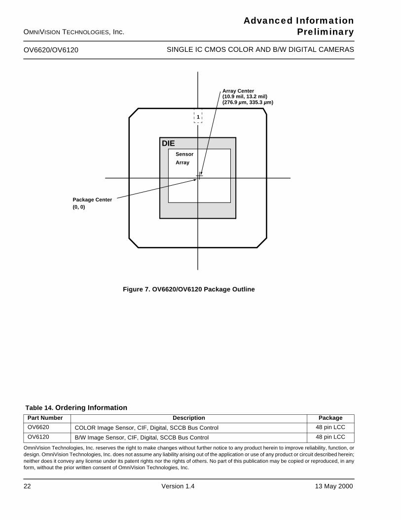
Figure 7. OV6620/OV6120 Package Outline
Table 14. Ordering Information
OmniVision Technologies, Inc. reserves the right to make changes without further notice to any product herein to improve reliability, function, ordesign. OmniVision Technologies, Inc. does not assume any liability arising out of the application or use of any product or circuit described herein;neither does it convey any license under its patent rights nor the rights of others. No part of this publication may be copied or reproduced, in anyform, without the prior written consent of OmniVision Technologies, Inc.
Part Number Description Package
OV6620 COLOR Image Sensor, CIF, Digital, SCCB Bus Control 48 pin LCC
OV6120 B/W Image Sensor, CIF, Digital, SCCB Bus Control 48 pin LCC
1
Sensor
Array
DIE
Package Center(0, 0)
Array Center(10.9 mil, 13.2 mil)(276.9 µm, 335.3 µm)
13 May 2000 Version 1.4 23
OV6620/OV6120 SINGLE IC CMOS COLOR AND B/W DIGITAL CAMERAS
OMNIVISION TECHNOLOGIES, Inc.
Advanced InformationPreliminary
3. SCCB Bus
Many of the functions and configuration registers in theOV6620/OV6120 image sensors are available throughthe SCCB interface. The SCCB port is enabled byasserting the SBB line (pin 12) through a 10K ohm
resistor to VDD. When the SCCB capability is enabled(SBB = 1), the OV6620/OV6120 imager operates as aslave device that supports up to 400 kbps serial trans-fer rate using a 7-bit address/data transfer protocolTherefore, the OV6620/OV6120 sensor takes the read
subaddress from the previous write cycle. In multi-byte write or multi-byte read cycles, the subaddress is automati-cally increment after the first data byte so that continuous locations can be accessed in one bus cycle. A multi-bytecycle overwrites its original subaddress; therefore, if a read cycle immediately follows a multi-byte cycle, you mustinsert a single byte write cycle that provides a new subaddress..
3.1 SCCB Bus Protocol Format
Within each byte, MSB is always transferred first. Read/write control bit is the LSB of the first byte.
The protocol that SIO-0 remain stable during the HIGH period of the SIO-1. Each bit is allowed to change state only
when SIO-1 is LOW. The OV6620/OV6120 SCCB supports multi-byte write and multi-byte read. The master mustsupply the subaddress. in the write cycle, but not in the read cycle.
Therefore, the OV6620/OV6120 sensor takes the read subaddress from the previous write cycle. In multi-byte writeor multi-byte read cycles, the subaddress is automatically increment after the first data byte so that continuouslocations can be accessed in one bus cycle. A multi-byte cycle overwrites its original subaddress; therefore, if aread cycle immediately follows a multi-byte cycle, you must insert a single byte write cycle that provides a new sub-address.
The OV6620/OV6120 imager can be programmed to one-of-eight slave ID addresses. Function pins CS[2:0] pins35, 37, 34, respectively).
The OV6620/OV6120 sensors support both single chip and multiple chip configurations. By asserting MULT (pin 47)high, the sensor can be programmed for up to 8 slave ID addresses. Asserting MULT low configures the OV6620/OV6120 imagers for single ID slave address with address C0 for writes and address C1 for reads. MULT is internallydefaulted to a low condition.
In the write cycle, the second byte in SCCB bus is the subaddress for selecting the individual on-chip registers, andthe third byte is the data associated with this register. Writing to unimplemented subaddress is ignored. In the readcycle, the second byte is the data associated with the previous stored subaddress. Reading of unimplemented sub-address returns unknown.
Table 15. Slave ID Addresses
CS[2:0] 000 001 010 011 100 101 110 111
WRITE ID (hex) C0 C4 C8 CC D0 D4 D8 DC
READ ID (hex) C1 C5 C9 CD D1 D5 D9 DD

OV6620/OV6120
24 Version 1.4 13 May 2000
SINGLE IC CMOS COLOR AND B/W DIGITAL CAMERAS
OMNIVISION TECHNOLOGIES, Inc.
Advanced InformationPreliminary
3.2 Register Set
The table below provides a list and description of avail-able SCCB registers contained in the OV6620/OV6120image sensor.
Table 16. SCCB Registers
Subad-dress(hex)
RegisterDefault (hex)
Read/Write
Descriptions
00 Gain[6:0] 00 RW
AGC Gain ControlGC[7:6] - unimplemented bit, returns ‘X’ when read.GC[5:0] – Storage for the current AGC Gain setting.
This register is updated automatically. If AGC is enabled, the internal control stores the optimal gain value in this register. IF AGC is not enabled, a “00” is stored in this register.
01 Blue[7:0] 80 RW
Blue Gain ControlBLU[7] – “0” decrease gain, “1” increase gain.BLU[6:0] – blue channel gain balance value.
Note: This function is not available on the OV6120 Image Sensor.
02 Red[7:0] 80 RW
Red Gain ControlRED[7] – “0” decrease gain, “1” increase gain.RED[6:0] – red channel balance value.
Note: This function is not available on the OV6120 Image Sensor.
03 Sat 80 RW
Saturation ControlSAT[7:0] – saturation adjustment. “FFh”- highest, “00h”-lowest
Note: This function is not available on the OV6120 Image Sensor.
04 Rsvd04 XX - reserved
05 Cnt 48 RW Contrast ControlCTR[7:0] – contrast adjustment. “FFh”-highest, “00h”-lowest
06 Brt 80 RW Brightness ControlBRT[7:0] – brightness adjustment. “FFh”-highest,“00h”-lowest
07 Sharpness C6 RWSharpness Control
SHP[7:4] – Threshold of sharpness. Range: 0~80mV, Step: 5 mVSHP[3:0] – Sharpness control. Range: 0 ~ 8x, Step: 0.5x
08 Rsvd08 XX - reserved
09 Rsvd09 XX - reserved
0A Rsvd0A XX - reserved
0B Rsvd0B XX - reserved
0C AWB - Blue 20 R/W
White Balance Background: Blue ChannelABLU[7:6] - rsvdABLU[5] - Sign bit.
“0” - decrease background blue component“1” - increase background blue component
ABLU[4:0] - White balance blue ratio adjustment
Note: This function is not available on the OV6120 Image Sensor.
Subad-dress(hex)
RegisterDefault (hex)
Read/Write
Descriptions
13 May 2000 Version 1.4 25
OV6620/OV6120 SINGLE IC CMOS COLOR AND B/W DIGITAL CAMERAS
OMNIVISION TECHNOLOGIES, Inc.
Advanced InformationPreliminary
0E COMR 0D RWCommon Control R
COMR[7] - Analog signal 2x gain control bit. “1” - Additional 2x gain, “0” - normalCOMR[6:0] - Reserved
Subad-dress(hex)
RegisterDefault (hex)
Read/Write
Descriptions
0D AWB - Red 20 R/W
White Balance Background: Red ChannelARED[7:6] - rsvdARED[5] - Sign bit.
“0” - decrease background red component“1” - increase background red component
ABLU[4:0] - White balance red ratio adjustment
Note: This function is not available on the OV6120 Image Sensor.
Subad-dress(hex)
RegisterDefault (hex)
Read/Write
Descriptions
0F COMS 05 RW
Common Control SCOMS[7:6] - ReservedCOMS[5:4] - Black expanding level
“00” - 1.2V, “01” - 1.26V, “10” - 1.3V, “11” - 1.4VCOMS[3:2] - Set high threshold level
“00” - 1.9V, “01” - 2.0V, “10” - 2.1V, “11” - 2.2VCOMS[1:0] - Set low threshold level
“00” - 1.3V, “01” - 1.45V, “10” - 1.5V, “11” - 1.6V
Subad-dress(hex)
RegisterDefault (hex)
Read/Write
Descriptions
10 AEC 9A R
Automatic Exposure ControlAEC[7:0] - Set exposure time
Interlaced: Tex = Tline x AEC[7:0]Progressive: Tex = Tline x AEC[7:0] x 2
11 CLKRC 00 R
Clock Rate ControlCLKRC[7:5] – Sync output polarity selection
“00” - HSYNC=Neg, CHSYNC=Neg, VSYNC=Pos“01” - HSYNC=Neg, CHSYNC=Neg, VSYNC=Neg“10” - HSYNC=Pos, CHSYNC=Neg, VSYNC=Pos“11” - HSYNC=Pos, CHSYNC=Pos, VSYNC=Pos
CLKRC[5:0] – Clock prescalerCLK = (CLK_main / ((CLKRC[5:0] + 1) x 2)) / 2
12 COMA 24 RW
Common Control ACOMA[7] - SRST, “1” initiates soft reset. Initiate soft reset. All registers are set to default val-
ues and chip is reset to known state and resumes normal operation. This bit is automatically cleared after reset.
COMA[6] - MIRR, “1” selects mirror imageCOMA[5] - VSFR, “1” enables AGC,COMA[4] - Digital output format, “1” selects 8-bit: Y U Y V Y U Y VCOMA[3] - Select video data output: “1” - select RGB, “0” - select YCrCbCOMA[2] - Auto White Balance “1” - Enable AWB, “0” - Disable AWBCOMA[1] - Color Bar Test Pattern: “1” - Enable color bar test patternCOMA[0] - reserved
Note: COMA[3] is not programmable on the OV6120 Image Sensor.
Subad-dress(hex)
RegisterDefault (hex)
Read/Write
Descriptions

OV6620/OV6120
26 Version 1.4 13 May 2000
SINGLE IC CMOS COLOR AND B/W DIGITAL CAMERAS
OMNIVISION TECHNOLOGIES, Inc.
Advanced InformationPreliminary
13 COMB 01 RW
Common Control BCOMB[7] - reservedCOMB[6] - reservedCOMB[5] - Select data format. “1” - Select 8-bit format, Y/CrCb and RGB is multiplexed to 8-bit
Y bus, UV bus is tri-stated, “0” - Select 16-bit formatCOMB[4] - “1” - enable digital output in CCIR656 formatCOMB[3] - CHSYNC output: “1” - Horizontal sync, “0” - composite syncCOMB[2] - “1” - Tristate Y and UV busses. “0” - enable both bussesCOMB[1] - “1” - Initiate single frame transferCOMB[0] - “1” - Enable auto adjust mode
Note: COMB[5] is not programmable on the OV6120 Image Sensor.
14 COMC 00 RW
Common Control CCOMC[7] - reservedCOMC[6] - reservedCOMC[5] - QCIF digital output format selection. 1 - 176x144; 0 - 352x288.COMC[4] - Field/Frame vertical sync output in VSYNC port selection: 1 - frame sync, only ODD field vertical sync; 0 - field vertical sync, effect in Interlaced modeCOMC[3] - HREF polarity selection: 0 - HREF positive effective, 1 - HREF negative.COMC[2] - gamma selection: 1 - RGB Gamma on ; 0 - gamma is 1.COMC[1] - reservedCOMC[0] - reserved
15 COMD 01 RW
Common Control DCOMD[7] - reserved bit.COMD[6] - PCLK polarity selection. “0” OV6620 output data at PCLK falling edge and data bus
will be stable at PCLK rising edge; “1” rising edge output data and stable at PCLK fallingedge. When OV6620 work as CCIR656 format, COMB4=1, this bit is disable and shoulduse PCLK rising edge latch data bus.
COMD[5:1] - reserved bit.COMD[0] - U V digital output sequence exchange control. 1 - UV UV ... for 16-bit, U Y V Y ...
for 8-bit; 0 - V U V U ... for 16Bit and V Y U Y ... for 8 Bit.
Note: COMD[0] is not programmable on the OV6120 Image Sensor.
16 FSD 03 RW
Field Slot DivisionFSD[7:2] - Field interval selection. Odd Even mode defined by FD[1:0]
000000 - disable digital data output, only output black reference level.000001 - divide to 2 slots, HREF is active one in every 2 field/frame000010 - divide to 4 slots, HREF is active one in every 4 field/frame000100 - divide to 8 slots, HREF is active one in every 8 field/frame001000 - divide to 16 slots, HREF is active one in every16 field/frame010000 - divide to 32 slots, HREF is active one in every 32 field/frame100000 - divide to 64 slots, HREF is active one in every 64field/frame
FSD[1:0]- field mode selection. Each frame consists of two fields: Odd & Even, these bitsdefines the assertion of HREF in relation to the two fields.00 - OFF mode; HREF is not asserted in both fields, one exception is the single frame
transfer operation (see the description for the register 13)01 - ODD mode; HREF is asserted in odd field only.10 - EVEN mode; HREF is asserted in even field only.11 - FRAME mode; HREF is asserted in both odd field and even field. FD[7:2] useless.
17 HREFST 38 RW
Horizontal HREF StartHS[7:0] - selects the starting point of HREF window, each LSB represents two pixels for CIF
resolution mode, one pixels for QCIF resolution mode, this value is set based on an internal column counter, the default value corresponds to 352 horizontal window. Maximum window size is 356. see window description below. HS[7:0] programmable range is [38]- [EB], and should less than HE[7:0]. HS[7:0] should be programmable to value larger than or equal to [38]. Value larger than [EC] is invalid. See window description below.
18 HREFEND EA RW
Horizontal HREF EndHE[7:0] - selects the ending point of HREF window, each LSB represents two pixels for full
resolution and one pixels for QCIF resolution, this value is set based on an internal column counter, the default value corresponds to the last available pixel. The HE[7:0]programmable range is [39] - [EC]. HE[7:0] should be larger than HS[7:0] and less than or equal to [EC]. Value larger than [EC] is invalid. See window description below.
19 VSTRT 03 RW
Vertical Line StartVS[7:0] - selects the starting row of vertical window, in full resolution mode, each LSB
represents 1 scan line in one frame. see window description below. Min. is [03], max. is [93]and should less than VE[7:0].
1A VEND 92 RW
Vertical Line EndVE[7:0]- selects the ending row of vertical window, in full resolution mode, each LSB
represents 1 scan line in one frame, see window description below. Min. is [04], max. is [94] and should larger than VS[7:0].
Subad-dress(hex)
RegisterDefault (hex)
Read/Write
Descriptions
13 May 2000 Version 1.4 27
OV6620/OV6120 SINGLE IC CMOS COLOR AND B/W DIGITAL CAMERAS
OMNIVISION TECHNOLOGIES, Inc.
Advanced InformationPreliminary
1B PSHFT 00 RW
Pixel ShiftPS[7:0] - to provide a way to fine tune the output timing of the pixel data relative to that of
HREF, it physically shifts the video data output time late in unit of pixel clock as shown in the figure below. This function is different from changing the size of the window as is defined by HS[7:0] & HE[7:0] in register 17&18.
Higher than default number shifts the pixel in delay(right) direction, the highest number is “FF”. so maximum shift number is: Late: 256 pixels.
1C MIDH 7F RManufacture ID Byte: High
MIDH[7:0] - read only, always returns “7F” as manufacturer’s ID no.
1D MIDL A2 RManufacture ID Byte: Low
MIDL[7:0] - read only, always returns “A2” as manufacturer’s ID no.
1E Rsvrd1E C4 R reserved
1F Rsvrd1F 04 R reserved
20 COME 00 RW
Common Control ECOME[7] - HREF pixel number selection. “1” - HREF include 704 PCLK, every data output
twice.COME[6] - reserved.COME[5] - “1” First stage aperture correction enable. Correction strength will be decided by
register [07]. “0” disable first stage aperture correction.COME[4] - “1” Second stage aperture correction enable. Correction strength and threshold
value will be decided by COMF[7] ~ COMF[4].COME[3] - AWB smart mode enable. 1 - Drop out pixel when compare pixel red, blue and
green component level to change register [01] and [02], which luminance level is higher thanpresetting level and lower than presetting level, this two level is set by register [0F].0 - calculate all pixels to get AWB result. Valid only when COMB[0]=1 and COMA[2]=1
COME[2] - AWB stop when field/frame image average luminance level is lower than apresetting level enable. 1 - enable stop AWB when image luminance level is low. 0 - AWB is independent with field/frame luminance level. Valid only when COMB0=1 and COMA[2]=1. Average compare level is set by GAM[7:5].
COME[1] - AWB fast/slow mode selection. “1” - AWB is always fast mode, that is register [01]and [02] is changed every field/frame. “0” AWB is slow mode, [01] and [02] change every 16/64 field/frame decided by COMK[1]. When AWB enable, COMA[2]=1, AWB is working as fast mode at first 1024 field/frame, than as slow mode later.
COME[0] - Digital output driver capability increase selection: “1” Double digital output drivercurrent; “0” low output driver current status.
Note: COME[3] (AWB Smart Mode), COME[2] (AWB Stop), and COME[1] (AWB Fast/Slow) arenot programmable on the OV6120 Image Sensor.
21 YOFF 80 RW
Y Channel Offset AdjustmentYOFF[7] - Offset adjustment direction 0 - Add Y[6:0]; 1 -Substrate Y[6:0]. YOFF[6:0] -Y channel digital output offset adjustment. Range: +127mV ~ -127mV. If
COMG[2]=0, this register will be updated by internal auto A/D BLC circuit, and write a value to this register with SCCB has no effect. If COMG[2]=1, Y channel offset adjustment will use the register stored value which can be changed by SCCB. If COMF[1]=0, this register has
noadjustment effect to A/D output data. If output RGB raw data, this register will adjust R/G/Bdata.
22 UOFF 80 RW
U Channel Offset AdjustmentUOFF[7]: - Offset adjustment direction: 0 - Add U[6:0]; 1 -Substrate U[6:0].UOFF[6:0] - U channel digital output offset adjustment. Range: +128mV ~ -128mV. If
COMG[2]=0, this register will be updated by internal auto A/D BLC circuit, and write a value to this register with SCCB has no effect. If COMG[2]=1, U channel offset adjustment will use the register stored value which can be changed by SCCB. If COMF[1]=1, this register has
no effect to A/D output data. If output RGB raw data, this register will adjust R/G/B data.
Note: This function is not available on the OV6120 Image Sensor.
23 REFC 04 RW
Reference ControlREFC[7:6] - Select different crystal circuit power level (11 = minimum).REFC[5:4] - reservedREFC[3:0]: Reference Voltage range selection. 2.5V - 3.5V and step is 0.0625V.
24 AEW 33 RW
Automatic Exposure Control: Bright Pixel Ratio AdjustmentAEW[7:0] - Used as calculate bright pixel ratio. OV6620 AEC algorithm is count whole field/
frame bright pixel (its luminance level is higher than a fixed level) and black pixel (itsluminance level is lower than a fixed level) number. When bright/black pixel ratio is same as the ratio defined by register [25] and [26], image stable. This register is used to define bright pixel ratio, default is 25%, each LSB represent step: 1.3% Change range is: [01] ~ [CA]; Increase AEW[7:0] will increase bright pixel ratio. For same light condition, the image brightness will increase if AEW[7:0] increase.
Note: AEW[7:0] must combine with register [26] AEB[7:0]. The relation must be as follows: AEW[7:0] + AEB[7:0] > [CA].
Subad-dress(hex)
RegisterDefault (hex)
Read/Write
Descriptions
OV6620/OV6120
28 Version 1.4 13 May 2000
SINGLE IC CMOS COLOR AND B/W DIGITAL CAMERAS
OMNIVISION TECHNOLOGIES, Inc.
Advanced InformationPreliminary
25 AEB 97 RW
Automatic Exposure Control: Black Pixel Ration AdjustmentAEB[7:0] - used as calculate black pixel ratio. OV6620 AEC algorithm is count whole field/
frame bright pixel (its luminance level is higher than a fixed level) and black pixel (itsluminance level is lower than a fixed level) number. When bright/black pixel ratio is same as the ratio defined by register [25] and [26], image stable. This register is used to define black pixel ratio, default is 75%, each LSB represent step: 1.3%; Change range is: [01] ~ [CA]; Increase AEB[7:0] will increase black pixel ratio. For same light condition, the imagebrightness will decrease if AEB[7:0] increase.
Note: AEB[7:0] must be combined with register [25] AEW[7:0].The relation must be as follows: EW[7:0] + AEB[7:0] > [CA].
26 COMF B0 RW
Common Control FCOMF[7:6] - Second aperture correction threshold selection.
[00] - Difference of neighbor pixel luminance is larger than 8 mV, correction on.[01] - 16 mV.[10] - 32 mV.[11] - 64 mV.
COMF[5:4] - Second aperture correction strength selection.[00] and [01] - Strength is 50% of difference of neighbor pixel luminance.[10] - 100%.[11] - 200%.
COMF[3] - UV BLC swap. “1” swap; “0” no swap.COMF[2] - Digital data MSB/LSB swap. “1” LSB->Bit7, MSB->Bit0; “0” normal.COMF[1] - “1” A/D Black level calibration enable. “0” Disable A/D BLC.COMF[0] - “1” Output first 4 line black level before valid data output. HREF number will
increase 4 relatively. “0” no black level output.
27 COMG A0 RW
Common Control GCOMG[7] - reservedCOMG[6] - reserved.COMG[5] - Select CKOUT pin output V flag. 1 - CKOUT output V flag signal. CKOUT=1,
means related UV channel output V component (or Red component), CKOUT=0 pointed toU component (or Blue component). 0 - CKOUT output buffered XCLK2
COMG[4] - reserved.COMG[3] - reservedCOMG[2] - “1” A/D offset adjustment manually mode enable: 1 - A/D data will be add/substrate
a value defined by register [21] and [22], which content is written by SCCB. 0 - A/D data will be
added/substrate a value defined by register [21] and [22], which is updated by internalcircuit.
COMG[1] - Digital output full range selection. OV6620 output data value range is [10] - [F0], if COMG[1] -1, range change to [01] - [FE] with signal overshoot and undershoot level. COMG[0] - reserved.
28 COMH 01 RW
Common Control HCOMH[7]: - “1” selects One-Line RGB raw data output format, “0” selects normal two-line RGB
raw data output, effective only in Progressive Scan mode.COMH[6]: - “1” enable Black/White mode. When OV6620 working as BW camera, its vertical
resolution will be higher than color mode. At this mode, can’t set OV6620 working at 8 bitoutput mode. OV6620 output data YUV/RGB from Y port. UV port will be tri-state. COMB[5]and COMB[4] will be set to “0”. “0” normal color mode.
COMH[5]: - reserved.COMH[4]: - Freeze AEC/AGC value, effective only when COMB0=1. “1” - register [00] and [10]
will not be updated and hold latest value. “0” - AEC/AGC normal working status.COMH[3]: - AGC disable. 1 - when COMB[0]=1 and COMA[5]=1, internal circuit will not update
register [00], register [00] will kept latest updated value before COMH[3]=1. 0 - when COMB0=1 and COMA[5]=1, register [00] will be updated by internal algorithm.
COMH[2]: - RGB raw data output YG format: 1 - Y channel G, UV channel B R; 0 - Y channel: G R G R..., UV channel B G B G....
COMH[1]: - Gain control bit. “1” Double PreAmp gain to 12dB. “0” PreAmp gain is 6dB.COMH[0]: - High gain mode. “1” - AGC maximum gain is 24dB. AGC step is 1/8. “0” AGE
maximum gain is 18dB, AGC step is 1/16. Only effective when COMB[0]=1, COMA[5]=1 andCOMH[3]=0.
Note: COMH[2] (RGB Raw Data) is not programmable on the OV6120 Image Sensor.
Subad-dress(hex)
RegisterDefault (hex)
Read/Write
Descriptions

13 May 2000 Version 1.4 29
OV6620/OV6120 SINGLE IC CMOS COLOR AND B/W DIGITAL CAMERAS
OMNIVISION TECHNOLOGIES, Inc.
Advanced InformationPreliminary
29 COMI 00 RW
Common Control ICOMI[7]: - AEC disable. “1” If COMB[0]=1, AEC stop and register [10] value will be held at last
AEC value and not be updated by internal circuit. “0” - if COMB[0]=1, register [10] value will be updated by internal circuit
COMI[6]: - Slave mode selection. “1” slave mode, use external Sync and Vsync; “0” mastermode
COMI[5]: - reservedCOMI[4]: - reservedCOMI[3]: - Central 1/4 image area rather whole image used to calculate AEC/AGC. “0” use
whole image area to calculate AEC/AGC.COMI[2]: - reservedCOMI[1:0] - Version flag. For Version A, value is [00], these two bits can only be read.
2A FRARH 84 RW
Frame Rate Adjust HighFRARH[7] - Frame Rate adjustment enable bit. “1” Enable. FRARH[6] - reservedFRARH[5] - Highest 1bit of frame rate adjust control byte. see explanation below.FRARH[4] - reservedFRARH[3] - Y channel brightness adjustment enable. When COMF[2]=1 active.FRARH[2] - reserved FRARH[1] - “1” When in Frame exposure mode, only One frame data output.FRARH[0] - reserved
2B FRARL 5E RW
Frame Rate Adjust LowFRARL[7:0] - Lowest 8 bit of frame rate adjust control byte. Frame rate adjustment resolution
is 0.21%. Control byte is 10 bit. Every LSB equal decrease frame rate 0.21%. Range is 0.21% - 109%. IF frame rate adjustment enable, COME7 must set to “0”.
2C Rsvd2C 88 RW reserved
2D COMJ 03 RW
Common Control JCOMJ[7:5] - reservedCOMJ[4] - Enable auto black expanding mode.COMJ[3] - “1” = White Balance update when AGC/AEC stable. “0” = White Balance register
update independent with AEC/AGC.COMJ[2] - Band filter enable. After adjust frame rate to match indoor light frequency, this bit
enable a different exposure algorithm to cut light band induced by fluorescent light.COMJ[1] - reservedCOMJ[0] - A/D U and V BLC separate mode. “1” = U and V offset cancelled by different
register. “0” = U V offset cancelled by one common register [2E].
2E VCOFF 80 RW
V Channel Offset AdjustmentVCOFF[7]: Offset adjustment direction: “0” = Add V[6:0]; “1” = Substrate V[6:0].VCOFF[6:0] - V channel digital output offset adjustment. Range: +128mV ~ -128mV. If
COMG[2]=0, this register will be updated by internal auto A/D BLC circuit, and write a value to this register with SCCB has no effect. If COMG[2] =1, V channel offset adjustment will use the register stored value which can be changed by SCCB. If COMF[1] =1, this register has
no effect to A/D output data. If output RGB raw data, this register will adjust R/G/B data.
Note: This function is not available on the OV6120 Image Sensor.
2F-32 Rsvd2F-Rsvd32 xx - Reserved
33 CPP 00 RW
Color Processing Parameter ControlCPP[7:6] - reservedCPP[5] - Luminance gamma on/off. “1” - luminance gamma on; “0” - luminance gamma is 1.CPP[4:0] - reserved
34 BIAS A2 RW
Bias AdjustmentBIAS[7:6] - A/D reference level adjustment. [00] - 110% internal full signal range; [01] - 120%,
[10] - 130%, [11] - 140%.BIAS[5:0] - reserved
35 Rsvd35 80 RW reserved
36 Rsvd36 48 RW reserved
37 Rsvd37 41 RW reserved
Subad-dress(hex)
RegisterDefault (hex)
Read/Write
Descriptions
OV6620/OV6120
30 Version 1.4 13 May 2000
SINGLE IC CMOS COLOR AND B/W DIGITAL CAMERAS
OMNIVISION TECHNOLOGIES, Inc.
Advanced InformationPreliminary
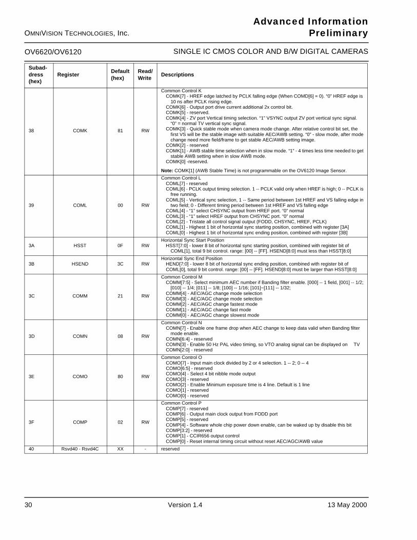
38 COMK 81 RW
Common Control KCOMK[7] - HREF edge latched by PCLK falling edge (When COMD[6] = 0). “0” HREF edge is
10 ns after PCLK rising edge. COMK[6] - Output port drive current additional 2x control bit.COMK[5] - reserved.COMK[4] - ZV port Vertical timing selection. “1” VSYNC output ZV port vertical sync signal.
“0” = normal TV vertical sync signal.COMK[3] - Quick stable mode when camera mode change. After relative control bit set, the
first VS will be the stable image with suitable AEC/AWB setting. “0” - slow mode, after modechange need more field/frame to get stable AEC/AWB setting image.
COMK[2] - reservedCOMK[1] - AWB stable time selection when in slow mode. “1” - 4 times less time needed to get
stable AWB setting when in slow AWB mode.COMK[0] -reserved.
Note: COMK[1] (AWB Stable Time) is not programmable on the OV6120 Image Sensor.
39 COML 00 RW
Common Control LCOML[7] - reservedCOML[6] - PCLK output timing selection. 1 -- PCLK valid only when HREF is high; 0 -- PCLK is
free running.COML[5] - Vertical sync selection, 1 -- Same period between 1st HREF and VS falling edge in
two field; 0 - Different timing period between 1st HREF and VS falling edgeCOML[4] - “1” select CHSYNC output from HREF port. “0” normalCOML[3] - “1” select HREF output from CHSYNC port. “0” normalCOML[2] - Tristate all control signal output (FODD, CHSYNC, HREF, PCLK)COML[1] - Highest 1 bit of horizontal sync starting position, combined with register [3A]COML[0] - Highest 1 bit of horizontal sync ending position, combined with register [3B]
3A HSST 0F RWHorizontal Sync Start Position
HSST[7:0] - lower 8 bit of horizontal sync starting position, combined with register bit ofCOML[1], total 9 bit control. range: [00] -- [FF]. HSEND[8:0] must less than HSST[8:0]
3B HSEND 3C RWHorizontal Sync End Position
HEND[7:0] - lower 8 bit of horizontal sync ending position, combined with register bit of COML[0], total 9 bit control. range: [00] -- [FF]. HSEND[8:0] must be larger than HSST[8:0]
3C COMM 21 RW
Common Control MCOMM[7:5] - Select minimum AEC number if Banding filter enable. [000] -- 1 field, [001] -- 1/2;
[010] -- 1/4; [011] -- 1/8; [100] -- 1/16; [101]~[111] -- 1/32; COMM[4] - AEC/AGC change mode selectionCOMM[3] - AEC/AGC change mode selectionCOMM[2] - AEC/AGC change fastest modeCOMM[1] - AEC/AGC change fast modeCOMM[0] - AEC/AGC change slowest mode
3D COMN 08 RW
Common Control NCOMN[7] - Enable one frame drop when AEC change to keep data valid when Banding filter
mode enable.COMN[6:4] - reservedCOMN[3] - Enable 50 Hz PAL video timing, so VTO analog signal can be displayed on TVCOMN[2:0] - reserved
3E COMO 80 RW
Common Control OCOMO[7] - Input main clock divided by 2 or 4 selection. 1 -- 2; 0 -- 4COMO[6:5] - reservedCOMO[4] - Select 4 bit nibble mode outputCOMO[3] - reservedCOMO[2] - Enable Minimum exposure time is 4 line. Default is 1 lineCOMO[1] - reservedCOMO[0] - reserved
3F COMP 02 RW
Common Control PCOMP[7] - reservedCOMP[6] - Output main clock output from FODD portCOMP[5] - reservedCOMP[4] - Software whole chip power down enable, can be waked up by disable this bitCOMP[3:2] - reservedCOMP[1] - CCIR656 output controlCOMP[0] - Reset internal timing circuit without reset AEC/AGC/AWB value
40 Rsvd40 - Rsvd4C XX - reserved
Subad-dress(hex)
RegisterDefault (hex)
Read/Write
Descriptions

13 May 2000 Version 1.4 31
OV6620/OV6120 SINGLE IC CMOS COLOR AND B/W DIGITAL CAMERAS
OMNIVISION TECHNOLOGIES, Inc.
Advanced InformationPreliminary
4D YMXA 02 RW
YUV Matrix Control (Main)YMXA[7:5] - reservedYMXA[4:3] - YUV/YCrCB selection:
[00] U = u, V = v[01] U = 0.938u, V = 0.838v[10] U = 0.563u, V = 0.714v[11] U = 0.5u, V = 0.877v
YMXA[2:0] - Reserved
Note: This function is not available on the OV6120 Image Sensor.
4E ARL A0 RW
AEC/AGC Reference LevelARL[7:5] - Reference Level Voltage Selection (Higher voltage = brighter final stable image)
[000] = 1.3v[001] = 1.5v[010] = 1.6v[011] = 1.7v[100] = 1.8v[101] = 1.9v[110] = 2.0v[111] = 2.1v
ARL[4:0] - Reserved
4F YMXB 00 RW
YUV Matrix Control (Secondary)YMXB[7:6] - Y channel delay selection: 0 ~ 3 tpYMXB[5:4] - UV delay selection: 0 ~ 6 tp YMXB[3:2] - Select UV average mode. [00] & [10]: U0/V0 (no delay); [01] -- 3 point average;
[11] -- 5 point average modeYMXB[1:0] - Color killer control: [00]:2.4v;[01]:2.6v;[10]:2.8v;[11]:3.0v
Note: This function is not available on the OV6120 Image Sensor.
50 Rsvd50 - Rsvd53 XX - reserved
Subad-dress(hex)
RegisterDefault (hex)
Read/Write
Descriptions