ADV7170/ADV7171 Digital PAL/NTSC Video Encoder with … · SSAF™ and Advanced Power Management...
64
Digital PAL/NTSC Video Encoder with 10-Bit SSAF™ and Advanced Power Management ADV7170/ADV7171 Rev. C Information furnished by Analog Devices is believed to be accurate and reliable. However, no responsibility is assumed by Analog Devices for its use, nor for any infringements of patents or other rights of third parties that may result from its use. Specifications subject to change without notice. No license is granted by implication or otherwise under any patent or patent rights of Analog Devices. Trademarks and registered trademarks are the property of their respective companies. One Technology Way, P.O. Box 9106, Norwood, MA 02062-9106, U.S.A. Tel: 781.329.4700 www.analog.com Fax: 781.461.3113 ©2002–2009 Analog Devices, Inc. All rights reserved. FEATURES ITU-R 1 BT601/656 YCrCb to PAL/NTSC video encoder High quality 10-bit video DACs SSAF (super sub-alias filter) Advanced power management features CGMS (copy generation management system) WSS (wide screen signalling) Simultaneous Y, U, V, C output format NTSC M, PAL M/N 2 , PAL B/D/G/H/I, PAL60 Single 27 MHz clock required (×2 oversampling) 80 dB video SNR 32-bit direct digital synthesizer for color subcarrier Multistandard video output support Composite (CVBS) Components S-Video (Y/C), YUV, and RGB EuroSCART output (RGB + CVBS/LUMA) Component YUV + CHROMA Video input data port supports CCIR-656 4:2:2 8-bit parallel input format 4:2:2 16-bit parallel input format Programmable simultaneous composite and S-Video or RGB (SCART)/YUV video outputs Programmable luma filters (low-pass [PAL/NTSC]) notch, extended (SSAF, CIF, and QCIF) Programmable chroma filters (low-pass [0.65 MHz, 1.0 MHz, 1.2 MHz and 2.0 MHz], CIF and QCIF) Programmable VBI (vertical blanking interval) Programmable subcarrier frequency and phase Programmable LUMA delay Individual on/off control of each DAC CCIR and square pixel operation Integrated subcarrier locking to external video source Color signal control/burst signal control Interlaced/noninterlaced operation Complete on-chip video timing generator Programmable multimode master/slave operation Macrovision® AntiTaping Rev. 7.1 (ADV7170 only) 3 Closed captioning support Teletext insertion port (PAL-WST) On-board color bar generation On-board voltage reference 2-wire serial MPU interface (I 2 C®-compatible and Fast I 2 C) Single supply 5 V or 3.3 V operation Small 44-lead MQFP/TQFP packages Industrial temperature grade = −40°C to +85°C 4 APPLICATIONS High performance DVD playback systems, portable video equipment including digital still cameras and laptop PCs, video games, PC video/multimedia and digital satellite/cable systems (set-top boxes/IRD) 1 ITU-R and CCIR are used interchangeably in this document (ITU-R has replaced CCIR recommendations). 2 Throughout the document N is referenced to PAL- Combination -N. 3 Protected by U.S. Patents 4,631,603;, 4,577,216, 4,819,098; and other intellectual property rights. The Macrovision anticopy process is licensed for noncommercial home use only, which is its sole intended use in the device. Please contact sales office for latest Macrovision version available. 4 Refer to Table 8 for complete operating details. 10-BIT DAC 10 10-BIT DAC 10 10-BIT DAC 10 10 10-BIT DAC 10 10 10 M U L T I P L E X E R DAC D (PIN 27) DAC C (PIN 26) DAC B (PIN 31) DAC A (PIN 32) V REF R SET COMP VOLTAGE REFERENCE CIRCUIT ADV7170/ADV7171 GND SCRESET/RTC ALSB TTXREQ TTX SDATA SCLOCK CLOCK REAL-TIME CONTROL CIRCUIT I 2 C MPU PORT VIDEO TIMING GENERATOR 4:2:2 TO 4:4:4 INTER- POLATOR 8 V 8 U 8 Y 8 8 8 8 8 9 8 8 9 YCrCb TO YUV MATRIX ADD BURST ADD SYNC POWER MANAGEMENT CONTROL (SLEEP MODE) V AA RESET COLOR DATA P7–P0 P15–P8 HSYNC BLANK FIELD/VSYNC INTER- POLATOR INTER- POLATOR PROGRAMMABLE LUMINANCE FILTER PROGRAMMABLE CHROMINANCE FILTER CGMS AND WSS INSERTION BLOCK TELETEXT INSERTION BLOCK 10 10 10 U V 10 10 SIN/COS DDS BLOCK YUV TO RGB MATRIX 00221-001 Figure 1. Functional Block Diagram Protected by U.S. Patents 5,343,196; 5,442,355; and other intellectual property rights.
Transcript of ADV7170/ADV7171 Digital PAL/NTSC Video Encoder with … · SSAF™ and Advanced Power Management...

Digital PAL/NTSC Video Encoder with 10-BitSSAF™ and Advanced Power Management
ADV7170/ADV7171
Rev. C Information furnished by Analog Devices is believed to be accurate and reliable. However, no responsibility is assumed by Analog Devices for its use, nor for any infringements of patents or other rights of third parties that may result from its use. Specifications subject to change without notice. No license is granted by implication or otherwise under any patent or patent rights of Analog Devices. Trademarks and registered trademarks are the property of their respective companies.
One Technology Way, P.O. Box 9106, Norwood, MA 02062-9106, U.S.A. Tel: 781.329.4700 www.analog.com Fax: 781.461.3113 ©2002–2009 Analog Devices, Inc. All rights reserved.
FEATURES ITU-R1 BT601/656 YCrCb to PAL/NTSC video encoder High quality 10-bit video DACs SSAF (super sub-alias filter) Advanced power management features CGMS (copy generation management system) WSS (wide screen signalling) Simultaneous Y, U, V, C output format NTSC M, PAL M/N2, PAL B/D/G/H/I, PAL60 Single 27 MHz clock required (×2 oversampling) 80 dB video SNR 32-bit direct digital synthesizer for color subcarrier Multistandard video output support
Composite (CVBS) Components S-Video (Y/C), YUV, and RGB EuroSCART output (RGB + CVBS/LUMA) Component YUV + CHROMA
Video input data port supports CCIR-656 4:2:2 8-bit parallel input format 4:2:2 16-bit parallel input format
Programmable simultaneous composite and S-Video or RGB (SCART)/YUV video outputs
Programmable luma filters (low-pass [PAL/NTSC]) notch, extended (SSAF, CIF, and QCIF)
Programmable chroma filters (low-pass [0.65 MHz, 1.0 MHz, 1.2 MHz and 2.0 MHz], CIF and QCIF)
Programmable VBI (vertical blanking interval) Programmable subcarrier frequency and phase
Programmable LUMA delay Individual on/off control of each DAC CCIR and square pixel operation Integrated subcarrier locking to external video source Color signal control/burst signal control Interlaced/noninterlaced operation Complete on-chip video timing generator Programmable multimode master/slave operation Macrovision® AntiTaping Rev. 7.1 (ADV7170 only)3 Closed captioning support Teletext insertion port (PAL-WST) On-board color bar generation On-board voltage reference 2-wire serial MPU interface (I2C®-compatible and Fast I2C) Single supply 5 V or 3.3 V operation Small 44-lead MQFP/TQFP packages Industrial temperature grade = −40°C to +85°C4
APPLICATIONS High performance DVD playback systems, portable video
equipment including digital still cameras and laptop PCs, video games, PC video/multimedia and digital satellite/cable systems (set-top boxes/IRD)
1 ITU-R and CCIR are used interchangeably in this document (ITU-R has replaced CCIR recommendations).
2 Throughout the document N is referenced to PAL- Combination -N. 3 Protected by U.S. Patents 4,631,603;, 4,577,216, 4,819,098; and other intellectual
property rights. The Macrovision anticopy process is licensed for noncommercial home use only, which is its sole intended use in the device. Please contact sales office for latest Macrovision version available.
4 Refer to Table 8 for complete operating details.
10-BITDAC
10
10-BITDAC
10
10-BITDAC
10
10 10-BITDAC
10
10
10
MULTIPLEXER
DAC D (PIN 27)
DAC C (PIN 26)
DAC B (PIN 31)
DAC A (PIN 32)
VREFRSETCOMP
VOLTAGEREFERENCE
CIRCUIT
ADV7170/ADV7171
GNDSCRESET/RTCALSB
TTXREQ TTX
SDATASCLOCKCLOCK
REAL-TIMECONTROLCIRCUIT
I2C MPU PORTVIDEO TIMINGGENERATOR
4:2:2 TO4:4:4
INTER-POLATOR 8 V
8U
8 Y
8
8
8
8
8
9
8
8
9
YCrCbTO
YUVMATRIX ADD
BURST
ADDSYNC
POWERMANAGEMENT
CONTROL(SLEEP MODE)VAA
RESETCOLOR
DATAP7–P0
P15–P8
HSYNC
BLANKFIELD/VSYNC
INTER-POLATOR
INTER-POLATOR
PROGRAMMABLELUMINANCE
FILTER
PROGRAMMABLECHROMINANCE
FILTER
CGMS AND WSSINSERTION
BLOCK
TELETEXTINSERTION
BLOCK
10
10
10 U
V
1010
SIN/COSDDS BLOCK
YUV TORGB
MATRIX00
221-
001
Figure 1. Functional Block Diagram
Protected by U.S. Patents 5,343,196; 5,442,355; and other intellectual property rights.
ADV7170/ADV7171
Rev. C | Page 2 of 64
TABLE OF CONTENTS Specifications ..................................................................................... 4
Dynamic Specifications ............................................................... 6
Timing Specifications .................................................................. 7
Timing Diagrams.......................................................................... 9
Absolute Maximum Ratings .......................................................... 10
Package Thermal Performance ................................................. 10
ESD Caution ................................................................................ 10
Pin Configuration and Function Descriptions ........................... 11
General Description ....................................................................... 13
Data Path Description ................................................................ 13
Internal Filter Response ............................................................. 14
Typical Performance Characteristics ........................................... 15
Features ............................................................................................ 18
Color Bar Generation ................................................................ 18
Square Pixel Mode ...................................................................... 18
Color Signal Control .................................................................. 18
Burst Signal Control ................................................................... 18
NTSC Pedestal Control ............................................................. 18
Pixel Timing Description .......................................................... 18
Subcarrier Reset .......................................................................... 18
Real-Time Control ..................................................................... 18
Video Timing Description ........................................................ 18
Power-On Reset .......................................................................... 26
SCH Phase Mode ........................................................................ 26
MPU Port Description ............................................................... 26
Register Accesses ........................................................................ 27
Register Programming ................................................................... 28
Subaddress Register (SR7 to SR0) ............................................ 28
Register Select (SR5 to SR0) ...................................................... 28
Mode Register 0 MR0 (MR07 to MR00) ................................. 28
MR0 Bit Description .................................................................. 28
Mode Register 1 MR1 (MR17 to MR10) ................................. 30
MR1 Bit Description .................................................................. 30
Mode Register 2 MR2 (MR27 to MR20) ................................. 30
MR2 Bit Description .................................................................. 30
Mode Register 3 MR3 (MR37 to MR30) .................................... 32
MR3 Bit Description .................................................................... 32
Mode Register 4 MR4 (MR47 to MR40) ................................. 33
MR4 Bit Description .................................................................. 33
VSYNC_3H (MR43) .................................................................. 33
Timing Mode Register 0 (TR07 to TR00) ............................... 33
TR0 Bit Description ................................................................... 34
Timing Mode Register 1 (TR17 to TR10) ............................... 34
TR1 Bit Description ................................................................... 34
Subcarrier Frequency Registers 0 to 3 (FSC3 to FSC0) ......... 35
Subcarrier Phase Registers (FP7 to FP0) ................................. 35
Closed Captioning Even Field Data Register 1 to 0 (CED15 to CED0) .......................................................................................... 35
Closed Captioning Odd Field Data Registers 1 to 0 (CCD15 to CCD0) ..................................................................................... 35
NTSC Pedestal/PAL Teletext Control Registers 3 to 0 (PCE15 to PCE0, PCO15 to PCO0)/(TXE15 to TXE0, TXO15 to TXO0) .......................................................................................... 36
Teletext Request Control Register TC07 (TC07 to TC00) .... 36
CGMS_WSS Register 0 C/W0 (C/W07 to C/W00) .............. 36
C/W0 Bit Description ................................................................ 36
CGMS_WSS Register 1 C/W1 (C/W17 to C/W10) .............. 37
C/W1 Bit Description ................................................................ 37
CGMS Data Bits (C/W17 to C/W16) ...................................... 37
CGMS_WSS Register 2 C/W1 (C/W27 to C/W20) .............. 37
C/W2 Bit Description ................................................................ 37
Appendices ...................................................................................... 38
Appendix 1—Board Design and Layout Considerations...... 38
ADV7170/ADV7171
Rev. C | Page 3 of 64
Appendix 2—Closed Captioning .............................................. 40
Appendix 3—Copy Generation Management System (CGMS) ........................................................................................ 41
Appendix 4—Wide Screen Signaling ....................................... 42
Appendix 5—Teletext Insertion ................................................ 43
Appendix 6—Waveforms ........................................................... 44
Appendix 7—Optional Output Filter ....................................... 48
Appendix 8—Optional DAC Buffering ................................... 48
Appendix 9—Recommended Register Values ........................ 49
Appendix 10—Output Waveforms ........................................... 51
Outline Dimensions ........................................................................ 61
Ordering Guide ........................................................................... 62
REVISION HISTORY
3/09—Rev. B to Rev. C
Changes to Table 8 .......................................................................... 10 Updated Outline Dimensions ........................................................ 61 Added Figure 103, Renumbered Figures Sequentially ............... 61 Changes to Ordering Guide ........................................................... 61
6/05—Rev. A to Rev. B Updated Format .................................................................. Universal Changes to Features Section ............................................................ 1 Changes to Table 8 .......................................................................... 10 Changes to Square Pixel Mode Section ........................................ 18 Changes to Figure 37 ...................................................................... 29 Changes to Figure 42 ...................................................................... 33 Changes to Subcarrier Frequency Registers 3 to 0 Section ....... 35 Changes to Figure 45 ...................................................................... 35 Changes to Figure 82 ...................................................................... 48 Changes to Ordering Guide ........................................................... 62
6/02—Starting Rev. A to Rev. B Changes to Specifications ................................................................. 3 Changes to Package Thermal Performance section...9
ADV7170/ADV7171
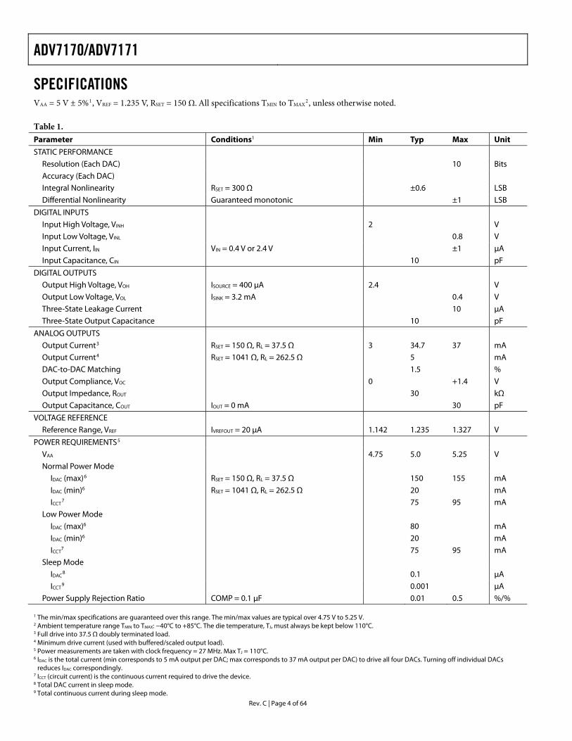
Rev. C | Page 4 of 64
SPECIFICATIONS VAA = 5 V ± 5%1, VREF = 1.235 V, RSET = 150 Ω. All specifications TMIN to TMAX
2, unless otherwise noted.
Table 1. Parameter Conditions1 Min Typ Max Unit STATIC PERFORMANCE
Resolution (Each DAC) 10 Bits Accuracy (Each DAC) Integral Nonlinearity RSET = 300 Ω ±0.6 LSB Differential Nonlinearity Guaranteed monotonic ±1 LSB
DIGITAL INPUTS Input High Voltage, VINH 2 V Input Low Voltage, VINL 0.8 V Input Current, IIN VIN = 0.4 V or 2.4 V ±1 μA Input Capacitance, CIN 10 pF
DIGITAL OUTPUTS Output High Voltage, VOH ISOURCE = 400 μA 2.4 V Output Low Voltage, VOL ISINK = 3.2 mA 0.4 V Three-State Leakage Current 10 μA Three-State Output Capacitance 10 pF
ANALOG OUTPUTS Output Current3 RSET = 150 Ω, RL = 37.5 Ω 3 34.7 37 mA Output Current4 RSET = 1041 Ω, RL = 262.5 Ω 5 mA DAC-to-DAC Matching 1.5 % Output Compliance, VOC 0 +1.4 V Output Impedance, ROUT 30 kΩ Output Capacitance, COUT IOUT = 0 mA 30 pF
VOLTAGE REFERENCE Reference Range, VREF IVREFOUT = 20 μA 1.142 1.235 1.327 V
POWER REQUIREMENTS5 VAA 4.75 5.0 5.25 V Normal Power Mode
IDAC (max)6 RSET = 150 Ω, RL = 37.5 Ω 150 155 mA IDAC (min)6 RSET = 1041 Ω, RL = 262.5 Ω 20 mA ICCT
7 75 95 mA Low Power Mode
IDAC (max)6 80 mA IDAC (min)6 20 mA ICCT
7 75 95 mA
Sleep Mode IDAC
8 0.1 μA ICCT
9 0.001 μA Power Supply Rejection Ratio COMP = 0.1 μF 0.01 0.5 %/%
1 The min/max specifications are guaranteed over this range. The min/max values are typical over 4.75 V to 5.25 V. 2 Ambient temperature range TMIN to TMAX: −40°C to +85°C. The die temperature, TJ, must always be kept below 110°C. 3 Full drive into 37.5 Ω doubly terminated load. 4 Minimum drive current (used with buffered/scaled output load). 5 Power measurements are taken with clock frequency = 27 MHz. Max TJ = 110°C. 6 IDAC is the total current (min corresponds to 5 mA output per DAC; max corresponds to 37 mA output per DAC) to drive all four DACs. Turning off individual DACs
reduces IDAC correspondingly. 7 ICCT (circuit current) is the continuous current required to drive the device. 8 Total DAC current in sleep mode. 9 Total continuous current during sleep mode.
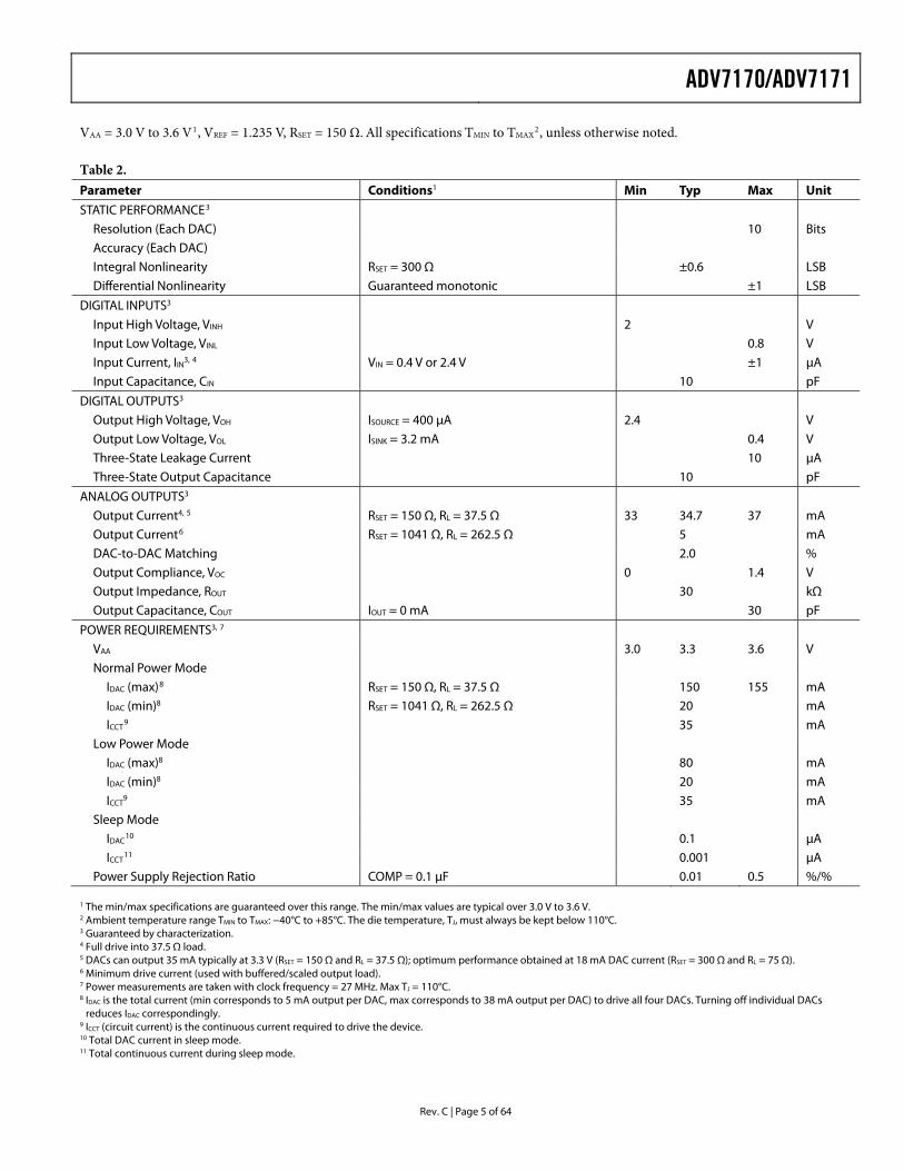
ADV7170/ADV7171
Rev. C | Page 5 of 64
VAA = 3.0 V to 3.6 V1, VREF = 1.235 V, RSET = 150 Ω. All specifications TMIN to TMAX2, unless otherwise noted.
Table 2. Parameter Conditions1 Min Typ Max Unit STATIC PERFORMANCE3
Resolution (Each DAC) 10 Bits Accuracy (Each DAC) Integral Nonlinearity RSET = 300 Ω ±0.6 LSB Differential Nonlinearity Guaranteed monotonic ±1 LSB
DIGITAL INPUTS3
Input High Voltage, VINH 2 V Input Low Voltage, VINL 0.8 V Input Current, IIN
3, 4 VIN = 0.4 V or 2.4 V ±1 μA
Input Capacitance, CIN 10 pF DIGITAL OUTPUTS3
Output High Voltage, VOH ISOURCE = 400 μA 2.4 V Output Low Voltage, VOL ISINK = 3.2 mA 0.4 V Three-State Leakage Current 10 μA Three-State Output Capacitance 10 pF
ANALOG OUTPUTS3
Output Current4, 5 RSET = 150 Ω, RL = 37.5 Ω 33 34.7 37 mA
Output Current6 RSET = 1041 Ω, RL = 262.5 Ω 5 mA DAC-to-DAC Matching 2.0 % Output Compliance, VOC 0 1.4 V Output Impedance, ROUT 30 kΩ Output Capacitance, COUT IOUT = 0 mA 30 pF
POWER REQUIREMENTS3, 7
VAA 3.0 3.3 3.6 V Normal Power Mode
IDAC (max)8 RSET = 150 Ω, RL = 37.5 Ω 150 155 mA IDAC (min)8 RSET = 1041 Ω, RL = 262.5 Ω 20 mA ICCT
9 35 mA Low Power Mode
IDAC (max)8 80 mA IDAC (min)8 20 mA ICCT
9 35 mA
Sleep Mode IDAC
10 0.1 μA ICCT
11 0.001 μA Power Supply Rejection Ratio COMP = 0.1 μF 0.01 0.5 %/%
1 The min/max specifications are guaranteed over this range. The min/max values are typical over 3.0 V to 3.6 V. 2 Ambient temperature range TMIN to TMAX: −40°C to +85°C. The die temperature, TJ, must always be kept below 110°C. 3 Guaranteed by characterization. 4 Full drive into 37.5 Ω load. 5 DACs can output 35 mA typically at 3.3 V (RSET = 150 Ω and RL = 37.5 Ω); optimum performance obtained at 18 mA DAC current (RSET = 300 Ω and RL = 75 Ω). 6 Minimum drive current (used with buffered/scaled output load). 7 Power measurements are taken with clock frequency = 27 MHz. Max TJ = 110°C. 8 IDAC is the total current (min corresponds to 5 mA output per DAC, max corresponds to 38 mA output per DAC) to drive all four DACs. Turning off individual DACs
reduces IDAC correspondingly. 9 ICCT (circuit current) is the continuous current required to drive the device. 10 Total DAC current in sleep mode. 11 Total continuous current during sleep mode.

ADV7170/ADV7171
Rev. C | Page 6 of 64
DYNAMIC SPECIFICATIONS VAA = 5 V ± 5%1, VREF = 1.235 V, RSET = 150 Ω. All specifications TMIN to TMAX
2, unless otherwise noted.
Table 3. Parameter Conditions1 Min Typ Max Unit Differential Gain3, 4
Normal power mode 0.3 0.7 % Differential Phase3, 4
Normal power mode 0.4 0.7 Degrees Differential Gain3, 4
Lower power mode 1.0 2.0 % Differential Phase3, 4
Lower power mode 1.0 2.0 Degrees SNR3, 4(Pedestal) RMS 80 dB rms SNR3, 4(Pedestal) Peak periodic 70 dB p-p SNR3, 4(Ramp) RMS 60 dB rms SNR3, 4(Ramp) Peak periodic 58 dB p-p Hue Accuracy3, 4
0.7 1.2 Degrees Color Saturation Accuracy3, 4
0.9 1.4 % Chroma Nonlinear Gain3, 4
Referenced to 40 IRE 0.6 ±% Chroma Nonlinear Phase3 4
0.3 0.5 ±Degrees Chroma/Luma Intermod3, 4
0.2 0.4 ±% Chroma/Luma Gain Inequality3, 4
1.0 1.4 ±% Chroma/Luma Delay Inequality3, 4
0.5 2.0 ns Luminance Nonlinearity3, 4
0.8 1.4 ±% Chroma AM Noise3, 4
82 85 dB Chroma PM Noise3, 4
79 81 dB
1 The min/max specifications are guaranteed over this range. The min/max values are typical over 4.75 V to 5.25 V. 2 Ambient temperature range TMIN to TMAX: −40°C to +85°C. The die temperature, TJ, must always be kept below 110°C. 3 Guaranteed by characterization. 4 These specifications are for the low-pass filter only and are guaranteed by design.
VAA = 3.0 V to 3.6 V1, VREF = 1.235 V, RSET = 150 Ω. All specifications TMIN to TMAX2, unless otherwise noted.
Table 4. Parameter Conditions1 Min Typ Max Unit Differential Gain3 Normal power mode 1.0 % Differential Phase3
Normal power mode 0.5 Degrees Differential Gain3
Lower power mode 0.6 % Differential Phase3
Lower power mode 0.5 Degrees SNR3 (Pedestal) RMS 78 dB rms SNR3 (Pedestal) Peak periodic 70 dB p-p SNR3 (Ramp) RMS 60 dB rms SNR3 (Ramp) Peak periodic 58 dB p-p Hue Accuracy3
1.0 Degrees Color Saturation Accuracy3
1.0 % Luminance Nonlinearity3, 4
1.4 ±% Chroma AM Noise3, 4
80 dB Chroma PM Noise3, 4
79 dB Chroma Nonlinear Gain3, 4
Referenced to 40 IRE 0.6 ±% Chroma Nonlinear Phase3, 4
0.3 0.5 ±Degrees Chroma/Luma Intermod3, 4
0.2 0.4 ±%
1 The min/max specifications are guaranteed over this range. The min/max values are typical over 4.75 V to 5.25 V. 2 Ambient temperature range TMIN to TMAX: −40°C to +85°C. The die temperature, TJ, must always be kept below 110°C. 3 Guaranteed by characterization. 4 These specifications are for the low-pass filter only and are guaranteed by design. For other internal filters, see Table 10.
ADV7170/ADV7171
Rev. C | Page 7 of 64
TIMING SPECIFICATIONS VAA = 4.75 V to 5.25 V1, VREF = 1.235 V, RSET = 150 Ω. All specifications TMIN to TMAX
2, unless otherwise noted.
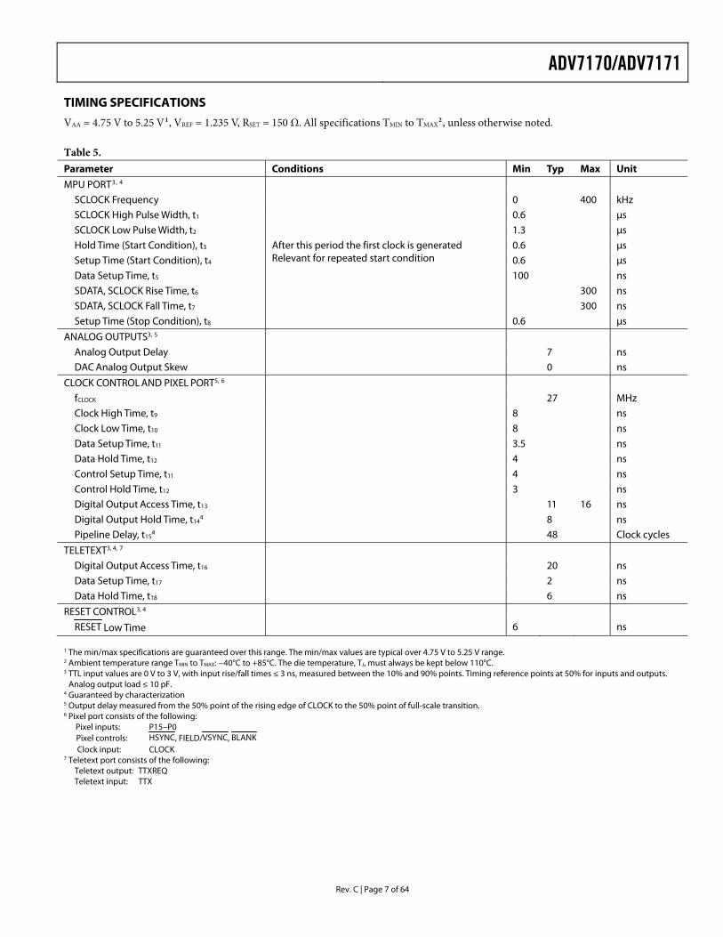
Table 5. Parameter Conditions Min Typ Max Unit MPU PORT3, 4
SCLOCK Frequency 0 400 kHz SCLOCK High Pulse Width, t1 0.6 μs SCLOCK Low Pulse Width, t2 1.3 μs Hold Time (Start Condition), t3 After this period the first clock is generated
Relevant for repeated start condition 0.6 μs
Setup Time (Start Condition), t4 0.6 μs Data Setup Time, t5 100 ns SDATA, SCLOCK Rise Time, t6 300 ns SDATA, SCLOCK Fall Time, t7 300 ns Setup Time (Stop Condition), t8 0.6 μs
ANALOG OUTPUTS3, 5
Analog Output Delay 7 ns DAC Analog Output Skew 0 ns
CLOCK CONTROL AND PIXEL PORT5, 6
fCLOCK 27 MHz Clock High Time, t9 8 ns Clock Low Time, t10 8 ns Data Setup Time, t11 3.5 ns Data Hold Time, t12 4 ns Control Setup Time, t11 4 ns Control Hold Time, t12 3 ns Digital Output Access Time, t13 11 16 ns Digital Output Hold Time, t14
4 8 ns
Pipeline Delay, t154
48 Clock cycles TELETEXT3, 4, 7
Digital Output Access Time, t16 20 ns Data Setup Time, t17 2 ns Data Hold Time, t18 6 ns
RESET CONTROL3, 4
RESET Low Time 6 ns
1 The min/max specifications are guaranteed over this range. The min/max values are typical over 4.75 V to 5.25 V range. 2 Ambient temperature range TMIN to TMAX: −40°C to +85°C. The die temperature, TJ, must always be kept below 110°C. 3 TTL input values are 0 V to 3 V, with input rise/fall times ≤ 3 ns, measured between the 10% and 90% points. Timing reference points at 50% for inputs and outputs.
Analog output load ≤ 10 pF. 4 Guaranteed by characterization 5 Output delay measured from the 50% point of the rising edge of CLOCK to the 50% point of full-scale transition. 6 Pixel port consists of the following:
Pixel inputs: P15–P0 Pixel controls: HSYNC, FIELD/VSYNC, BLANK Clock input: CLOCK
7 Teletext port consists of the following: Teletext output: TTXREQ Teletext input: TTX
ADV7170/ADV7171
Rev. C | Page 8 of 64
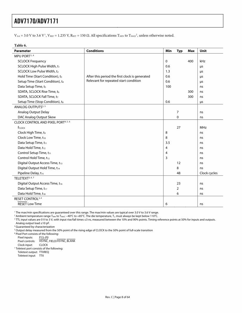
VAA = 3.0 V to 3.6 V1, VREF = 1.235 V, RSET = 150 Ω. All specifications TMIN to TMAX2, unless otherwise noted.
Table 6. Parameter Conditions Min Typ Max Unit MPU PORT3, 4
SCLOCK Frequency 0 400 kHz SCLOCK High Pulse Width, t1 0.6 μs SCLOCK Low Pulse Width, t2 1.3 μs Hold Time (Start Condition), t3 After this period the first clock is generated
Relevant for repeated start condition 0.6 μs
Setup Time (Start Condition), t4 0.6 μs Data Setup Time, t5 100 ns SDATA, SCLOCK Rise Time, t6 300 ns SDATA, SCLOCK Fall Time, t7 300 ns Setup Time (Stop Condition), t8 0.6 μs
ANALOG OUTPUTS3, 5
Analog Output Delay 7 ns DAC Analog Output Skew 0 ns
CLOCK CONTROL AND PIXEL PORT4, 5, 6
fCLOCK 27 MHz Clock High Time, t9 8 ns Clock Low Time, t10 8 ns Data Setup Time, t11 3.5 ns Data Hold Time, t12 4 ns Control Setup Time, t11 4 ns Control Hold Time, t12 3 ns Digital Output Access Time, t13 12 ns Digital Output Hold Time, t14 8 ns Pipeline Delay, t15 48 Clock cycles
TELETEXT3, 4, 7
Digital Output Access Time, t16 23 ns Data Setup Time, t17 2 ns Data Hold Time, t18 6 ns
RESET CONTROL3, 4
RESET Low Time 6 ns
1 The max/min specifications are guaranteed over this range. The max/min values are typical over 3.0 V to 3.6 V range. 2 Ambient temperature range TMIN to TMAX: −40°C to +85°C. The die temperature, TJ, must always be kept below 110°C. 3 TTL input values are 0 V to 3 V, with input rise/fall times ≤3 ns, measured between the 10% and 90% points. Timing reference points at 50% for inputs and outputs.
Analog output load ≤10 pF. 4 Guaranteed by characterization 5 Output delay measured from the 50% point of the rising edge of CLOCK to the 50% point of full-scale transition 6 Pixel Port consists of the following:
Pixel inputs: P15–P0 Pixel controls: HSYNC, FIELD/VSYNC, BLANK Clock input: CLOCK
7 Teletext port consists of the following: Teletext output: TTXREQ Teletext input: TTX
ADV7170/ADV7171
Rev. C | Page 9 of 64
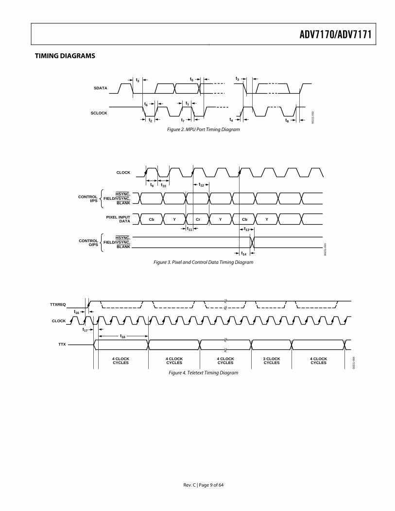
TIMING DIAGRAMS
t3
t1t6
t2 t7
t5
SDATA
SCLOCK
t3
t4 t8 0022
1-00
2
Figure 2. MPU Port Timing Diagram
t9
t11
CLOCK
PIXEL INPUTDATA
t10 t12
HSYNC,FIELD/VSYNC,
BLANK
Cb Y Cr Y Cb Y
HSYNC,FIELD/VSYNC,
BLANKt14
CONTROLI/PS
CONTROLO/PS
t13
0022
1-00
3
Figure 3. Pixel and Control Data Timing Diagram
t16
t17t18
TTXREQ
CLOCK
TTX
4 CLOCKCYCLES
4 CLOCKCYCLES
4 CLOCKCYCLES
3 CLOCKCYCLES
4 CLOCKCYCLES
0022
1-00
4
Figure 4. Teletext Timing Diagram

ADV7170/ADV7171
Rev. C | Page 10 of 64
ABSOLUTE MAXIMUM RATINGS
Table 7. Parameter Rating VAA to GND 7 V Voltage on Any Digital Input Pin GND − 0.5 V to VAA + 0.5 V Storage Temperature (TS) −65°C to +150°C Junction Temperature (TJ) 150°C Lead Temperature (Soldering, 10 sec) 260°C Analog Outputs to GND1 GND − 0.5 V to VAA
1 Analog output short circuit to any power supply or GND can be of an indefinite duration.
Stresses above those listed under Absolute Maximum Ratings may cause permanent damage to the device. This is a stress rating only; functional operation of the device at these or any other conditions above those indicated in the operational sections of this specification is not implied. Exposure to absolute maximum rating conditions for extended periods may affect device reliability. Only one absolute maximum rating may be applied at any one time.
PACKAGE THERMAL PERFORMANCE The 44-MQFP package used for this device takes advantage of an ADI patented thermal coastline lead frame construction. This maximizes heat transfer into the leads and reduces the package thermal resistance.
For the MQFP package, the junction-to-ambient (θJA) thermal resistance in still air on a four-layer PCB is 35.5°C/W. The junction-to-case thermal resistance (θJC) is 13.75°C/W. For the TQFP package, θJA in still air on a four-layer PCB is 53.2°C/W. θJC is 11.1°C/W. Junction Temperature = TJ = [VAA (Σ DAC Output Current + ICCT) × θJA] + Ambient Temperature.
Table 8. Allowable Operating Conditions for KS and KSU Package Options KS, WBS KSU Conditions 3 V 5 V 3 V 5 V 4 DAC ON Double 75R1 Yes +70°C max +70°C max No 4 DAC ON Low Power2 Yes Yes Yes No 4 DAC ON Buffering3 Yes Yes Yes Yes 3 DAC ON Double 75R Yes Yes Yes No 3 DAC ON Low Power Yes Yes Yes Yes 3 DAC ON Buffering Yes Yes Yes Yes Yes Yes Yes Yes Yes Yes Yes Yes 4 DAC ON Buffering Yes Yes
1 DAC ON Double 75R refers to a condition where the DACs are terminated in a double 75R load and low power mode is disabled.
2 DAC ON Low Power refers to a condition where the DACs are terminated in a double 75R load and low power mode is enabled.
3 DAC ON Buffering refers to a condition where the DAC current is reduced to 5 mA and external buffers are used to drive the video load.
ESD CAUTION ESD (electrostatic discharge) sensitive device. Electrostatic charges as high as 4000 V readily accumulate on the human body and test equipment and can discharge without detection. Although this product features proprietary ESD protection circuitry, permanent damage may occur on devices subjected to high energy electrostatic discharges. Therefore, proper ESD precautions are recommended to avoid performance degradation or loss of functionality.
ADV7170/ADV7171
Rev. C | Page 11 of 64
PIN CONFIGURATION AND FUNCTION DESCRIPTIONS
44
CLO
CK
43
GN
D
42
P4
41
P3
40
P2
39
P1
38
P0
37
TTX
36
TTXR
EQ
35
SCR
ESET
/RTC
34
RSE
T
32 DAC A31 DAC B30 VAA
27 DAC D
28 VAA
29 GND
33 VREF
26 DAC C25 COMP24 SDATA23 SCLOCK
2P53P64P7
7P10
6P9
5P8
1VAA
8P119P1210GND11VAA
12
P13
13
P14
14P1
515
HSY
NC
16
FIEL
D/V
SYN
C
17
BLA
NK
18
ALS
B
19
GN
D
20
V AA
21
GN
D
22
RES
ET
PIN 1
ADV7170/ADV7171MQFP/TQFP
TOP VIEW(Not to Scale)
0022
1-00
5
Figure 5. Pin Configuration
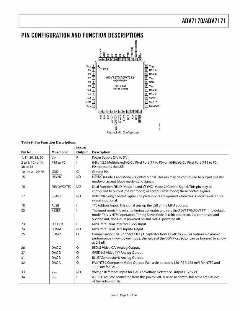
Table 9. Pin Function Descriptions
Pin No. Mnemonic Input/ Output Description
1, 11, 20, 28, 30 VAA P Power Supply (3 V to 5 V). 2 to 9, 12 to 14, 38 to 42
P15 to P0 I 8-Bit 4:2:2 Multiplexed YCrCb Pixel Port (P7 to P0) or 16-Bit YCrCb Pixel Port (P15 to P0). P0 represents the LSB.
10, 19, 21, 29, 43 GND G Ground Pin. 15 HSYNC
I/O HSYNC (Mode 1 and Mode 2) Control Signal. This pin may be configured to output (master
mode) or accept (slave mode) sync signals. 16 FIELD/VSYNC
I/O Dual Function FIELD (Mode 1) and VSYNC (Mode 2) Control Signal. This pin may be
configured to output (master mode) or accept (slave mode) these control signals. 17 BLANK
I/O Video Blanking Control Signal. The pixel inputs are ignored when this is Logic Level 0. This
signal is optional. 18 ALSB I TTL Address Input. This signal sets up the LSB of the MPU address. 22 RESET
I The input resets the on-chip timing generator and sets the ADV7170/ADV7171 into default
mode. This is NTSC operation, Timing Slave Mode 0, 8-bit operation, 2 × composite and S-Video out, and DAC B powered on and DAC D powered off.
23 SCLOCK I MPU Port Serial Interface Clock Input. 24 SDATA I/O MPU Port Serial Data Input/Output. 25 COMP O Compensation Pin. Connect a 0.1 μF capacitor from COMP to VAA. For optimum dynamic
performance in low power mode, the value of the COMP capacitor can be lowered to as low as 2.2 nF.
26 DAC C O RED/S-Video C/V Analog Output. 27 DAC D O GREEN/S-Video Y/Y Analog Output. 31 DAC B O BLUE/Composite/U Analog Output. 32 DAC A O PAL/NTSC Composite Video Output. Full-scale output is 180 IRE (1286 mV) for NTSC and
1300 mV for PAL. 33 VREF I/O Voltage Reference Input for DACs or Voltage Reference Output (1.235 V). 34 RSET I A 150 Ω resistor connected from this pin to GND is used to control full-scale amplitudes
of the video signals.
ADV7170/ADV7171
Rev. C | Page 12 of 64
Pin No. Mnemonic Input/ Output Description
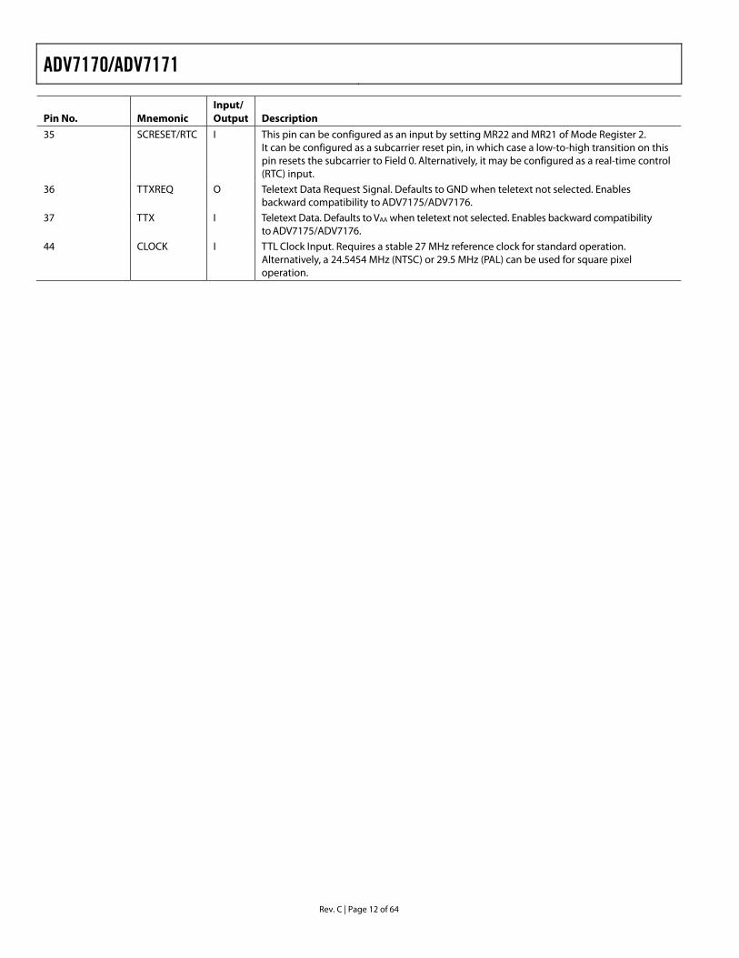
35 SCRESET/RTC I This pin can be configured as an input by setting MR22 and MR21 of Mode Register 2. It can be configured as a subcarrier reset pin, in which case a low-to-high transition on this pin resets the subcarrier to Field 0. Alternatively, it may be configured as a real-time control (RTC) input.
36 TTXREQ O Teletext Data Request Signal. Defaults to GND when teletext not selected. Enables backward compatibility to ADV7175/ADV7176.
37 TTX I Teletext Data. Defaults to VAA when teletext not selected. Enables backward compatibility to ADV7175/ADV7176.
44 CLOCK I TTL Clock Input. Requires a stable 27 MHz reference clock for standard operation. Alternatively, a 24.5454 MHz (NTSC) or 29.5 MHz (PAL) can be used for square pixel operation.
ADV7170/ADV7171
Rev. C | Page 13 of 64
GENERAL DESCRIPTION The ADV7170/ADV7171 are integrated digital video encoders that convert digital CCIR-601 4:2:2 8- or 16-bit component video data into a standard analog baseband television signal compatible with worldwide standards.
The on-board SSAF (super sub-alias filter) with extended luminance frequency response and sharp stop band attenuation enables studio-quality video playback on modern TVs, giving optimal horizontal line resolution.
An advanced power management circuit enables optimal control of power consumption in both normal operating modes and power-down or sleep modes.
The ADV7170/ADV7171 support both PAL and NTSC square pixel operation. The parts also incorporate WSS and CGMS-A data control generation.
The output video frames are synchronized with the incoming data timing reference codes. Optionally, the encoder accepts and can generate HSYNC, VSYNC, and FIELD timing signals. These timing signals can be adjusted to change pulse width and position while the part is in the master mode. The encoder requires a single, two-times pixel rate (27 MHz) clock for standard operation. Alternatively, the encoder requires a 24.5454 MHz clock for NTSC or 29.5 MHz clock for PAL square pixel mode operation. All internal timing is generated on-chip.
A separate teletext port enables the user to directly input teletext data during the vertical blanking interval.
The ADV7170/ADV7171 modes are set up over a 2-wire, serial bidirectional port (I2C-compatible) with two slave addresses.
Functionally, the ADV7170 and ADV7171 are the same with the exception that the ADV7170 can output the Macrovision anticopy algorithm.
The ADV7170/ADV7171 are packaged in a 44-lead MQFP package and a 44-lead TQFP package.
DATA PATH DESCRIPTION For PAL B/D/G/H/I/M/N, and NTSC M and N modes, YcrCb 4:2:2 data is input via the CCIR-656 compatible pixel port at a 27 MHz data rate. The pixel data is demultiplexed to form three data paths. Y typically has a range of 16 to 235; Cr and Cb typically have a range of 128 ± 112. However, it is possible to input data from 1 to 254 on Y, Cb, and Cr. The ADV7170/ ADV7171 support PAL (B, D, G, H, I, M, N) and NTSC (with and without pedestal) standards. The appropriate SYNC, BLANK, and burst levels are added to the YCrCb data. Macrovision antitaping (ADV7170 only), closed-captioning, and teletext levels are also added to Y, and the resultant data is interpolated to a rate of 27 MHz. The interpolated data is filtered and scaled by three digital FIR filters.
The U and V signals are modulated by the appropriate sub-carrier sine/cosine phases and added together to make up the chrominance signal. The luma (Y) signal can be delayed 1 to 3 luma cycles (each cycle is 74 ns) with respect to the chroma signal. The luma and chroma signals are then added together to make up the composite video signal. All edges are slew rate limited.
The YCrCb data is also used to generate RGB data with appropriate SYNC and BLANK levels. The RGB data is in synchronization with the composite video output. Alternatively, analog YUV data can be generated instead of RGB.
The four 10-bit DACs can be used to output the following:
Composite video + RGB video.
Composite video + YUV video.
Two composite video signals + LUMA and CHROMA (Y/C) signals.
Alternatively, each DAC can be individually powered off if not required.
Video output levels are illustrated in Appendix 6—Waveforms.
ADV7170/ADV7171
Rev. C | Page 14 of 64
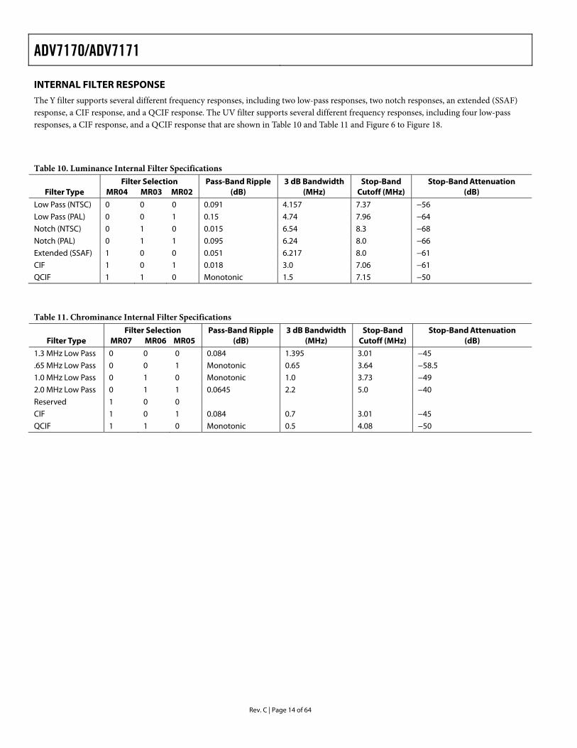
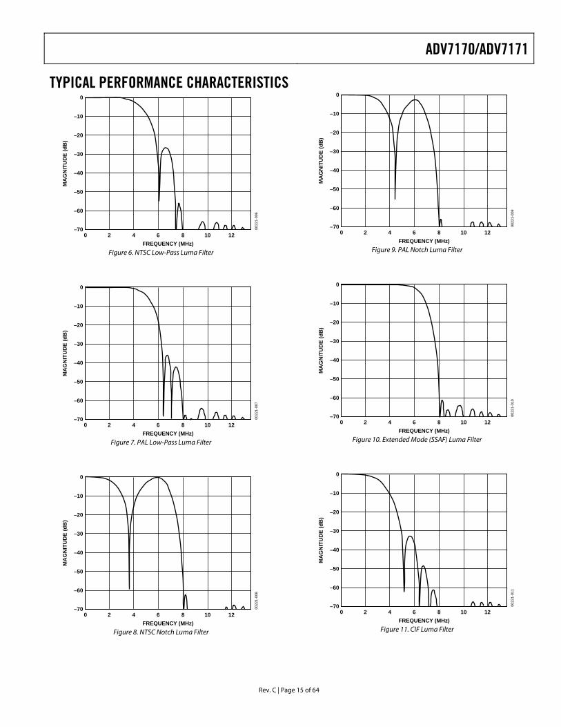
INTERNAL FILTER RESPONSE The Y filter supports several different frequency responses, including two low-pass responses, two notch responses, an extended (SSAF) response, a CIF response, and a QCIF response. The UV filter supports several different frequency responses, including four low-pass responses, a CIF response, and a QCIF response that are shown in Table 10 and Table 11 and Figure 6 to Figure 18.
Table 10. Luminance Internal Filter Specifications
Filter Type Filter Selection
MR04 MR03 MR02 Pass-Band Ripple
(dB) 3 dB Bandwidth
(MHz) Stop-Band
Cutoff (MHz) Stop-Band Attenuation
(dB) Low Pass (NTSC) 0 0 0 0.091 4.157 7.37 −56 Low Pass (PAL) 0 0 1 0.15 4.74 7.96 −64 Notch (NTSC) 0 1 0 0.015 6.54 8.3 −68 Notch (PAL) 0 1 1 0.095 6.24 8.0 −66 Extended (SSAF) 1 0 0 0.051 6.217 8.0 −61 CIF 1 0 1 0.018 3.0 7.06 −61 QCIF 1 1 0 Monotonic 1.5 7.15 −50
Table 11. Chrominance Internal Filter Specifications
Filter Type Filter Selection
MR07 MR06 MR05 Pass-Band Ripple
(dB) 3 dB Bandwidth
(MHz) Stop-Band
Cutoff (MHz) Stop-Band Attenuation
(dB) 1.3 MHz Low Pass 0 0 0 0.084 1.395 3.01 −45 .65 MHz Low Pass 0 0 1 Monotonic 0.65 3.64 −58.5 1.0 MHz Low Pass 0 1 0 Monotonic 1.0 3.73 −49 2.0 MHz Low Pass 0 1 1 0.0645 2.2 5.0 −40 Reserved 1 0 0 CIF 1 0 1 0.084 0.7 3.01 −45 QCIF 1 1 0 Monotonic 0.5 4.08 −50
ADV7170/ADV7171
Rev. C | Page 15 of 64
TYPICAL PERFORMANCE CHARACTERISTICS 0
–700
0022
1-00
6
FREQUENCY (MHz)
MA
GN
ITU
DE
(dB
)
–10
–20
–30
–40
–50
–60
2 4 6 8 10 12
Figure 6. NTSC Low-Pass Luma Filter
0
–700
0022
1-00
7
FREQUENCY (MHz)
MA
GN
ITU
DE
(dB
)
–10
–20
–30
–40
–50
–60
2 4 6 8 10 12
Figure 7. PAL Low-Pass Luma Filter
0
–700
0022
1-00
8
FREQUENCY (MHz)
MA
GN
ITU
DE
(dB
)
–10
–20
–30
–40
–50
–60
2 4 6 8 10 12
Figure 8. NTSC Notch Luma Filter
0
–700
0022
1-00
9
FREQUENCY (MHz)
MA
GN
ITU
DE
(dB
)
–10
–20
–30
–40
–50
–60
2 4 6 8 10 12
Figure 9. PAL Notch Luma Filter
0
–700
0022
1-01
0
FREQUENCY (MHz)
MA
GN
ITU
DE
(dB
)
–10
–20
–30
–40
–50
–60
2 4 6 8 10 12
Figure 10. Extended Mode (SSAF) Luma Filter
0
–700
0022
1-01
1
FREQUENCY (MHz)
MA
GN
ITU
DE
(dB
)
–10
–20
–30
–40
–50
–60
2 4 6 8 10 12
Figure 11. CIF Luma Filter
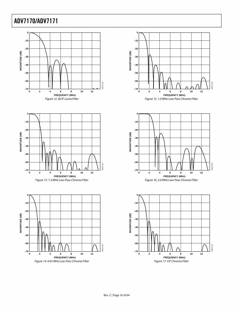
ADV7170/ADV7171
Rev. C | Page 16 of 64
0
–700
0022
1-01
2
FREQUENCY (MHz)
MA
GN
ITU
DE
(dB
)
–10
–20
–30
–40
–50
–60
2 4 6 8 10 12
Figure 12. QCIF Luma Filter
0
–700
0022
1-01
3
FREQUENCY (MHz)
MA
GN
ITU
DE
(dB
)
–10
–20
–30
–40
–50
–60
2 4 6 8 10 12
Figure 13. 1.3 MHz Low-Pass Chroma Filter
0
–700
0022
1-01
4
FREQUENCY (MHz)
MA
GN
ITU
DE
(dB
)
–10
–20
–30
–40
–50
–60
2 4 6 8 10 12
Figure 14. 0.65 MHz Low-Pass Chroma Filter
0
–700
0022
1-01
5
FREQUENCY (MHz)
MA
GN
ITU
DE
(dB
)
–10
–20
–30
–40
–50
–60
2 4 6 8 10 12
Figure 15. 1.0 MHz Low-Pass Chroma Filter
0
–700
0022
1-01
6
FREQUENCY (MHz)
MA
GN
ITU
DE
(dB
)
–10
–20
–30
–40
–50
–60
2 4 6 8 10 12
Figure 16. 2.0 MHz Low-Pass Chroma Filter
0
–700
0022
1-01
7
FREQUENCY (MHz)
MA
GN
ITU
DE
(dB
)
–10
–20
–30
–40
–50
–60
2 4 6 8 10 12
Figure 17. CIF Chroma Filter

ADV7170/ADV7171
Rev. C | Page 17 of 64
0
–700
0022
1-01
8
FREQUENCY (MHz)
MA
GN
ITU
DE
(dB
)
–10
–20
–30
–40
–50
–60
2 4 6 8 10 12
Figure 18. QCIF Chroma Filter
ADV7170/ADV7171
Rev. C | Page 18 of 64
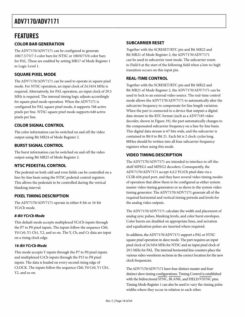
FEATURES COLOR BAR GENERATION The ADV7170/ADV7171 can be configured to generate 100/7.5/75/7.5 color bars for NTSC or 100/0/75/0 color bars for PAL. These are enabled by setting MR17 of Mode Register 1 to Logic Level 1.
SQUARE PIXEL MODE The ADV7170/ADV7171 can be used to operate in square pixel mode. For NTSC operation, an input clock of 24.5454 MHz is required. Alternatively, for PAL operation, an input clock of 29.5 MHz is required. The internal timing logic adjusts accordingly for square pixel mode operation. When the ADV7171 is configured for PAL square pixel mode, it supports 768 active pixels per line. NTSC square pixel mode supports 640 active pixels per line.
COLOR SIGNAL CONTROL The color information can be switched on and off the video output using Bit MR24 of Mode Register 2.
BURST SIGNAL CONTROL The burst information can be switched on and off the video output using Bit MR25 of Mode Register 2.
NTSC PEDESTAL CONTROL The pedestal on both odd and even fields can be controlled on a line-by-line basis using the NTSC pedestal control registers. This allows the pedestals to be controlled during the vertical blanking interval.
PIXEL TIMING DESCRIPTION The ADV7170/ADV7171 operate in either 8-bit or 16-bit YCrCb mode.
8-Bit YCrCb Mode
This default mode accepts multiplexed YCrCb inputs through the P7 to P0 pixel inputs. The inputs follow the sequence Cb0, Y0 Cr0, Y1 Cb1, Y2, and so on. The Y, Cb, and Cr data are input on a rising clock edge.
16-Bit YCrCb Mode
This mode accepts Y inputs through the P7 to P0 pixel inputs and multiplexed CrCb inputs through the P15 to P8 pixel inputs. The data is loaded on every second rising edge of CLOCK. The inputs follow the sequence Cb0, Y0 Cr0, Y1 Cb1, Y2, and so on.
SUBCARRIER RESET Together with the SCRESET/RTC pin and Bit MR22 and Bit MR21 of Mode Register 2, the ADV7170/ADV7171 can be used in subcarrier reset mode. The subcarrier resets to Field 0 at the start of the following field when a low-to-high transition occurs on this input pin.
REAL-TIME CONTROL Together with the SCRESET/RTC pin and Bit MR22 and Bit MR21 of Mode Register 2, the ADV7170/ADV7171 can be used to lock to an external video source. The real-time control mode allows the ADV7170/ADV7171 to automatically alter the subcarrier frequency to compensate for line length variation. When the part is connected to a device that outputs a digital data stream in the RTC format (such as a ADV7185 video decoder, shown in Figure 19), the part automatically changes to the compensated subcarrier frequency on a line-by-line basis. This digital data stream is 67 bits wide, and the subcarrier is contained in Bit 0 to Bit 21. Each bit is 2 clock cycles long. 00Hex should be written into all four subcarrier frequency registers when using this mode.
VIDEO TIMING DESCRIPTION The ADV7170/ADV7171 are intended to interface to off-the-shelf MPEG1 and MPEG2 decoders. Consequently, the ADV7170/ADV7171 accept 4:2:2 YCrCb pixel data via a CCIR-656 pixel port, and they have several video timing modes of operation that allow them to be configured as either system master video timing generators or as slaves to the system video timing generator. The ADV7170/ADV7171 generate all of the required horizontal and vertical timing periods and levels for the analog video outputs.
The ADV7170/ADV7171 calculate the width and placement of analog sync pulses, blanking levels, and color burst envelopes. Color bursts are disabled on appropriate lines, and serration and equalization pulses are inserted where required.
In addition, the ADV7170/ADV7171 support a PAL or NTSC square pixel operation in slave mode. The part requires an input pixel clock of 24.5454 MHz for NTSC and an input pixel clock of 29.5 MHz for PAL. The internal horizontal line counters place the various video waveform sections in the correct location for the new clock frequencies.
The ADV7170/ADV7171 have four distinct master and four distinct slave timing configurations. Timing Control is established with the bidirectional SYNC, BLANK, and FIELD/VSYNC pins. Timing Mode Register 1 can also be used to vary the timing pulse widths where they occur in relation to each other.
ADV7170/ADV7171
Rev. C | Page 19 of 64
HSYNC
FIELD/VSYNC
CLOCK
GREEN/LUMA/Y
RED/CHROMA/V
BLUE/COMPOSITE/U
COMPOSITE
ADV7170/ADV7171
P7–P0
SCRESET/RTC
H/LTRANSITIONCOUNT START
LOW128
RTC
TIME SLOT: 01 14 67 68NOT USED IN
ADV7170/ADV7171
19
VALIDSAMPLE
INVALIDSAMPLE
FSCPLL INCREMENT1
8/LLC
5 BITSRESERVED
SEQUENCEBIT2
RESETBIT3
RESERVED4 BITS
RESERVED
21013
14 BITSRESERVED
0
VIDEODECODER
(FOR EXAMPLE,ADV7185)
COMPOSITE VIDEO(FOR EXAMPLE,VCR OR CABLE)
NOTES:1FSCPLL INCREMENT IS 22 BITS LONG, VALUE LOADED INTO ADV7170/ADV7171 FSC DDS REGISTER ISFSCPLL INCREMENTS BITS 21:0 PLUS BITS 0:9 OF SUBCARRIER FREQUENCY REGISTERS. ALL ZEROS SHOULDBE WRITTEN TO THE SUBCARRIER FREQUENCY REGISTERS OF THE ADV7170/ADV7171.
2SEQUENCE BITPAL: 0 = LINE NORMAL, 1 = LINE INVERTEDNTSC: 0 = NO CHANGE
3RESET BITRESET ADV7170/ADV7171 DDS 00
221-
019
Figure 19. RTC Timing and Connections
Vertical Blanking Data Insertion
It is possible to allow encoding of incoming YCbCr data on those lines of VBI that do not bear line sync or pre-/post-equalization pulses (see Figure 21 to Figure 32). This mode of operation is called “partial blanking” and is selected by setting MR32 to 1. It allows the insertion of any VBI data (opened VBI) into the encoded output waveform. This data is present in the digitized incoming YcbCr data stream (for example, WSS data, CGMS, VPS, and so on). Alternatively, the entire VBI may be blanked (no VBI data inserted) on these lines by setting MR32 to 0.
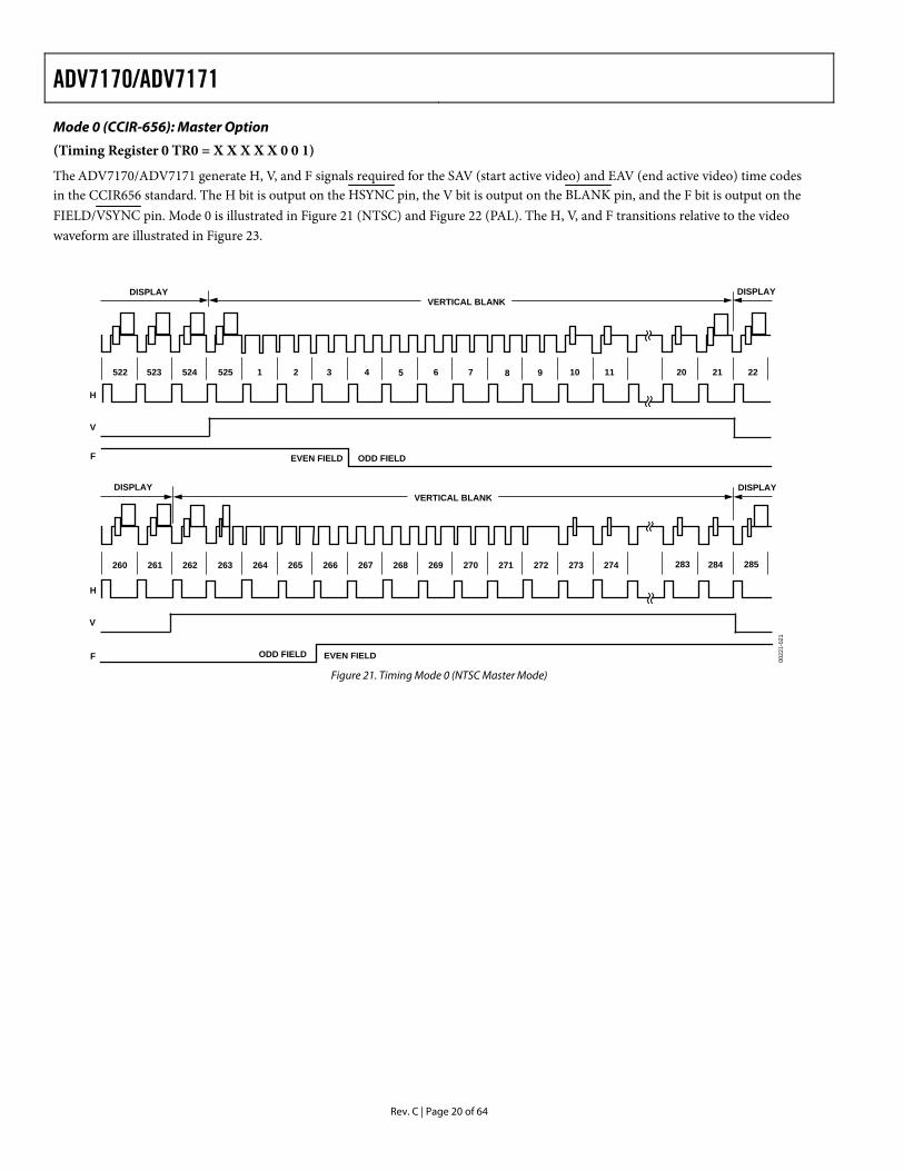
Mode 0 (CCIR-656): Slave Option
(Timing Register 0 TR0 = X X X X X 0 0 0)
The ADV7170/ADV7171 are controlled by the SAV (start active video) and EAV (end active video) time codes in the pixel data. All timing information is transmitted using a 4-byte synchroni-zation pattern. A synchronization pattern is sent immediately before and after each line during active picture and retrace. Mode 0 is shown in Figure 20. The HSYNC, FIELD/VSYNC, and BLANK (if not used) pins should be tied high during this mode.
Y Cr Y F
F00
00
XY
80
10
80
10
FF
00
FF
AB
AB
AB
80
10
80
10
FF
00
00
XY
Cb
Y Cr
CbY C
bYCr
EAV CODE SAV CODE
ANCILLARY DATA(HANC)
4 CLOCK 4 CLOCK 268 CLOCK 1440 CLOCK
4 CLOCK 4 CLOCK 280 CLOCK 1440 CLOCK
END OF ACTIVEVIDEO LINE
START OF ACTIVEVIDEO LINE
ANALOGVIDEO
INPUT PIXELS
NTSC/PAL M SYSTEM(525 LINES/60Hz)
PAL SYSTEM(625 LINES/50Hz)
Y
0022
1-02
0
Figure 20. Timing Mode 0 (Slave Mode)
ADV7170/ADV7171
Rev. C | Page 20 of 64
Mode 0 (CCIR-656): Master Option
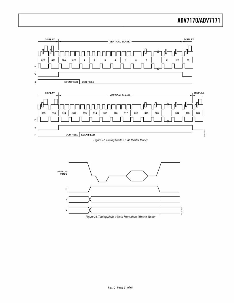
(Timing Register 0 TR0 = X X X X X 0 0 1)
The ADV7170/ADV7171 generate H, V, and F signals required for the SAV (start active video) and EAV (end active video) time codes in the CCIR656 standard. The H bit is output on the HSYNC pin, the V bit is output on the BLANK pin, and the F bit is output on the FIELD/VSYNC pin. Mode 0 is illustrated in (NTSC) and (PAL). The H, V, and F transitions relative to the video waveform are illustrated in .
Figure 21 Figure 22Figure 23
522 523 524 525 1 2 3 4 5 6 7 8 9 10 11 20 21 22
DISPLAY DISPLAYVERTICAL BLANK
ODD FIELDEVEN FIELD
H
V
F
260 261 262 263 264 265 266 267 268 269 270 271 272 273 274 283 284 285
ODD FIELD EVEN FIELD
DISPLAY DISPLAYVERTICAL BLANK
H
V
F 0022
1-02
1
Figure 21. Timing Mode 0 (NTSC Master Mode)
ADV7170/ADV7171
Rev. C | Page 21 of 64
622 623 624 625 1 2 3 4 5 6 7 21 22 23
DISPLAY DISPLAYVERTICAL BLANK
H
V
F ODD FIELDEVEN FIELD
309 310 311 312 314 315 316 317 318 319 320 334 335 336
DISPLAY DISPLAYVERTICAL BLANK
H
V
F ODD FIELD EVEN FIELD
313
0022
1-02
2
Figure 22. Timing Mode 0 (PAL Master Mode)
ANALOGVIDEO
H
F
V
0022
1-02
3
Figure 23. Timing Mode 0 Data Transitions (Master Mode)
ADV7170/ADV7171
Rev. C | Page 22 of 64
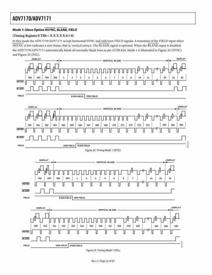
Mode 1: Slave Option HSYNC, BLANK, FIELD
(Timing Register 0 TR0 = X X X X X 0 1 0) In this mode the ADV7170/ADV7171 accept horizontal SYNC and odd/even FIELD signals. A transition of the FIELD input when HSYNC is low indicates a new frame, that is, vertical retrace. The BLANK signal is optional. When the BLANK input is disabled, the ADV7170/ADV7171 automatically blank all normally blank lines as per CCIR-624. Mode 1 is illustrated in (NTSC) and (PAL).
Figure 24Figure 25
260 261 262 263 264 265 266 267 268 269 270 271 272 273 274 283 284 285
ODD FIELD EVEN FIELD
DISPLAY DISPLAY
HSYNC
BLANK
FIELD
522 523 524 525 1 2 3 4 5 6 7 8 9 10 11 20 21 22
DISPLAY DISPLAY
ODD FIELDEVEN FIELD
BLANK
FIELD
VERTICAL BLANK
VERTICAL BLANK
HSYNC
0022
1-02
4
Figure 24. Timing Mode 1 (NTSC)
622 623 624 625 1 2 3 4 5 6 7 21 22 23
DISPLAY
ODD FIELDEVEN FIELD
HSYNC
BLANK
FIELD
DISPLAY
309 310 311 312 313 314 315 316 317 318 319 334 335 336
DISPLAY
ODD FIELD EVEN FIELD
HSYNC
BLANK
FIELD
DISPLAY
320
VERTICAL BLANK
VERTICAL BLANK
0022
1-02
5
Figure 25. Timing Mode 1 (PAL)
ADV7170/ADV7171
Rev. C | Page 23 of 64
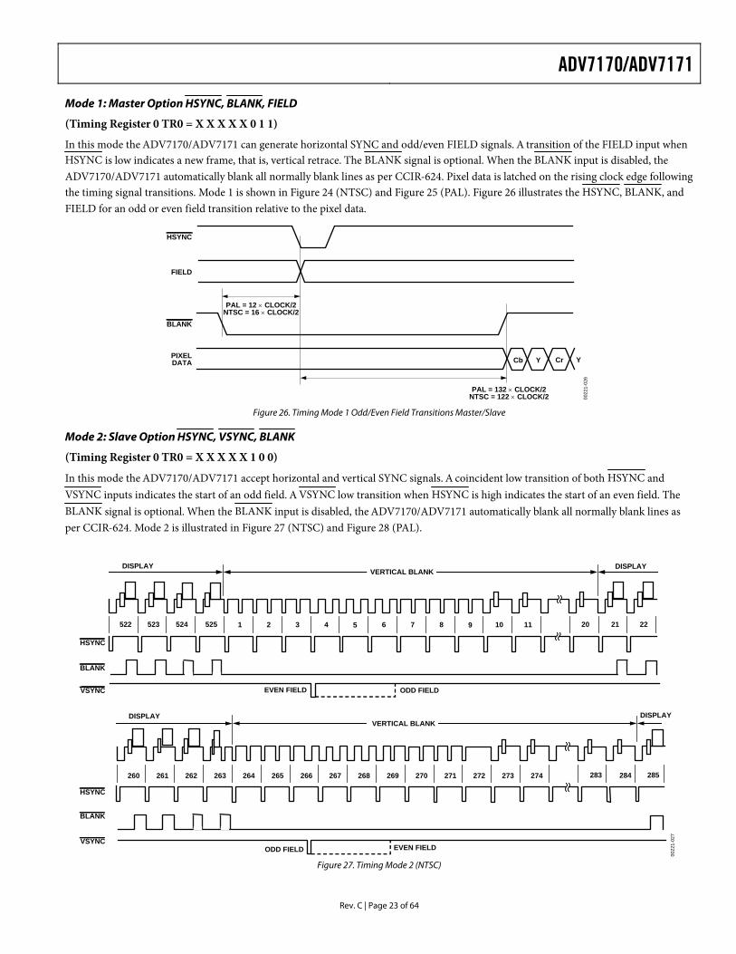
Mode 1: Master Option HSYNC, BLANK, FIELD
(Timing Register 0 TR0 = X X X X X 0 1 1)
In this mode the ADV7170/ADV7171 can generate horizontal SYNC and odd/even FIELD signals. A transition of the FIELD input when HSYNC is low indicates a new frame, that is, vertical retrace. The BLANK signal is optional. When the BLANK input is disabled, the ADV7170/ADV7171 automatically blank all normally blank lines as per CCIR-624. Pixel data is latched on the rising clock edge following the timing signal transitions. Mode 1 is shown in (NTSC) and (PAL). illustrates the Figure 24 Figure 25 Figure 26 HSYNC, BLANK, and FIELD for an odd or even field transition relative to the pixel data.
FIELD
PIXELDATA
PAL = 12 × CLOCK/2NTSC = 16 × CLOCK/2
PAL = 132 × CLOCK/2NTSC = 122 × CLOCK/2
Cb Y Cr Y
HSYNC
BLANK
0022
1-02
6
Figure 26. Timing Mode 1 Odd/Even Field Transitions Master/Slave
Mode 2: Slave Option HSYNC, VSYNC, BLANK
(Timing Register 0 TR0 = X X X X X 1 0 0)
In this mode the ADV7170/ADV7171 accept horizontal and vertical SYNC signals. A coincident low transition of both HSYNC and VSYNC inputs indicates the start of an odd field. A VSYNC low transition when HSYNC is high indicates the start of an even field. The BLANK signal is optional. When the BLANK input is disabled, the ADV7170/ADV7171 automatically blank all normally blank lines as per CCIR-624. Mode 2 is illustrated in (NTSC) and (PAL). Figure 27 Figure 28
522 523 524 525 1 2 3 4 5 6 7 8 9 10 11 20 21 22
DISPLAY DISPLAY
ODD FIELDEVEN FIELD
HSYNC
BLANK
VSYNC
260 261 262 263 264 265 266 267 268 269 270 271 272 273 274 283 284 285
ODD FIELD EVEN FIELD
DISPLAY DISPLAY
HSYNC
BLANK
VSYNC
VERTICAL BLANK
0022
1-02
7
VERTICAL BLANK
Figure 27. Timing Mode 2 (NTSC)
ADV7170/ADV7171
Rev. C | Page 24 of 64
622 623 624 625 1 2 3 4 5 6 7 21 22 23
DISPLAY
ODD FIELDEVEN FIELD
HSYNC
BLANK
VSYNC
DISPLAY
309 310 311 312 313 314 315 316 317 318 319 334 335 336
DISPLAY
ODD FIELD EVEN FIELD
HSYNC
BLANK
DISPLAY
320
VSYNC
VERTICAL BLANK
VERTICAL BLANK
0022
1-02
8
Figure 28. Timing Mode 2 (PAL)
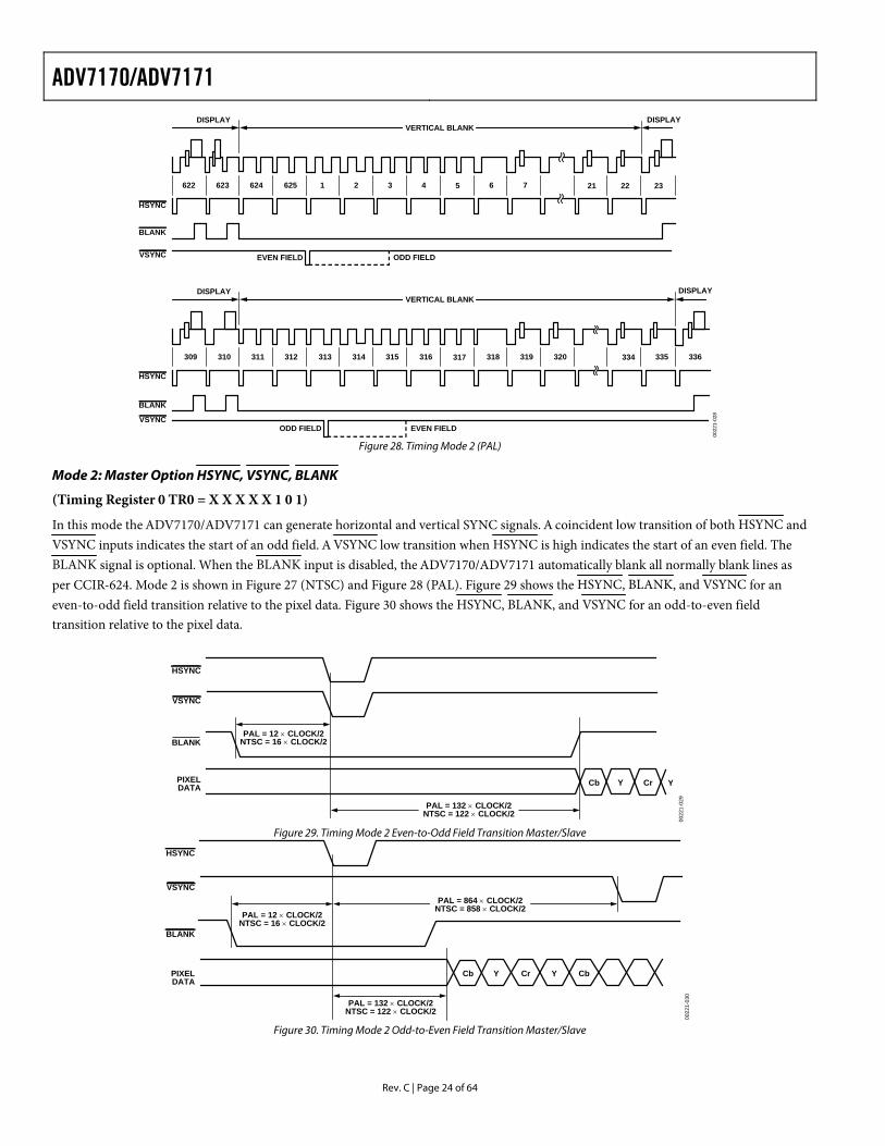
Mode 2: Master Option HSYNC, VSYNC, BLANK (Timing Register 0 TR0 = X X X X X 1 0 1)
In this mode the ADV7170/ADV7171 can generate horizontal and vertical SYNC signals. A coincident low transition of both HSYNC and VSYNC inputs indicates the start of an odd field. A VSYNC low transition when HSYNC is high indicates the start of an even field. The BLANK signal is optional. When the BLANK input is disabled, the ADV7170/ADV7171 automatically blank all normally blank lines as per CCIR-624. Mode 2 is shown in (NTSC) and (PAL). shows the Figure 27 Figure 28 Figure 29 HSYNC, BLANK, and VSYNC for an even-to-odd field transition relative to the pixel data. shows the Figure 30 HSYNC, BLANK, and VSYNC for an odd-to-even field transition relative to the pixel data.
PAL = 12 × CLOCK/2NTSC = 16 × CLOCK/2
HSYNC
VSYNC
PIXELDATA
PAL = 132 × CLOCK/2NTSC = 122 × CLOCK/2
Cb Y Cr Y
BLANK
0022
1-02
9
Figure 29. Timing Mode 2 Even-to-Odd Field Transition Master/Slave
PAL = 864 × CLOCK/2NTSC = 858 × CLOCK/2
PAL = 132 × CLOCK/2NTSC = 122 × CLOCK/2
HSYNC
VSYNC
PIXELDATA
PAL = 12 × CLOCK/2NTSC = 16 × CLOCK/2
Cb Y Cr Y Cb
BLANK
0022
1-03
0
Figure 30. Timing Mode 2 Odd-to-Even Field Transition Master/Slave
ADV7170/ADV7171
Rev. C | Page 25 of 64
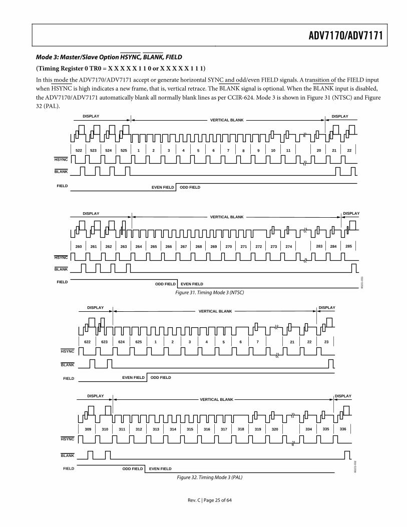
Mode 3: Master/Slave Option HSYNC, BLANK, FIELD
(Timing Register 0 TR0 = X X X X X 1 1 0 or X X X X X 1 1 1)
In this mode the ADV7170/ADV7171 accept or generate horizontal SYNC and odd/even FIELD signals. A transition of the FIELD input when HSYNC is high indicates a new frame, that is, vertical retrace. The BLANK signal is optional. When the BLANK input is disabled, the ADV7170/ADV7171 automatically blank all normally blank lines as per CCIR-624. Mode 3 is shown in (NTSC) and
(PAL). Figure 31 Figure
32
522 523 524 525 1 2 3 4 5 6 7 8 9 10 11 20 21 22
DISPLAY DISPLAYVERTICAL BLANK
ODD FIELDEVEN FIELD
BLANK
FIELD
260 261 262 263 264 265 266 267 268 269 270 271 272 273 274 283 284 285
DISPLAY DISPLAYVERTICAL BLANK
HSYNC
ODD FIELD
BLANK
FIELD
HSYNC
EVEN FIELD
0022
1-03
1
Figure 31. Timing Mode 3 (NTSC)
622 623 624 625 1 2 3 4 5 6 7 21 22 23
DISPLAY DISPLAYVERTICAL BLANK
ODD FIELDEVEN FIELD
BLANK
FIELD
309 310 311 312 314 315 316 317 318 319 320 334 335 336
DISPLAY DISPLAYVERTICAL BLANK
ODD FIELD EVEN FIELD
313
HSYNC
FIELD
HSYNC
BLANK
0022
1-03
2
Figure 32. Timing Mode 3 (PAL)
ADV7170/ADV7171
Rev. C | Page 26 of 64
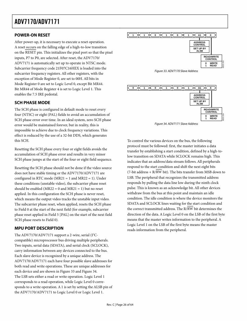
POWER-ON RESET After power-up, it is necessary to execute a reset operation. A reset occurs on the falling edge of a high-to-low transition on the RESET pin. This initializes the pixel port so that the pixel inputs, P7 to P0, are selected. After reset, the ADV7170/ ADV7171 is automatically set up to operate in NTSC mode. Subcarrier frequency code 21F07C16HEX is loaded into the subcarrier frequency registers. All other registers, with the exception of Mode Register 0, are set to 00H. All bits in Mode Register 0 are set to Logic Level 0, except Bit MR44. Bit MR44 of Mode Register 4 is set to Logic Level 1. This enables the 7.5 IRE pedestal.
SCH PHASE MODE The SCH phase is configured in default mode to reset every four (NTSC) or eight (PAL) fields to avoid an accumulation of SCH phase error over time. In an ideal system, zero SCH phase error would be maintained forever, but in reality, this is impossible to achieve due to clock frequency variations. This effect is reduced by the use of a 32-bit DDS, which generates this SCH.
Resetting the SCH phase every four or eight fields avoids the accumulation of SCH phase error and results in very minor SCH phase jumps at the start of the four or eight field sequence.
Resetting the SCH phase should not be done if the video source does not have stable timing or the ADV7170/ADV7171 are configured in RTC mode (MR21 = 1 and MR22 = 1). Under these conditions (unstable video), the subcarrier phase reset should be enabled (MR22 = 0 and MR21 = 1) but no reset applied. In this configuration the SCH phase is never reset, which means the output video tracks the unstable input video. The subcarrier phase reset, when applied, resets the SCH phase to Field 0 at the start of the next field (for example, subcarrier phase reset applied in Field 5 [PAL] on the start of the next field SCH phase resets to Field 0).
MPU PORT DESCRIPTION The ADV7170/ADV7171 support a 2-wire, serial (I2C-compatible) microprocessor bus driving multiple peripherals. Two inputs, serial data (SDATA), and serial clock (SCLOCK), carry information between any devices connected to the bus. Each slave device is recognized by a unique address. The ADV7170/ADV7171 each have four possible slave addresses for both read and write operations. These are unique addresses for each device and are shown in Figure 33 and Figure 34. The LSB sets either a read or write operation. Logic Level 1 corresponds to a read operation, while Logic Level 0 corre-sponds to a write operation. A 1 is set by setting the ALSB pin of the ADV7170/ADV7171 to Logic Level 0 or Logic Level 1.
1 X1 0 1 0 1 A1
ADDRESSCONTROLSET UP BY
ALSB
READ/WRITECONTROL0 WRITE1 READ
0022
1-03
3
Figure 33. ADV7170 Slave Address
0 X1 0 1 0 1 A1
ADDRESSCONTROLSET UP BY
ALSB
READ/WRITECONTROL0 WRITE1 READ
0022
1-03
4
Figure 34. ADV7171 Slave Address
To control the various devices on the bus, the following protocol must be followed: first, the master initiates a data transfer by establishing a start condition, defined by a high-to-low transition on SDATA while SCLOCK remains high. This indicates that an address/data stream follows. All peripherals respond to the start condition and shift the next eight bits (7-bit address + R/RW bit). The bits transfer from MSB down to LSB. The peripheral that recognizes the transmitted address responds by pulling the data line low during the ninth clock pulse. This is known as an acknowledge bit. All other devices withdraw from the bus at this point and maintain an idle condition. The idle condition is where the device monitors the SDATA and SCLOCK lines waiting for the start condition and the correct transmitted address. The R/RW bit determines the direction of the data. A Logic Level 0 on the LSB of the first byte means that the master writes information to the peripheral. A Logic Level 1 on the LSB of the first byte means the master reads information from the peripheral.

ADV7170/ADV7171
Rev. C | Page 27 of 64
The ADV7170/ADV7171 act as standard slave devices on the bus. The data on the SDATA pin is eight bits long, supporting the 7-bit addresses plus the R/RW bit. The ADV7170 has 48 subaddresses, and the ADV7171 has 26 subaddresses to enable access to the internal registers. It therefore interprets the first byte as the device address and the second byte as the starting subaddress. The subaddresses’ auto-increment allows data to be written to or read from the starting subaddress. A data transfer is always terminated by a stop condition. The user can also access any unique subaddress register on a one-by-one basis without having to update all the registers. There is one exception. The subcarrier frequency registers should be updated in sequence, starting with Subcarrier Frequency Register 0. The auto-increment function should then be used to increment and access Subcarrier Frequency Register 1, Subcarrier Frequency Register 2, and Subcarrier Frequency Register 3. The subcarrier frequency registers should not be accessed independently.
Stop and start conditions can be detected at any stage during the data transfer. If these conditions are asserted out of sequence with normal read and write operations, they cause an immediate jump to the idle condition. During a given SCLOCK high period, the user should issue only one start condition, one stop condition, or a single stop condition followed by a single start condition. If an invalid subaddress is issued by the user, the ADV7170/ADV7171 do not issue an acknowledge, and they return to the idle condition. If in auto-increment mode the user exceeds the highest subaddress, the following action is taken:
In read mode, the highest subaddress register contents continue to be output until the master device issues a no-acknowledge. This indicates the end of a read. A no-acknowledge condition is where the SDATA line is not pulled low on the ninth pulse.
In write mode, the data for the invalid byte is not loaded into any subaddress register, a no-acknowledge is issued by the ADV7170/ADV7171, and the part returns to the idle condition.
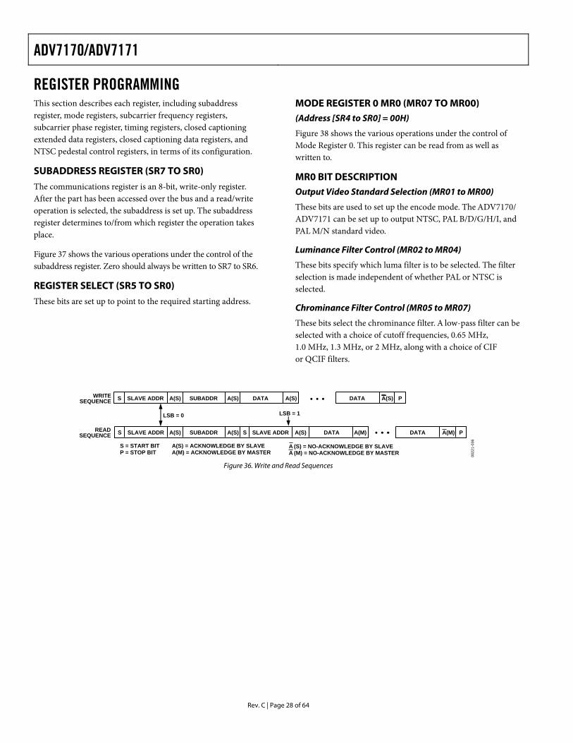
Figure 35 illustrates an example of data transfer for a read sequence and the start and stop conditions.
Figure 36 shows bus write and read sequences.
SDATA
SCLOCK
START ADDR R/W ACK SUBADDRESS ACK DATA ACK STOP1–7 8 9S 1–7 1–7 P
0022
1-03
5
8 9 8 9
Figure 35. Bus Data Transfer
REGISTER ACCESSES The MPU can write to or read from all of the ADV7170/ ADV7171 registers except the subaddress register, which is a write-only register. The subaddress register determines which register the next read or write operation accesses. All commu-nications with the part through the bus start with an access to the subaddress register. A read/write operation is performed from/to the target address, which then increments to the next address until a stop command on the bus is performed.
ADV7170/ADV7171
Rev. C | Page 28 of 64
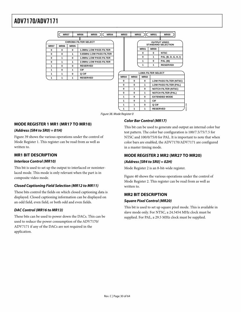
REGISTER PROGRAMMING MODE REGISTER 0 MR0 (MR07 TO MR00) This section describes each register, including subaddress
register, mode registers, subcarrier frequency registers, subcarrier phase register, timing registers, closed captioning extended data registers, closed captioning data registers, and NTSC pedestal control registers, in terms of its configuration.
(Address [SR4 to SR0] = 00H)
Figure 38 shows the various operations under the control of Mode Register 0. This register can be read from as well as written to.
SUBADDRESS REGISTER (SR7 TO SR0) MR0 BIT DESCRIPTION The communications register is an 8-bit, write-only register. After the part has been accessed over the bus and a read/write operation is selected, the subaddress is set up. The subaddress register determines to/from which register the operation takes place.
Output Video Standard Selection (MR01 to MR00)
These bits are used to set up the encode mode. The ADV7170/ ADV7171 can be set up to output NTSC, PAL B/D/G/H/I, and PAL M/N standard video.
Luminance Filter Control (MR02 to MR04) Figure 37 shows the various operations under the control of the subaddress register. Zero should always be written to SR7 to SR6. These bits specify which luma filter is to be selected. The filter
selection is made independent of whether PAL or NTSC is selected. REGISTER SELECT (SR5 TO SR0)
These bits are set up to point to the required starting address. Chrominance Filter Control (MR05 to MR07)
These bits select the chrominance filter. A low-pass filter can be selected with a choice of cutoff frequencies, 0.65 MHz, 1.0 MHz, 1.3 MHz, or 2 MHz, along with a choice of CIF or QCIF filters.
WRITESEQUENCE
READSEQUENCE
S SLAVE ADDR A(S) SUBADDR A(S) DATA DATA A(S) P
S SLAVE ADDR A(S) SUBADDR A(S) S SLAVE ADDR A(S) DATA DATAA(M) A(M) P
S = START BITP = STOP BIT
A(S) = ACKNOWLEDGE BY SLAVEA(M) = ACKNOWLEDGE BY MASTER
A (S) = NO-ACKNOWLEDGE BY SLAVEA (M) = NO-ACKNOWLEDGE BY MASTER
LSB = 0 LSB = 1
0022
1-03
6
A(S)
Figure 36. Write and Read Sequences
ADV7170/ADV7171
Rev. C | Page 29 of 64
ADV7171 SUBADDRESS REGISTER
SR5 SR4 SR3 SR2 SR1 SR0
0 0 0 0 0 0 MODE REGISTER 0
0 0 0 0 0 1 MODE REGISTER 1
0 0 0 0 1 0 MODE REGISTER 2
0 0 0 0 1 1 MODE REGISTER 3
0 0 0 1 0 0 MODE REGISTER 4
0 0 0 1 0 1 RESERVED
0 0 0 1 1 0 RESERVED
0 0 0 1 1 1 TIMING MODE REGISTER 0
0 0 1 0 0 0 TIMING MODE REGISTER 1
0 0 1 0 0 1 SUBCARRIER FREQUENCY REGISTER 0
0 0 1 0 1 0 SUBCARRIER FREQUENCY REGISTER 1
0 0 1 0 1 1 SUBCARRIER FREQUENCY REGISTER 2
0 0 1 1 0 0 SUBCARRIER FREQUENCY REGISTER 3
0 0 1 1 0 1 SUBCARRIER PHASE REGISTER
0 0 1 1 1 0 CLOSED CAPTIONING EXTENDED DATA BYTE 0
0 0 1 1 1 1 CLOSED CAPTIONING EXTENDED DATA BYTE 1
0 1 0 0 0 0 CLOSED CAPTIONING DATA BYTE 0
0 1 0 0 0 1 CLOSED CAPTIONING DATA BYTE 1
0 1 0 0 1 0 NTSC PEDESTAL CONTROL REG 0/PAL TTX CONTROL REG 0
0 1 0 0 1 1 NTSC PEDESTAL CONTROL REG 1/PAL TTX CONTROL REG 1
0 1 0 1 0 0 NTSC PEDESTAL CONTROL REG 2/PAL TTX CONTROL REG 2
0 1 0 1 0 1 NTSC PEDESTAL CONTROL REG 3/PAL TTX CONTROL REG 3
0 1 0 1 1 0 CGMS_WSS_0
0 1 0 1 1 1 CGMS_WSS_1
0 1 1 0 0 0 CGMS_WSS_2
0 1 1 0 0 1 TELETEXT REQUEST CONTROL REGISTER
ADV7170 SUBADDRESS REGISTER
SR5 SR4 SR3 SR2 SR1 SR0POWER-UP/
RESET VALUE(HEX)
POWER-UP/RESET VALUE
(HEX)0 0 0 0 0 0 0000
5858
0000
0000
1010
0000
0000
0000
0000
16*16*
7C7C
F0
21
00
00
00
00
00
00
00
00
00
00
00
00
00
F0
21
00
00
00
00
00
00
00
00
00
00
00
00
00
00
00
00
00
00
00
00
00
00
00
00
00
00
00
00
00
00
00
00
00
00
00
MODE REGISTER 0
0 0 0 0 0 1 MODE REGISTER 1
0 0 0 0 1 0 MODE REGISTER 2
0 0 0 0 1 1 MODE REGISTER 3
0 0 0 1 0 0 MODE REGISTER 4
0 0 0 1 0 1 RESERVED
0 0 0 1 1 0 RESERVED
0 0 0 1 1 1 TIMING MODE REGISTER 0
0 0 1 0 0 0 TIMING MODE REGISTER 1
0 0 1 0 0 1 SUBCARRIER FREQUENCY REGISTER 0
0 0 1 0 1 0 SUBCARRIER FREQUENCY REGISTER 1
0 0 1 0 1 1 SUBCARRIER FREQUENCY REGISTER 2
0 0 1 1 0 0 SUBCARRIER FREQUENCY REGISTER 3
0 0 1 1 0 1 SUBCARRIER PHASE REGISTER
0 0 1 1 1 0 CLOSED CAPTIONING EXTENDED DATA BYTE 0
0 0 1 1 1 1 CLOSED CAPTIONING EXTENDED DATA BYTE 1
0 1 0 0 0 0 CLOSED CAPTIONING DATA BYTE 0
0 1 0 0 0 1 CLOSED CAPTIONING DATA BYTE 1
0 1 0 0 1 0 NTSC PEDESTAL CONTROL REG 0/PAL TTX CONTROL REG 0
0 1 0 0 1 1 NTSC PEDESTAL CONTROL REG 1/PAL TTX CONTROL REG 1
0 1 0 1 0 0 NTSC PEDESTAL CONTROL REG 2/PAL TTX CONTROL REG 2
0 1 0 1 0 1 NTSC PEDESTAL CONTROL REG 3/PAL TTX CONTROL REG 3
0 1 0 1 1 0 CGMS_WSS_0
0 1 0 1 1 1 CGMS_WSS_1
0 1 1 0 0 0 CGMS_WSS_2
0 1 1 0 0 1 TELETEXT REQUEST CONTROL REGISTER
0 1 1 0 1 0 RESERVED
0 1 1 0 1 1 RESERVED
0 1 1 1 0 0 RESERVED
0 1 1 1 0 1 RESERVED
0 1 1 1 1 0 MACROVISION REGISTERS
0 1 1 1 1 1 MACROVISION REGISTERS
1 0 0 0 0 0 MACROVISION REGISTERS
1 0 0 0 0 1 MACROVISION REGISTERS
1 0 0 0 1 0 MACROVISION REGISTERS
1 0 0 0 1 1 MACROVISION REGISTERS
1 0 0 1 0 0 MACROVISION REGISTERS
1 0 0 1 0 1 MACROVISION REGISTERS
1 0 0 1 1 0 MACROVISION REGISTERS
1 0 0 1 1 1 MACROVISION REGISTERS
1 0 1 0 0 0 MACROVISION REGISTERS
1 0 1 0 0 1 MACROVISION REGISTERS
1 0 1 0 1 0 MACROVISION REGISTERS
1 0 1 0 1 1 MACROVISION REGISTERS
1 0 1 1 0 0 MACROVISION REGISTERS
1 0 1 1 0 1 MACROVISION REGISTERS
1 0 1 1 1 0 MACROVISION REGISTERS
1 0 1 1 1 1 MACROVISION REGISTERS
SR4 SR3 SR2 SR1 SR0SR7 SR6 SR5
ZERO SHOULD BE WRITTENTO THESE BITS
SR7–SR5 (000)
0022
1-03
7
*SUBCARRIER FREQUENCY REGISTER 0 = 16 IS INCORRECT ON POWER-UP FOR NTSC. THIS REGISTER SHOULD BE PROGRAMMED TO 1F FOR ACCURATE FSC.
Figure 37. Subaddress Register Map
ADV7170/ADV7171
Rev. C | Page 30 of 64
MR01 MR00MR07 MR02MR03MR05MR06 MR04
MR07 MR06 MR050 0 00 0 10 1 00 1 11 0 01 0 11 1 01 1 1
1.3MHz LOW PASS FILTER0.65MHz LOW PASS FILTER1.0MHz LOW PASS FILTER2.0MHz LOW PASS FILTERRESERVEDCIFQ CIFRESERVED
CHROMA FILTER SELECT
MR04 MR03 MR020 0 00 0 10 1 00 0 11 0 01 0 11 1 01 1 1
LOW PASS FILTER (NTSC)LOW PASS FILTER (PAL)NOTCH FILTER (NTSC)NOTCH FILTER (PAL)EXTENDED MODECIFQ CIFRESERVED
LUMA FILTER SELECT
MR01 MR000 00 11 01 1
NTSCPAL (B, D, G, H, I)PAL (M)RESERVED
OUTPUT VIDEOSTANDARD SELECTION
0022
1-03
8
Figure 38. Mode Register 0
Color Bar Control (MR17) MODE REGISTER 1 MR1 (MR17 TO MR10)
This bit can be used to generate and output an internal color bar test pattern. The color bar configuration is 100/7.5/75/7.5 for NTSC and 100/0/75/0 for PAL. It is important to note that when color bars are enabled, the ADV7170/ADV7171 are configured in a master timing mode.
(Address (SR4 to SR0) = 01H)
Figure 39 shows the various operations under the control of Mode Register 1. This register can be read from as well as written to.
MR1 BIT DESCRIPTION MODE REGISTER 2 MR2 (MR27 TO MR20) Interlace Control (MR10) (Address [SR4 to SR0] = 02H) This bit is used to set up the output to interlaced or noninter-laced mode. This mode is only relevant when the part is in composite video mode.
Mode Register 2 is an 8-bit-wide register.
Figure 40 shows the various operations under the control of Mode Register 2. This register can be read from as well as written to. Closed Captioning Field Selection (MR12 to MR11)
These bits control the fields on which closed captioning data is displayed. Closed captioning information can be displayed on an odd field, even field, or both odd and even fields.
MR2 BIT DESCRIPTION Square Pixel Control (MR20)
This bit is used to set up square pixel mode. This is available in slave mode only. For NTSC, a 24.5454 MHz clock must be supplied. For PAL, a 29.5 MHz clock must be supplied.
DAC Control (MR16 to MR13)
These bits can be used to power down the DACs. This can be used to reduce the power consumption of the ADV7170/ ADV7171 if any of the DACs are not required in the application.
ADV7170/ADV7171
Rev. C | Page 31 of 64
MR11 MR10MR17 MR12MR13MR15MR16 MR14
CLOSED CAPTIONINGFIELD SELECTION
0 0 NO DATA OUT0 1 ODD FIELD ONLY1 0 EVEN FIELD ONLY1 1 DATA OUT
(BOTH FIELDS)
MR12 MR11
DAC ACONTROL
0 NORMAL1 POWER-DOWN
MR16
DAC DCONTROL
MR14
DAC CCONTROL
MR13MR15
INTERLACECONTROL
0 INTERLACED1 NONINTERLACED
MR10
COLOR BARCONTROL
0 DISABLE1 ENABLE
MR17
0 NORMAL1 POWER-DOWN
0 NORMAL1 POWER-DOWN
0 NORMAL1 POWER-DOWN
DAC BCONTROL
0022
1-03
9
Figure 39. Mode Register 1
MR21MR27 MR22MR23MR26 MR25 MR24 MR20
CHROMINANCECONTROL
0 ENABLE COLOR1 DISABLE COLOR
MR24
GENLOCK CONTROL
x 0 DISABLE GENLOCK0 1 ENABLE SUBCARRIER
RESET PIN1 1 ENABLE RTC PIN
MR22 MR21LOW POWER MODE
0 DISABLE1 ENABLE
MR26
SQUARE PIXELCONTROL
0 DISABLE1 ENABLE
MR20
BURSTCONTROL
0 ENABLE BURST1 DISABLE BURST
MR25
MR27 ACTIVE VIDEO LINEDURATION
0 720 PIXELS1 710 PIXELS/702 PIXELS
MR23RESERVED
0022
1-04
0
Figure 40. Mode Register 2
MR31 MR30MR37 MR32MR34 MR33MR35MR36
MR30MR31
RESERVED
VBI_OPEN
0 DISABLE1 ENABLE
MR32
DAC OUTPUT
0 COMPOSITE1 GREEN/LUMA/Y
MR33 DAC ABLUE/COMP/UBLUE/COMP/U
DAC BRED/CHROMA/VRED/CHROMA/V
DAC CGREEN/LUMA/YCOMPOSITE
DAC D
CHROMA OUTPUTSELECT
0 DISABLE1 ENABLE
MR34
TELETEXTENABLE
0 DISABLE1 ENABLE
MR35
TTXRQ BITMODE CONTROL
0 NORMAL1 BIT REQUEST
MR36
INPUT DEFAULTCOLOR
0 DISABLE1 ENABLE
MR3700
221-
041
Figure 41. Mode Register 3
Genlock Control (MR22 to MR21)
These bits control the genlock feature of the ADV7170/ ADV7171. Setting MR21 to a Logic Level 1 configures the SCRESET/RTC pin as an input. Setting MR22 to Logic Level 0 configures the SCRESET/RTC pin as a subcarrier reset input. Therefore, the subcarrier resets to Field 0 following a low-to-high transition on the SCRESET/RTC pin. Setting MR22 to Logic Level 1 configures the SCRESET/RTC pin as a real-time control input.
Active Video Line Duration (MR23)
This bit switches between two active video line durations. A 0 selects CCIR REC601 (720 pixels PAL/NTSC), and
a 1 selects ITU-R.BT470 standard for active video duration (710 pixels NTSC; 702 pixels PAL).
Chrominance Control (MR24)
This bit enables the color information to be switched on and off the video output.
Burst Control (MR25) This bit enables the burst information to be switched on and off the video output.
Low Power Mode (MR26) This bit enables the lower power mode of the ADV7170/ ADV7171, reducing the DAC current by 45%.
ADV7170/ADV7171
Rev. C | Page 32 of 64
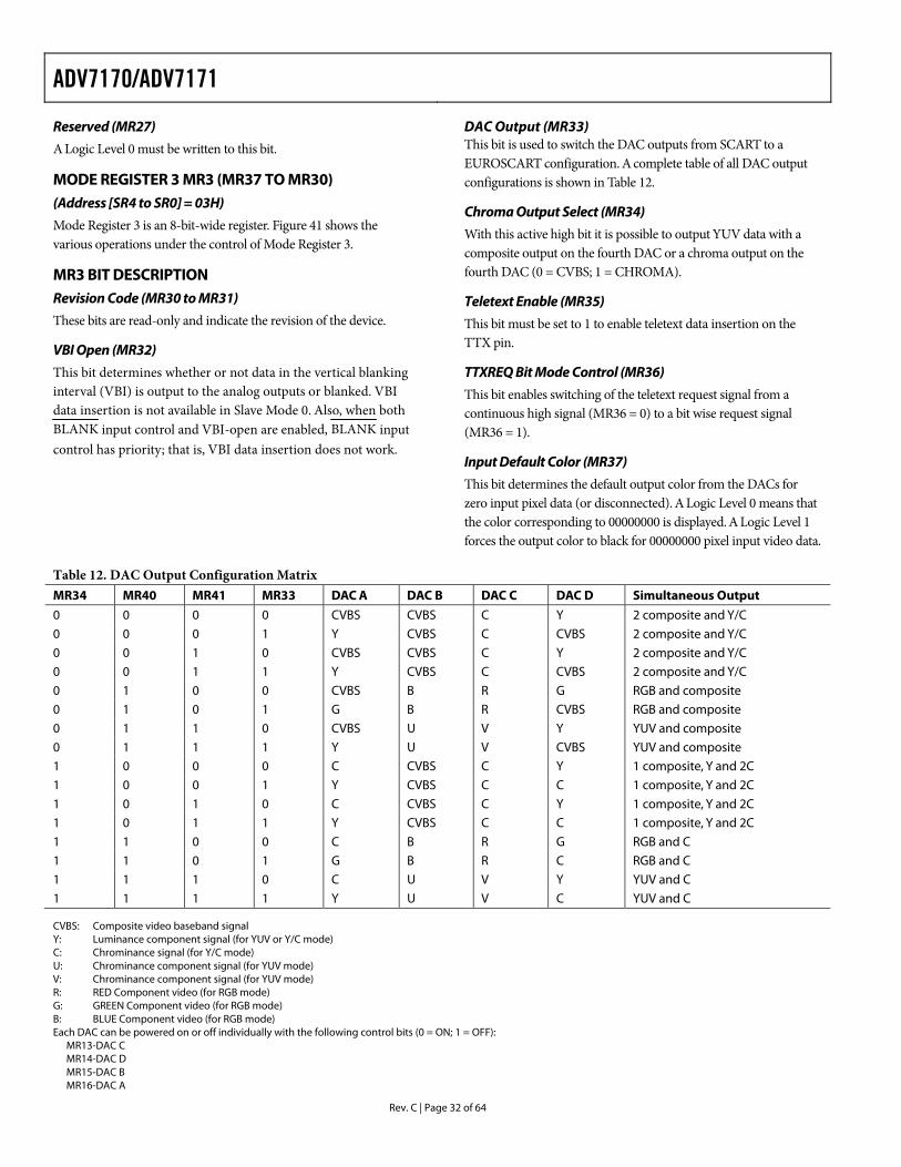
Reserved (MR27) A Logic Level 0 must be written to this bit.
MODE REGISTER 3 MR3 (MR37 TO MR30) (Address [SR4 to SR0] = 03H) Mode Register 3 is an 8-bit-wide register. Figure 41 shows the various operations under the control of Mode Register 3.
MR3 BIT DESCRIPTION Revision Code (MR30 to MR31) These bits are read-only and indicate the revision of the device.
VBI Open (MR32) This bit determines whether or not data in the vertical blanking interval (VBI) is output to the analog outputs or blanked. VBI data insertion is not available in Slave Mode 0. Also, when both BLANK input control and VBI-open are enabled, BLANK input control has priority; that is, VBI data insertion does not work.
DAC Output (MR33) This bit is used to switch the DAC outputs from SCART to a EUROSCART configuration. A complete table of all DAC output configurations is shown in Table 12.
Chroma Output Select (MR34) With this active high bit it is possible to output YUV data with a composite output on the fourth DAC or a chroma output on the fourth DAC (0 = CVBS; 1 = CHROMA).
Teletext Enable (MR35) This bit must be set to 1 to enable teletext data insertion on the TTX pin.
TTXREQ Bit Mode Control (MR36) This bit enables switching of the teletext request signal from a continuous high signal (MR36 = 0) to a bit wise request signal (MR36 = 1).
Input Default Color (MR37) This bit determines the default output color from the DACs for zero input pixel data (or disconnected). A Logic Level 0 means that the color corresponding to 00000000 is displayed. A Logic Level 1 forces the output color to black for 00000000 pixel input video data.
Table 12. DAC Output Configuration Matrix MR34 MR40 MR41 MR33 DAC A DAC B DAC C DAC D Simultaneous Output 0 0 0 0 CVBS CVBS C Y 2 composite and Y/C 0 0 0 1 Y CVBS C CVBS 2 composite and Y/C 0 0 1 0 CVBS CVBS C Y 2 composite and Y/C 0 0 1 1 Y CVBS C CVBS 2 composite and Y/C 0 1 0 0 CVBS B R G RGB and composite 0 1 0 1 G B R CVBS RGB and composite 0 1 1 0 CVBS U V Y YUV and composite 0 1 1 1 Y U V CVBS YUV and composite 1 0 0 0 C CVBS C Y 1 composite, Y and 2C 1 0 0 1 Y CVBS C C 1 composite, Y and 2C 1 0 1 0 C CVBS C Y 1 composite, Y and 2C 1 0 1 1 Y CVBS C C 1 composite, Y and 2C 1 1 0 0 C B R G RGB and C 1 1 0 1 G B R C RGB and C 1 1 1 0 C U V Y YUV and C 1 1 1 1 Y U V C YUV and C CVBS: Composite video baseband signal Y: Luminance component signal (for YUV or Y/C mode) C: Chrominance signal (for Y/C mode) U: Chrominance component signal (for YUV mode) V: Chrominance component signal (for YUV mode) R: RED Component video (for RGB mode) G: GREEN Component video (for RGB mode) B: BLUE Component video (for RGB mode) Each DAC can be powered on or off individually with the following control bits (0 = ON; 1 = OFF):
MR13-DAC C MR14-DAC D MR15-DAC B MR16-DAC A
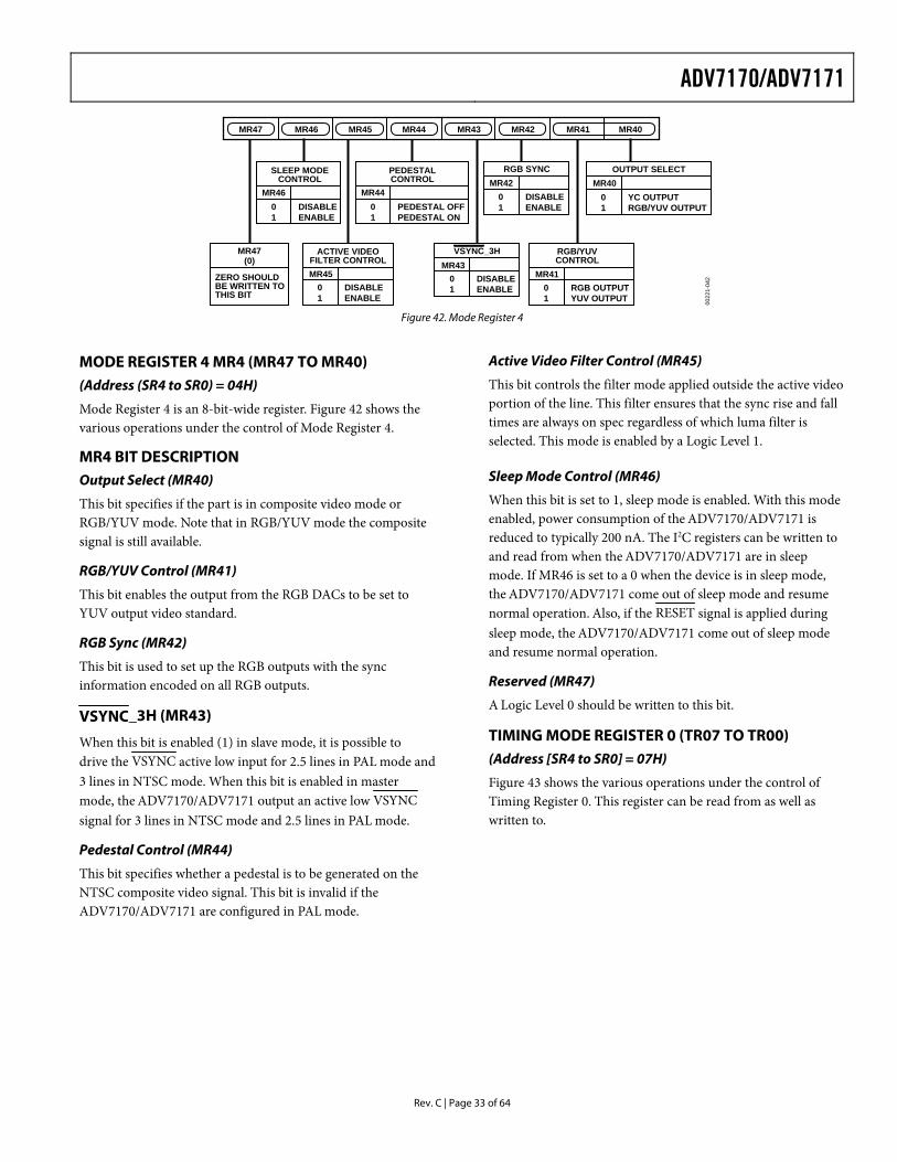
ADV7170/ADV7171
Rev. C | Page 33 of 64
MR41 MR40MR47 MR42MR44 MR43MR45MR46
OUTPUT SELECT
0 YC OUTPUT1 RGB/YUV OUTPUT
MR40RGB SYNC
0 DISABLE1 ENABLE
MR42PEDESTALCONTROL
0 PEDESTAL OFF1 PEDESTAL ON
MR44
SLEEP MODECONTROL
0 DISABLE1 ENABLE
MR46
ACTIVE VIDEOFILTER CONTROL
0 DISABLE1 ENABLE
MR45
MR47(0)
ZERO SHOULDBE WRITTEN TOTHIS BIT
VSYNC_3H
0 DISABLE1 ENABLE
MR43RGB/YUVCONTROL
0 RGB OUTPUT1 YUV OUTPUT
MR41
0022
1-04
2
Figure 42. Mode Register 4
MODE REGISTER 4 MR4 (MR47 TO MR40) (Address (SR4 to SR0) = 04H)
Mode Register 4 is an 8-bit-wide register. Figure 42 shows the various operations under the control of Mode Register 4.
MR4 BIT DESCRIPTION Output Select (MR40)
This bit specifies if the part is in composite video mode or RGB/YUV mode. Note that in RGB/YUV mode the composite signal is still available.
RGB/YUV Control (MR41)
This bit enables the output from the RGB DACs to be set to YUV output video standard.
RGB Sync (MR42)
This bit is used to set up the RGB outputs with the sync information encoded on all RGB outputs.
VSYNC_3H (MR43)
When this bit is enabled (1) in slave mode, it is possible to drive the VSYNC active low input for 2.5 lines in PAL mode and 3 lines in NTSC mode. When this bit is enabled in master mode, the ADV7170/ADV7171 output an active low VSYNC signal for 3 lines in NTSC mode and 2.5 lines in PAL mode.
Pedestal Control (MR44)
This bit specifies whether a pedestal is to be generated on the NTSC composite video signal. This bit is invalid if the ADV7170/ADV7171 are configured in PAL mode.
Active Video Filter Control (MR45)
This bit controls the filter mode applied outside the active video portion of the line. This filter ensures that the sync rise and fall times are always on spec regardless of which luma filter is selected. This mode is enabled by a Logic Level 1.
Sleep Mode Control (MR46)
When this bit is set to 1, sleep mode is enabled. With this mode enabled, power consumption of the ADV7170/ADV7171 is reduced to typically 200 nA. The I2C registers can be written to and read from when the ADV7170/ADV7171 are in sleep mode. If MR46 is set to a 0 when the device is in sleep mode, the ADV7170/ADV7171 come out of sleep mode and resume normal operation. Also, if the RESET signal is applied during sleep mode, the ADV7170/ADV7171 come out of sleep mode and resume normal operation.
Reserved (MR47)
A Logic Level 0 should be written to this bit.
TIMING MODE REGISTER 0 (TR07 TO TR00) (Address [SR4 to SR0] = 07H)
Figure 43 shows the various operations under the control of Timing Register 0. This register can be read from as well as written to.
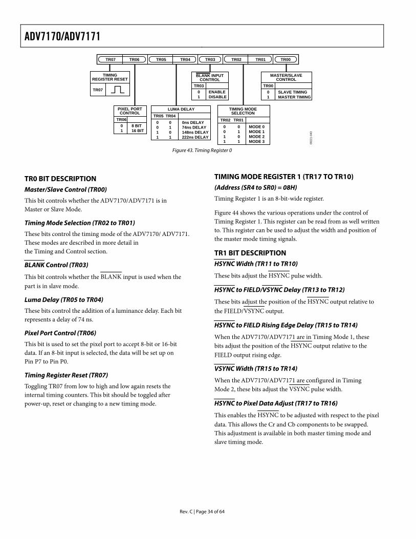
ADV7170/ADV7171
Rev. C | Page 34 of 64
TR01 TR00TR07 TR02TR03TR05TR06 TR04
TIMINGREGISTER RESET
TR07
BLANK INPUTCONTROL
0 ENABLE1 DISABLE
TR03
PIXEL PORTCONTROL
0 8 BIT1 16 BIT
TR06
MASTER/SLAVECONTROL
0 SLAVE TIMING1 MASTER TIMING
TR00
LUMA DELAY
0 0 0ns DELAY0 1 74ns DELAY1 0 148ns DELAY1 1 222ns DELAY
TR05 TR04TIMING MODESELECTION
0 0 MODE 00 1 MODE 11 0 MODE 21 1 MODE 3
TR02 TR01
0022
1-04
3
Figure 43. Timing Register 0
TR0 BIT DESCRIPTION Master/Slave Control (TR00)
This bit controls whether the ADV7170/ADV7171 is in Master or Slave Mode.
Timing Mode Selection (TR02 to TR01)
These bits control the timing mode of the ADV7170/ ADV7171. These modes are described in more detail in the Timing and Control section.
BLANK Control (TR03)
This bit controls whether the BLANK input is used when the part is in slave mode.
Luma Delay (TR05 to TR04)
These bits control the addition of a luminance delay. Each bit represents a delay of 74 ns.
Pixel Port Control (TR06)
This bit is used to set the pixel port to accept 8-bit or 16-bit data. If an 8-bit input is selected, the data will be set up on Pin P7 to Pin P0.
Timing Register Reset (TR07)
Toggling TR07 from low to high and low again resets the internal timing counters. This bit should be toggled after power-up, reset or changing to a new timing mode.
TIMING MODE REGISTER 1 (TR17 TO TR10) (Address (SR4 to SR0) = 08H)
Timing Register 1 is an 8-bit-wide register.
Figure 44 shows the various operations under the control of Timing Register 1. This register can be read from as well written to. This register can be used to adjust the width and position of the master mode timing signals.
TR1 BIT DESCRIPTION HSYNC Width (TR11 to TR10)
These bits adjust the HSYNC pulse width.
HSYNC to FIELD/VSYNC Delay (TR13 to TR12)
These bits adjust the position of the HSYNC output relative to the FIELD/VSYNC output.
HSYNC to FIELD Rising Edge Delay (TR15 to TR14)
When the ADV7170/ADV7171 are in Timing Mode 1, these bits adjust the position of the HSYNC output relative to the FIELD output rising edge.
VSYNC Width (TR15 to TR14)
When the ADV7170/ADV7171 are configured in Timing Mode 2, these bits adjust the VSYNC pulse width.
HSYNC to Pixel Data Adjust (TR17 to TR16)
This enables the HSYNC to be adjusted with respect to the pixel data. This allows the Cr and Cb components to be swapped. This adjustment is available in both master timing mode and slave timing mode.

ADV7170/ADV7171
Rev. C | Page 35 of 64
TR11 TR10TR17 TR12TR13TR15TR16 TR14
HSYNC TO PIXELDATA ADJUST
TR17 TR16
0 0 0 × TPCLK0 1 1 × TPCLK1 0 2 × TPCLK1 1 3 × TPCLK
HSYNC TOFIELD/VSYNC DELAY
TR13 TR120 0 0 × TPCLK0 1 4 × TPCLK1 0 8 × TPCLK1 1 16 × TPCLK
TB
HSYNC WIDTH
0 0 1 × TPCLK0 1 4 × TPCLK1 0 16 × TPCLK1 1 128 × TPCLK
TR11 TR10 TA
HSYNC TO FIELDRISING EDGE DELAY
(MODE 1 ONLY)
x 0 TBx 1 TB + 32μs
TR15 TR14 TC
VSYNC WIDTH(MODE 2 ONLY)
TR15 TR14
0 0 1 × TPCLK0 1 4 × TPCLK1 0 16 × TPCLK1 1 128 × TPCLK
LINE 313 LINE 314LINE 1
TB
TIMING MODE 1 (MASTER/PAL)
FIELD/VSYNC
TC
TAHSYNC
0022
1-04
4
Figure 44. Timing Register 1
SUBCARRIER FREQUENCY REGISTERS 0 TO 3 (FSC3 TO FSC0) (Address [SR4 to SR00] = 09H to 0CH) These 8-bit-wide registers are used to set up the subcarrier frequency. The value of these registers is calculated by using the following equation, rounded to the nearest integer:
32227.
.×
LineVideoOneinCyclesClockMHzofNoLineVideoofLineOneinValuesFrequencySubcarrierofNo
For example, in NTSC mode,
FhCFdalueVFrequencySubcarrier 1072156940854221716
5.227 32 ==×=
Note that on power-up, FSC Register 0 is set to 16h. A value of 1F as derived above is recommended.
Program as follows:
FSC Register 0: 1FH FSC Register 2: 7CH FSC Register 3: F0H FSC Register 4: 21H
Figure 45 shows how the frequency is set up by the four registers.
SUBCARRIERFREQUENCY
REG 3FSC30 FSC29 FSC27 FSC25FSC28 FSC24FSC31 FSC26
SUBCARRIERFREQUENCY
REG 2FSC22 FSC21 FSC19 FSC17FSC20 FSC16FSC23 FSC18
SUBCARRIERFREQUENCY
REG 1FSC14 FSC13 FSC11 FSC9FSC12 FSC8FSC15 FSC10
SUBCARRIERFREQUENCY
REG 0FSC6 FSC5 FSC3 FSC1FSC4 FSC0FSC7 FSC2
0022
1-04
5
Figure 45. Subcarrier Frequency Register
SUBCARRIER PHASE REGISTERS (FP7 TO FP0) (Address [SR4 to SR0] = 0DH)
This 8-bit-wide register is used to set up the subcarrier phase. Each bit represents 1.41°. For normal operation this register is set to 00Hex.
CLOSED CAPTIONING EVEN FIELD DATA REGISTER 1 TO 0 (CED15 TO CED0) (Address [SR4–SR0] = 0E to 0FH)
These 8-bit-wide registers are used to set up the closed captioning extended data bytes on even fields. Figure 46 shows how the high and low bytes are set up in the registers.
BYTE 1
BYTE 0 CED6 CED5 CED3 CED1CED4 CED2 CED0CED7
CED14 CED13 CED11 CED9CED12 CED10 CED8CED15
0022
1-04
6
Figure 46. Closed Captioning Extended Data Register
CLOSED CAPTIONING ODD FIELD DATA REGISTERS 1 TO 0 (CCD15 TO CCD0) (Subaddress [SR4 to SR0] = 10H to 11H)
These 8-bit-wide registers are used to set up the closed captioning data bytes on odd fields. Figure 47 shows how the high and low bytes are set up in the registers.
BYTE 1
BYTE 0 CCD6 CCD5 CCD3 CCD1CCD4 CCD2 CCD0CCD7
CCD14 CCD13 CCD11 CCD9CCD12 CCD10 CCD8CCD15
0022
1-04
7
Figure 47. Closed Captioning Data Register
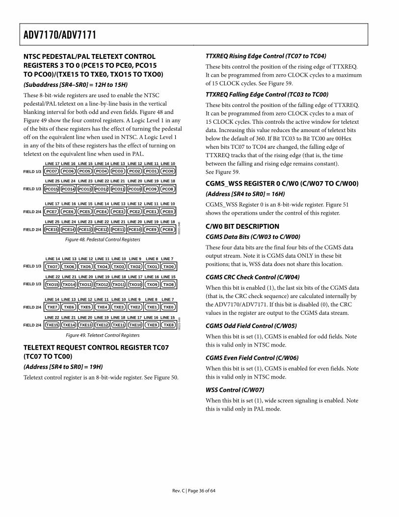
ADV7170/ADV7171
Rev. C | Page 36 of 64
NTSC PEDESTAL/PAL TELETEXT CONTROL REGISTERS 3 TO 0 (PCE15 TO PCE0, PCO15 TO PCO0)/(TXE15 TO TXE0, TXO15 TO TXO0) (Subaddress [SR4–SR0] = 12H to 15H)
These 8-bit-wide registers are used to enable the NTSC pedestal/PAL teletext on a line-by-line basis in the vertical blanking interval for both odd and even fields. Figure 48 and Figure 49 show the four control registers. A Logic Level 1 in any of the bits of these registers has the effect of turning the pedestal off on the equivalent line when used in NTSC. A Logic Level 1 in any of the bits of these registers has the effect of turning on teletext on the equivalent line when used in PAL.
FIELD 1/3 PCO6 PCO5 PCO3 PCO1PCO4 PCO2 PCO0PCO7
LINE 17 LINE 16 LINE 15 LINE 14 LINE 13 LINE 12 LINE 11 LINE 10
PCO14 PCO13 PCO11 PCO9PCO12 PCO10 PCO8PCO15
LINE 25 LINE 24 LINE 23 LINE 22 LINE 21 LINE 20 LINE 19 LINE 18
FIELD 1/3
FIELD 2/4 PCE6 PCE5 PCE3 PCE1PCE4 PCE2 PCE0PCE7
LINE 17 LINE 16 LINE 15 LINE 14 LINE 13 LINE 12 LINE 11 LINE 10
PCE14 PCE13 PCE11 PCE9PCE12 PCE10 PCE8PCE15
LINE 25 LINE 24 LINE 23 LINE 22 LINE 21 LINE 20 LINE 19 LINE 18
FIELD 2/4
0022
1-04
8
Figure 48. Pedestal Control Registers
FIELD 1/3
FIELD 1/3
FIELD 2/4
FIELD 2/4
TXO6 TXO5 TXO3 TXO1TXO4 TXO2 TXO0TXO7
LINE 14 LINE 13 LINE 12 LINE 11 LINE 10 LINE 9 LINE 8 LINE 7
TXO14 TXO13 TXO11 TXO9TXO12 TXO10 TXO8TXO15
LINE 22 LINE 21 LINE 20 LINE 19 LINE 18 LINE 17 LINE 16 LINE 15
TXE6 TXE5 TXE3 TXE1TXE4 TXE2 TXE0TXE7
TXE14 TXE13 TXE11 TXE9TXE12 TXE10 TXE8TXE15
LINE 14 LINE 13 LINE 12 LINE 11 LINE 10 LINE 9 LINE 8 LINE 7
LINE 22 LINE 21 LINE 20 LINE 19 LINE 18 LINE 17 LINE 16 LINE 15
0022
1-04
9
Figure 49. Teletext Control Registers
TELETEXT REQUEST CONTROL REGISTER TC07 (TC07 TO TC00) (Address [SR4 to SR0] = 19H)
Teletext control register is an 8-bit-wide register. See Figure 50.
TTXREQ Rising Edge Control (TC07 to TC04)
These bits control the position of the rising edge of TTXREQ. It can be programmed from zero CLOCK cycles to a maximum of 15 CLOCK cycles. See Figure 59.
TTXREQ Falling Edge Control (TC03 to TC00)
These bits control the position of the falling edge of TTXREQ. It can be programmed from zero CLOCK cycles to a max of 15 CLOCK cycles. This controls the active window for teletext data. Increasing this value reduces the amount of teletext bits below the default of 360. If Bit TC03 to Bit TC00 are 00Hex when bits TC07 to TC04 are changed, the falling edge of TTXREQ tracks that of the rising edge (that is, the time between the falling and rising edge remains constant). See Figure 59.
CGMS_WSS REGISTER 0 C/W0 (C/W07 TO C/W00) (Address [SR4 to SR0] = 16H)
CGMS_WSS Register 0 is an 8-bit-wide register. Figure 51 shows the operations under the control of this register.
C/W0 BIT DESCRIPTION CGMS Data Bits (C/W03 to C/W00)
These four data bits are the final four bits of the CGMS data output stream. Note it is CGMS data ONLY in these bit positions; that is, WSS data does not share this location.
CGMS CRC Check Control (C/W04)
When this bit is enabled (1), the last six bits of the CGMS data (that is, the CRC check sequence) are calculated internally by the ADV7170/ADV7171. If this bit is disabled (0), the CRC values in the register are output to the CGMS data stream.
CGMS Odd Field Control (C/W05)
When this bit is set (1), CGMS is enabled for odd fields. Note this is valid only in NTSC mode.
CGMS Even Field Control (C/W06)
When this bit is set (1), CGMS is enabled for even fields. Note this is valid only in NTSC mode.
WSS Control (C/W07)
When this bit is set (1), wide screen signaling is enabled. Note this is valid only in PAL mode.
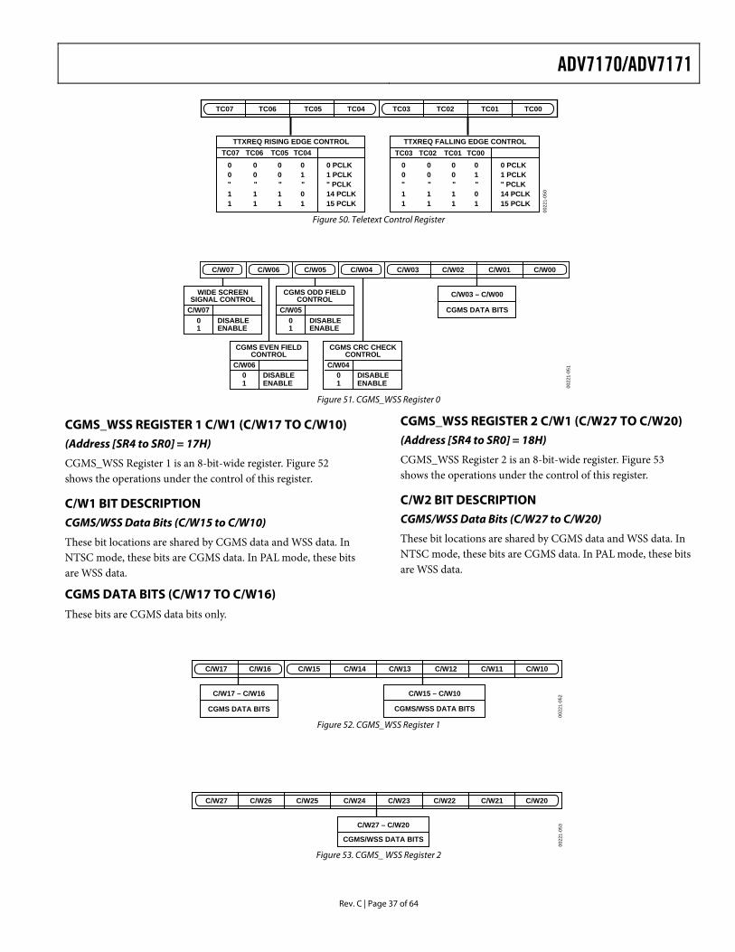
ADV7170/ADV7171
Rev. C | Page 37 of 64
TC01 TC00TC07 TC02TC04 TC03TC05TC06
TTXREQ RISING EDGE CONTROLTC07 TC06 TC05 TC04
0 0 0 0 0 PCLK0 0 0 1 1 PCLK" " " " " PCLK1 1 1 0 14 PCLK1 1 1 1 15 PCLK
TTXREQ FALLING EDGE CONTROLTC03 TC02 TC01 TC00
0 0 0 0 0 PCLK0 0 0 1 1 PCLK" " " " " PCLK1 1 1 0 14 PCLK1 1 1 1 15 PCLK
0022
1-05
0
Figure 50. Teletext Control Register
C/W07 C/W06 C/W05 C/W04 C/W03 C/W02 C/W01 C/W00
C/W07
WIDE SCREENSIGNAL CONTROL
0 DISABLE1 ENABLE
0 DISABLE1 ENABLE
C/W05
CGMS ODD FIELDCONTROL
C/W06
CGMS EVEN FIELDCONTROL
0 DISABLE1 ENABLE
C/W04
CGMS CRC CHECKCONTROL
0 DISABLE1 ENABLE
C/W03 – C/W00
CGMS DATA BITS
0022
1-05
1
Figure 51. CGMS_WSS Register 0
CGMS_WSS REGISTER 1 C/W1 (C/W17 TO C/W10) (Address [SR4 to SR0] = 17H)
CGMS_WSS Register 1 is an 8-bit-wide register. Figure 52 shows the operations under the control of this register.
C/W1 BIT DESCRIPTION CGMS/WSS Data Bits (C/W15 to C/W10)
These bit locations are shared by CGMS data and WSS data. In NTSC mode, these bits are CGMS data. In PAL mode, these bits are WSS data.
CGMS DATA BITS (C/W17 TO C/W16) These bits are CGMS data bits only.
CGMS_WSS REGISTER 2 C/W1 (C/W27 TO C/W20) (Address [SR4 to SR0] = 18H)
CGMS_WSS Register 2 is an 8-bit-wide register. Figure 53 shows the operations under the control of this register.
C/W2 BIT DESCRIPTION CGMS/WSS Data Bits (C/W27 to C/W20)
These bit locations are shared by CGMS data and WSS data. In NTSC mode, these bits are CGMS data. In PAL mode, these bits are WSS data.
C/W17 C/W16 C/W15 C/W14 C/W13 C/W12 C/W11 C/W10
C/W15 – C/W10
CGMS/WSS DATA BITS
C/W17 – C/W16
CGMS DATA BITS
0022
1-05
2
Figure 52. CGMS_WSS Register 1
C/W27 C/W26 C/W25 C/W24 C/W23 C/W22 C/W21 C/W20
C/W27 – C/W20
CGMS/WSS DATA BITS
0022
1-05
3
Figure 53. CGMS_ WSS Register 2
ADV7170/ADV7171
Rev. C | Page 38 of 64
APPENDICES APPENDIX 1—BOARD DESIGN AND LAYOUT CONSIDERATIONS The ADV7170/ADV7171 are highly integrated circuits containing both precision analog and high speed digital circuitry. They have been designed to minimize interference effects of the high speed digital circuitry on the integrity of the analog circuitry. It is imperative that these same design and layout techniques be applied to the system level design so that high speed, accurate performance is achieved. Figure 54 shows the analog interface between the device and monitor.
The layout should be optimized for lowest noise on the ADV7170/ADV7171 power and ground lines by shielding the digital inputs and providing good decoupling. The lead length between groups of VAA and GND pins should be minimized to minimize inductive ringing.
Ground Planes
The ground plane should encompass all ADV7170/ADV7171 ground pins, voltage reference circuitry, power supply bypass circuitry for the ADV7170/ADV7171, the analog output traces, and all the digital signal traces leading up to the ADV7170/ ADV7171. The ground plane is the board’s common ground plane.
Power Planes
The ADV7170, the ADV7171, and any associated analog circuitry should each have its own power plane, referred to as the analog power plane (VAA). This power plane should be connected to the regular PCB power plane (VCC) at a single point through a ferrite bead. This bead should be located within three inches of the ADV7170/ADV7171.
The metallization gap separating device power plane and board power plane should be as narrow as possible to minimize the obstruction to the flow of heat from the device into the general board.
The PCB power plane should provide power to all digital logic on the PC board, and the analog power plane should provide power to all ADV7170/ADV7171 power pins and voltage reference circuitry.
Plane-to-plane noise coupling can be reduced by ensuring that portions of the regular PCB power and ground planes do not overlay portions of the analog power plane unless they can be arranged so that the plane-to-plane noise is common-mode.
Supply Decoupling
For optimum performance, bypass capacitors should be installed using the shortest leads possible, consistent with reliable operation, to reduce the lead inductance. Best performance is obtained with 0.1 μF ceramic capacitor decoupling. Each group of VAA pins on the ADV7170/ ADV7171 must have at least one 0.1 μF decoupling capacitor to GND. These capacitors should be placed as close as possible to the device.
It is important to note that while the ADV7170/ADV7171 contain circuitry to reject power supply noise, this rejection decreases with frequency. If a high frequency switching power supply is used, the designer should pay close attention to reducing power supply noise and consider using a three-terminal voltage regulator for supplying power to the analog power plane.
Digital Signal Interconnect
The digital inputs to the ADV7170/ADV7171 should be isolated as much as possible from the analog outputs and other analog circuitry. Also, these input signals should not overlay the analog power plane.
Due to the high clock rates involved, long clock lines to the ADV7170/ADV7171 should be avoided to reduce noise pickup.
Any active termination resistors for the digital inputs should be connected to the regular PCB power plane (VCC) and not to the analog power plane.
Analog Signal Interconnect
The ADV7170/ADV7171 should be located as close as possible to the output connectors to minimize noise pickup and reflections due to impedance mismatch.
The video output signals should overlay the ground plane, not the analog power plane, to maximize the high frequency power supply rejection.
Digital inputs, especially pixel data inputs and clocking signals, should never overlay any of the analog signal circuitry and should be kept as far away as possible.
For best performance, the outputs should each have a 75 Ω load resistor connected to GND. These resistors should be placed as close as possible to the ADV7170/ADV7171 to minimize reflections.
The ADV7170/ADV7171 should have no inputs left floating. Any inputs that are not required should be tied to ground.

ADV7170/ADV7171
Rev. C | Page 39 of 64
75Ω
75Ω
75Ω
75Ω
150Ω
5kΩ 5kΩ
5V (VCC) 5V (VCC)
100Ω
100Ω MPU BUS
10, 19, 21,29, 43
27DAC D
26DAC C
31DAC B
32DAC A
23SCLOCK
24SDATA
34RSET
1, 11, 20, 28, 30
VAA
ADV7170/ADV7171
25 COMP
33 VREF
35 SCRESET/RTC
15 HSYNC
16 FIELD/VSYNC
17 BLANK
22 RESET
37 TTX
36 TTXREQ
44 CLOCK
P15–P0
38–42,2–9, 12–14
18ALSB GND
5V (VAA)5V (VAA)
0.1μF0.1μF
UNUSEDINPUTS
SHOULD BEGROUNDED
10kΩ
5V (VAA)
27MHz CLOCK(SAME CLOCK AS USED BY
MPEG2 DECODER)
TELETEXT PULL-UP ANDPULL-DOWN RESISTORSSHOULD ONLY BE USEDIF THESE PINS ARE NOTCONNECTED
100nF
5V (VAA)
4kΩ
5V (VCC)
100kΩ
100kΩ
RESET
TTX
TTXREQ
POWER SUPPLY DECOUPLINGFOR EACH POWER SUPPLY GROUP
0.1μF 0.01μF
10μF
5V (VAA)L1
(FERRITE BEAD)
33μF5VVCCGND
S-VIDEO
0022
1-05
4
Figure 54. Recommended Analog Circuit Layout
The circuit in Figure 55 can be used to generate a 13.5 MHz waveform using the 27 MHz clock and the HSYNC pulse. This waveform is guaranteed to produce the 13.5 MHz clock in synchronization with the 27 MHz clock. This 13.5 MHz clock can be used if a 13.5 MHz clock is required by the MPEG decoder. This guarantees that the Cr and Cb pixel information is input to the ADV7170/ADV7171 in the correct sequence.
D Q
CK
D Q
CKCLOCK
HSYNC
13.5MHz
0022
1-05
5
Figure 55. Circuit to Generate 13.5 MHz
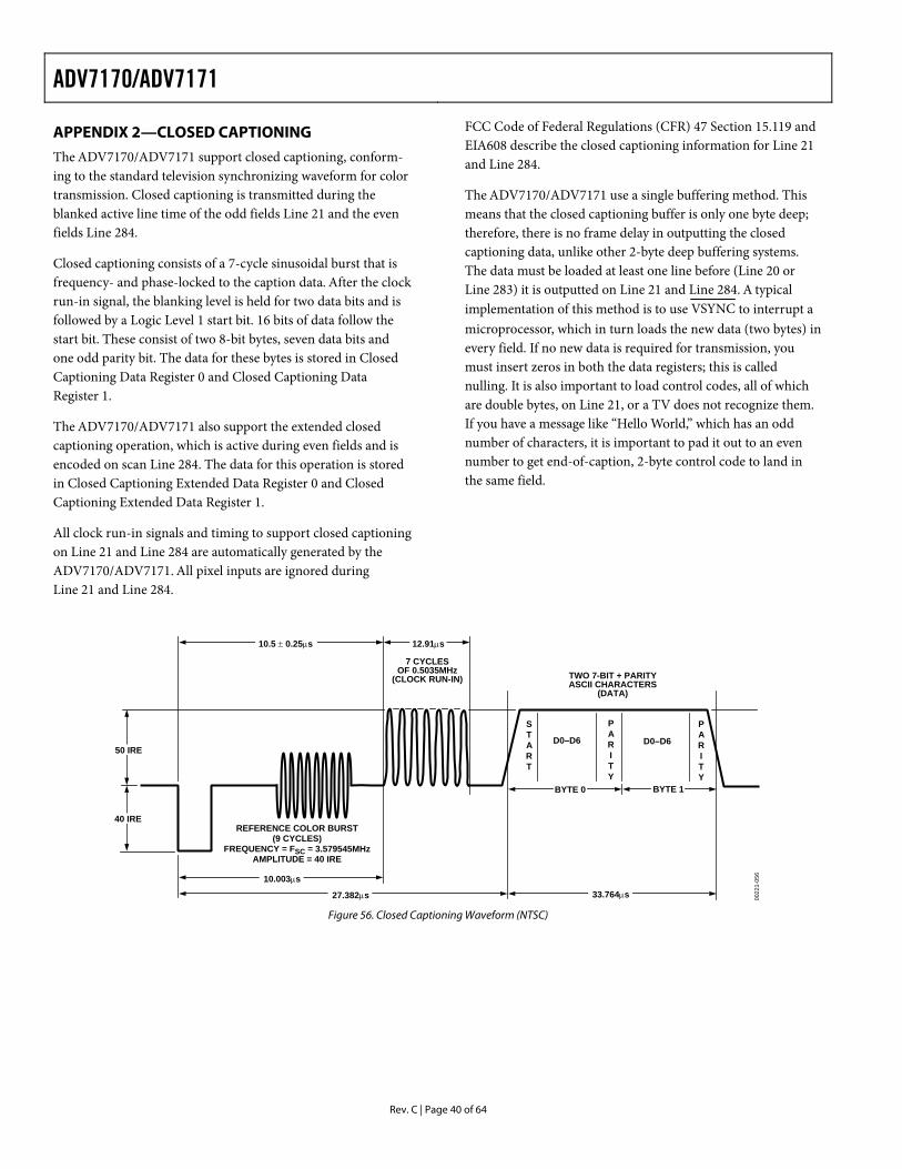
ADV7170/ADV7171
Rev. C | Page 40 of 64
APPENDIX 2—CLOSED CAPTIONING The ADV7170/ADV7171 support closed captioning, conform-ing to the standard television synchronizing waveform for color transmission. Closed captioning is transmitted during the blanked active line time of the odd fields Line 21 and the even fields Line 284.
Closed captioning consists of a 7-cycle sinusoidal burst that is frequency- and phase-locked to the caption data. After the clock run-in signal, the blanking level is held for two data bits and is followed by a Logic Level 1 start bit. 16 bits of data follow the start bit. These consist of two 8-bit bytes, seven data bits and one odd parity bit. The data for these bytes is stored in Closed Captioning Data Register 0 and Closed Captioning Data Register 1.
The ADV7170/ADV7171 also support the extended closed captioning operation, which is active during even fields and is encoded on scan Line 284. The data for this operation is stored in Closed Captioning Extended Data Register 0 and Closed Captioning Extended Data Register 1.
All clock run-in signals and timing to support closed captioning on Line 21 and Line 284 are automatically generated by the ADV7170/ADV7171. All pixel inputs are ignored during Line 21 and Line 284.
FCC Code of Federal Regulations (CFR) 47 Section 15.119 and EIA608 describe the closed captioning information for Line 21 and Line 284.
The ADV7170/ADV7171 use a single buffering method. This means that the closed captioning buffer is only one byte deep; therefore, there is no frame delay in outputting the closed captioning data, unlike other 2-byte deep buffering systems. The data must be loaded at least one line before (Line 20 or Line 283) it is outputted on Line 21 and Line 284. A typical implementation of this method is to use VSYNC to interrupt a microprocessor, which in turn loads the new data (two bytes) in every field. If no new data is required for transmission, you must insert zeros in both the data registers; this is called nulling. It is also important to load control codes, all of which are double bytes, on Line 21, or a TV does not recognize them. If you have a message like “Hello World,” which has an odd number of characters, it is important to pad it out to an even number to get end-of-caption, 2-byte control code to land in the same field.
START
PARITY
PARITY
D0–D6 D0–D6
10.003μs
33.764μs
50 IRE
40 IREREFERENCE COLOR BURST
(9 CYCLES)FREQUENCY = FSC = 3.579545MHz
AMPLITUDE = 40 IRE
7 CYCLESOF 0.5035MHz
(CLOCK RUN-IN)
10.5 ± 0.25μs
TWO 7-BIT + PARITYASCII CHARACTERS
(DATA)
27.382μs
BYTE 0 BYTE 1
0022
1-05
6
12.91μs
Figure 56. Closed Captioning Waveform (NTSC)
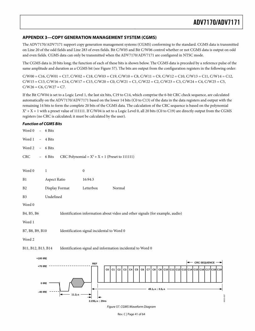
ADV7170/ADV7171
Rev. C | Page 41 of 64
APPENDIX 3—COPY GENERATION MANAGEMENT SYSTEM (CGMS) The ADV7170/ADV7171 support copy generation management systems (CGMS) conforming to the standard. CGMS data is transmitted on Line 20 of the odd fields and Line 283 of even fields. Bit C/W05 and Bit C/W06 control whether or not CGMS data is output on odd and even fields. CGMS data can only be transmitted when the ADV7170/ADV7171 are configured in NTSC mode.
The CGMS data is 20 bits long; the function of each of these bits is shown below. The CGMS data is preceded by a reference pulse of the same amplitude and duration as a CGMS bit (see Figure 57). The bits are output from the configuration registers in the following order:
C/W00 = C16, C/W01 = C17, C/W02 = C18, C/W03 = C19, C/W10 = C8, C/W11 = C9, C/W12 = C10, C/W13 = C11, C/W14 = C12, C/W15 = C13, C/W16 = C14, C/W17 = C15, C/W20 = C0, C/W21 = C1, C/W22 = C2, C/W23 = C3, C/W24 = C4, C/W25 = C5, C/W26 = C6, C/W27 = C7.
If the Bit C/W04 is set to a Logic Level 1, the last six bits, C19 to C14, which comprise the 6-bit CRC check sequence, are calculated automatically on the ADV7170/ADV7171 based on the lower 14 bits (C0 to C13) of the data in the data registers and output with the remaining 14 bits to form the complete 20 bits of the CGMS data. The calculation of the CRC sequence is based on the polynomial X6 + X + 1 with a preset value of 111111. If C/W04 is set to a Logic Level 0, all 20 bits (C0 to C19) are directly output from the CGMS registers (no CRC is calculated; it must be calculated by the user).
Function of CGMS Bits
Word 0 – 6 Bits
Word 1 – 4 Bits
Word 2 – 6 Bits
CRC – 6 Bits CRC Polynomial = X6 + X + 1 (Preset to 111111)
Word 0 1 0
B1 Aspect Ratio 16:94:3
B2 Display Format Letterbox Normal
B3 Undefined
Word 0
B4, B5, B6 Identification information about video and other signals (for example, audio)
Word 1
B7, B8, B9, B10 Identification signal incidental to Word 0
Word 2
B11, B12, B13, B14 Identification signal and information incidental to Word 0
CRC SEQUENCE
49.1μs ± 0.5μs
11.2μs
2.235μs ± 20ns
REF
C0 C1 C2 C3 C4 C5 C6 C7 C8 C9 C10 C11 C12 C13 C14 C15 C16 C17 C18 C19
+100 IRE
+70 IRE
0 IRE
–40 IRE
0022
1-05
7
Figure 57. CGMS Waveform Diagram
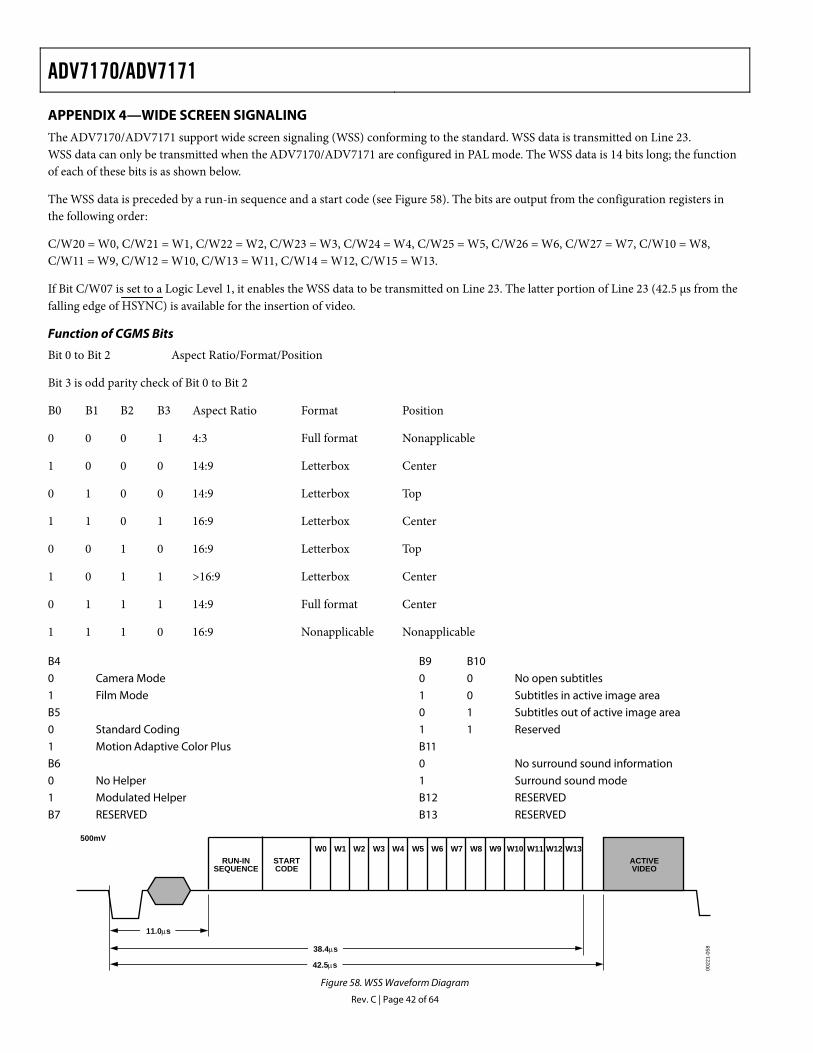
ADV7170/ADV7171
Rev. C | Page 42 of 64
APPENDIX 4—WIDE SCREEN SIGNALING The ADV7170/ADV7171 support wide screen signaling (WSS) conforming to the standard. WSS data is transmitted on Line 23. WSS data can only be transmitted when the ADV7170/ADV7171 are configured in PAL mode. The WSS data is 14 bits long; the function of each of these bits is as shown below.
The WSS data is preceded by a run-in sequence and a start code (see Figure 58). The bits are output from the configuration registers in the following order:
C/W20 = W0, C/W21 = W1, C/W22 = W2, C/W23 = W3, C/W24 = W4, C/W25 = W5, C/W26 = W6, C/W27 = W7, C/W10 = W8, C/W11 = W9, C/W12 = W10, C/W13 = W11, C/W14 = W12, C/W15 = W13.
If Bit C/W07 is set to a Logic Level 1, it enables the WSS data to be transmitted on Line 23. The latter portion of Line 23 (42.5 μs from the falling edge of HSYNC) is available for the insertion of video.
Function of CGMS Bits
Bit 0 to Bit 2 Aspect Ratio/Format/Position
Bit 3 is odd parity check of Bit 0 to Bit 2
B0 B1 B2 B3 Aspect Ratio Format Position
0 0 0 1 4:3 Full format Nonapplicable
1 0 0 0 14:9 Letterbox Center
0 1 0 0 14:9 Letterbox Top
1 1 0 1 16:9 Letterbox Center
0 0 1 0 16:9 Letterbox Top
1 0 1 1 >16:9 Letterbox Center
0 1 1 1 14:9 Full format Center
1 1 1 0 16:9 Nonapplicable Nonapplicable
B4 0 Camera Mode 1 Film Mode B5 0 Standard Coding 1 Motion Adaptive Color Plus B6 0 No Helper 1 Modulated Helper B7 RESERVED
B9 B10 0 0 No open subtitles 1 0 Subtitles in active image area 0 1 Subtitles out of active image area 1 1 Reserved B11 0 No surround sound information 1 Surround sound mode B12 RESERVED B13 RESERVED
11.0μs
W0 W1 W2 W3 W4 W5 W6 W7 W8 W9 W10 W11 W12 W13500mV
RUN-INSEQUENCE
STARTCODE
ACTIVEVIDEO
38.4μs
42.5μs 0022
1-05
8
Figure 58. WSS Waveform Diagram
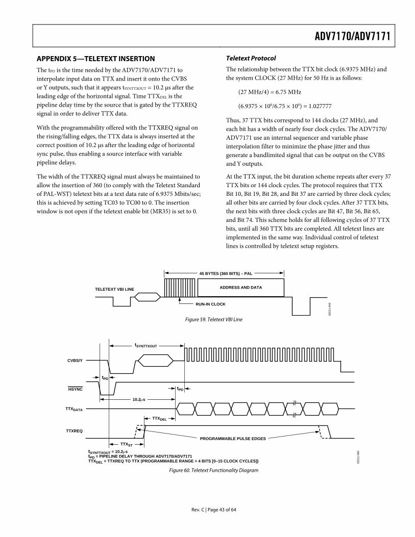
ADV7170/ADV7171
Rev. C | Page 43 of 64
APPENDIX 5—TELETEXT INSERTION The tPD is the time needed by the ADV7170/ADV7171 to interpolate input data on TTX and insert it onto the CVBS or Y outputs, such that it appears tSYNTTXOUT = 10.2 μs after the leading edge of the horizontal signal. Time TTXDEL is the pipeline delay time by the source that is gated by the TTXREQ signal in order to deliver TTX data.
With the programmability offered with the TTXREQ signal on the rising/falling edges, the TTX data is always inserted at the correct position of 10.2 μs after the leading edge of horizontal sync pulse, thus enabling a source interface with variable pipeline delays.
The width of the TTXREQ signal must always be maintained to allow the insertion of 360 (to comply with the Teletext Standard of PAL-WST) teletext bits at a text data rate of 6.9375 Mbits/sec; this is achieved by setting TC03 to TC00 to 0. The insertion window is not open if the teletext enable bit (MR35) is set to 0.
Teletext Protocol
The relationship between the TTX bit clock (6.9375 MHz) and the system CLOCK (27 MHz) for 50 Hz is as follows:
(27 MHz/4) = 6.75 MHz
(6.9375 × 10⁶/6.75 × 106) = 1.027777
Thus, 37 TTX bits correspond to 144 clocks (27 MHz), and each bit has a width of nearly four clock cycles. The ADV7170/ ADV7171 use an internal sequencer and variable phase interpolation filter to minimize the phase jitter and thus generate a bandlimited signal that can be output on the CVBS and Y outputs.
At the TTX input, the bit duration scheme repeats after every 37 TTX bits or 144 clock cycles. The protocol requires that TTX Bit 10, Bit 19, Bit 28, and Bit 37 are carried by three clock cycles; all other bits are carried by four clock cycles. After 37 TTX bits, the next bits with three clock cycles are Bit 47, Bit 56, Bit 65, and Bit 74. This scheme holds for all following cycles of 37 TTX bits, until all 360 TTX bits are completed. All teletext lines are implemented in the same way. Individual control of teletext lines is controlled by teletext setup registers.
ADDRESS AND DATA
RUN-IN CLOCK
TELETEXT VBI LINE
45 BYTES (360 BITS) – PAL
0022
1-05
9
Figure 59. Teletext VBI Line
PROGRAMMABLE PULSE EDGES
tPD
tPD
CVBS/Y
HSYNC
TTXREQ
TTXDATA
tSYNTTXOUT
10.2μs
TTXDEL
TTXST
tSYNTTXOUT = 10.2μstPD = PIPELINE DELAY THROUGH ADV7170/ADV7171TTXDEL = TTXREQ TO TTX (PROGRAMMABLE RANGE = 4 BITS [0–15 CLOCK CYCLES]) 00
221-
060
Figure 60. Teletext Functionality Diagram

ADV7170/ADV7171
Rev. C | Page 44 of 64
APPENDIX 6—WAVEFORMS NTSC Waveforms (with Pedestal)
+130.8 IRE
+100 IRE
+7.5 IRE0 IRE
–40 IRE
PEAK COMPOSITE
REF WHITE
BLACK LEVEL
SYNC LEVEL
BLANK LEVEL
714.2mV
1268.1mV
1048.4mV
387.6mV334.2mV
48.3mV 0022
1-06
1
Figure 61. NTSC Composite Video Levels
+100 IRE
+7.5 IRE0 IRE
–40 IRE
REF WHITE
BLACK LEVEL
SYNC LEVEL
BLANK LEVEL
714.2mV
1048.4mV
387.6mV334.2mV
48.3mV 0022
1-06
2
Figure 62. NTSC Luma Video Levels
650mV
335.2mV
963.8mV
0mV
PEAK CHROMA
BLANK/BLACK LEVEL286mV p-p
629.7mV p-p
PEAK CHROMA00
221-
063
Figure 63. NTSC Chroma Video Levels
+100 IRE
+7.5 IRE0 IRE
–40 IRE
REF WHITE
BLACK LEVEL
SYNC LEVEL
BLANK LEVEL
720.8mV
1052.2mV
387.5mV331.4mV
45.9mV 0022
1-06
4
Figure 64. NTSC RGB Video Levels
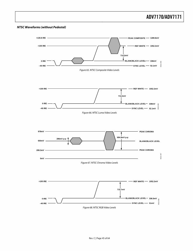
ADV7170/ADV7171
Rev. C | Page 45 of 64
NTSC Waveforms (without Pedestal)
+130.8 IRE
+100 IRE
0 IRE
–40 IRE
PEAK COMPOSITE
REF WHITE
SYNC LEVEL
BLANK/BLACK LEVEL
714.2mV
1289.8mV
1052.2mV
338mV
52.1mV 0022
1-06
5
Figure 65. NTSC Composite Video Levels
+100 IRE
0 IRE
–40 IRE
REF WHITE
SYNC LEVEL
BLANK/BLACK LEVEL
714.2mV
1052.2mV
338mV
52.1mV 0022
1-06
6
Figure 66. NTSC Luma Video Levels
650mV
299.3mV
978mV
0mV
PEAK CHROMA
BLANK/BLACK LEVEL286mV p-p
PEAK CHROMA
694.9mV p-p
0022
1-06
7
Figure 67. NTSC Chroma Video Levels
+100 IRE
0 IRE
–40 IRE
REF WHITE
SYNC LEVEL
BLANK/BLACK LEVEL
715.7mV
1052.2mV
336.5mV
51mV 0022
1-06
8
Figure 68. NTSC RGB Video Levels

ADV7170/ADV7171
Rev. C | Page 46 of 64
PAL Waveforms
1284.2mV
1047.1mV
350.7mV
50.8mV
PEAK COMPOSITE
REF WHITE
SYNC LEVEL
BLANK/BLACK LEVEL
696.4mV
0022
1-06
9
Figure 69. PAL Composite Video Levels
1047mV
350.7mV
50.8mV
REF WHITE
SYNC LEVEL
BLANK/BLACK LEVEL
696.4mV
0022
1-07
0
Figure 70. PAL Luma Video Levels
650mV
317.7mV
989.7mV
0mV
PEAK CHROMA
BLANK/BLACK LEVEL300mV p-p 672mV p-p
PEAK CHROMA
0022
1-07
1
Figure 71. PAL Chroma Video Levels
1050.2mV
351.8mV
51mV
REF WHITE
SYNC LEVEL
BLANK/BLACK LEVEL
698.4mV
0022
1-07
2
Figure 72. PAL RGB Video Levels
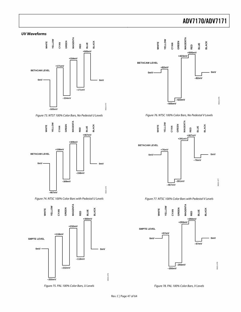
ADV7170/ADV7171
Rev. C | Page 47 of 64
UV Waveforms
BETACAM LEVEL
0mV
+171mV
+334mV
+505mV
0mV
–171mV
–334mV
–505mV
WH
ITE
YELL
OW
CYA
N
GR
EEN
MA
GEN
TA
RED
BLU
E
BLA
CK
0022
1-07
3
BETACAM LEVEL
0mV
+82mV
+423mV+505mV
0mV
–82mV
–505mV–423mV
WH
ITE
YELL
OW
CYA
N
GR
EEN
MA
GEN
T A
RED
BLU
E
BLA
CK
0022
1-07
6
Figure 76. NTSC 100% Color Bars, No Pedestal V Levels Figure 73. NTST 100% Color Bars, No Pedestal U Levels
BETACAM LEVEL
0mV
+76mV
+391mV+467mV
0mV
–76mV
–467mV–391mV
WH
ITE
YELL
OW
CYA
N
GR
EEN
MA
GEN
TA
RED
BLU
E
BLA
CK
0022
1-07
7
BETACAM LEVEL
0mV
+158mV
+309mV
+467mV
0mV
–158mV
–309mV
–467mV
WH
ITE
YELL
OW
CYA
N
GR
EEN
MA
GEN
TA
RED
BLU
E
BLA
CK
0022
1-07
4
Figure 74. NTSC 100% Color Bars with Pedestal U Levels Figure 77. NTSC 100% Color Bars with Pedestal V Levels
SMPTE LEVEL
0mV
+118mV
+232mV
+350mV
0mV
–118mV
–232mV
–350mV
WH
ITE
YELL
OW
CYA
N
GR
EEN
MA
GEN
T A
RED
BLU
E
BLA
CK
0022
1-07
5
SMPTE LEVEL
0mV
+57mV
+293mV+350mV
0mV
–57mV
–350mV–293mV
WH
ITE
YELL
OW
CYA
N
GR
EEN
MA
GEN
T A
RED
BLU
E
BLA
CK
0022
1-07
8
Figure 75. PAL 100% Color Bars, U Levels Figure 78. PAL 100% Color Bars, V Levels

ADV7170/ADV7171
Rev. C | Page 48 of 64
APPENDIX 7—OPTIONAL OUTPUT FILTER If an output filter is required for the CVBS, Y, UV, Chroma, and RGB outputs of the ADV7170/ADV7171, the filter shown in Figure 79 can be used. Plots of the filter characteristics are shown in Figure 80. An output filter is not required if the outputs of the ADV7170/ADV7171 are connected to most analog monitors or analog TVs. However, if the output signals are applied to a system where sampling is used (for example, digital TVs), then a filter is required to prevent aliasing.
1.8μH
75R 270pF
22pF
330pF
FILTER I/P FILTER O/P00
221-
079
Figure 79. Output Filter
0
80100k 100M
0022
1-08
0
FREQUENCY (Hz)
MA
GN
ITU
DE
(dB
)
1M 10M
10
20
30
40
50
60
70
Figure 80. Output Filter Plot
APPENDIX 8—OPTIONAL DAC BUFFERING When external buffering of the ADV7170/ADV7171 DAC outputs is needed, the configuration in Figure 81 is recom-mended. This configuration shows the DAC outputs running at half (18 mA) their full current (36 mA) capability. This allows the ADV7170/ADV7171 to dissipate less power; the analog current is reduced by 50% with a RSET of 300 Ω and a RLOAD of 75 Ω. This mode is recommended for 3.3 V operation, because optimum performance is obtained from the DAC outputs at 18 mA with a VAA of 3.3 V. This buffer also adds extra isolation on the video outputs (see the buffer circuit in Figure 82).
When calculating absolute output full-scale current and voltage, use the following equations:
LOADOUTOUT RIV ×=
( )SET
REFOUT R
KVI ×=
VVconstant,K REF 235.12146.4 ==
ADV7170/ADV7171
VREF
DIGITALCORE
PIXELPORT
300ΩRSET
VAA
OUTPUTBUFFERDAC A
OUTPUTBUFFER
OUTPUTBUFFER
OUTPUTBUFFER
DAC C
DAC D
DAC B
CVBS
LUMA
CHROMA
CVBS
0022
1-08
1
Figure 81. Output DAC Buffering Configuration
VCC+
VCC–
OUTPUT TOTV MONITOR
INPUT/OPTIONAL
FILTER O/P
5
23
1
4
AD8061
0022
1-08
2
Figure 82. Recommended Output DAC Buffer
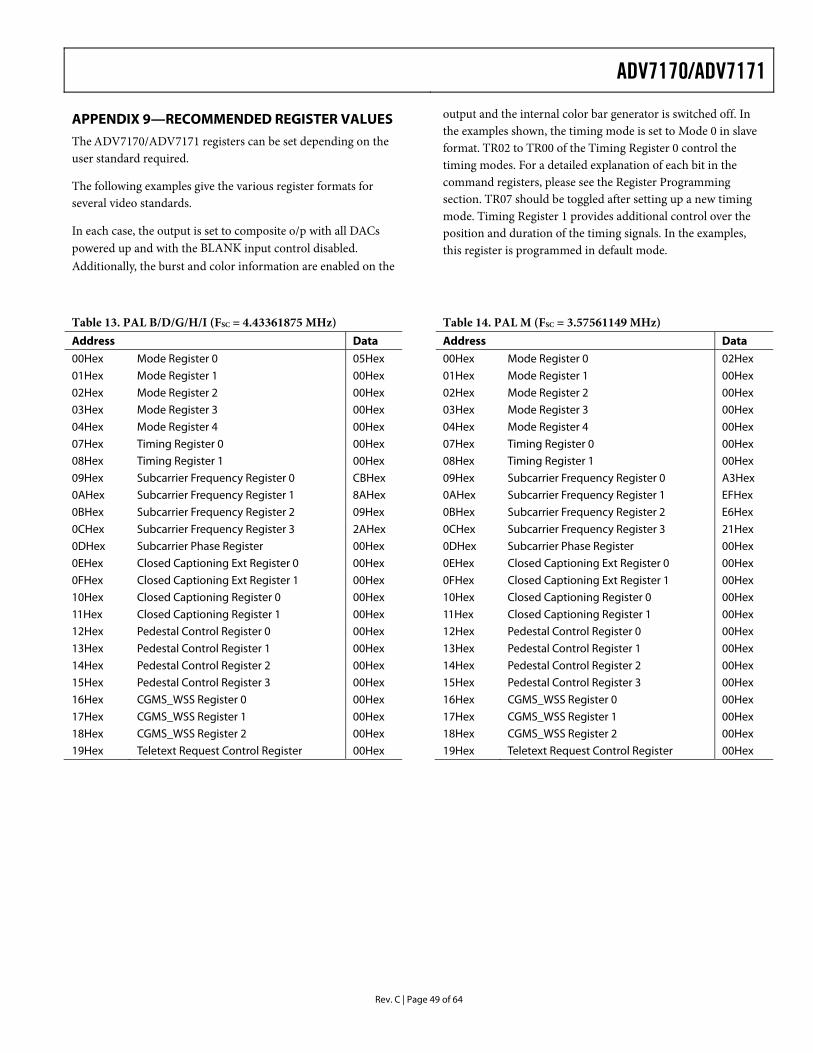
ADV7170/ADV7171
Rev. C | Page 49 of 64
APPENDIX 9—RECOMMENDED REGISTER VALUES The ADV7170/ADV7171 registers can be set depending on the user standard required.
The following examples give the various register formats for several video standards.
In each case, the output is set to composite o/p with all DACs powered up and with the BLANK input control disabled. Additionally, the burst and color information are enabled on the
output and the internal color bar generator is switched off. In the examples shown, the timing mode is set to Mode 0 in slave format. TR02 to TR00 of the Timing Register 0 control the timing modes. For a detailed explanation of each bit in the command registers, please see the section. TR07 should be toggled after setting up a new timing mode. Timing Register 1 provides additional control over the position and duration of the timing signals. In the examples, this register is programmed in default mode.
Register Programming
Table 13. PAL B/D/G/H/I (FSC = 4.43361875 MHz) Address Data 00Hex Mode Register 0 05Hex 01Hex Mode Register 1 00Hex 02Hex Mode Register 2 00Hex 03Hex Mode Register 3 00Hex 04Hex Mode Register 4 00Hex 07Hex Timing Register 0 00Hex 08Hex Timing Register 1 00Hex 09Hex Subcarrier Frequency Register 0 CBHex 0AHex Subcarrier Frequency Register 1 8AHex 0BHex Subcarrier Frequency Register 2 09Hex 0CHex Subcarrier Frequency Register 3 2AHex 0DHex Subcarrier Phase Register 00Hex 0EHex Closed Captioning Ext Register 0 00Hex 0FHex Closed Captioning Ext Register 1 00Hex 10Hex Closed Captioning Register 0 00Hex 11Hex Closed Captioning Register 1 00Hex 12Hex Pedestal Control Register 0 00Hex 13Hex Pedestal Control Register 1 00Hex 14Hex Pedestal Control Register 2 00Hex 15Hex Pedestal Control Register 3 00Hex 16Hex CGMS_WSS Register 0 00Hex 17Hex CGMS_WSS Register 1 00Hex 18Hex CGMS_WSS Register 2 00Hex 19Hex Teletext Request Control Register 00Hex
Table 14. PAL M (FSC = 3.57561149 MHz) Address Data 00Hex Mode Register 0 02Hex 01Hex Mode Register 1 00Hex 02Hex Mode Register 2 00Hex 03Hex Mode Register 3 00Hex 04Hex Mode Register 4 00Hex 07Hex Timing Register 0 00Hex 08Hex Timing Register 1 00Hex 09Hex Subcarrier Frequency Register 0 A3Hex 0AHex Subcarrier Frequency Register 1 EFHex 0BHex Subcarrier Frequency Register 2 E6Hex 0CHex Subcarrier Frequency Register 3 21Hex 0DHex Subcarrier Phase Register 00Hex 0EHex Closed Captioning Ext Register 0 00Hex 0FHex Closed Captioning Ext Register 1 00Hex 10Hex Closed Captioning Register 0 00Hex 11Hex Closed Captioning Register 1 00Hex 12Hex Pedestal Control Register 0 00Hex 13Hex Pedestal Control Register 1 00Hex 14Hex Pedestal Control Register 2 00Hex 15Hex Pedestal Control Register 3 00Hex 16Hex CGMS_WSS Register 0 00Hex 17Hex CGMS_WSS Register 1 00Hex 18Hex CGMS_WSS Register 2 00Hex 19Hex Teletext Request Control Register 00Hex
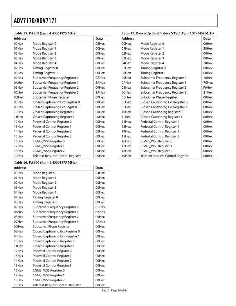
ADV7170/ADV7171
Rev. C | Page 50 of 64
Table 15. PAL N (FSC = 4.43361875 MHz) Address Data 00Hex Mode Register 0 05Hex 01Hex Mode Register 1 00Hex 02Hex Mode Register 2 00Hex 03Hex Mode Register 3 00Hex 04Hex Mode Register 4 00Hex 07Hex Timing Register 0 00Hex 08Hex Timing Register 1 00Hex 09Hex Subcarrier Frequency Register 0 CBHex 0AHex Subcarrier Frequency Register 1 8AHex 0BHex Subcarrier Frequency Register 2 09Hex 0CHex Subcarrier Frequency Register 3 2AHex 0DHex Subcarrier Phase Register 00Hex 0EHex Closed Captioning Ext Register 0 00Hex 0FHex Closed Captioning Ext Register 1 00Hex 10Hex Closed Captioning Register 0 00Hex 11Hex Closed Captioning Register 1 00Hex 12Hex Pedestal Control Register 0 00Hex 13Hex Pedestal Control Register 1 00Hex 14Hex Pedestal Control Register 2 00Hex 15Hex Pedestal Control Register 3 00Hex 16Hex CGMS_WSS Register 0 00Hex 17Hex CGMS_WSS Register 1 00Hex 18Hex CGMS_WSS Register 2 00Hex 19Hex Teletext Request Control Register 00Hex
Table 16. PAL60 (FSC = 4.43361875 MHz) Address Data 00Hex Mode Register 0 04Hex 01Hex Mode Register 1 00Hex 02Hex Mode Register 2 00Hex 03Hex Mode Register 3 00Hex 04Hex Mode Register 4 00Hex 07Hex Timing Register 0 00Hex 08Hex Timing Register 1 00Hex 09Hex Subcarrier Frequency Register 0 CBHex 0AHex Subcarrier Frequency Register 1 8AHex 0BHex Subcarrier Frequency Register 2 09Hex 0CHex Subcarrier Frequency Register 3 2AHex 0DHex Subcarrier Phase Register 00Hex 0EHex Closed Captioning Ext Register 0 00Hex 0FHex Closed Captioning Ext Register 1 00Hex 10Hex Closed Captioning Register 0 00Hex 11Hex Closed Captioning Register 1 00Hex 12Hex Pedestal Control Register 0 00Hex 13Hex Pedestal Control Register 1 00Hex 14Hex Pedestal Control Register 2 00Hex 15Hex Pedestal Control Register 3 00Hex 16Hex CGMS_WSS Register 0 00Hex 17Hex CGMS_WSS Register 1 00Hex 18Hex CGMS_WSS Register 2 00Hex 19Hex Teletext Request Control Register 00Hex
Table 17. Power-Up Reset Values NTSC (FSC = 3.5795454 MHz) Address Data 00Hex Mode Register 0 00Hex 01Hex Mode Register 1 58Hex 02Hex Mode Register 2 00Hex 03Hex Mode Register 3 00Hex 04Hex Mode Register 4 10Hex 07Hex Timing Register 0 00Hex 08Hex Timing Register 1 00Hex 09Hex Subcarrier Frequency Register 0 16Hex 0AHex Subcarrier Frequency Register 1 7CHex 0BHex Subcarrier Frequency Register 2 F0Hex 0CHex Subcarrier Frequency Register 3 21Hex 0DHex Subcarrier Phase Register 00Hex 0EHex Closed Captioning Ext Register 0 00Hex 0FHex Closed Captioning Ext Register 1 00Hex 10Hex Closed Captioning Register 0 00Hex 11Hex Closed Captioning Register 1 00Hex 12Hex Pedestal Control Register 0 00Hex 13Hex Pedestal Control Register 1 00Hex 14Hex Pedestal Control Register 2 00Hex 15Hex Pedestal Control Register 3 00Hex 16Hex CGMS_WSS Register 0 00Hex 17Hex CGMS_WSS Register 1 00Hex 18Hex CGMS_WSS Register 2 00Hex 19Hex Teletext Request Control Register 00Hex
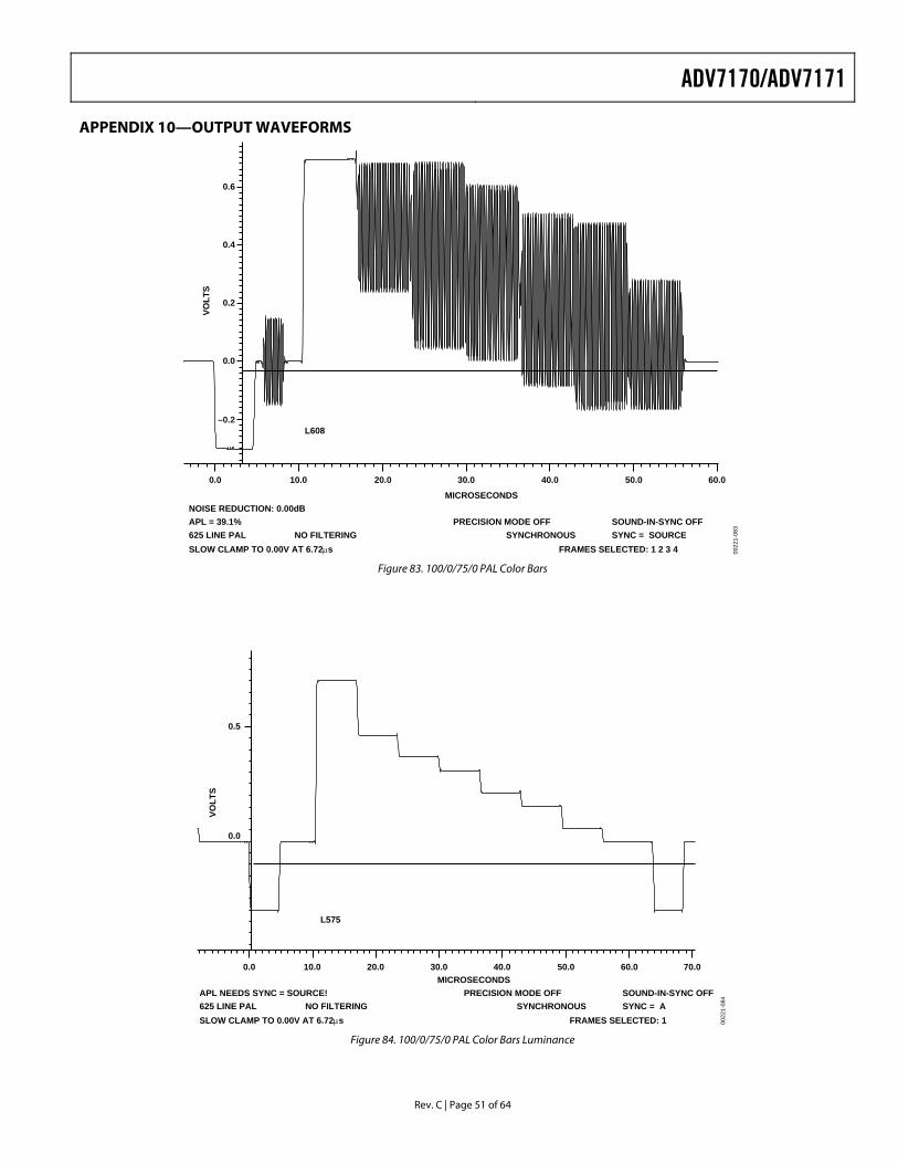
ADV7170/ADV7171
Rev. C | Page 51 of 64
APPENDIX 10—OUTPUT WAVEFORMS
0.6
0.4
0.2
0.0
–0.2L608
0.0 10.0 20.0 30.0 40.0 50.0 60.0
MICROSECONDSNOISE REDUCTION: 0.00dBAPL = 39.1% PRECISION MODE OFF SOUND-IN-SYNC OFF625 LINE PAL NO FILTERING SYNCHRONOUS SYNC = SOURCESLOW CLAMP TO 0.00V AT 6.72μs FRAMES SELECTED: 1 2 3 4
VOLT
S
0022
1-08
3
Figure 83. 100/0/75/0 PAL Color Bars
MICROSECONDSAPL NEEDS SYNC = SOURCE! PRECISION MODE OFF SOUND-IN-SYNC OFF625 LINE PAL NO FILTERING SYNCHRONOUS SYNC = ASLOW CLAMP TO 0.00V AT 6.72μs FRAMES SELECTED: 1
0.5
0.0
L575
0.0 10.0 20.0 30.0 40.0 50.0 60.0 70.0
VOLT
S
0022
1-08
4
Figure 84. 100/0/75/0 PAL Color Bars Luminance
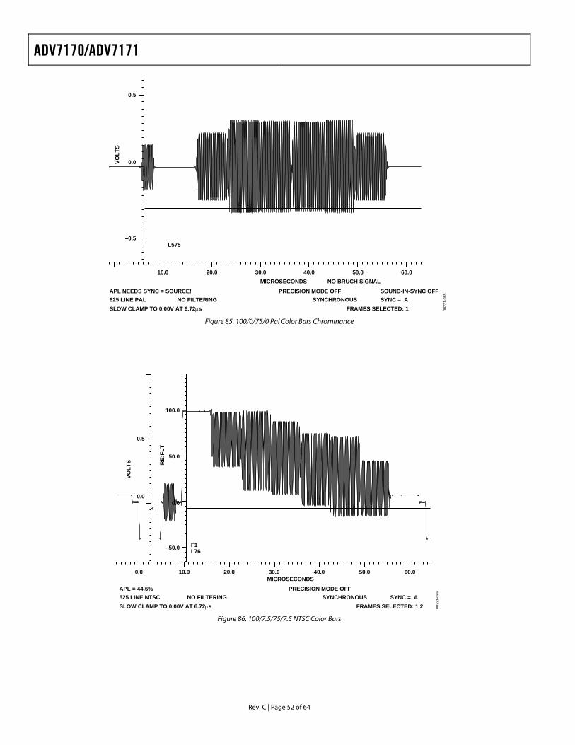
ADV7170/ADV7171
Rev. C | Page 52 of 64
APL NEEDS SYNC = SOURCE! PRECISION MODE OFF SOUND-IN-SYNC OFF625 LINE PAL NO FILTERING SYNCHRONOUS SYNC = ASLOW CLAMP TO 0.00V AT 6.72μs FRAMES SELECTED: 1
0.5
0.0
–0.5
10.0 30.0 40.0 50.0 60.020.0MICROSECONDS
L575
VOLT
S
NO BRUCH SIGNAL
0022
1-08
5
Figure 85. 100/0/75/0 Pal Color Bars Chrominance
APL = 44.6% PRECISION MODE OFF525 LINE NTSC NO FILTERING SYNCHRONOUS SYNC = ASLOW CLAMP TO 0.00V AT 6.72μs FRAMES SELECTED: 1 2
MICROSECONDS
0.5
0.0
–50.0
50.0
100.0
IRE:
FLT
VOLT
S
F1L76
0.0 10.0 20.0 30.0 40.0 50.0 60.0
0.0
0022
1-08
6
Figure 86. 100/7.5/75/7.5 NTSC Color Bars

ADV7170/ADV7171
Rev. C | Page 53 of 64
NOISE REDUCTION: 15.05dBAPL = 44.7% PRECISION MODE OFF525 LINE NTSC NO FILTERING SYNCHRONOUS SYNC = SOURCESLOW CLAMP TO 0.00V AT 6.72μs FRAMES SELECTED: 1 2
MICROSECONDS10.0 20.0 30.0 40.0 50.0 60.0
0.6
0.4
0.2
0.0
–0.2
50.0
0.0
IRE:
FLT
VOLT
S
F2L238
0022
1-08
7
Figure 87. 100/7.5/75/7.5 NTSC Color Bars Luminance
NOISE REDUCTION: 15.05dBAPL NEEDS SYNC = SOURCE! PRECISION MODE OFF525 LINE NTSC NO FILTERING SYNCHRONOUS SYNC = BSLOW CLAMP TO 0.00V AT 6.72μs FRAMES SELECTED: 1 2
MICROSECONDS0.0 10.0 20.0 30.0 40.0 50.0 60.0
0.4
0.2
0.0
–0.2
–0.4
VOLT
S
50.0
–50.0
F1L76
IRE:
FLT
0022
1-08
8
Figure 88. 100/7.5/75/7.5 NTSC Color Bars Chrominance
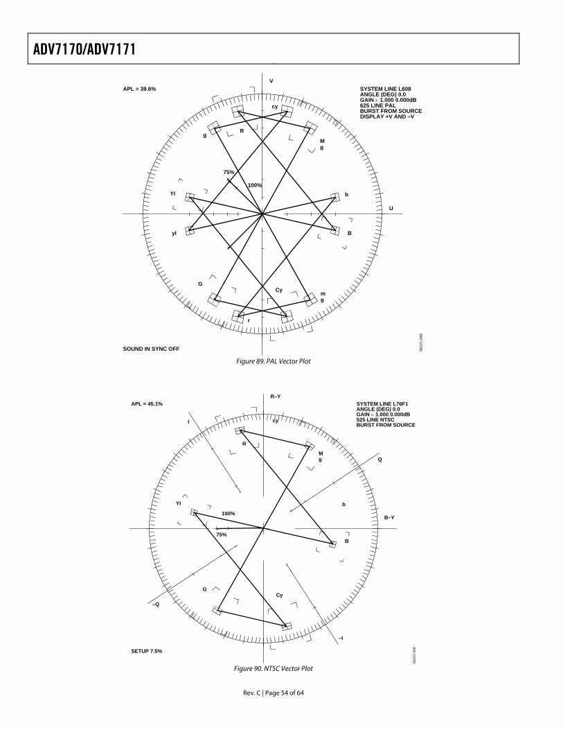
ADV7170/ADV7171
Rev. C | Page 54 of 64
APL = 39.6%
SOUND IN SYNC OFF
V
U
YI
yl
G
r
mg
Cy
Mg
cy
gR
75%
100%b
B
SYSTEM LINE L608ANGLE (DEG) 0.0GAIN × 1.000 0.000dB625 LINE PALBURST FROM SOURCEDISPLAY +V AND –V
0022
1-08
9
Figure 89. PAL Vector Plot
APL = 45.1%
SETUP 7.5%
R–Y
B–Y
YI
GCy
Mg
cyI
R
75%
100%
b
B
Q
–Q
–I
SYSTEM LINE L76F1ANGLE (DEG) 0.0GAIN × 1.000 0.000dB525 LINE NTSCBURST FROM SOURCE
0022
1-09
0
Figure 90. NTSC Vector Plot
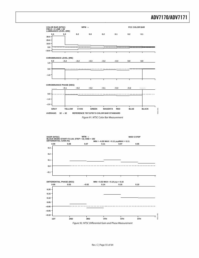
ADV7170/ADV7171
Rev. C | Page 55 of 64
COLOR BAR (NTSC)FIELD = 2 LINE = 28LUMINANCE LEVEL (IRE)
WFM → FCC COLOR BAR
0.4 0.2 0.2 0.0 0.2 0.1 0.2 0.1
0.0 –0.2 –0.2 –0.3 –0.2 –0.3 0.0 0.0
. . . . . –0.1 –0.2 –0.2 –0.1 –0.3 –0.2 - - - - -
CHROMINANCE LEVEL (IRE)
CHROMINANCE PHASE (DEG)
GRAY YELLOW CYAN GREEN MAGENTA RED BLUE BLACK
AVERAGE: 32 → 32 REFERENCE 75/7.5/75/7.5 COLOR BAR STANDARD
30.0
20.0
10.0
0.0
–10.0
1.0
0.0
–1.0
0.0
–1.0
–2.0
0022
1-09
1
Figure 91. NTSC Color Bar Measurement
DGDP (NTSC)BLOCK MODE START F2 L64, STEP = 32, END = 192DIFFERENTIAL GAIN (%)
WFM → MOD 5 STEP
MIN = –0.00 MAX = 0.11 p-p/MAX = 0.110.00 0.08 0.07 0.11 0.07 0.05
0.3
0.2
0.1
0.0
–0.1
0.20
0.15
0.10
0.05
–0.00
–0.05
–0.10
0.00 0.03 –0.02 0.14 0.10 0.10DIFFERENTIAL PHASE (DEG) MIN = 0.02 MAX = 0.14 p-p = 0.16
1ST 2ND 3RD 4TH 5TH 6TH 0022
1-09
2
Figure 92. NTSC Differential Gain and Phase Measurement
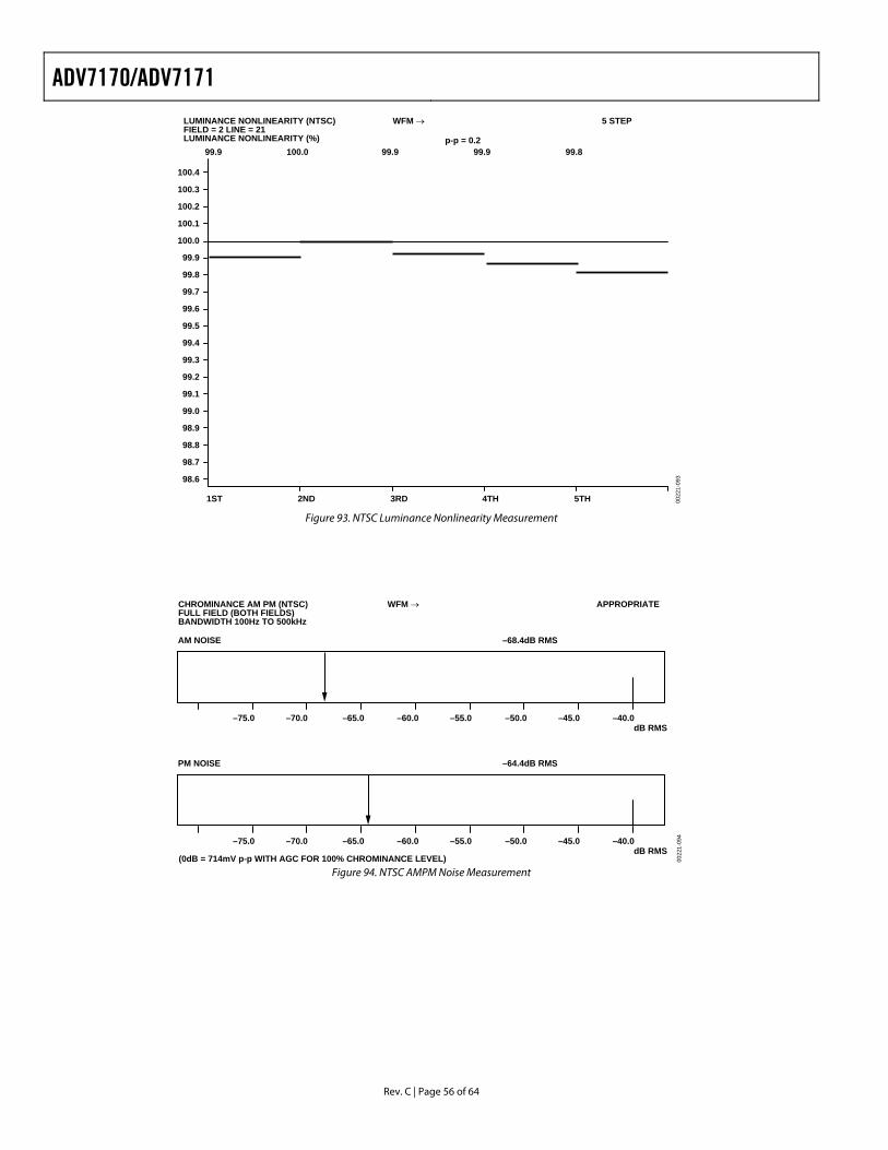
ADV7170/ADV7171
Rev. C | Page 56 of 64
LUMINANCE NONLINEARITY (NTSC)FIELD = 2 LINE = 21LUMINANCE NONLINEARITY (%)
WFM → 5 STEP
p-p = 0.299.9 100.0 99.9 99.9 99.8
100.4
100.3
100.2
100.1
100.0
99.9
99.8
99.7
99.6
99.5
99.4
99.3
99.2
99.1
99.0
98.9
98.8
98.7
98.6
1ST 2ND 3RD 4TH 5TH 0022
1-09
3
Figure 93. NTSC Luminance Nonlinearity Measurement
CHROMINANCE AM PM (NTSC)FULL FIELD (BOTH FIELDS)BANDWIDTH 100Hz TO 500kHz
WFM → APPROPRIATE
–75.0
AM NOISE –68.4dB RMS
–70.0 –65.0 –60.0 –55.0 –50.0 –45.0 –40.0dB RMS
–75.0
PM NOISE –64.4dB RMS
–70.0 –65.0 –60.0 –55.0 –50.0 –45.0 –40.0dB RMS
(0dB = 714mV p-p WITH AGC FOR 100% CHROMINANCE LEVEL) 0022
1-09
4
Figure 94. NTSC AMPM Noise Measurement
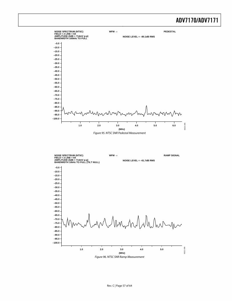
ADV7170/ADV7171
Rev. C | Page 57 of 64
NOISE SPECTRUM (NTSC)FIELD = 2 LINE = 64AMPLITUDE (0dB = 714mV p-p)BANDWIDTH 100kHz TO FULL
WFM → PEDESTAL
NOISE LEVEL = –80.1dB RMS
–5.0
–10.0–15.0–20.0
–25.0
–30.0–35.0
–40.0
–45.0–50.0–55.0
–60.0
–65.0
–70.0–75.0
–80.0
–85.0–90.0–95.0
–100.0
1.0 2.0 3.0 4.0 5.0 6.0(MHz) 00
221-
095
Figure 95. NTSC SNR Pedestal Measurement
NOISE SPECTRUM (NTSC)FIELD = 2 LINE = 64AMPLITUDE (0dB = 714mV p-p)BANDWIDTH 10kHz TO FULL (TILT NULL)
WFM → RAMP SIGNAL
NOISE LEVEL = –61.7dB RMS
–5.0
–10.0–15.0–20.0
–25.0
–30.0–35.0
–40.0
–45.0–50.0–55.0
–60.0
–65.0
–70.0–75.0
–80.0
–85.0–90.0–95.0
–100.0
1.0 2.0 3.0 4.0 5.0(MHz) 00
221-
096
Figure 96. NTSC SNR Ramp Measurement
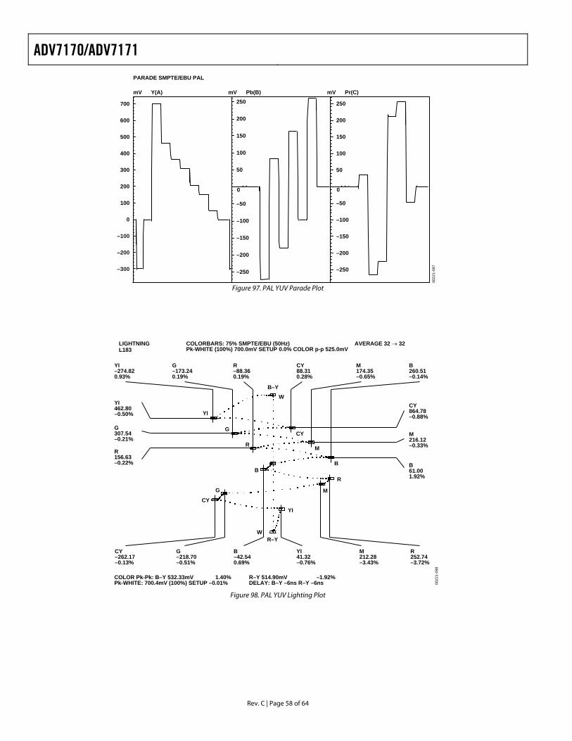
ADV7170/ADV7171
Rev. C | Page 58 of 64
PARADE SMPTE/EBU PAL
mV Y(A) mV Pb(B) mV Pr(C)
700
600
500
400
300
200
100
0
–100
–200
–300
250
200
150
100
50
–50
–100
–150
–200
–250
250
200
150
100
50
–50
–100
–150
–200
–250
0
0022
1-09
7
0
Figure 97. PAL YUV Parade Plot
LIGHTNING COLORBARS: 75% SMPTE/EBU (50Hz)Pk-WHITE (100%) 700.0mV SETUP 0.0% COLOR p-p 525.0mV
AVERAGE 32 → 32L183
YI–274.820.93%
G–173.240.19%
R–88.360.19%
CY88.310.28%
M174.35–0.65%
B260.51–0.14%
YI462.80–0.50%
G307.54–0.21%
R156.63–0.22%
B–YW
YI
G
R
B
G
CY
R–YW
YI
M
R
CY–262.17–0.13%
G–218.70–0.51%
B–42.540.69%
YI41.32–0.76%
M212.28–3.43%
R252.74–3.72%
CY864.78–0.88%
M216.12–0.33%
B61.001.92%
CY
M
B
COLOR Pk-Pk: B–Y 532.33mV 1.40%Pk-WHITE: 700.4mV (100%) SETUP –0.01%
R–Y 514.90mV –1.92%DELAY: B–Y –6ns R–Y –6ns 00
221-
098
Figure 98. PAL YUV Lighting Plot

ADV7170/ADV7171
Rev. C | Page 59 of 64
COMPONENT NOISELINE = 202AMPLITUDE (0dB = 700mV p-p)BANDWIDTH 10kHz TO 5.0MHz
NOISE dB RMS
–5.0
–10.0
–15.0
–20.0
–25.0
–30.0
–35.0
–40.0
–45.0
–50.0
–55.0
–60.0
–65.0
–70.0
–75.0
–80.0
–85.0
–90.0
–95.0
–100.01.0 2.0 3.0 4.0 5.0
(MHz)6.0
0.0
→Y 82.1Pb 82.3Pr 83.3
0022
1-09
9
Figure 99. PAL YUV SNR Plot
COMPONENT MULTIBURSTLINE = 202AMPLITUDE (0dB = 100% OF 688.1mV 683.4mV 668.9mV)
0.04 –0.02 –0.05 –0.68 –2.58 –8.05(dB)
0.49 0.99 2.00 3.99 4.79 5.79
0.49 0.99 1.99 2.39 2.89
0.49 0.99 1.99 2.39 2.89
0.0
–5.0
–10.0
Y
0.0
–5.0
–10.0
Pb
0.0
–5.0
–10.0
Pr
(MHz)
0.21 0.23 –0.78 –2.59 –7.15
0.25 0.25 –0.77 –2.59 –7.13
0022
1-10
0
Figure 100. PAL YUV Multiburst Response
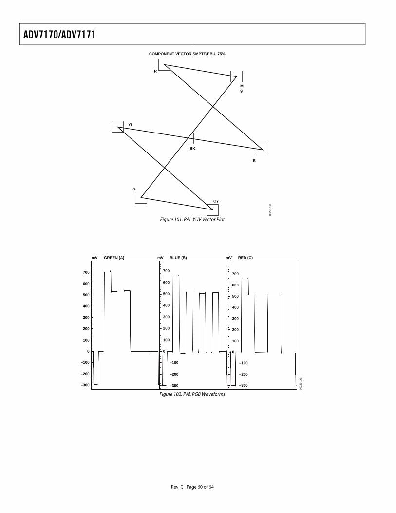
ADV7170/ADV7171
Rev. C | Page 60 of 64
R
Mg
YI
BK
B
G
CY
COMPONENT VECTOR SMPTE/EBU, 75%
0022
1-10
1
Figure 101. PAL YUV Vector Plot
mV GREEN (A) mV BLUE (B) mV RED (C)
700
600
500
400
300
200
100
0
–100
–200
–300
700
600
500
400
300
200
100
0
700
600
500
400
300
200
100
0
–100
–200
–300
–100
–200
–300
0022
1-10
2
Figure 102. PAL RGB Waveforms
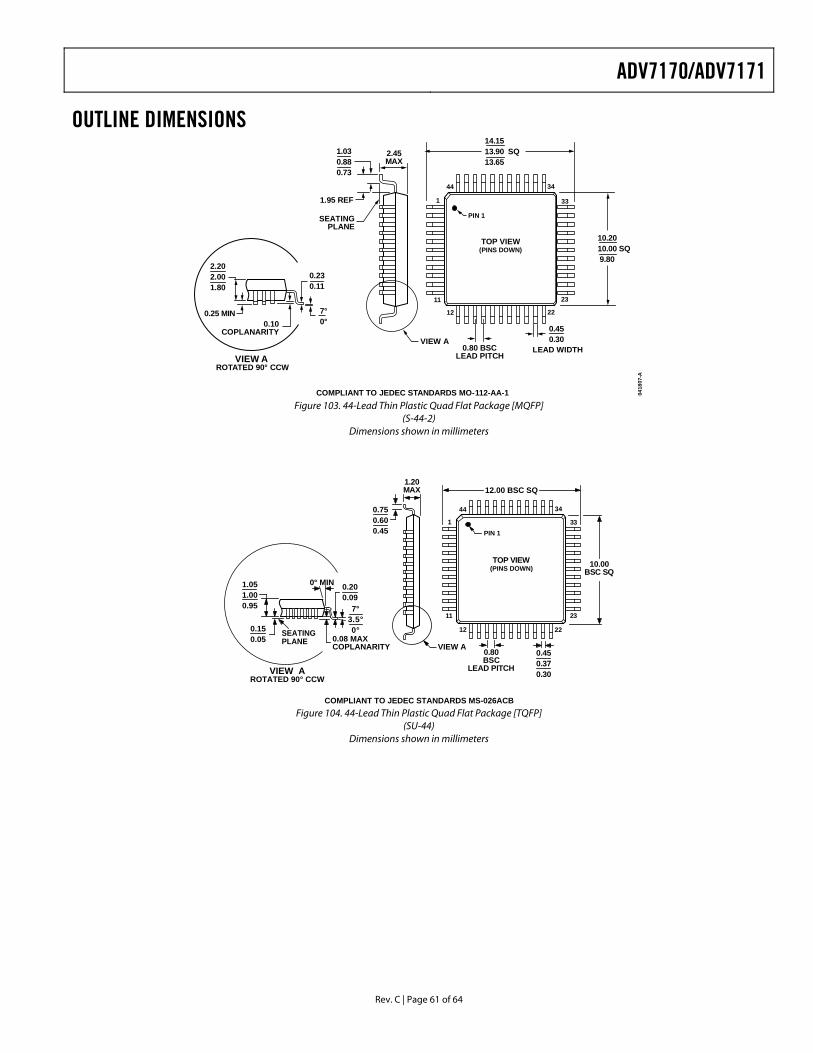
ADV7170/ADV7171
Rev. C | Page 61 of 64
OUTLINE DIMENSIONS
COMPLIANT TO JEDEC STANDARDS MO-112-AA-1 0418
07-A
14.1513.90 SQ13.65
0.450.30
2.45MAX
1.030.880.73
TOP VIEW(PINS DOWN)
12
44
1
22
23
34
33
11
0.25 MIN
2.202.001.80
7°0°
VIEW AROTATED 90° CCW
0.230.11
10.2010.00 SQ 9.80
0.80 BSCLEAD PITCH
LEAD WIDTH
0.10COPLANARITY
VIEW A
SEATINGPLANE
1.95 REF
PIN 1
Figure 103. 44-Lead Thin Plastic Quad Flat Package [MQFP]
(S-44-2) Dimensions shown in millimeters
COMPLIANT TO JEDEC STANDARDS MS-026ACB
1 33
3444
11
12
23
22
0.450.370.30
0.80BSC
LEAD PITCH
10.00BSC SQ
12.00 BSC SQ1.20MAX
0.750.600.45
1.051.000.95
0.200.09
0.08 MAXCOPLANARITY
SEATINGPLANE
0° MIN
7°3.5°0°0.15
0.05
VIEW AROTATED 90° CCW
VIEW A
PIN 1
TOP VIEW(PINS DOWN)
Figure 104. 44-Lead Thin Plastic Quad Flat Package [TQFP]
(SU-44) Dimensions shown in millimeters

ADV7170/ADV7171
Rev. C | Page 62 of 64
COMPLIANT TO JEDEC STANDARDS MS-022-AB-1 0418
07-A
13.4513.20 SQ12.95
0.450.29
2.45MAX
1.030.880.73
TOP VIEW(PINS DOWN)
12
44
1
22
23
34
33
110.250.10
2.202.001.80
7°0°
VIEW AROTATED 90° CCW
0.230.11
10.2010.00 SQ 9.80
0.80 BSCLEAD PITCH
LEAD WIDTH
0.10COPLANARITY
VIEW A
SEATINGPLANE
1.60 REF
PIN 1
Figure 105. 44-Lead Metric Quad Flat Package [MQFP]
(S-44-1) Dimensions shown in millimeters
ORDERING GUIDE Model Temperature Range Package Descriptions Package Options ADV7170KSZ1 −40°C to +85°C 44-Lead Metric Quad Flat Package [MQFP] S-44-2 ADV7170KSZ-REEL1
−40°C to +85°C 44-Lead Metric Quad Flat Package [MQFP] S-44-2 ADV7170KSUZ1
−40°C to +85°C 44-Lead Thin Plastic Quad Flat Package [TQFP] SU-44 ADV7170KSUZ-REEL1
−40°C to +85°C 44-Lead Thin Plastic Quad Flat Package [TQFP] SU-44 ADV7171KSZ1
−40°C to +85°C 44-Lead Metric Quad Flat Package [MQFP] S-44-2 ADV7171KSZ-REEL1
−40°C to +85°C 44-Lead Metric Quad Flat Package [MQFP] S-44-2 ADV7171KSUZ1
−40°C to +85°C 44-Lead Thin Plastic Quad Flat Package [TQFP] SU-44 ADV7171KSUZ-REEL1
−40°C to +85°C 44-Lead Thin Plastic Quad Flat Package [TQFP] SU-44 ADV7171WBSZ-REEL1
−40°C to +85°C 44-Lead Metric Quad Flat Package [MQFP] S-44-1 EVAL-ADV7170EBM Evaluation Board EVAL-ADV7171EBM Evaluation Board
1 Z = RoHS Compliant Part.

ADV7170/ADV7171
Rev. C | Page 63 of 64
NOTES

ADV7170/ADV7171
Rev. C | Page 64 of 64
NOTES
Purchase of licensed I2C components of Analog Devices or one of its sublicensed Associated Companies conveys a license for the purchaser under the Philips I2C Patent Rights to use these components in an I2C system, provided that the system conforms to the I2C Standard Specification as defined by Philips.
©2002–2009 Analog Devices, Inc. All rights reserved. Trademarks and registered trademarks are the property of their respective owners. Printed in the U.S.A. D00221-0-3/09(C)