ADSP-BF707 EZ-KIT Lite Evaluation System Manual ADSP-BF707 EZ-KIT Lite® Evaluation System Manual...
86
a ADSP-BF707 EZ-KIT Lite ® Evaluation System Manual Revision 1.0, May 2014 Part Number 82-000707-01 Analog Devices, Inc. One Technology Way Norwood, Mass. 02062-9106
Transcript of ADSP-BF707 EZ-KIT Lite Evaluation System Manual ADSP-BF707 EZ-KIT Lite® Evaluation System Manual...
a
ADSP-BF707 EZ-KIT Lite®
Evaluation System Manual
Revision 1.0, May 2014
Part Number82-000707-01
Analog Devices, Inc.One Technology WayNorwood, Mass. 02062-9106

Copyright Information©2014 Analog Devices, Inc., ALL RIGHTS RESERVED. This document may not be reproduced in any form without prior, express written consent from Analog Devices, Inc.
Printed in the USA.
DisclaimerAnalog Devices, Inc. reserves the right to change this product without prior notice. Information furnished by Analog Devices is believed to be accurate and reliable. However, no responsibility is assumed by Analog Devices for its use; nor for any infringement of patents or other rights of third parties which may result from its use. No license is granted by impli-cation or otherwise under the patent rights of Analog Devices, Inc.
Trademark and Service Mark NoticeThe Analog Devices logo, Blackfin, CrossCore, EngineerZone, EZ-Board, and EZ-KIT Lite are registered trademarks of Analog Devices, Inc.
Blackfin+ is a trademark of Analog Devices, Inc.
All other brand and product names are trademarks or service marks of their respective owners.

Regulatory Compliance The ADSP-BF707 EZ-KIT Lite is designed to be used solely in a labora-tory environment. The board is not intended for use as a consumer end product or as a portion of a consumer end product. The board is an open system design which does not include a shielded enclosure and therefore may cause interference to other electrical devices in close proximity. This board should not be used in or near any medical equipment or RF devices.
The ADSP-BF707 EZ-KIT Lite is in the process of being certified to com-ply with the essential requirements of the European EMC directive 2004/108/EC and therefore carries the “CE” mark.
The EZ-KIT Lite evaluation system contains ESD (electrostatic discharge) sensitive devices. Electrostatic charges readily accumulate on the human body and equipment and can discharge without detection. Permanent dam-age may occur on devices subjected to high-energy discharges. Proper ESD precautions are recommended to avoid performance degradation or loss of functionality. Store unused EZ-KIT Lite boards in the protective shipping package.


ADSP-BF707 EZ-KIT Lite Evaluation System Manual v
CONTENTS
PREFACE
Product Overview ............................................................................ x
Purpose of This Manual ................................................................ xiii
Intended Audience ........................................................................ xiii
Manual Contents ........................................................................... xiv
What’s New in This Manual ........................................................... xiv
Technical Support ........................................................................... xv
Supported Processors ....................................................................... xv
Supported Tools ............................................................................. xvi
Product Information ...................................................................... xvi
Analog Devices Web Site .......................................................... xvi
EngineerZone .......................................................................... xvii
Notation Conventions ................................................................... xvii

Contents
vi ADSP-BF707 EZ-KIT Lite Evaluation System Manual
USING ADSP-BF707 EZ-KIT LITE
Package Contents ......................................................................... 1-2
ADSP-BF707 EZ-Board ............................................................... 1-3
Default Configuration .................................................................. 1-3
EZ-KIT Lite Installation ............................................................... 1-5
EZ-KIT Lite Session Startup ......................................................... 1-6
Evaluation License ........................................................................ 1-8
DDR2 Memory ............................................................................ 1-8
SPI Flash ...................................................................................... 1-9
Housekeeping ADC .................................................................... 1-10
UART0 Interface ........................................................................ 1-10
CAN0 Interface .......................................................................... 1-10
CAN1 Interface .......................................................................... 1-11
USB Interface ............................................................................. 1-11
SD Interface ............................................................................... 1-12
Debug Interface .......................................................................... 1-12
Power-On-Self Test ..................................................................... 1-12
Expansion Interface .................................................................... 1-13
Power Architecture ..................................................................... 1-13
Power Measurements .................................................................. 1-14
Example Programs ...................................................................... 1-14
Reference Design Information ..................................................... 1-15

ADSP-BF707 EZ-KIT Lite Evaluation System Manual vii
Contents
ADSP-BF707 EZ-KIT LITE HARDWARE REFERENCE
System Architecture ...................................................................... 2-2
Software-Controlled Switches (SoftConfig) .................................... 2-3
Overview of SoftConfig ........................................................... 2-3
SoftConfig on the ADSP-BF707 EZ-KIT LITE ...................... 2-7
Programming SoftConfig Switches ........................................... 2-8
Push Buttons and Switches .......................................................... 2-16
Boot Mode Select Switch (SW1) ............................................ 2-17
Reset Push Button (SW2) ...................................................... 2-17
GPIO Push Buttons (SW3-4) ................................................ 2-17
Jumpers ...................................................................................... 2-18
Power Jumpers (P8-12, P14-18) ............................................. 2-18
LEDs .......................................................................................... 2-19
GPIO LEDs (LED3–5) ......................................................... 2-20
Reset LED (LED6) ................................................................ 2-20
Power LED (LED2) ............................................................... 2-20
SYS_FAULT LED (LED1) ..................................................... 2-20
Connectors ................................................................................. 2-21
Expansion Interface III Connectors (P1A-C) .......................... 2-22
Power Connector (P13) ......................................................... 2-22
USB to UART Connector (P6) .............................................. 2-22
USB Connector (P5) ............................................................. 2-23
RF Wireless Connector (J3) ................................................... 2-23
HADC SMC Connectors (J7, J8, J9) ..................................... 2-23

Contents
viii ADSP-BF707 EZ-KIT Lite Evaluation System Manual
HADC Connector (JP1) ....................................................... 2-24
SD Connector (J6) ................................................................ 2-24
CAN0 Connector (J4) ........................................................... 2-24
CAN1 Connector (J5) ........................................................... 2-25
JTAG/SWD/SWO Connector (P3) ....................................... 2-25
TRACE and JTAG/SWD/SWO Connector (P2) .................... 2-25
ADSP-BF707 EZ-KIT LITE BILL OF MATERIALS
ADSP-BF707 EZ-KIT LITE SCHEMATIC
INDEX

ADSP-BF707 EZ-KIT Lite Evaluation System Manual ix
PREFACE
Thank you for purchasing the ADSP-BF707 EZ-KIT Lite®, Analog Devices, Inc. low-cost evaluation system for the ADSP-BF70x Blackfin® processors.
The ADSP-BF707 processor is a member of the Blackfin family of prod-ucts. Blackfin processors combine a dual-MAC state-of-the-art signal processing engine, the advantages of a clean, orthogonal RISC-like micro-processor instruction set, and single-instruction, multiple-data (SIMD) multimedia capabilities into a single instruction-set architecture. New enhancements to the Blackfin+™ core add 32-bit MAC and 16-bit com-plex MAC support, cache enhancements, branch prediction and other instruction set improvements—all while maintaining instruction set com-patibility to previous Blackfin products.
The EZ-KIT Lite is shipped with all of the necessary hardware—you can start the evaluation immediately. The package contains the standalone evaluation board, CE-approved power supply, and USB cable. The EZ-KIT Lite version ships with an ICE-1000 emulator, while the EZ-Board® version is supported by the ICE-1000 or ICE-2000 emulator.
Expansion Interface III is provided for connecting a camera or audio extender board.
Traditional mechanical switches for changing the board’s factory setup have been removed in favor of I2C controlled software switches. The only remaining mechanical switches are the boot mode switch and push buttons.

Product Overview
x ADSP-BF707 EZ-KIT Lite Evaluation System Manual
The evaluation board is designed to be used in conjunction with the CrossCore® Embedded Studio (CCES) development tools to test capabil-ities of the ADSP-BF707 Blackfin processors. The CCES development environment aids advanced application code development and debug, such as:
• Create, compile, assemble, and link application programs written in C++, C, and assembly
• Load, run, step, halt, and set breakpoints in application programs
• Read and write data and program memory
• Read and write core and peripheral registers
Product OverviewThe board features:
• Analog Devices ADSP-BF707 processor
• 184-ball BGA package
• 25 MHz CLKIN core oscillator
• DDR2 memory (DMC0) chip
• 128M x 16-bit (2G bit)
• Micron MT47H128M16
• Quad SPI Flash (SPI2)
• 32M bit serial flash memory
• Winbond W25Q32

ADSP-BF707 EZ-KIT Lite Evaluation System Manual xi
Preface
• RF Wireless
• 4 x 2 connector
• 0.05” socket
• Universal Asynchronous Receiver/Transmitter (UART0)
• FTDI FT232RQ USB to UART converter
• USB Mini B connector
• Controller Area Network (CAN) interfaces
• CAN0—NXP TJA1041 transceiver and RJ11 connector
• CAN1—NXP TJA1041 transceiver and RJ11 connector
• USB0 interface
• Micro AB connector
• HADC
• VIN0 RTC battery through jumper
• VIN1 timer through RC
• VIN2 0.1” header
• VIN3 0.1” header
• RTC
• 16MM coin connector
• 3V 125 mAh Li-ion
• CR1632

Product Overview
xii ADSP-BF707 EZ-KIT Lite Evaluation System Manual
• RESET controller
• Analog Devices ADM6315 microprocessor supervisory circuits
• Debug (JTAG/SWD/TRACE) interface
• JTAG/SWD/SWO 10-pin 0.05” header for use with ADI emulators
• TRACE/JTAG/SWD 38-pin Mictor header
• Power measurement
• INA3221 to measure 3V, VDD_INT and VDD_EXT
• INA230 to measure VDD_DMC0
• LEDs
• Six LEDs: one power (green), one board reset (red), one SYS_FAULT (red), and three general-purpose (amber)
• Push buttons
• Three push buttons: one reset and two IRQ/Flag
• Expansion Interface III connectors (EI3)
• SMC0
• PPI
• SPORT
• SPI
• UART
• TWI
• TMR

ADSP-BF707 EZ-KIT Lite Evaluation System Manual xiii
Preface
• GPIOs
• PWR_IN
• GND/3.3V output
• External power supply
• CE compliant
• 5V @ 3.6 Amps
• Other features
• SD/MMC memory connector
• Boot mode switch
• 0.05-ohm resistors for processor current measurement
For information about the hardware components of the EZ-KIT Lite, refer to ADSP-BF707 EZ-KIT Lite Bill Of Materials.
Purpose of This ManualThe ADSP-BF707 EZ-KIT Lite Evaluation System Manual provides instructions for installing the product hardware (board). The text describes operation and configuration of the board components and pro-vides guidelines for running your own code on the ADSP-BF707 EZ-KIT Lite. Finally, a schematic and a bill of materials are provided for reference.
Intended AudienceThe primary audience for this manual is a programmer who is familiar with Analog Devices processors. This manual assumes that the audience has a working knowledge of the appropriate processor architecture, instruction set, and C/C++ programming languages.

Manual Contents
xiv ADSP-BF707 EZ-KIT Lite Evaluation System Manual
Programmers who are unfamiliar with Analog Devices processors can use this manual, but should supplement it with other texts (such as the ADSP-BF70x Blackfin+ Processor Hardware Reference and the ADSP-BF70x Blackfin+ Processor Programming Reference) that describe your target architecture.
Programmers who are unfamiliar with CrossCore Embedded Studio should refer to the CCES online help.
Manual ContentsThe manual consists of:
• Chapter 1, Using ADSP-BF707 EZ-KIT LiteDescribes EZ-KIT Lite functionality from a programmer’s perspec-tive and provides a simplified memory map of the processor.
• Chapter 2, ADSP-BF707 EZ-KIT Lite Hardware ReferenceProvides information about the EZ-KIT Lite hardware components.
• Appendix A, ADSP-BF707 EZ-KIT Lite Bill Of MaterialsProvides a list of hardware components used to manufacture the EZ-KIT Lite board.
• Appendix B, ADSP-BF707 EZ-KIT Lite SchematicLists the resources for board-level debugging.
What’s New in This ManualThis is the first revision (Revision 1.0) of the ADSP-BF707 EZ-KIT Lite Evaluation System Manual.

ADSP-BF707 EZ-KIT Lite Evaluation System Manual xv
Preface
Technical SupportYou can reach Analog Devices processors and DSP technical support in the following ways:
• Post your questions in the processors and DSP support community at EngineerZone®:http://ez.analog.com/community/dsp
• Submit your questions to technical support directly at:http://www.analog.com/support
• E-mail your questions about processors and processor applications to: [email protected] [email protected] (Greater China support)
• Contact your Analog Devices sales office or authorized distributor. Locate one at:www.analog.com/adi-sales
• Send questions by mail to:Processors and DSP Technical SupportAnalog Devices, Inc.Three Technology WayP.O. Box 9106Norwood, MA 02062-9106USA
Supported ProcessorsThis evaluation system supports Analog Devices ADSP-BF707 Blackfin processors.

Supported Tools
xvi ADSP-BF707 EZ-KIT Lite Evaluation System Manual
Supported ToolsInformation on supported tools for the ADSP-BF707 EZ-KIT Lite and the ADSP-BF70x family of Blackfin processors is available at:
http://www.analog.com/BF707EZKit
Product InformationProduct information can be obtained from the Analog Devices Web site and the online help system.
Analog Devices Web SiteThe Analog Devices Web site, www.analog.com, provides information about a broad range of products—analog integrated circuits, amplifiers, converters, and digital signal processors.
To access a complete technical library for each processor family, go to http://www.analog.com/processors/technical_library. The manuals selection opens a list of current manuals related to the product as well as a link to the previous revisions of the manuals. When locating your manual title, note a possible errata check mark next to the title that leads to the current correction report against the manual.
Also note, myAnalog.com is a free feature of the Analog Devices Web site that allows customization of a Web page to display only the latest information about products you are interested in. You can choose to receive weekly e-mail notifications containing updates to the Web pages that meet your interests, including documentation errata against all manu-als. myAnalog.com provides access to books, application notes, data sheets, code examples, and more.

ADSP-BF707 EZ-KIT Lite Evaluation System Manual xvii
Preface
Visit myAnalog.com (found on the Analog Devices home page) to sign up. If you are a registered user, just log on. Your user name is your e-mail address.
EngineerZoneEngineerZone is a technical support forum from Analog Devices. It allows you direct access to ADI technical support engineers. You can search FAQs and technical information to get quick answers to your embedded processing and DSP design questions.
Use EngineerZone to connect with other DSP developers who face similar design challenges. You can also use this open forum to share knowledge and collaborate with the ADI support team and your peers. Visit http://ez.analog.com to sign up.
Notation ConventionsText conventions used in this manual are identified and described as follows.
Example Description
File > Close Titles in reference sections indicate the location of an item within the CCES environment’s menu system (for example, the Close command appears on the File menu).
{this | that} Alternative required items in syntax descriptions appear within curly brackets and separated by vertical bars; read the example as this or that. One or the other is required.
[this | that] Optional items in syntax descriptions appear within brackets and sepa-rated by vertical bars; read the example as an optional this or that.
[this,…] Optional item lists in syntax descriptions appear within brackets delim-ited by commas and terminated with an ellipse; read the example as an optional comma-separated list of this.

Notation Conventions
xviii ADSP-BF707 EZ-KIT Lite Evaluation System Manual
.SECTION Commands, directives, keywords, and feature names are in text with letter gothic font.
filename Non-keyword placeholders appear in text with italic style format.
Note: For correct operation, ...A Note provides supplementary information on a related topic. In the online version of this book, the word Note appears instead of this
symbol.
Caution: Incorrect device operation may result if ...Caution: Device damage may result if ... A Caution identifies conditions or inappropriate usage of the product that could lead to undesirable results or product damage. In the online version of this book, the word Caution appears instead of this symbol.
Warning: Injury to device users may result if ... A Warning identifies conditions or inappropriate usage of the product that could lead to conditions that are potentially hazardous for the devices users. In the online version of this book, the word Warning appears instead of this symbol.
Example Description

ADSP-BF707 EZ-KIT Lite Evaluation System Manual 1-1
1 USING ADSP-BF707 EZ-KIT LITE
This chapter provides information to assist you with development of pro-grams for the ADSP-BF707 EZ-KIT Lite evaluation system.
The following topics are covered.
• Package Contents
• ADSP-BF707 EZ-Board
• Default Configuration
• EZ-KIT Lite Installation
• EZ-KIT Lite Session Startup
• Evaluation License
• DDR2 Memory
• SPI Flash
• Housekeeping ADC
• UART0 Interface
• CAN0 Interface
• CAN1 Interface
• USB Interface
• SD Interface

Package Contents
1-2 ADSP-BF707 EZ-KIT Lite Evaluation System Manual
• Debug Interface
• Power-On-Self Test
• Expansion Interface
• Power Architecture
• Power Measurements
• Example Programs
• Reference Design Information
Package ContentsYour ADSP-BF707 EZ-KIT Lite package contains the following items.
• ADSP-BF707 EZ-Board
• Universal 5V DC power
• USB A to micro B cable
• USB micro A to A receptacle cable
• ICE-1000 (only in the EZ-LIT Lite version)
• Standoffs and screws in a bag
• Release note
• 2GB SD card
Contact the vendor where you purchased your EZ-KIT Lite or contact Analog Devices, Inc. if any item is missing.

ADSP-BF707 EZ-KIT Lite Evaluation System Manual 1-3
Using ADSP-BF707 EZ-KIT Lite
ADSP-BF707 EZ-BoardThe ADSP-BF707 EZ-KIT Lite is shipped with an ICE-1000 emulator. When the product is not shipped with the emulator, it is referred to as the ADSP-BF707 EZ-Board.
The EZ-Board requires an ICE-1000 or ICE-2000 emulator.
Default ConfigurationThe ADSP-BF707 EZ-KIT Lite board is designed to run as a standalone unit.
When removing the EZ-KIT Lite board from the package, handle the board carefully to avoid the discharge of static electricity, which can dam-age some components.
The EZ-KIT Lite evaluation system contains ESD (electrostatic discharge) sensitive devices. Electrostatic charges readily accumulate on the human body and equipment and can discharge without detection. Permanent damage may occur on devices subjected to high-energy discharges. Proper ESD precau-tions are recommended to avoid performance degradation or loss of function-ality. Store unused EZ-KIT Lite boards in the protective shipping package.

Default Configuration
1-4 ADSP-BF707 EZ-KIT Lite Evaluation System Manual
Figure 1-1 shows the default jumper settings and boot mode switch used in installation. Confirm that your board is in the default configuration before using the board.
Figure 1-1. Default EZ-KIT Lite Hardware Setup

ADSP-BF707 EZ-KIT Lite Evaluation System Manual 1-5
Using ADSP-BF707 EZ-KIT Lite
EZ-KIT Lite InstallationIt is assumed that the CrossCore Embedded Studio software is installed and running on your PC.
Follow these instructions to ensure correct operation of the product soft-ware and hardware.
Step 1: Connecting an emulator to the EZ-KIT Lite.
1. Plug one side of the included USB cable into the USB connector of the emulator. Plug the other side into a USB port of the PC.
2. The status LED (labeled STATUS) should light up green if the con-nection with the PC is working and the appropriate Windows driver is installed. Please refer to the appropriate emulator manual if the status LED does not turn on.
3. Attach the emulator header (J2 on the bottom of the ICE-1000 to the P3 connector on the EZ-KIT Lite.
Step 2: Attach the provided cord and appropriate plug to the 5V power adaptor.
1. Plug the jack-end of the assembled power adaptor into the power connector P13 (labeled 5V) on the EZ-KIT Lite.
2. Plug the other side of the power adaptor into a power outlet. The power LED (labeled PWR) lights green when power is applied to the board.

EZ-KIT Lite Session Startup
1-6 ADSP-BF707 EZ-KIT Lite Evaluation System Manual
EZ-KIT Lite Session StartupIt is assumed that the CrossCore Embedded Studio software is installed and running on your PC.
Note: If you connect the board or emulator first (before installing CCES) to the PC, the Windows driver wizard may not find the board drivers.
1. Navigate to the CCES environment via the Start menu.
Note that CCES is not connected to the target board.
2. Use the Debug Configurations wizard to connect to the EZ-KIT Lite board.
If a debug configuration exists already, select the appropriate configuration and click Debug. Go to step 8.
To create a debug configuration, do one of the following:
• Click the down arrow next to the bug icon , select Debug Configurations
• Choose Run > Debug Configurations.
The Debug Configuration dialog box appears.
3. Select CrossCore Embedded Studio Application and click (New launch configuration).
The Select Processor page of the Session Wizard appears.
4. Ensure Blackfin is selected in Processor family. In Processor type, select ADSP-BF707. Click Next.
The Select Connection Type page of the Session Wizard appears.

ADSP-BF707 EZ-KIT Lite Evaluation System Manual 1-7
Using ADSP-BF707 EZ-KIT Lite
5. Select Emulator and click Next.
The Select Platform page of the Session Wizard appears.
6. Choose the type of emulator that is connected to the EZ-KIT Lite.
7. Click Finish to close the wizard.
The new debug configuration is created and added to the Debug Configurations list.
8. In the Name edit box, users can select an appropriate name to describe the configuration, otherwise a default name is provided.
9. In the Program(s) to load section, choose the program to load (if the appropriate program is not already populated) when connect-ing to the board. If not loading any program upon connection to the target, do not make any changes.
While connected to the target, there is no way to choose a program to download. To load a program once connected, terminate the session and then load the new program.
To delete a configuration, go to the Debug Configurations dialog box and select the configuration to delete. Click and choose Yes when asked if you wish to delete the selected launch configuration. Then Close the dialog box.
To disconnect from the target board, click the terminate button or choose Run > Terminate.
To delete a session, choose Target > Session > Session List. Select the session name from the list and click Delete. Click OK.
The default configurations that show up in the CCES Debug Con-figurations wizard are for JTAG mode debugging only. To use SWD mode, a new platform will need to be created using the Tar-get Configurator.

Evaluation License
1-8 ADSP-BF707 EZ-KIT Lite Evaluation System Manual
Evaluation LicenseWhen starting CCES for the first time, you will be prompted to install either a 90-day evaluation license or a permanent, full license. To auto-matically install an unrestricted 90-day evaluation license, select “I do not have a serial number and would like to evaluate the product”. If the evalu-ation license is installed but not activated, it allows 10 days of unrestricted use and then becomes disabled. The license can be re-enabled by activa-tion. Once activated, the evaluation license offers 90 days of unrestricted use and then becomes permanently disabled.
An evaluation license can be upgraded to a full license. Licenses can be purchased from:
• Analog Devices directly. Call (800) 262-5645 or 781-937-2384 or go to: http://www.analog.com/buyonline.
• Analog Devices, Inc. local sales office or authorized distributor. To locate one, go to:www.analog.com/adi-sales.
The EZ-KIT Lite hardware must be connected and powered up to use CCES with a valid evaluation or full license.
DDR2 MemoryThe ADSP-BF707 processor connects to a 2Gb Micron MT47H128M16 chip through the Double Data Rate Synchronous Dynamic Ran-dom-Access Memory (DDR2 SDRAM) controller. The DDR2 memory controller on the processor and the DDR2 memory chip are powered by the on-board 1.8V regulator. Data is transferred between the processor and DDR2 on both the rising and falling edges of the DDR2 clock. The DDR2 controller on the processor can operate at a maximum clock fre-quency of 200 MHz.

ADSP-BF707 EZ-KIT Lite Evaluation System Manual 1-9
Using ADSP-BF707 EZ-KIT Lite
With a CCES session running and connected to the EZ-KIT Lite via an emulator, the DDR2 registers are configured automatically each time the processor is reset through a soft reset using CCES. The values are used whenever DDR2 is accessed through the debugger (for example, when viewing memory or loading a program).
To disable the automatic setting of the DDR2 registers, select Target Options from the Session menu in CCES and uncheck Use XML reset values.
An example program is included in the EZ-KIT Lite installation directory to demonstrate how to set up and access the DDR2 interface. For more information on how to initialize the registers after a reset, refer to the hardware reference manual.
SPI FlashThe ADSP-BF707 processor has three SPI interfaces: SPI0, SPI1, and SPI2. SPI2 is connected to a Winbond W25Q32BC 32 Mb serial flash memory with dual and quad SPI support. This flash is used for booting and scratchpad space.
Quad mode is enabled by default. The processor flag signals, PB_15 (SPI2_SEL1), PB_13 (SPI2_D2), and PB_14 (SPI2_D3) are connected by default and can be disconnected by using SoftConfig. Refer to Soft-ware-Controlled Switches (SoftConfig) for more information.
For more information, refer to the SPI flash example in the POST, which is included in the ADSP-BF707 Board Support Package.

Housekeeping ADC
1-10 ADSP-BF707 EZ-KIT Lite Evaluation System Manual
Housekeeping ADCThe ADSP-BF707 processor provides four housekeeping ADC inputs: HADC0_VIN0 through HADC_VIN3. The EZ-KIT Lite connects HADC0_VIN0 to pin 2 of a four position 0.1” header (JP1). JP1 has VDD_RTC voltage domain on pin 1, allowing a jumper to connect the voltage back to the processor. Pin 4 of JP1 connects through an RC timer to HADC0_VIN1.
HADC_VIN2 and HADC_VIN3 are connected to SMC connectors (J7 and J8). Refer to ADSP-BF707 EZ-KIT Lite Schematic for more information.
UART0 InterfaceThe ADSP-BF707 processor has two built-in universal asynchronous transmitters (UARTs). UART0 is connected to an FTDI, FT232RQ, USB to UART converter IC (U45).
The UART functionality is connected by default through SoftConfig. Refer to Software-Controlled Switches (SoftConfig) for more information.
For more information, refer to the UART0 example in the POST, which is included in the ADSP-BF707 Board Support Package.
CAN0 InterfaceThe Controller Area Network 0 (CAN0) interface of the EZ-KIT Lite is connected to the NXP TJA1041 CAN transceiver (U46). The transceiver is attached to the CAN0 port of the ADSP-BF707processor via an RJ-11 con-nector (J4). See CAN0 Connector (J4).
The CAN0 transmit, receive, and error signals are connected through the SoftConfig switches and disabled by default. CAN0_EN is enabled by default and CAN0_STB is disabled. See Software-Controlled Switches (SoftConfig).
ADSP-BF707 EZ-KIT Lite Evaluation System Manual 1-11
Using ADSP-BF707 EZ-KIT Lite
For more information, refer to the CAN0 example in the POST, which is included in the ADSP-BF707 Board Support Package.
CAN1 InterfaceThe Controller Area Network 1 (CAN1) interface of the EZ-KIT Lite is connected to the NXP TJA1041 CAN transceiver (U47). The transceiver is attached to the CAN1 port of the ADSP-BF707 processor via an RJ-11 con-nector (J5). See CAN1 Connector (J5).
The CAN1 transmit and receive signals are connected through the SoftCon-fig switches and enabled by default. CAN1_EN is enabled by default. CAN1_ERR_EN (error) and CAN1_STB are disabled. See Software-Controlled Switches (SoftConfig).
For more information, refer to the CAN1 example in the POST, which is included in the ADSP-BF707 Board Support Package.
USB InterfaceThe ADSP-BF707 processor has an integrated USB PHY; the EZ-KIT Lite provides a micro AB connector. The board supports USB high speed mode.
The board supplies a maximum of 5V at 500 mA to a peripheral device by enabling the FET switch (U40). The USB controller controls the FET switch through the USB0_VBC signal.
To learn about the processor’s device and host modes, refer to the USB example in the POST, which is included in the ADSP-BF707 Board Sup-port Package. For more information, refer to the hardware reference manual.

SD Interface
1-12 ADSP-BF707 EZ-KIT Lite Evaluation System Manual
SD InterfaceThe ADSP-BF707 processor has a secure digital (SD) interface that con-sists of a clock pin, command pin, card detect pin, and an 8-bit data bus. SoftConfig controls the connection of the card detect pin (PA_08) and a GPIO pin used for write protect (PB_07). Refer to Software-Controlled Switches (SoftConfig) and SD Connector (J6) for more details.
An example program is included in the ADSP-BF707 Board Support Package.
Debug InterfaceThe EZ-KIT Lite provides a JTAG/SWD/SWO connection via connector (P3), which is a 0.05” pitch header. An 8-bit trace connection also is avail-able via connector (P2), although this is not supported at this time. See JTAG/SWD/SWO Connector (P3) and TRACE and JTAG/SWD/SWO Connector (P2) for more information.
Power-On-Self TestThe Power-On-Self-Test Program (POST) tests all EZ-KIT Lite peripher-als and validates functionality as well as connectivity to the processor. Once assembled, each EZ-KIT Lite is fully tested for an extended period of time with POST. All EZ-KIT Lite boards are shipped with POST pre-loaded into flash memory. The POST is executed by resetting the board and pressing the proper push button(s). The POST also can be used as a reference for a custom software design or hardware troubleshooting.
Note that the source code for the POST program is included in the ADSP-BF707 Board Support Package along with the readme.txt file that describes how the board is configured to run POST.

ADSP-BF707 EZ-KIT Lite Evaluation System Manual 1-13
Using ADSP-BF707 EZ-KIT Lite
Expansion InterfaceThe expansion interface allows a custom-design daughter board to be tested across various hardware platforms that have the same expansion interface.
The Expansion Interface III (EI3) implemented on the ADSP-BF707 EZ-KIT Lite consists of three connectors: P1A, P1B, and P1C. The con-nectors contain a majority of the processor’s signals. For pinout information, go to ADSP-BF707 EZ-KIT Lite Schematic.
Limits to current and interface speed must be taken into consideration when using the expansion interface. Current for extenders connected to the EI3 connectors can be sourced from the EZ-KIT Lite; therefore, the current should be limited to 250 mA for 5V, and 300 mA from the 3.3V planes. If more current is required, a separate power connector and a regu-lator must be designed on the daughter card. Additional circuitry implemented on extender cards can add extra loading to signals, decreas-ing their maximum effective speed.
Analog Devices does not support and is not responsible for the effects of additional circuitry.
Power ArchitectureThe ADSP-BF707 EZ-KIT Lite has three primary voltage domains: 3.3V, 1.1V, and 1.8V. The power input is a 5V wall adaptor.
The Analog Devices ADP5024 controller provides all three voltage levels, 3.3V for the VDD_EXT signal and the 3.3V power requirements of the board, the VDD_INT signal (1.1V), as well as the VDD_DMC0 signal (1.8V).
The voltage levels can be measured using INA3221 IC (U48) for 3.3V, VDD_INT, and VDD_EXT. Current consumption of the power rail could be measured with this same device when the corresponding jumper is

Power Measurements
1-14 ADSP-BF707 EZ-KIT Lite Evaluation System Manual
removed. See Power Measurements for more information. The voltage level of VDD_DMC0 can be measured by using the INA230 IC (U31) and the current consumption of the domain, if the jumper is removed. See Power Measurements section for more information
A FET switch (U40) controls the 5V to the USB devices over the USB0_VBUS signal.
Power MeasurementsLocations are provided for measuring the current draw from various power planes. Precision 0.05 ohm shunt resistors are available on the VDD_EXT, VDD_INT, USB0_VBUS, and 3.3V and voltage domains. For current draw, the jumper is removed, voltage across the resistor can be measured using an oscilloscope, and the value of the resistor can be measured using a preci-sion multi-meter. Once voltage and resistance are measured, the current can be calculated by dividing the voltage by the resistance. For the highest accuracy, a differential probe should be used for measuring the voltage across the resistor.
There are also ICs (U48 and U31) that can be used to measure the current consumption of each power rail in software when the jumper is removed. For more information, refer to Power Jumpers (P8-12, P14-18).
Example ProgramsExample programs are provided with the ADSP-BF707 Board Support Package to demonstrate various capabilities of the product. The programs can be found in the ADSP-BF707_EZ-Board-Rel1.0.0\examples folder. The number after the “Rel” could be higher for newer versions. Refer to a readme file provided with each example for more information.

ADSP-BF707 EZ-KIT Lite Evaluation System Manual 1-15
Using ADSP-BF707 EZ-KIT Lite
Reference Design InformationA reference design info package is available for download on the Analog Devices Web site. The package provides information on the design, lay-out, fabrication, and assembly of the EZ-KIT Lite.
The information can be found at:
http://www.analog.com/BF707EZKit

Reference Design Information
1-16 ADSP-BF707 EZ-KIT Lite Evaluation System Manual

ADSP-BF707 EZ-KIT Lite Evaluation System Manual 2-1
2 ADSP-BF707 EZ-KIT LITE HARDWARE REFERENCE
This chapter describes the hardware design of the ADSP-BF707 EZ-KIT Lite board.
The following topics are covered.
• System ArchitectureDescribes the board’s configuration and explains how the board components interface with the processor.
• Software-Controlled Switches (SoftConfig)Lists and describes the processor signals routed through the soft-ware-controlled switches.
• Push Buttons and SwitchesShows the locations and describes the push buttons and switches.
• JumpersShows the locations and describes the configuration jumpers.
• LEDsShows the locations and describes the LEDs.
• ConnectorsShows the locations and provides part numbers for the on-board connectors. In addition, the manufacturer and part number infor-mation is provided for the mating parts.

System Architecture
2-2 ADSP-BF707 EZ-KIT Lite Evaluation System Manual
System ArchitectureThis section describes the processor’s configuration on the EZ-KIT Lite board (Figure 2-1).
This EZ-KIT Lite is designed to demonstrate the ADSP-BF707 proces-sor’s capabilities. The ADSP-BF707 EZ-KIT Lite has a 25 MHz input clock and runs at 400 MHz internally.
USB circuitry and a micro USB AB connector are provided for connecting to the EZ-KIT Lite as a host or a device. The frequency for the USB cir-cuit is generated by an external 24 MHz oscillator.
Figure 2-1. EZ-KIT Lite Block Diagram
ADSP-BF707BGA 400MHz LEDs (3)
Deb
ug
Port
SPI225 MHz Oscillator
PBs (2)
CLK
IN
GPI
O
UART0 USB0
USB otg
CAN0
CANRJ11
JTAG/SWD/SWO 10 pin 0.05"
CAN1
CANRJ11
NXPTJA1041
NXPTJA1041
EI3 (1A , 1B, 1C)
TRACE 38 pin mictor
DMC0
32 Mbit Quad SPI Flash
2GB DDR2 SD/MMC
Conn
MSI0
RF WirelessSPI2
RTC
16mm battery holder
ADP50245V1.8V1.1V3.3V
FTDIFT232RQ
USB
24 MHz Oscillator
32.768 kHz Oscillator

ADSP-BF707 EZ-KIT Lite Evaluation System Manual 2-3
ADSP-BF707 EZ-KIT Lite Hardware Reference
User I/O to the processor is provided in the form of two user push buttons and three LEDs. The software-controlled switches (SoftConfig) facilitate the switch multi-functionality by disconnecting the push buttons from their associated processor pins and reusing the pins elsewhere on the board. See ADSP-BF707 EZ-KIT Lite Schematic for more information.
Software-Controlled Switches (SoftConfig)
On the ADSP-BF707 EZ-KIT Lite, most of the traditional mechanical switches have been replaced by I2C software-controlled switches. The remaining mechanical switches are provided for the boot mode and push buttons. Reference any SoftConfig*.c file found in the installation direc-tory for an example of how to set up the SoftConfig feature of the ADSP-BF707 EZ-KIT Lite through software.
The SoftConfig section of this manual serves as a reference to any user that intends to modify an existing software example. If software provided from ADI is used, there should be little need to reference this section.
Care should be taken when changing SoftConfig settings not to create a conflict with interfaces. This is especially true when con-necting extender cards.
Overview of SoftConfigIn order to further clarify the use of electronic single FET switches and multi-channel bus switches, an example of each is illustrated and com-pared to a traditional mechanical switching solution. This is a generic example that uses the same FET and bus switch components that are on the EZ-KIT Lite.
After this generic discussion there is a detailed explanation of the Soft-Config interface specific to the ADSP-BF707 EZ-KIT Lite.

Software-Controlled Switches (SoftConfig)
2-4 ADSP-BF707 EZ-KIT Lite Evaluation System Manual
Figure 2-2 shows two individual FET switches (Pericom PI3A125CEX) with reference designators UA and UB. Net names ENABLE_A and ENABLE_B control UA and UB. The default FET switch enable settings in this exam-ple are controlled by resistors RA and RB which pull the enable pin 1 of UA and UB to ground (low). In a real example, these enable signals are con-trolled by the Microchip IO expander. The default pull-down resistors connects the signals EXAMPLE_SIGNAL_A and EXAMPLE_SIGNAL_B and also connects signals EXAMPLE_SIGNAL_C and EXAMPLE_SIGNAL_D. To disconnect EXAMPLE_SIGNAL_A from EXAMPLE_SIGNAL_B, the Microchip IO expander is used to change ENABLE_A to a logic 1 through software that interfaces with the Microchip. The same procedure for ENABLE_B would disconnect EXAM-PLE_SIGNAL_C from EXAMPLE_SIGNAL_D.
Figure 2-2. Example of Individual FET Switches

ADSP-BF707 EZ-KIT Lite Evaluation System Manual 2-5
ADSP-BF707 EZ-KIT Lite Hardware Reference
Figure 2-3 shows the equivalent circuit to Figure 2-2 but utilizes mechan-ical switches that are in the same package. Notice the default is shown by black boxes located closer to the ON label of the switches. In order to dis-connect these switches, physically move the switch to the OFF position.
Figure 2-4 shows a bus switch example, reference designator UC (Pericom PI3LVD512ZHE), selecting between lettered functionality and numbered functionality. The signals on the left side are multiplexed signals with naming convention letter_number. The right side of the circuit shows the signals separated into letter and number, with the number on the lower group (eg. 0B1) and the letter on the upper group (eg. 0B2). The default setting is controlled by the signal CONTROL_LETTER_NUMBER which is pulled low. This selects the number signals on the right to be connected to the multiplexed signals on the left by default. In this example, the Microchip IO expander is not shown but controls the signal CONTROL_LETTER_NUMBER and allows the user to change the selection through software.
Figure 2-5 shows the equivalent circuit to Figure 2-4 but utilizes mechan-ical switches. Notice the default for reference designators SWC and SWD is illustrated by black boxes located closer to the ON label of the switches to enable the number signals by default. Also notice the default setting for reference designators SWE and SWF is OFF. In order to connect the letters instead of the numbers, the user physically changes all switches on SWC and SWD to the OFF position and all switches on SWE and SEF to the ON position.
Figure 2-3. Example of Mechanical Switch Equivalent to Figure 2-2

Software-Controlled Switches (SoftConfig)
2-6 ADSP-BF707 EZ-KIT Lite Evaluation System Manual
Figure 2-4. Example of Bus Switch

ADSP-BF707 EZ-KIT Lite Evaluation System Manual 2-7
ADSP-BF707 EZ-KIT Lite Hardware Reference
SoftConfig on the ADSP-BF707 EZ-KIT LITETwo Microchip MCP23017 GPIO expanders provide control for individ-ual electronic switches. The TWI0 interface of the processor communicates with the Microchip devices.There are individual switches with default settings that enable basic board functionality.
Table 2-1 lists the ADSP-BF707 processor and EZ-KIT Lite interfaces that are available by default. Note that only interfaces affected by software switches are listed in Table 2-1.
Figure 2-5. Example of Mechanical Switch Equivalent to Figure 2-4

Software-Controlled Switches (SoftConfig)
2-8 ADSP-BF707 EZ-KIT Lite Evaluation System Manual
Programming SoftConfig SwitchesOn the ADSP-BF707 EZ-KIT Lite, two Microchip MCP23017 devices exist. Each of these devices have the following programming characteristics:
• Each switch has two programmable GPIO registers.
• Each GPIO register controls eight signals (software switches).
• By default, the Microchip MCP23017 GPIO signals function as input signals.
The signals must be programmed as output signals to override their default values. The following tables (Table 2-2 and Table 2-3) show the Microchip register addresses and the values that must be written to them to program the signals as output signals.
Table 2-1. Default ADSP-BF707 Processor Interface Availability
Interface Availability by Default
UART0 USB to UART conversion through U45 (FTDI FT232RQ) with flow control
CAN0 Transmit/receive disabled
CAN1 Enabled
Push buttons Enabled
LEDs Enabled
GPIO Register Register Address
GPIOA 0x12
GPIOB 0x13

ADSP-BF707 EZ-KIT Lite Evaluation System Manual 2-9
ADSP-BF707 EZ-KIT Lite Hardware Reference
Each of the examples in the ADSP-BF707 Board Support Package include source files that program the soft switches, even if the default settings are being used. The README for each example identifies only the signals that are being changed from their default values. The code that programs the soft switches is located in the SoftConfig_BF707.c file, with a version number suffix, in each example.
The following tables (Table 2-4 and Table 2-5) outline the default values for each of the two Microchip MCP23017 devices.
Table 2-2. IODIR for Hardware Address 0x41
IODIR Register IODIR Register Address Value to be Written to Program Signals as Outputs
IODIRA 0x00 0x40
IODIRB 0x01 0x03
Table 2-3. IODIR for Hardware Address 0x42
IODIR Register IODIR Register Address Value to be Written to Program Signals as Outputs
IODIRA 0x00 0x80
IODIRB 0x01 0x83
Table 2-4. I2C Hardware Address 0x41
GPIO MCP23017 Register Address Default Value
GPIOA 0x12 0xF8
GPIOB 0x13 0xFF

Software-Controlled Switches (SoftConfig)
2-10 ADSP-BF707 EZ-KIT Lite Evaluation System Manual
The ADSP-BF707 EZ-KIT Lite Schematic shows how the two Microchip GPIO expanders are connected to the board’s ICs.
Table 2-6 and Table 2-7 show the output signals of the Microchip GPIO expander (U39), with a TWI address of 0100 001X, where X represents the read or write bit. The signals that control an individual FET have an entry under the FET column. The Component Connected column shows the board IC that is connected if the FET is enabled. The Microchip (U39) is controlling the enable signal of a FET switch. Also note that if a particular functionality of the processor signal is being used, it will be in bold font under the Processor Signal column.
Table 2-5. I2C Hardware Address 0x42
GPIO MCP23017 Register Address Default Value
GPIOA 0x12 0x85
GPIOB 0x13 0x83
Table 2-6. Output Signals of Microchip GPIO Expander (U39 Port A)
Bit Signal Name Description FET Processor Signal (if applicable)
Component Connected
Default
0 SPIFLASH_CS_EN SPI flash CS U3 PB_15/SPI2_SEL1/TRACE0_D00/SMC0_D15/SPI2_SS
U33 Low
1 SPIFLASH_D2_EN SPI flash D2 U4 PB_13/SPI2_D2/UART1_RTS/TRACE0_D02/SMC0_D13
U33 Low
2 SPIFLASH_D3_EN SPI flash D3 U5 PB_14/SPI2_D3/UART1_CTS/TRACE0_D01/SMC0_D14
U33 Low
3 RF_SPI2_SEL1_EN RF wireless SPI chip select
U28 PB_15/SPI2_SEL1/TRACE0_D00/SMC0_D15/SPI2_SS
J3 High

ADSP-BF707 EZ-KIT Lite Evaluation System Manual 2-11
ADSP-BF707 EZ-KIT Lite Hardware Reference
4 SD_CD_EN MSIO card detect U26 PA_08/EPPI0_D11/MSI0_CD/SPT1_ACLK/SMC0_A01
J6 High
5 SD_WP_EN GPIO SD card write protect
U27 PB_07/EPPI0_D00/SPT0_BD1/SPI0_D3/SMC0_D00/SYS_WAKE0
J6 High
6 Not Used
7 RF_SPI2_SEL2_EN RF wireless SPI chip select
U29 PB_08/UART0_TX/EP-PI0_D16/SPI2_SEL2/SMC0_D08/SYS_WAKE1
J3 High
Table 2-7. Output Signals of Microchip GPIO Expander (U39 Port B)
Bit Signal Name Description FET Processor Signal (if applicable)
Component Connected
Default
0 Not Used
1 Not Used
2 CAN0_EN Enables CAN0 U46 High
3 CAN0_STB Puts CAN IC in standby U46 High
4 CAN1_EN Enables CAN1 U47 High
5 CAN1_STB Puts CAN IC in standby U47 High
Table 2-6. Output Signals of Microchip GPIO Expander (U39 Port A) (Cont’d)
Bit Signal Name Description FET Processor Signal (if applicable)
Component Connected
Default

Software-Controlled Switches (SoftConfig)
2-12 ADSP-BF707 EZ-KIT Lite Evaluation System Manual
Table 2-8 and Table 2-9 show the output signals of the Microchip GPIO expander (U38), with a TWI address of 0100 010X, where X represents the read or write bit. The signals that control an individual FET have an entry under the FET column. The Component Connected column shows the board IC that is connected if the FET is enabled. Note that some of the Microchip (U38) output signals are connected directly to components on the board. However, in most cases, the Microchip (U38) is controlling the enable signal of a FET switch. Also note that if a particular functionality of the processor signal is being used, it will be in bold font under the Pro-cessor Signal column.
6 CAN0_ERR_EN Connects CAN error sig-nal to processor
U6 PB_02/EPPI0_D05/SPT1_BD0/SPI0_MOSI/SMC0_D05
U46 High
7 CAN1_ERR_EN Connects CAN error sig-nal to processor
U9 PB_03/EPPI0_D04/SPT1_BD1/SPI0_D2/SMC0_D04
U47 High
Table 2-7. Output Signals of Microchip GPIO Expander (U39 Port B) (Cont’d)
Bit Signal Name Description FET Processor Signal (if applicable)
Component Connected
Default

ADSP-BF707 EZ-KIT Lite Evaluation System Manual 2-13
ADSP-BF707 EZ-KIT Lite Hardware Reference
Table 2-8. Output Signals of Microchip GPIO Expander (U38 Port A)
Bit Signal Name Description FET/SWITCH
Processor Signal (if applicable)
Component Connected
Default
0 CAN0_TX_EN Enables CAN0 TX U10 PC_03/UART0_CTS/CAN0_TX/EPPI0_D12/SMC0_A11/TM0_ACI0
U46 High
1 CAN1_TX_EN Enables CAN1 TX U7 PA_13/EPPI0_FS2/CAN1_TX/SMC0_ARE/CNT0_ZM
U47 Low
2 CAN0_RX_EN Enables CAN0 RX U11 PC_02/UART0_RTS/CAN0_RX/EPPI0_D13/SMC0_A10/TM0_ACI5/SYS_WAKE3
U46 High
3 CAN1_RX_EN Enables CAN1 RX U8 PA_12/EPPI0_FS1/CAN1_RX/SMC0_AOE/TM0_ACI6/SYS_WAKE4
U47 Low
4 UART0_EN Enables UART0 U12/U13 PB_09/UART0_RX/EPPI0_D17/SPI2_SEL3/SMC0_D09/TM0_ACI3 and PB_08/UART0_TX/EPPI0_D16/SPI2_SEL2/SMC0_D08/SYS_WAKE1
U45 Low
5 UART0RTS_EN Enables UART0 RTS U51 PC_02/UART0_RTS/CAN0_RX/EPPI0_D13/SMC0_A10/TM0_ACI5/SYS_WAKE3
U45 Low

Software-Controlled Switches (SoftConfig)
2-14 ADSP-BF707 EZ-KIT Lite Evaluation System Manual
6 UART0CTS_EN Enables UART0 CTS U50 PC_03/UART0_CTS/CAN0_TX/EPPI0_D12/SMC0_A11/TM0_ACI0
U45 Low
7 Not Used
Table 2-9. Output Signals of Microchip GPIO Expander (U38 Port B)
Bit Signal Name Description FET/SWITCH
Processor Signal (if applicable)
Component Connected
Default
0 Not Used
1 Not Used
2 LED1_GPIO1_EN Enables LED1 U23 PA_00/SPI1_CLK/TRACE0_D07/SMC0_ABE0
U2 Low
3 LED2_GPIO2_EN Enables LED2 U24 PA_01/SPI1_MISO/TRACE0_D06/SMC0_ABE1
U2 Low
4 LED3_GPIO3_EN Enables LED3 U25 PB_01/EPPI0_D06/SPT1_BFS/SPI0_MI-SO/SMC0_D06/TM0_ACI1
U2 Low
5 PUSHBUTTON1_EN Enables push button 1 U21 PA_02/SPI1_MOSI/TRACE0_D05/SMC0_AMS1
SW4 Low
Table 2-8. Output Signals of Microchip GPIO Expander (U38 Port A) (Cont’d)
Bit Signal Name Description FET/SWITCH
Processor Signal (if applicable)
Component Connected
Default
ADSP-BF707 EZ-KIT Lite Evaluation System Manual 2-15
ADSP-BF707 EZ-KIT Lite Hardware Reference
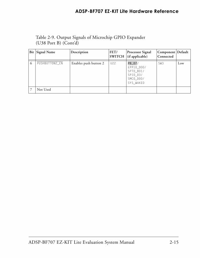
6 PUSHBUTTON2_EN Enables push button 2 U22 PB_07/EPPI0_D00/SPT0_BD1/SPI0_D3/SMC0_D00/SYS_WAKE0
SW3 Low
7 Not Used
Table 2-9. Output Signals of Microchip GPIO Expander (U38 Port B) (Cont’d)
Bit Signal Name Description FET/SWITCH
Processor Signal (if applicable)
Component Connected
Default
Push Buttons and Switches
2-16 ADSP-BF707 EZ-KIT Lite Evaluation System Manual
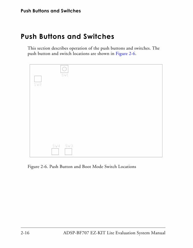
Push Buttons and SwitchesThis section describes operation of the push buttons and switches. The push button and switch locations are shown in Figure 2-6.
Figure 2-6. Push Button and Boot Mode Switch Locations

ADSP-BF707 EZ-KIT Lite Evaluation System Manual 2-17
ADSP-BF707 EZ-KIT Lite Hardware Reference
Boot Mode Select Switch (SW1)The rotary switch (SW1) determines the boot mode of the processor. Table 2-10 shows the available boot mode settings. By default, the ADSP-BF707 processor boots from the internal SPI flash memory.
Reset Push Button (SW2)The reset push button (SW2) resets the following ICs: processor (U1), GPIO extender (U39), and GPIO extender (U38). The reset also is con-nected to the expansion interface via the SYS_HWRST signal.
GPIO Push Buttons (SW3-4)The GPIO push buttons (SW3 and SW4) are connected to the processor’s signals PA_02/SPI1_MOSI/TRACE0_D05/SMC0_AMS1 and PB_07/EPPI0_D00/SPT0_BD1/SPI0_D3/SMC0_D00/SYS_WAKE0, respectively. The signals are con-nected by default. A monostable pulse generator (one-shot, U49) on push button 2 shortens the wake pulse, allowing the processor to return to low power mode sooner.
Table 2-10. Boot Mode Select Switch (SW1)
SW1 Position Processor Boot Mode
0 No Boot – Idle
1 SPI master boot (SP12). Default boot mode.
2 SPI slave boot (SPI2)
3 UART boot (UART0)
Jumpers
2-18 ADSP-BF707 EZ-KIT Lite Evaluation System Manual
JumpersThis section describes functionality of the configuration jumpers. Figure 2-7 shows the jumper locations.
Power Jumpers (P8-12, P14-18)Remove jumpers listed in Table 2-11 to measure the respective voltage across the adjacent sense resistor.
Figure 2-7. Jumper Locations
Table 2-11. Power Jumpers
Power Jumper Resistor
P8 VDD_INT
P9 3.3V
P10 VDD_EXT
P11 USB0_VBUS

ADSP-BF707 EZ-KIT Lite Evaluation System Manual 2-19
ADSP-BF707 EZ-KIT Lite Hardware Reference
LEDsThis section describes the on-board LEDs. Figure 2-8 shows the LED locations.
P12 VDD_DMC0
P14 VDD_HADC
P15 VDD_OTP
P16 VDD_USB
P17 VDD_RTC
P18 HADC_VREFP (no sense resistor, remove to supply HADC_VREFP through J9)
Figure 2-8. LED Locations
Table 2-11. Power Jumpers (Cont’d)
Power Jumper Resistor

LEDs
2-20 ADSP-BF707 EZ-KIT Lite Evaluation System Manual
GPIO LEDs (LED3–5)Three LEDs are connected to the general-purpose I/O pins of the proces-sor (see Table 2-12). The LEDs are active high and are ON (amber) by writing a 1 to the correct processor signal.
Reset LED (LED6)When LED6 is ON (red), it indicates that the master reset of all the major ICs is active. The reset LED is controlled by the Analog Devices ADM6315 supervisory reset circuit. TARGET_RESET is a signal driven from an emulator. EI3 extender cards can also drive a reset as an input to this reset circuit. A master reset is asserted by pressing SW2 which activates LED6. For more information, see Reset Push Button (SW2).
Power LED (LED2)When LED2 is ON (green), it indicates that power is being supplied to the board properly. For more information, see Power Architecture.
SYS_FAULT LED (LED1)When SYS_FAULT LED (LED1) (red) is ON, it indicates a system fault. For more information, refer to the hardware reference manual.
Table 2-12. GPIO LEDs
LED Reference Designator Processor Programmable Flag Pin
LED3 PA_00
LED4 PA_01
LED5 PB_01

ADSP-BF707 EZ-KIT Lite Evaluation System Manual 2-21
ADSP-BF707 EZ-KIT Lite Hardware Reference
ConnectorsThis section describes connector functionality and provides information about mating connectors. The connector locations are shown in Figure 2-9.
Connectors on the back of the board are noted with dotted lines.
Figure 2-9. Connector Locations

Connectors
2-22 ADSP-BF707 EZ-KIT Lite Evaluation System Manual
Expansion Interface III Connectors (P1A-C)Three board-to-board connectors (P1A, P1B, P1C) provide signals from the SPI, TWI, UART, SPORT, and GPIO interfaces of the processor. The connectors are located on the bottom side of the board.
For more information, see Expansion Interface.
Power Connector (P13)
USB to UART Connector (P6)
Part Description Manufacturer Part Number
120-pin, 0.6 mm Hirose FX8-120P-SV1(91)
Mating Cable
120-pin, 0.6 mm Hirose FX8-120S-SV(21)
Part Description Manufacturer Part Number
0.65 mm power jack CUI 045-0883R
Mating Cable
[email protected] power supply GLOBETEK GS-1750(R)
Part Description Manufacturer Part Number
USB Mini-B Hirose UX60SC-MB-5S8
Mating Cable
USB Mini-B to Standard-A cable Any

ADSP-BF707 EZ-KIT Lite Evaluation System Manual 2-23
ADSP-BF707 EZ-KIT Lite Hardware Reference
USB Connector (P5)
RF Wireless Connector (J3)
HADC SMC Connectors (J7, J8, J9)J7 allows an input to the HADC_VIN2 signal of the processor. J8 allows an input to the HADC_VIN3 signal of the processor. J9 allows the HADC_VREFP signal to be injected if the P18 jumper is removed.
Part Description Manufacturer Part Number
USB Micro-AB Hirose ZX62D-AB-5P8
Mating Cable
USB Micro-B to Standard-A or Micro-A to Standard-A receptacle cable
Any
Part Description Manufacturer Part Number
4x2 0.05” pitch socket SAMTEC SFMC-104-T2-S-D
Mating Connector
4x2 0.05” pitch header SAMTEC FTSH-104-04-F-D
Part Description Manufacturer Part Number
SMC threaded Amphenol 152119
Mating Cable
SMC cable Various

Connectors
2-24 ADSP-BF707 EZ-KIT Lite Evaluation System Manual
HADC Connector (JP1)JP1 allows the VDD_RTC signal to be connected to HADC0_VIN0 with the installation of a jumper across pins 1 and 2. Pin 3 is not connected. Pin 4 allows the user to probe HADC0_VIN1 which is connected to an RC timer driven by TM0_TMR3 on PC_05.
SD Connector (J6)
CAN0 Connector (J4)
Part Description Manufacturer Part Number
2x2 0.1” header SAMTEC TSM-102-01-T-DV
Mating Devices
Jumper for pins 1 and 2, probe for pin 4
Part Description Manufacturer Part Number
SD 8-bit, 2 GB SANDISK MHC-W21-601
Mating Card
2 GB SANDISK SDSDB-2048-A11
Part Description Manufacturer Part Number
RJ11 vertical DIGIKEY A31431-ND
Mating Cable
RJ11 cable
ADSP-BF707 EZ-KIT Lite Evaluation System Manual 2-25
ADSP-BF707 EZ-KIT Lite Hardware Reference
CAN1 Connector (J5)
JTAG/SWD/SWO Connector (P3)The JTAG/SWD/SWO header (P3) provides debug connectivity for the processor. This is a 0.05” shrouded through-hole connector from SAM-TEC (SHF-105-01-L-D-TH). This mates with ICE-1000, ICE-2000, and any newer ADI emulators. For more information, see Debug Interface.
TRACE and JTAG/SWD/SWO Connector (P2)The TRACE and JTAG/SWD/SWO Connector (P2) provides connectiv-ity to the microprocessor’s trace interface. This is a MICTOR connector from TYCO (2-5767004-2). There are no trace pods available at this time. If one does become available, R162, R191, R192, and R193 need to be installed to connect P2.
Part Description Manufacturer Part Number
RJ11 vertical DIGIKEY A31431-ND
Mating Cable
RJ11 cable

Connectors
2-26 ADSP-BF707 EZ-KIT Lite Evaluation System Manual

ADSP-BF707 EZ-KIT Lite Evaluation System Manual A-1
A ADSP-BF707 EZ-KIT LITE BILL OF MATERIALS
The bill of materials corresponds to ADSP-BF707 EZ-KIT Lite Schematic.
Ref. Qty. DescriptionReference Designator Manufacturer Part Number
1 3 SMC THREADED AMPHE-NOL_152119
J7-J9 AMPHENOL CONN
152119
2 1 ADP5024 QFN50P400X400-25N
VR1 ADI ADP5024ACPZ-R2
3 1 ADM6315 SOT143 U37 ADI ADM6315-29D2ARTZR7
4 1 ADSP-BF707 BGA184C80P14X14_1200X1200_SCKT
U1 ADI ADSP-BF707BBCZ-ENG
5 1 10UF 6.3V 10% 0805 X5R
C124 AVX 08056D106KAT2A
6 43 0.1UF 10V 10% 0402 X5R
C1,C2,C5,C20-C22,C25,C26,C28-C32,C38,C40-C42,C47,C49,C50,C54,C66-C68,C74-C76,C78-C81,C95,C96,C125-C128,C142-C144,C146,C148,C152
AVX 0402ZD104KAT2A

A-2 ADSP-BF707 EZ-KIT Lite Evaluation System Manual
7 56 0.01UF 16V 10% 0402 X7R
C3,C6-C19,C23,C33-C37,C43-C46,C51-C53,C56-C58,C60,C61,C65,C69,C73,C77,C97-C99,C102-C104,C106-C111,C123,C129,C139-C141,C147,C150
AVX 0402YC103KAT2A
8 3 4.7UF 25V 20% 0805 X5R
C24,C121,C122 AVX 0805ZD475KAT2A
9 1 4.7UF 6.3V 20% 0603 C145 AVX 06036D475MAT2A
10 4 100PF 50V 5% 0603 NPO
C62,C63,C70,C71 AVX 06035A101JAT2A
11 1 27PF 50V 5% 0402 NPO
C134 AVX 04025A270JAT2A
12 1 10UF 16V 10% 1210 X5R
C113 AVX 1210YD106KAT2A
13 2 1000PF 50V 5% 1206 C112,C114 AVX 12065A102JAT2A
14 1 ROTARY SWT027 SW1 COPAL S-8110
15 2 1UF 16V 10% 0603 X5R
C82,C120 DIGI-KEY 399-5090-2-ND
16 2 MCP23017 QFN65P600X600-29N
U38,U39 DIGI-KEY MCP23017-E/ML-ND
17 1 USB 5PIN CON069 P6 DIGI-KEY H11589CT-ND
18 2 1UF 16V 10% 0805 X7R
C115,C116 DIGI-KEY 399-1284-2-ND
19 1 GREEN LED_0603 LED2 DIGI-KEY 475-1409-2-ND
20 2 4700PF 2A FIL_N-FE61PT
FER7,FER8 DIGI-KEY 490-2554-2-ND
21 1 25MHZ OSC-CC200X250
U36 DIGI-KEY 478-4780-1-ND
Ref. Qty. DescriptionReference Designator Manufacturer Part Number

ADSP-BF707 EZ-KIT Lite Evaluation System Manual A-3
ADSP-BF707 EZ-KIT Lite Bill Of Materials
22 1 FT232RQ QFN50P500X500-33NA
U45 DIGI-KEY 768-1008-1-ND
23 1 24MHZ OSC-CC200X250
U35 DIGI-KEY 478-4778-1-ND
24 1 USB-MICRO 5PIN HIROSE_ZX-62D-AB-5P8
P5 DIGI-KEY H11494CT-ND
25 1 30A GSOT05 SOT23-3
D2 DIGI-KEY GSOT05-E3-08TR-ND
26 2 RED LED_0603 LED1,LED6 DIGI-KEY 475-2512-2-ND
27 3 YELLOW LED_0603 LED3-LED5 DIGI-KEY 475-2558-1-ND
28 2 15KV ESDA5V3SC6 SOT95P280-6N
D3,D4 DIGI-KEY 497-6633-1-ND
29 1 MIC2025-1 SOIC8 U40 DIGI-KEY 576-1057-ND
30 1 32.768KHZ OSC_ABS07L
Y3 DIGI-KEY 535-9542-2-ND
31 1 INA3221 QFN65P400X400-17N
U48 DIGI-KEY 296-30459-1-ND
32 1 INA230 QFN50P300X300-17N
U31 DIGI-KEY 296-30346-2-ND
33 5 IDC 2PIN_-JUMPER_SHORT
SJ1-SJ5 DIGI-KEY S9001-ND
34 1 PWR .65MM CON045
P13 DIGI-KEY CP1-023-ND
35 1 150UF 10V 10% D TANT-LOW-ESR
CT1 DIGI-KEY 478-3321-2-ND
36 2 4700PF 16V 10% 0603 X7R
C64,C72 DIGI-KEY 311-1083-2-ND
Ref. Qty. DescriptionReference Designator Manufacturer Part Number

A-4 ADSP-BF707 EZ-KIT Lite Evaluation System Manual
37 1 750.0K 1/10W 1% 0603
R179 DIGI-KEY 311-750KHRTR-ND
38 2 100 1/16W 5% 0402 R73,R74 DIGI-KEY 311-100JRTR-ND
39 1 12.0K 1/16W 1% 0402
R116 DIGI-KEY 311-12.0KLRCT-ND
40 6 330.0 1/16W 1% 0402
R4,R62,R80-R83 DIGI-KEY 541-330LCT-ND
41 2 10.0K 1/16W 1% 0402
R113,R118 DIGI-KEY 541-10.0KLCT-ND
42 8 100K 1/16W 5% 0402 R180-R187 DIGI-KEY 541-100KJTR-ND
43 2 15PF 50V 5% 0402 NPO
C132,C133 DIGI-KEY 399-1014-2-ND
44 1 100.0 1/16W 1% 0402
R21 DIGI-KEY 541-100LCT-ND
45 1 15.0K 1/16W 1% 0402 ZZZ
R119 DIGI-KEY 311-15.0KLRTR-ND
46 1 56.0K 1/16W 1% 0402
R101 DIGI-KEY 311-56.0KLRTR-ND
47 1 1UH 30% IND_LQH32P
L1 DIGI-KEY 490-5334-1-ND
48 1 1UH 30% INDC2016 L2 DIGI-KEY 490-7784-2-ND
49 1 20MA MA3X717E DIO005
D1 DIODES INC BAS70-05-7-F
50 10 IDC 2X1 IDC2X1 P8-P12,P14-P18 FCI 90726-402HLF
51 3 0.6MM 120PIN HIROSE_FX8-120P-SV1(91)
P1A,P1B,P1C HIROSE FX8-120P-SV1(91)
52 1 IDT74FCT3244APY SSOP20
U2 IDT IDT74FCT3244APYG
53 1 TEST LOOP LOOP_2838
GP1 KEYSTONE 5016
Ref. Qty. DescriptionReference Designator Manufacturer Part Number

ADSP-BF707 EZ-KIT Lite Evaluation System Manual A-5
ADSP-BF707 EZ-KIT Lite Bill Of Materials
54 1 LTC6993-1 SOT95P280-6N
U49 LINEAR TECHNOLOGY
LTC6993CS6-1#TRMPBF
55 1 VARISTOR V5.5MLA 30A 0603
R1 LITTLEFUSE V5.5MLA0603
56 1 PTC 0.5A 1206 R161 LITTLEFUSE 1206L050-C
57 1 BATT_HOLDER 16MM BATT_-COIN16MM
J1 MEMORY PROTECTIONDEVICES
BH600
58 1 MT47H128M16 FBGA84
U32 MICRON MT47H128M16RT-25E XIT:C
59 1 SD_CONN 8-BIT CON067
J6 MORETHANALL MHC-W21-601-LF
60 10 10UF 6.3V 20% 0603 X5R
C4,C27,C39,C48,C55,C59,C117-C119,C149
MULTICOMP MCCA000517
61 1 190 5A FER002 FER6 MURATA DLW5BSN191SQ2
62 2 1UF 6.3V 20% 0402 X5R
C100,C101 MURATA GRM155R60J105ME19D
63 2 TJA1041 SOIC14 U46,U47 NXP TJA1041T/CM,118
64 1 5A MBRS540T3G SMC
D7 ON SEMI MBRS540T3G
65 2 15KV ESD7004 DFN50P250X100-10N
D5,D6 ON SEMI ESD7004MUTAG
66 3 MOMENTARY SWT024
SW2-SW4 PANASONIC EVQ-Q2K03W
67 13 0 1/10W 5% 0402 R24,R102,R104,R115,R135,R136,R145,R146,R162,R176,R191-R193
PANASONIC ERJ-2GE0R00X
68 16 0 1/10W 5% 0402 R2,R3,R10,R13,R15,R25,R61,R111,R114,R131,R132,R140,R175,R177,R188,R189
PANASONIC ERJ-2GE0R00X
Ref. Qty. DescriptionReference Designator Manufacturer Part Number

A-6 ADSP-BF707 EZ-KIT Lite Evaluation System Manual
69 4 0.1 1/10W 1% 0603 R169-R172 PANASONIC ERJ-3RSFR10V
70 2 1.0K 1/16W 1% 0402 R19,R20 PANASONIC ERJ-2RKF1001X
71 1 33 1/16W 5% RNS003
RN1 PANASONIC EXB-2HV330JV
72 2 2.2K 1/10W 5% 0402 R8,R9 PANASONIC ERJ-2GEJ222X
73 4 60.4 1/10W 1% 0603 R26,R32,R34,R40 PANASONIC ERJ-3EKF60R4V
74 1 39.0K 1/10W 1% 0402 ZZZ
R117 PANASONIC ERJ-2RKF3902X
75 1 0.0 1/10W 1% 0603 R190 PHYCOMP 232270296001L
76 1 IDC 2x2 IDC2X2_SMT
JP1 SAMTEC TSM-102-01-T-DV
77 1 IDC 4x2 SAMTEC_S-FMC-104-T2-S-D
J3 SAMTEC SFMC-104-T2-S-D
78 1 0.05 10PIN SAM-TEC_SHF-105-01-L-D-TH
P3 SAMTEC SHF-105-01-L-D-TH-TR
79 5 0.051 1/2W 1% 1206 R92,R105,R106,R112,R120
SEI CSF 1/2 0.05 1%R
80 5 600 500MA 1206 FER1-FER5 STEWARD HZ1206B601R-10
81 1 74LVC14A SOIC14 U30 TI 74LVC14AD
82 2 SN74LVC1G08 SOT23-5
U42,U44 TI SN74LVC1G08DBVE
83 22 PI3A125 SC70_5 U3-U13,U21-U29,U50,U51
TI SN74CBTLV1G125DCKR
84 1 MICTOR 38PIN CON015
P2 TYCO 2-5767004-2
85 2 RJ11 4PIN CON039 J4,J5 TYCO 5558872-1
86 1 3A RESETABLE FUS004
F1 TYCO SMD300F-2
87 1 0 1/8W 5% 0805 R22 VISHAY CRCW08050000Z0EA
Ref. Qty. DescriptionReference Designator Manufacturer Part Number

ADSP-BF707 EZ-KIT Lite Evaluation System Manual A-7
ADSP-BF707 EZ-KIT Lite Bill Of Materials
88 18 10K 1/16W 5% 0402 R12,R28,R36,R44,R93,R94,R97,R107-R109,R151,R153,R154,R156,R158,R159,R168,R178
VISHAY CRCW040210K0FKED
89 80 10K 1/16W 5% 0402 R5-R7,R11,R14,R16-R18,R29,R31,R33,R37,R39,R41-R43,R45-R52,R63-R65,R67,R70-R72,R77-R79,R84-R91,R95,R96,R98-R100,R103,R110,R122-R129,R134,R137-R139,R142-R144,R148-R150,R152,R155,R157,R160,R163-R167,R173,R174,R196,R197
VISHAY CRCW040210K0FKED
90 6 33 1/16W 5% 0402 R68,R75,R121,R130,R133,R147
VISHAY CRCW040233R0JNEA
91 1 10M 1/10W 5% 0603 R195 VISHAY CRCW060310M0FNEA
92 2 1M 1/10W 5% 0603 R23,R194 VISHAY CRCW06031M00FNEA
93 4 10 1/10W 5% 0603 R27,R30,R35,R38 VISHAY CRCW060310R0JNEA
94 1 W25Q32 SO8W U33 WINBOND W25Q32FVSSIG
Ref. Qty. DescriptionReference Designator Manufacturer Part Number

A-8 ADSP-BF707 EZ-KIT Lite Evaluation System Manual

D
4
3
2
1
A B C
20 Cotton Road
Nashua, NH 03063
A B C D
4
3
2
1
PH: 1-800-ANALOGD
C
Title
Size Board No.
Date Sheet of
DEVICESANALOG
Rev1.013
A0450-2013
ADSP-BF707 EZ-BOARD
04/04/2014
Title
1
ADSP-BF707 EZ-BoardSCHEMATIC

D
4
3
2
1
A B C
20 Cotton Road
Nashua, NH 03063
A B C D
4
3
2
1
PH: 1-800-ANALOGD
C
Title
Size Board No.
Date Sheet of
DEVICESANALOG
Rev1.013
A0450-2013
ADSP-BF707 EZ-BOARD
04/04/2014
Proc Ports, JTAG, Trace
2
JTG_TCK/SWCLK
JTG_TDI
JTG_TDO/SWO
JTG_TMS/SWDIO
JTG_TRST
USB0_CLKIN
USB0_DM
USB0_DP
USB0_ID
USB0_VBC
USB0_VBUS
USB0_XTAL
SYS_XTAL
HADC0_VIN0
HADC0_VIN1
HADC0_VIN2
HADC0_VIN3
TWI0_SCL
TWI0_SDA
RTC0_CLKIN
RTC0_XTAL
SYS_CLKIN
SYS_CLKOUT
SYS_BMODE0
SYS_BMODE1
SYS_EXTWAKE
SYS_FAULT
SYS_HWRST
SYS_NMI
SYS_RESOUT
U1
ADSP-BF707
J3
C7
C13
F12
C5
C14
E12
H3
M14
N1
M2
L2
L3
P11
N11
N12
P12
N14
P5
M6
M7
N6
N7
P7
P6
D3
C2
C1
E3
C3
P2
CON015
38373635
33 3432313028
2927
262422201816
252321191715
1113
9
1357
42
6
108
1214
PA_00/SPI1_CLK/TRACE0_D07/SMC0_ABE0
PA_01/SPI1_MISO/TRACE0_D06/SMC0_ABE1
PA_02/SPI1_MOSI/TRACE0_D05/SMC0_AMS1
PA_03/SPI1_SEL2/SPI1_RDY/SMC0_ARDY
PA_04/SPI1_SEL1/TM0_TMR7/SPI2_RDY/SMC0_A08/SPI1_SS
PA_05/TM0_TMR0/SPI0_SEL1/SMC0_A07/SPI0_SS
PA_06/TM0_TMR1/SPI0_SEL2/SPI0_RDY/SMC0_A06
PA_07/TM0_TMR2/SPT1_BTDV/SPT1_ATDV/SMC0_A05/CNT0_DG
PB_08/UART0_TX/EPPI0_D16/SPI2_SEL2/SMC0_D08/SYS_WAKE1
PB_09/UART0_RX/EPPI0_D17/SPI2_SEL3/SMC0_D09/TM0_ACI3
PB_10/SPI2_CLK/TRACE0_CLK/SMC0_D10/TM0_ACLK4
PB_11/SPI2_MISO/TRACE0_D04/SMC0_D11
PB_12/SPI2_MOSI/TRACE0_D03/SMC0_D12/SYS_WAKE2
PB_13/SPI2_D2/UART1_RTS/TRACE0_D02/SMC0_D13
PB_14/SPI2_D3/UART1_CTS/TRACE0_D01/SMC0_D14
PB_15/SPI2_SEL1/TRACE0_D00/SMC0_D15/SPI2_SS
PA_08/EPPI0_D11/MSI0_CD/SPT1_ACLK/SMC0_A01
PA_09/EPPI0_D10/TM0_TMR4/SPT1_AFS/SMC0_A02
PA_10/EPPI0_D09/TM0_TMR5/SPT1_AD0/SMC0_A03
PA_11/EPPI0_D08/TM0_TMR6/SPT1_AD1/SMC0_A04
PA_12/EPPI0_FS1/CAN1_RX/SMC0_AOE/TM0_ACI6/SYS_WAKE4
PA_13/EPPI0_FS2/CAN1_TX/SMC0_ARE/CNT0_ZM
PA_14/EPPI0_CLK/SPI1_SEL4/SMC0_AWE/TM0_ACLK5
PA_15/EPPI0_FS3/SPT0_ATDV/SPT0_BTDV/SMC0_AMS0/CNT0_UD
PB_00/EPPI0_D07/SPT1_BCLK/SPI0_CLK/SMC0_D07/TM0_ACLK3
PB_01/EPPI0_D06/SPT1_BFS/SPI0_MISO/SMC0_D06/TM0_ACI1
PB_02/EPPI0_D05/SPT1_BD0/SPI0_MOSI/SMC0_D05
PB_03/EPPI0_D04/SPT1_BD1/SPI0_D2/SMC0_D04
PB_04/EPPI0_D03/SPT0_BCLK/SPI0_SEL4/SMC0_D03/TM0_ACLK6
PB_05/EPPI0_D02/SPT0_BD0/SPI0_SEL5/SMC0_D02
PB_06/EPPI0_D01/SPT0_BFS/SPI0_SEL6/SMC0_D01/TM0_CLK
PB_07/EPPI0_D00/SPT0_BD1/SPI0_D3/SMC0_D00/SYS_WAKE0
PC_00/UART1_TX/SPT0_AD1/EPPI0_D15
PC_01/UART1_RX/SPT0_BD1/EPPI0_D14/SMC0_A09/TM0_ACI4
PC_02/UART0_RTS/CAN0_RX/EPPI0_D13/SMC0_A10/TM0_ACI5/SYS_WAKE3
PC_03/UART0_CTS/CAN0_TX/EPPI0_D12/SMC0_A11/TM0_ACI0
PC_04/SPT0_BCLK/SPI0_CLK/MSI0_D1/SMC0_A12/TM0_ACLK0
PC_05/SPT0_AFS/TM0_TMR3/MSI0_CMD
PC_06/SPT0_BD0/SPI0_MISO/MSI0_D3
PC_07/SPT0_BFS/SPI0_MOSI/MSI0_D2/TM0_ACI2
PC_08/SPT0_AD0/SPI0_D2/MSI0_D0
PC_09/SPT0_ACLK/SPI0_D3/MSI0_CLK/TM0_ACLK2
PC_10/SPT1_BCLK/MSI0_D4/SPI1_SEL3/TM0_ACLK1
PC_11/SPT1_BFS/MSI0_D5/SPI0_SEL3
PC_12/SPT1_BD0/MSI0_D6
PC_13/SPT1_BD1/MSI0_D7
PC_14/SPT1_BTDV/MSI0_INT
U1
ADSP-BF707
N4
P4
M5
N5
H2
F3
G3
H1
J2
J1
K1
L1
K3
K2
M1
P8
N9
M9
M10
M12
L12
M11
N10
N13
P13
J12
K12
H13
H12
G12
D12
M3
N2
P2
M4
N3
P3
M8
N8
C12
C11
C10
C9
A9
C6
C4
G2
R2 00402
R3 00402
3.3V
04020R162
04020R191
04020R192
3.3V
330.00402
R4
TP1 TP2
040210KR5
040210KR6
TP33.3V 3.3V
10K0402
R7
3.3V
LED_0603REDLED1
04020R193
TP4TP9
R82.2K0402
R92.2K0402
3.3V
R10 00402
3.3V
R1110K0402
DNP
R1210K0402
04020R13
040210KR163
SYS_HWRST
PC_02/UART0_RTS/CAN0_RX/EPPI0_D13/SMC0_A10/TM0_ACI5/SYS_WAKE3
PC_03/UART0_CTS/CAN0_TX/EPPI0_D12/SMC0_A11/TM0_ACI0
PA_12/EPPI0_FS1/CAN1_RX/SMC0_AOE/TM0_ACI6/SYS_WAKE4
PA_13/EPPI0_FS2/CAN1_TX/SMC0_ARE/CNT0_ZM
PB_15/SPI2_SEL1/TRACE0_D00/SMC0_D15/SPI2_SS
PB_15/SPI2_SEL1/TRACE0_D00/SMC0_D15/SPI2_SS
PB_14/SPI2_D3/UART1_CTS/TRACE0_D01/SMC0_D14
PB_14/SPI2_D3/UART1_CTS/TRACE0_D01/SMC0_D14
PB_13/SPI2_D2/UART1_RTS/TRACE0_D02/SMC0_D13
PB_13/SPI2_D2/UART1_RTS/TRACE0_D02/SMC0_D13
PB_12/SPI2_MOSI/TRACE0_D03/SMC0_D12/SYS_WAKE2
PB_12/SPI2_MOSI/TRACE0_D03/SMC0_D12/SYS_WAKE2
PB_11/SPI2_MISO/TRACE0_D04/SMC0_D11
PB_11/SPI2_MISO/TRACE0_D04/SMC0_D11
PB_10/SPI2_CLK/TRACE0_CLK/SMC0_D10/TM0_ACLK4
PB_10/SPI2_CLK/TRACE0_CLK/SMC0_D10/TM0_ACLK4
SYS_EXTWAKE
PC_00/UART1_TX/SPT0_AD1/EPPI0_D15
PC_01/UART1_RX/SPT0_BD1/EPPI0_D14/SMC0_A09/TM0_ACI4
PC_04/SPT0_BCLK/SPI0_CLK/MSI0_D1/SMC0_A12/TM0_ACLK0
PC_05/SPT0_AFS/TM0_TMR3/MSI0_CMD
PC_06/SPT0_BD0/SPI0_MISO/MSI0_D3
PC_07/SPT0_BFS/SPI0_MOSI/MSI0_D2/TM0_ACI2
PC_08/SPT0_AD0/SPI0_D2/MSI0_D0
PC_09/SPT0_ACLK/SPI0_D3/MSI0_CLK/TM0_ACLK2
PC_10/SPT1_BCLK/MSI0_D4/SPI1_SEL3/TM0_ACLK1
PC_11/SPT1_BFS/MSI0_D5/SPI0_SEL3
PC_12/SPT1_BD0/MSI0_D6
PC_13/SPT1_BD1/MSI0_D7
PC_14/SPT1_BTDV/MSI0_INT
PA_00/SPI1_CLK/TRACE0_D07/SMC0_ABE0
PA_00/SPI1_CLK/TRACE0_D07/SMC0_ABE0
PA_01/SPI1_MISO/TRACE0_D06/SMC0_ABE1
PA_01/SPI1_MISO/TRACE0_D06/SMC0_ABE1
PA_02/SPI1_MOSI/TRACE0_D05/SMC0_AMS1
PA_02/SPI1_MOSI/TRACE0_D05/SMC0_AMS1
PA_03/SPI1_SEL2/SPI1_RDY/SMC0_ARDY
PA_04/SPI1_SEL1/TM0_TMR7/SPI2_RDY/SMC0_A08/SPI1_SS
PA_05/TM0_TMR0/SPI0_SEL1/SMC0_A07/SPI0_SS
PA_06/TM0_TMR1/SPI0_SEL2/SPI0_RDY/SMC0_A06
PA_07/TM0_TMR2/SPT1_BTDV/SPT1_ATDV/SMC0_A05/CNT0_DG
PA_08/EPPI0_D11/MSI0_CD/SPT1_ACLK/SMC0_A01
PA_09/EPPI0_D10/TM0_TMR4/SPT1_AFS/SMC0_A02
PA_10/EPPI0_D09/TM0_TMR5/SPT1_AD0/SMC0_A03
PA_11/EPPI0_D08/TM0_TMR6/SPT1_AD1/SMC0_A04
PA_14/EPPI0_CLK/SPI1_SEL4/SMC0_AWE/TM0_ACLK5
PA_15/EPPI0_FS3/SPT0_ATDV/SPT0_BTDV/SMC0_AMS0/CNT0_UD
PB_00/EPPI0_D07/SPT1_BCLK/SPI0_CLK/SMC0_D07/TM0_ACLK3
PB_01/EPPI0_D06/SPT1_BFS/SPI0_MISO/SMC0_D06/TM0_ACI1
PB_02/EPPI0_D05/SPT1_BD0/SPI0_MOSI/SMC0_D05
PB_03/EPPI0_D04/SPT1_BD1/SPI0_D2/SMC0_D04
PB_04/EPPI0_D03/SPT0_BCLK/SPI0_SEL4/SMC0_D03/TM0_ACLK6
PB_05/EPPI0_D02/SPT0_BD0/SPI0_SEL5/SMC0_D02
PB_06/EPPI0_D01/SPT0_BFS/SPI0_SEL6/SMC0_D01/TM0_CLK
PB_07/EPPI0_D00/SPT0_BD1/SPI0_D3/SMC0_D00/SYS_WAKE0
PB_08/UART0_TX/EPPI0_D16/SPI2_SEL2/SMC0_D08/SYS_WAKE1
PB_09/UART0_RX/EPPI0_D17/SPI2_SEL3/SMC0_D09/TM0_ACI3
SYS_XTAL
USB0_CLKIN
USB0_XTAL
USB0_VBUS
USB0_VBC
TWI0_SCL
TWI0_SDA
HADC0_VIN0
HADC0_VIN1
HADC0_VIN2
HADC0_VIN3
SYS_CLKOUT
SYS_CLKOUT
JTG_TCK/SWCLKJTG_TCK/SWCLK
JTG_TCK/SWCLK
JTG_TMS/SWDIOJTG_TMS/SWDIO
JTG_TMS/SWDIO
JTG_TDIJTG_TDI
JTG_TDI
JTG_TRST
JTG_TRST
JTG_TRST
JTG_TDO/SWOJTG_TDO/SWO
JTG_TDO/SWO
SYS_CLKIN
RTC0_CLKIN
RTC0_XTAL
SYS_RESOUT
SYS_RESOUT
USB0_DP
USB0_DM
USB0_ID
SYS_NMI
SYS_NMI
SYS_FAULT
SYS_FAULT
SYS_BMODE0
SYS_BMODE1
TARGET_RESET
TARGET_RESET
JTG_TMS/SWDIO_P2
JTG_TMS/SWDIO_P2
JTG_TCK/SWCLK_P2
JTG_TCK/SWCLK_P2
JTG_TDO/SWO_P2
JTG_TDO/SWO_P2
JTG_TDI_P2
JTG_TDI_P2
"FAULT"
TRACE
JTAG/SWD/SWO
P3
5
9
87
6
43
2
10
1
DNP
DNP
DNP
DNP

D
4
3
2
1
A B C
20 Cotton Road
Nashua, NH 03063
A B C D
4
3
2
1
PH: 1-800-ANALOGD
C
Title
Size Board No.
Date Sheet of
DEVICESANALOG
Rev1.013
A0450-2013
ADSP-BF707 EZ-BOARD
04/04/2014
Clocks, Boot Mode
3
C13315PF0402
DNP
Y224MHZOSC013
00402
R132 Y332.768KHZOSC_ABS07L
STANDBY OUT
VDD
GND
U35
24MHZOSCCC200X250
2
4
3104020.01UFC1290402
33R133
3.3V
3.3V3.3V
040210KR134
040218PF
DNP
C130
040218PF
DNP
C131
04020
DNP
R135
DNP
00402
R136
040218PF
DNP
C137
040218PF
DNP
C138
04020
DNP
R145
DNP
00402
R146
04020.01UFC1390402
33R147
3.3V
3.3V3.3V
040210KR148
R188
04020
TP20
DNPOSC01325MHZY1
R137
040210K
3.3V
0
12
3
4
56
7
SW1
ROTARYSWT027
4
2
1C
R13810K0402
R13910K0402
C13215PF0402
C13427PF0402
04020R140
AGND
R189
04020
SMCJ7
AMPHENOL_152119
AGND
JP1
IDC2X2_SMT
43
21
SMCJ8
AMPHENOL_152119
R13100402
AGND
STANDBY OUT
VDD
GND
U36
25MHZOSCCC200X250
2
4
31SYS_EXTWAKE
SYS_EXTWAKE
PC_05/SPT0_AFS/TM0_TMR3/MSI0_CMD
SYS_XTAL
USB0_CLKIN
USB0_CLKIN
USB0_XTAL
HADC0_VIN0
HADC0_VIN1
HADC0_VIN2HADC0_VIN3
SYS_CLKIN
SYS_CLKIN
RTC0_CLKIN RTC0_XTAL
VDD_RTC
SYS_BMODE0
SYS_BMODE1
RTC crystal
OPTIONAL USB CRYSTAL
USB OSC
PROC OSC
OPTIONAL PROC CRYSTAL
BOOT MODEBOOT MODE SWITCH (SW1)BOOT MODE (1:0)
00011011
No BootSPI Master Boot (SPI2) DEFAULTSPI Slave Boot (SPI2)UART Boot (UART0)
R19510M0603
DNP DNP

D
4
3
2
1
A B C
20 Cotton Road
Nashua, NH 03063
A B C D
4
3
2
1
PH: 1-800-ANALOGD
C
Title
Size Board No.
Date Sheet of
DEVICESANALOG
Rev1.013
A0450-2013
ADSP-BF707 EZ-BOARD
04/04/2014
Memory-DDR2, SPI Flash
4
DMC0_A00
DMC0_A01
DMC0_A02
DMC0_A03
DMC0_A04
DMC0_A05
DMC0_A06
DMC0_A07
DMC0_A08
DMC0_A09
DMC0_A10
DMC0_A11
DMC0_A12
DMC0_A13
DMC0_BA0
DMC0_BA1
DMC0_BA2
DMC0_CAS
DMC0_CK
DMC0_CK
DMC0_CKE
DMC0_CS0
DMC0_VREF
DMC0_WE
DMC0_DQ00
DMC0_DQ01
DMC0_DQ02
DMC0_DQ03
DMC0_DQ04
DMC0_DQ05
DMC0_DQ06
DMC0_DQ07
DMC0_DQ08
DMC0_DQ09
DMC0_DQ10
DMC0_DQ11
DMC0_DQ12
DMC0_DQ13
DMC0_DQ14
DMC0_DQ15
DMC0_LDM
DMC0_LDQS
DMC0_LDQS
DMC0_ODT
DMC0_RAS
DMC0_UDM
DMC0_UDQS
DMC0_UDQS
U1
ADSP-BF707
H14
J14
L13
A7
B8
A13
A12
M13
K13
K14
J13
G14
G13
F13
F14
E13
E14
D13
D14
B13
B14
B11
B12
B10
B6
E10
B7
B9
A11
A10
A6
A5
A4
A3
A8
B5
B3
B4
A2
B2
B1
E1
E2
D2
G1
F2
F1
D1
R191.0K0402
0.1UF0402
C21
R201.0K0402
100.0R21
0402
04020.1UFC22
3.3V
R1810K0402
R1410K0402
OE
BA
U3
PI3A125SC70_5
2 4
1
OE
BA
U4
PI3A125SC70_5
2 4
1
OE
BA
U5
PI3A125SC70_5
2 4
1
R15 00402
0.1UF0402
C1
DNP040210KR168
R1610K0402
R1710K0402
3.3V
A0
A1
A10/AP
A11
A12
A2
A3
A4
A5
A6
A7
A8
A9
BA0
BA1
BA2
CK
CKE
DQ0
DQ1
DQ10
DQ11
DQ12
DQ13
DQ14
DQ15
DQ2
DQ3
DQ4
DQ5
DQ6
DQ7
DQ8
DQ9
GN
D1
GN
D2
GN
D3
GN
D4
GN
D5
GN
DL
GN
DQ
1
GN
DQ
10
GN
DQ
2G
ND
Q3
GN
DQ
4G
ND
Q5
GN
DQ
6G
ND
Q7
GN
DQ
8G
ND
Q9
LDM
LDQS
NC1
NC2ODT
RFU/A13
RFU/A14
RFU/A15
UDM
UDQS
VD
D1
VD
D2
VD
D3
VD
D4
VD
D5
VD
DL
VD
DQ
1
VD
DQ
10
VD
DQ
2V
DD
Q3
VD
DQ
4V
DD
Q5
VD
DQ
6V
DD
Q7
VD
DQ
8V
DD
Q9
VREF
CAS CK
CS
LDQS
RAS
UDQS
WE
U32
MT47H128M16FBGA84
K3
A8
K7
E8
L8
K8L7
J2
G7
G3
G1
E9
C9
C7
C3
C1
G9
A9
J1R1
M9
J9E1
A1
B7
B3
R7
R3
R8
K9 E2
A2
F7
F3
H2
F8
F2
E7
D8
D2
B8
B2
H8
A7 J7P9
N1J3E3
A3
C2
C8
F9
F1
H9
H1
H3
H7
B9
B1
D9
D1
D3
D7
G2
G8
K2
J8
L1
L3
L2
P3
P8
P2
N7
N3
N8
N2
M7
R2
P7
M2
M3
M8
040210KR165
040210KR166
040210KR167
GND
SCK
SI SO
VCC
CS
HOLD
WP
U33
W25Q32SO8W
3
7
1
8
25
6
4
C2
04020.1UF 0.01UF
0402
C3
060310UFC4 C5
04020.1UF 0.01UF
0402
C60.01UF0402
C70.01UF0402
C80.01UF0402
C9
0.01UF0402
C100.01UF0402
C110.01UF0402
C120.01UF0402
C130.01UF0402
C140.01UF0402
C150.01UF0402
C160.01UF0402
C170.01UF0402
C18
0.01UF0402
C19
0.1UF0402
C142
3.3V
0.1UF0402
C1430.1UF0402
C144
DMC0_CK
DMC0_CK
DMC0_CK
DMC0_CKVREF_DMC
VREF_DMC
DMC0_ODT
DMC0_ODT
DMC0_CS0
DMC0_CS0
DMC0_CS0
DMC0_UDM
DMC0_UDM
DMC0_LDM
DMC0_LDM
DMC0_RASDMC0_RAS
DMC0_CAS
DMC0_CAS
DMC0_WEDMC0_WE
DMC0_CKEDMC0_CKE
DMC0_A13
DMC0_A13DMC0_A10
DMC0_A10
DMC0_A09
DMC0_A09
DMC0_A08
DMC0_A08
DMC0_A07
DMC0_A07
DMC0_A05
DMC0_A05
DMC0_A03
DMC0_A03
DMC0_A02
DMC0_A02
DMC0_A01
DMC0_A01
DMC0_A00
DMC0_A00
DMC0_BA0
DMC0_BA0
DMC0_DQ05
DMC0_DQ05
DMC0_DQ04
DMC0_DQ04
DMC0_DQ03
DMC0_DQ03
DMC0_DQ02
DMC0_DQ02
DMC0_DQ01
DMC0_DQ01
DMC0_DQ00
DMC0_DQ00
DMC0_DQ15
DMC0_DQ15DMC0_DQ12
DMC0_DQ12
DMC0_DQ13
DMC0_DQ13
DMC0_DQ14
DMC0_DQ14
DMC0_BA1
DMC0_BA1 DMC0_BA2
DMC0_BA2
DMC0_A11
DMC0_A11DMC0_DQ07
DMC0_DQ07
DMC0_DQ06
DMC0_DQ06
DMC0_DQ11
DMC0_DQ11
DMC0_DQ10
DMC0_DQ10
DMC0_DQ09
DMC0_DQ09
DMC0_DQ08
DMC0_DQ08
DMC0_UDQS
DMC0_UDQS
DMC0_UDQS
DMC0_UDQS
DMC0_A12
DMC0_A12
DMC0_A06
DMC0_A06
DMC0_A04
DMC0_A04
DMC0_LDQS
DMC0_LDQS
DMC0_LDQS
DMC0_LDQS
PB_15/SPI2_SEL1/TRACE0_D00/SMC0_D15/SPI2_SS
PB_14/SPI2_D3/UART1_CTS/TRACE0_D01/SMC0_D14
PB_13/SPI2_D2/UART1_RTS/TRACE0_D02/SMC0_D13
PB_12/SPI2_MOSI/TRACE0_D03/SMC0_D12/SYS_WAKE2 PB_11/SPI2_MISO/TRACE0_D04/SMC0_D11
PB_10/SPI2_CLK/TRACE0_CLK/SMC0_D10/TM0_ACLK4
SPIFLASH_CS_EN
SPIFLASH_CS
SPIFLASH_CS
SPIFLASH_D2_EN
SPIFLASH_D3_EN
SPIFLASH_D2
SPIFLASH_D2
SPIFLASH_D3
SPIFLASH_D3
VDD_DMC0
VDD_DMC0
VDD_DMC0
VDD_DMC0
VDD_DMC0
CLK termination at the memory
DDR2 - 2Gb
SPI Flash32Mb
16M x 16 x 8 banks
040210KR164
0.1UF0402
C20

D
4
3
2
1
A B C
20 Cotton Road
Nashua, NH 03063
A B C D
4
3
2
1
PH: 1-800-ANALOGD
C
Title
Size Board No.
Date Sheet of
DEVICESANALOG
Rev1.013
A0450-2013
ADSP-BF707 EZ-BOARD
04/04/2014
Proc Decoupling, USB0
5
GND1GND2GND3GND4GND5GND6GND7GND8GND9
GND10GND11GND12GND13GND14GND15GND16GND17GND18GND19GND20GND21GND22GND23GND24GND25
HADC_VREFN
HADC_VREFP
VDD_DMC1VDD_DMC2VDD_DMC3VDD_DMC4VDD_DMC5VDD_DMC6VDD_DMC7VDD_DMC8VDD_DMC9VDD_DMC10VDD_DMC11VDD_DMC12
VDD_EXT1VDD_EXT2VDD_EXT3VDD_EXT4VDD_EXT5VDD_EXT6VDD_EXT7VDD_EXT8
VDD_HADC
VDD_INT1VDD_INT2VDD_INT3VDD_INT4VDD_INT5VDD_INT6
VDD_OTP
VDD_RTC
VDD_USB
GND_HADC
GND26
U1
ADSP-BF707
C8
J10
L6
J5
J11
J4H4G4F5F4E5
K10
L9L8L7K9K8K7K6K5
H11G11F11F10E9E8E7E6D9D8D7D6
P10
P9
P14P1L14J9J8J7J6H10H9H8H7H6H5G10G9G8G7G6G5F9F8F7F6A14A1
AGND
D+
D-
GND
ID
SHELL
VBUS
P5
HIROSE_ZX62D-AB-5P8
1
6
4
5
2
3
R1
0603
VARISTOR
C23
04020.01UF
R22
08050
C24
08054.7UF
R23
06031M
R161
1206
THERM
IN3
IN0
IN1 GND0
GND1IN2
NC2
NC3
NC0
NC1
D5
DFN50P250X100-10NESD7004
7
6
10
9
4 8
32
1
5
FER1
1206600
DNP
R2400402
R2500402
3.3V
BATTHOLDER
J1
BATT_COIN16MM
12
D1MA3X717EDIO005
3.3V
C25
04020.1UF
SMCJ9
AMPHENOL_152119
P14
IDC2X1
1 2
C26
04020.1UF 0.01UF
0402
C60
060310UFC27 C28
04020.1UF
C29
04020.1UF
C30
04020.1UF
C31
04020.1UF
C32
04020.1UF 0.01UF
0402
C330.01UF0402
C340.01UF0402
C350.01UF0402
C360.01UF0402
C37
C38
04020.1UF
060310UFC39 C40
04020.1UF
C41
04020.1UF
C42
04020.1UF 0.01UF
0402
C430.01UF0402
C440.01UF0402
C450.01UF0402
C46
C47
04020.1UF
060310UFC48 C49
04020.1UF
C50
04020.1UF 0.01UF
0402
C510.01UF0402
C520.01UF0402
C53
IN OUT
GND
NFE61PT472
FER8
FIL_NFE61PT
2
31
C58
04020.01UF
0.01UF0402
C560.01UF0402
C57
AGND
C5910UF0603
R1690.10603
3.3V
R1700.10603
3.3V
P15
IDC2X1
1 2
R1710.10603
3.3V
P16
IDC2X1
1 2
R1720.10603
P17
IDC2X1
1 2
3.3V
P18
IDC2X1
1 2
AGND
AGND
R1900.00603
IN OUT
GND
NFE61PT472
FER7
FIL_NFE61PT
2
31
0.1UF0402
C54C5510UF0603
AGND
VDD_INT
VDD_INT
VDD_EXT
VDD_EXT
USB0_VBUS
USB0_DP
USB0_DM
USB0_ID
VDD_DMC0
VDD_DMC0
VDD_RTC
VDD_RTC
VDD_HADC
VDD_HADC
HADC_VREFPHADC_VREFP
HADC_VREFP
VDD_USB
VDD_USB
VDD_OTP
VDD_OTP
"USB0"
NOTE: CONNECT PIN C8 DIRECTLY TO GROUNDFOR CUSTOMER DESIGNS
D3
4 5
23
1
6IN3
IN0
IN1 GND0
GND1IN2
ESDA5V3SC6

D
4
3
2
1
A B C
20 Cotton Road
Nashua, NH 03063
A B C D
4
3
2
1
PH: 1-800-ANALOGD
C
Title
Size Board No.
Date Sheet of
DEVICESANALOG
Rev1.013
A0450-2013
ADSP-BF707 EZ-BOARD
04/04/2014
RF Wireless, SD Conn
6
040233R130
040233R121
040210KR122
040210KR123
CLK
CMD
DAT0
DAT1
DAT2
DAT3
DAT4
DAT5
DAT6
DAT7
GN
D1
GN
D2
GN
D3
GN
D4
GN
D5
GN
D6
MINI_SD_CLK
MINI_SD_CMD
MINI_SD_DAT0
MINI_SD_DAT1
MINI_SD_DAT2
MINI_SD_DAT3
VD
D1
VD
D2
CD
WP
CON067
J6
14
15
194
16
24
23
22
17
20
2827211863
13
12
11
10
1
9
8
7
2
5
04020.01UFC123
3.3V
3.3V
040210KR124
080510UFC124
R1A R1B
R2A R2B
R3A R3B
R4A R4B
R5A R5B
R6A R6B
R7A R7B
R8A R8B
33RNS003
RN1
98
107
116
125
134
143
152
161
OE
BA
SC70_5PI3A125
U26
2 4
1
3.3V
040210KR125
C127
04020.1UF
OE
BA
SC70_5PI3A125
U27
2 4
1
3.3V
C128
04020.1UF
C125
04020.1UF
3.3V
3.3V
OE
BA
U28
PI3A125SC70_5
2 4
1
OE
BA
U29
PI3A125SC70_5
2 4
1
3.3V
R12610K0402 0402
10KR127
R12810K0402
R12910K0402
3.3V
C126
04020.1UF
0.1UF0402
C148C14910UF0603
3.3V
3.3V
R180100K0402
R181100K0402
R182100K0402
R183100K0402
R184100K0402
R185100K0402
R186100K04020402
100KR187
3.3V
J31
3
5
7
4
2
6
8
PB_15/SPI2_SEL1/TRACE0_D00/SMC0_D15/SPI2_SS
PB_12/SPI2_MOSI/TRACE0_D03/SMC0_D12/SYS_WAKE2PB_11/SPI2_MISO/TRACE0_D04/SMC0_D11
PB_10/SPI2_CLK/TRACE0_CLK/SMC0_D10/TM0_ACLK4
PC_04/SPT0_BCLK/SPI0_CLK/MSI0_D1/SMC0_A12/TM0_ACLK0
PC_05/SPT0_AFS/TM0_TMR3/MSI0_CMD
PC_06/SPT0_BD0/SPI0_MISO/MSI0_D3
PC_07/SPT0_BFS/SPI0_MOSI/MSI0_D2/TM0_ACI2
PC_08/SPT0_AD0/SPI0_D2/MSI0_D0
PC_09/SPT0_ACLK/SPI0_D3/MSI0_CLK/TM0_ACLK2
PC_10/SPT1_BCLK/MSI0_D4/SPI1_SEL3/TM0_ACLK1
PC_11/SPT1_BFS/MSI0_D5/SPI0_SEL3
PC_12/SPT1_BD0/MSI0_D6
PC_13/SPT1_BD1/MSI0_D7PC_14/SPT1_BTDV/MSI0_INT
PA_08/EPPI0_D11/MSI0_CD/SPT1_ACLK/SMC0_A01
PB_07/EPPI0_D00/SPT0_BD1/SPI0_D3/SMC0_D00/SYS_WAKE0
PB_08/UART0_TX/EPPI0_D16/SPI2_SEL2/SMC0_D08/SYS_WAKE1
SD_CD
SD_CD
SD_WP
SD_WP
SD_CD_EN
RF_SPI2_SEL1_EN
SD_WP_EN
RF_SPI2_SEL2_EN
RF_SPI2_CS
RF_SPI2_CS
SD CARD
"SD CARD"
RF Wireless

D
4
3
2
1
A B C
20 Cotton Road
Nashua, NH 03063
A B C D
4
3
2
1
PH: 1-800-ANALOGD
C
Title
Size Board No.
Date Sheet of
DEVICESANALOG
Rev1.013
A0450-2013
ADSP-BF707 EZ-BOARD
04/04/2014
CAN0, CAN1
7
R27100603
0.1UF0402
C67
3.3V
0.1UF0402
C68
OE1
B4A2
SC70_5PI3A125
U7
OE1
B4A2
SC70_5PI3A125
U8
C75
04020.1UF
3.3V
C76
04020.1UF
OE1
B4A2
U10
PI3A125SC70_5
OE1
B4A2
U11
PI3A125SC70_5
R45
040210K
J4
RJ11CON039
4
3
2
1
DNP
R2810K0402
C610.01UF0402
R2910K0402
0.1UF0402
C66
10K0402
R33
060360.4R34 R35
100603
J5
RJ11CON039
4
3
2
1
DNP
R3610K0402
C62100PF0603
C690.01UF0402
R30100603
CANH
CANL
EN
ERR
GN
D
INH
RXD SPLIT
TXD
VB
AT
VD
D
VIO
WAKESTB
SOIC14TJA1041
U46
14 9
5 3 10
1
114
7
2
8
6
12
13
060360.4R32
C63100PF0603
C644700PF0603
R3110K0402
OE1
B4A2
SC70_5PI3A125
U65V 3.3V
R3710K0402
C70100PF0603
3.3V
R38100603
C71100PF0603
C724700PF0603
R3910K0402
5V 3.3V
3.3V
3.3V 5V
C730.01UF0402
060360.4R40
CANH
CANL
EN
ERR
GN
D
INH
RXD SPLIT
TXD
VB
AT
VD
D
VIO
WAKESTB
SOIC14TJA1041
U47
14 9
5 3 10
1
114
7
2
8
6
12
13
OE1
B4A2
SC70_5PI3A125
U9
0.1UF0402
C74
3.3V
3.3V
3.3V
0402
R4110K
0402
R4210K
060360.4R26
5V
C650.01UF0402
0402
R4310K
DNP
10K0402
R44
R173
040210K
PC_02/UART0_RTS/CAN0_RX/EPPI0_D13/SMC0_A10/TM0_ACI5/SYS_WAKE3
PC_03/UART0_CTS/CAN0_TX/EPPI0_D12/SMC0_A11/TM0_ACI0
PA_12/EPPI0_FS1/CAN1_RX/SMC0_AOE/TM0_ACI6/SYS_WAKE4
PA_13/EPPI0_FS2/CAN1_TX/SMC0_ARE/CNT0_ZM
PB_02/EPPI0_D05/SPT1_BD0/SPI0_MOSI/SMC0_D05
PB_03/EPPI0_D04/SPT1_BD1/SPI0_D2/SMC0_D04
CAN0_STB
CAN0_EN
CAN0_ERR
CAN0_RX
CAN0_TX
CAN0_ERR_EN
CAN0_TX_EN
CAN0_RX_EN
CAN1_ERR_EN
CAN1_TX_EN
CAN1_RX_EN
CAN1_EN
CAN1_STB
CAN1_ERR
CAN1_TX
CAN1_RX
CAN0
CAN1
"CAN1"
"CAN0"

D
4
3
2
1
A B C
20 Cotton Road
Nashua, NH 03063
A B C D
4
3
2
1
PH: 1-800-ANALOGD
C
Title
Size Board No.
Date Sheet of
DEVICESANALOG
Rev1.013
A0450-2013
ADSP-BF707 EZ-BOARD
04/04/2014
UART0, USB to UART
8
0.01UF0402
C1500.1UF0402
C95
IN3
IN0
IN1 GND0
GND1IN2
NC2
NC3
NC0
NC1
ESD7004DFN50P250X100-10N
D6
7
6
10
9
4 8
32
1
5
FER36001206
0.1UF0402
C96
04020.01UFC77
6001206
FER2
OE
B A
PI3A125SC70_5
U12
24
1
USBM
USBP
RXD
TXD
CBUS0CBUS1
VCCIO
RESET
OSCIOSCO
3V3OUT
VCC
CBUS2
RTS
CBUS4AGND
DGND1DGND2DGND3TEST
CTS
DTR
DSR
DCD
RI
CBUS3
EPAD
U45
FT232RQQFN50P500X500-33NA
33
11
3
7
6
31
8
262017
4
249
32
10
19
16
2827
18
1
2122
30
2
14
15
04020.1UFC78
3.3V
04020.1UFC79
1M0603
R194 C1454.7UF0603
C146
04020.1UF
SHGND2
SHGND1
VCC
D-
D+
GND
P6
CON069
5
3
2
1
6
7
USB_UART_DM
USB_UART_DP
FT232_3P3V
"USB to UART"
PB_08/UART0_TX/EPPI0_D16/SPI2_SEL2/SMC0_D08/SYS_WAKE1
OE
B A
1
4 2
U50
SC70_5PI3A125
OE
B A
1
4 2
U51
SC70_5PI3A125
PB_09/UART0_RX/EPPI0_D17/SPI2_SEL3/SMC0_D09/TM0_ACI3
OE
B A
U13
SC70_5PI3A125
24
1
PC_03/UART0_CTS/CAN0_TX/EPPI0_D12/SMC0_A11/TM0_ACI0
PC_02/UART0_RTS/CAN0_RX/EPPI0_D13/SMC0_A10/TM0_ACI5/SYS_WAKE3
R61 00402
C800.1UF0402
C810.1UF0402
040210KR51
10K0402
R52
UART0_EN
UART0RTS_EN
UART0CTS_EN
10K0402
R174
R4910K0402
R5010K0402
3.3V
UART0_TX is pulled up on the EI3 page with WAKE pullups
IN3
IN0
IN1 GND0
GND1IN2
D4
4 5
23
1
6
ESDA5V3SC6

D
4
3
2
1
A B C
20 Cotton Road
Nashua, NH 03063
A B C D
4
3
2
1
PH: 1-800-ANALOGD
C
Title
Size Board No.
Date Sheet of
DEVICESANALOG
Rev1.013
A0450-2013
ADSP-BF707 EZ-BOARD
04/04/2014
SoftConfig
9
R16010K0402
A2 GPB7
GPB6
GPB5
GPB4
GPB0
GPA4
GPB1
GPA5
GPB2
GPA6
GPA7
GPB3
A1
A0
INTB
INTA
RESET
SDA
SCL
VDD
GPA3
GPA2
GPA1
GPA0
U38
QFN65P600X600-29NMCP23017
17
18
19
20
5
8
9
14
16
15
11
12
28
24
23
27
22
26
21
25
1
2
3
413
R14910K0402
R150
040210K
R151
040210K
DNP
R152
040210K
A2 GPB7
GPB6
GPB5
GPB4
GPB0
GPA4
GPB1
GPA5
GPB2
GPA6
GPA7
GPB3
A1
A0
INTB
INTA
RESET
SDA
SCL
VDD
GPA3
GPA2
GPA1
GPA0
U39
MCP23017QFN65P600X600-29N
17
18
19
20
5
8
9
14
16
15
11
12
28
24
23
27
22
26
21
25
1
2
3
413
3.3V
DNP
R15310K0402
DNP
R154
040210K
R155
040210K
3.3V
C140
04020.01UF
DNP
R15610K0402
3.3V
R15710K0402
R158
DNP
10K0402
R159
DNP
10K0402
3.3V
C1410.01UF0402
UART0CTS_EN
LED1_GPIO1_EN
LED2_GPIO2_EN
LED3_GPIO3_EN
SYS_HWRSTSYS_HWRST
PUSHBUTTON2_EN
PUSHBUTTON1_EN
SPIFLASH_CS_EN
SPIFLASH_D2_EN
SPIFLASH_D3_ENTWI0_SCLTWI0_SCL
TWI0_SDATWI0_SDA
SD_CD_EN
UART0RTS_EN
CAN0_STB
CAN0_EN
CAN0_ERR_EN
CAN0_TX_EN
CAN0_RX_EN
CAN1_ERR_EN
CAN1_TX_EN
CAN1_RX_EN
CAN1_EN
CAN1_STB
RF_SPI2_SEL1_EN
SD_WP_EN
UART0_EN
RF_SPI2_SEL2_EN
TWI address 0100 001x TWI address 0100 010xwhere x is the R/W bit. Read - 1, Write - 0 where x is the R/W bit. Read - 1, Write - 0

D
4
3
2
1
A B C
20 Cotton Road
Nashua, NH 03063
A B C D
4
3
2
1
PH: 1-800-ANALOGD
C
Title
Size Board No.
Date Sheet of
DEVICESANALOG
Rev1.013
A0450-2013
ADSP-BF707 EZ-BOARD
04/04/2014
EI3 1A Conn
10
SPI0_SEL_CSPI0_SEL_B
SPORT1_D1
SPORT0_TDV
PPI0_FS1
RSVD5
GND6
RSVD2
PPI0_D3
GND5
PPI0_D9
PPI0_D13
SPORT0_D1
SPORT1_TDV
GND7
PPI0_FS3
RSVD4
PPI0_D11
RSVD3
PPI0_D1
PPI0_D5
PPI0_D7
SPI0_D2 SPI0_D3
RESET_OUT*
GND12
SCL1*
GPIO2
GND10
TMR_A
GND9
SPI0_RDY
GND11
RSVD8
TWI0_A0*
SPI0_SEL1/SPI0_SS*
SDA1*
GPIO0
GPIO4
GPIO6
TMR_C
RSVD6
RSVD7
RSVD9
RESET_IN*
UART0_RX
PPI0_D17
PPI0_D14
VIN
GND1
USB_VCC
PPI0_D23
PPI0_D19
RSVD1
GND2
GND3
PPI0_D21
SPORT_INT
GND8
UART0_TX
GND4
WAKE*
GND13
EXT_BOOT
SLEEP*
RSVD11 RSVD12
RSVD10
GND14
TMR_B
GND15
GPIO3
SCL0*
GND16
SPI0_MISO
SPI0_SEL_A
SPORT0_CLK
SPORT0_FS
SPORT1_D0
GND18
PPI0_FS2
RSVD15
PPI0_INT
PPI0_D4
PPI0_D6
PPI0_D10
GND21
PPI0_D16
PPI0_D20
GND22
GND23
RSVD17
TMR_D*
GPIO7*
GPIO5
GPIO1
SDA0*
SPI0_CLK
SPI0_MOSI
GND17
SPORT0_D0
SPORT1_FS
SPORT1_CLK
PPI0_CLK
RSVD14
GND19
PPI0_D2
GND20
PPI0_D8
PPI0_D12
PPI0_D15
PPI0_D18
PPI0_D22
VIO
GND24
PS_IN
RSVD13
CLKOUT
RSVD16
PPI0_D0
P1A
HIROSE_FX8-120P-SV1(91)
101
100
71
70
120
118
116
114
112
110
108
106
104
102
98
96
94
92
90
88
86
84
82
80
78
76
74
72
119
117
115
113
111
109
107
105
103
99
97
95
93
91
89
87
85
83
81
79
77
75
73
69
66
6867
64
61
63
65
11
62
36
35
8
6
4
2
9
7
5
3
1
12
10
59
60
55
53
51
49
47
45
43
41
39
56
54
52
50
40
48
46
44
42
58
57
3433
16
18
20
22
14
24
26
28
30
32
13
15
17
19
21
23
25
27
29
31
37 38
5V3.3V
R90 10K0402
PC_02/UART0_RTS/CAN0_RX/EPPI0_D13/SMC0_A10/TM0_ACI5/SYS_WAKE3
PC_03/UART0_CTS/CAN0_TX/EPPI0_D12/SMC0_A11/TM0_ACI0
PC_03/UART0_CTS/CAN0_TX/EPPI0_D12/SMC0_A11/TM0_ACI0
PA_12/EPPI0_FS1/CAN1_RX/SMC0_AOE/TM0_ACI6/SYS_WAKE4
PA_13/EPPI0_FS2/CAN1_TX/SMC0_ARE/CNT0_ZM
SYS_EXTWAKE
PC_00/UART1_TX/SPT0_AD1/EPPI0_D15
PC_00/UART1_TX/SPT0_AD1/EPPI0_D15
PC_01/UART1_RX/SPT0_BD1/EPPI0_D14/SMC0_A09/TM0_ACI4
PC_01/UART1_RX/SPT0_BD1/EPPI0_D14/SMC0_A09/TM0_ACI4
PC_04/SPT0_BCLK/SPI0_CLK/MSI0_D1/SMC0_A12/TM0_ACLK0
PC_04/SPT0_BCLK/SPI0_CLK/MSI0_D1/SMC0_A12/TM0_ACLK0
PC_05/SPT0_AFS/TM0_TMR3/MSI0_CMD
PC_05/SPT0_AFS/TM0_TMR3/MSI0_CMD
PC_06/SPT0_BD0/SPI0_MISO/MSI0_D3
PC_06/SPT0_BD0/SPI0_MISO/MSI0_D3
PC_07/SPT0_BFS/SPI0_MOSI/MSI0_D2/TM0_ACI2
PC_07/SPT0_BFS/SPI0_MOSI/MSI0_D2/TM0_ACI2
PC_08/SPT0_AD0/SPI0_D2/MSI0_D0
PC_08/SPT0_AD0/SPI0_D2/MSI0_D0
PC_09/SPT0_ACLK/SPI0_D3/MSI0_CLK/TM0_ACLK2
PC_09/SPT0_ACLK/SPI0_D3/MSI0_CLK/TM0_ACLK2
PC_11/SPT1_BFS/MSI0_D5/SPI0_SEL3
PC_12/SPT1_BD0/MSI0_D6
PC_12/SPT1_BD0/MSI0_D6
PC_13/SPT1_BD1/MSI0_D7
PC_13/SPT1_BD1/MSI0_D7
PC_14/SPT1_BTDV/MSI0_INT
PA_00/SPI1_CLK/TRACE0_D07/SMC0_ABE0
PA_01/SPI1_MISO/TRACE0_D06/SMC0_ABE1
PA_02/SPI1_MOSI/TRACE0_D05/SMC0_AMS1
PA_04/SPI1_SEL1/TM0_TMR7/SPI2_RDY/SMC0_A08/SPI1_SS PA_05/TM0_TMR0/SPI0_SEL1/SMC0_A07/SPI0_SS
PA_05/TM0_TMR0/SPI0_SEL1/SMC0_A07/SPI0_SS
PA_06/TM0_TMR1/SPI0_SEL2/SPI0_RDY/SMC0_A06
PA_06/TM0_TMR1/SPI0_SEL2/SPI0_RDY/SMC0_A06
PA_07/TM0_TMR2/SPT1_BTDV/SPT1_ATDV/SMC0_A05/CNT0_DG
PA_08/EPPI0_D11/MSI0_CD/SPT1_ACLK/SMC0_A01PA_09/EPPI0_D10/TM0_TMR4/SPT1_AFS/SMC0_A02
PA_10/EPPI0_D09/TM0_TMR5/SPT1_AD0/SMC0_A03PA_11/EPPI0_D08/TM0_TMR6/SPT1_AD1/SMC0_A04
PA_14/EPPI0_CLK/SPI1_SEL4/SMC0_AWE/TM0_ACLK5
PA_15/EPPI0_FS3/SPT0_ATDV/SPT0_BTDV/SMC0_AMS0/CNT0_UDPA_15/EPPI0_FS3/SPT0_ATDV/SPT0_BTDV/SMC0_AMS0/CNT0_UD
PA_15/EPPI0_FS3/SPT0_ATDV/SPT0_BTDV/SMC0_AMS0/CNT0_UD
PB_00/EPPI0_D07/SPT1_BCLK/SPI0_CLK/SMC0_D07/TM0_ACLK3PB_01/EPPI0_D06/SPT1_BFS/SPI0_MISO/SMC0_D06/TM0_ACI1
PB_02/EPPI0_D05/SPT1_BD0/SPI0_MOSI/SMC0_D05PB_03/EPPI0_D04/SPT1_BD1/SPI0_D2/SMC0_D04
PB_04/EPPI0_D03/SPT0_BCLK/SPI0_SEL4/SMC0_D03/TM0_ACLK6
PB_05/EPPI0_D02/SPT0_BD0/SPI0_SEL5/SMC0_D02
PB_05/EPPI0_D02/SPT0_BD0/SPI0_SEL5/SMC0_D02
PB_06/EPPI0_D01/SPT0_BFS/SPI0_SEL6/SMC0_D01/TM0_CLK
PB_07/EPPI0_D00/SPT0_BD1/SPI0_D3/SMC0_D00/SYS_WAKE0
PB_07/EPPI0_D00/SPT0_BD1/SPI0_D3/SMC0_D00/SYS_WAKE0
PB_08/UART0_TX/EPPI0_D16/SPI2_SEL2/SMC0_D08/SYS_WAKE1
PB_08/UART0_TX/EPPI0_D16/SPI2_SEL2/SMC0_D08/SYS_WAKE1
PB_09/UART0_RX/EPPI0_D17/SPI2_SEL3/SMC0_D09/TM0_ACI3
PB_09/UART0_RX/EPPI0_D17/SPI2_SEL3/SMC0_D09/TM0_ACI3
TWI0_SCL TWI0_SCL
TWI0_SDA TWI0_SDA
SYS_CLKOUT
PB_07/EPPI0_D00/SPT0_BD1/SPI0_D3/SMC0_D00/SYS_WAKE0
SYS_HWRSTEI3_RESET_IN
PC_02/UART0_RTS/CAN0_RX/EPPI0_D13/SMC0_A10/TM0_ACI5/SYS_WAKE3
PA_12/EPPI0_FS1/CAN1_RX/SMC0_AOE/TM0_ACI6/SYS_WAKE4
PB_12/SPI2_MOSI/TRACE0_D03/SMC0_D12/SYS_WAKE2
PB_07/EPPI0_D00/SPT0_BD1/SPI0_D3/SMC0_D00/SYS_WAKE0
PB_08/UART0_TX/EPPI0_D16/SPI2_SEL2/SMC0_D08/SYS_WAKE1
R14210K0402
3.3V
R14310K0402 0402
10KR144
040210KR196
040210KR197

D
4
3
2
1
A B C
20 Cotton Road
Nashua, NH 03063
A B C D
4
3
2
1
PH: 1-800-ANALOGD
C
Title
Size Board No.
Date Sheet of
DEVICESANALOG
Rev1.013
A0450-2013
ADSP-BF707 EZ-BOARD
04/04/2014
EI3 1B, 1C Conn
11
SPI1_SEL_CSPI1_SEL_B
SPORT3_D1
SPORT2_TDV
RSVD7
ASYNC_A1
GND6
ASYNC_RD
ASYNC_D3
GND5
ASYNC_D9
ASYNC_D13
SPORT2_D1
SPORT3_TDV
GND7
RSVD6
ASYNC_A3
ASYNC_D11
ASYNC_AMS1
ASYNC_D1
ASYNC_D5
ASYNC_D7
SPI1_D2 SPI1_D3
RESET_OUT*
GND12
SCL1*
GPIO2
GND10
TMR_A
GND9
SPI1_RDY
GND11
RSVD10
TWI0_A0*
SPI1_SEL1/SPI1_SS*
SDA1*
GPIO0
GPIO4
GPIO6
TMR_C
RSVD8
RSVD9
RSVD11
RESET_IN*
UART1_RX
RSVD5
ASYNC_D14
VIN
GND1
USB_VCC
RSVD2
RSVD4
RSVD1
GND2
GND3
RSVD3
SPORT_INT
GND8
UART1_TX
GND4
WAKE*
GND13
RSVD12
SLEEP*
RSVD14
RSVD15
RSVD13
GND14
TMR_B
GND15
GPIO3
SCL0*
GND16
SPI1_MISO
SPI1_SEL_A
SPORT2_CLK
SPORT2_FS
SPORT3_D0
GND18
RSVD18
ASYNC_A2
ASYNC_INT
ASYNC_D4
ASYNC_D6
ASYNC_D10
GND21
RSVD19
RSVD21
GND22
GND23
RSVD23
TMR_D*
GPIO7*
GPIO5
GPIO1
SDA0*
SPI1_CLK
SPI1_MOSI
GND17
SPORT2_D0
SPORT3_FS
SPORT3_CLK
RSVD17
ASYNC_A0
GND19
ASYNC_D2
GND20
ASYNC_D8
ASYNC_D12
ASYNC_D15
RSVD20
RSVD22
VIO
GND24
PS_IN
RSVD16
CLKOUT
ASYNC_WR
ASYNC_D0
P1B
HIROSE_FX8-120P-SV1(91)
101
100
71
70
120
118
116
114
112
110
108
106
104
102
98
96
94
92
90
88
86
84
82
80
78
76
74
72
119
117
115
113
111
109
107
105
103
99
97
95
93
91
89
87
85
83
81
79
77
75
73
69
66
68
67
64
61
63
65
11
62
36
35
8
6
4
2
9
7
5
3
1
12
10
59
60
55
53
51
49
47
45
43
41
39
56
54
52
50
40
48
46
44
42
58
57
3433
16
18
20
22
14
24
26
28
30
32
13
15
17
19
21
23
25
27
29
31
37 38
ASYNC_A14
ASYNC_A13
ASYNC_A8
ASYNC_A6
ASYNC_A5
ASYNC_BGH
GND6
ASYNC_ARDY
ASYNC_D19
GND5
ASYNC_D25
ASYNC_D29
ASYNC_A9
ASYNC_A7
GND7
ASYNC_A4
ASYNC_BG
ASYNC_D27
ASYNC_BR
ASYNC_D17
ASYNC_D21
ASYNC_D23
ASYNC_A10 ASYNC_A11
PWM0_TRIP0
GND12
ASYNC_A17
ASYNC_A19
GND10
PWM0_AL
GND9
PWM0_BL
GND11
PWM0_DH
PWM0_SYNC
ASYNC_A15
ASYNC_A16
ASYNC_A18
ASYNC_A20
PWM0_AH
PWM0_BH
PWM0_CH PWM0_CL
PWM0_DL
RSVD2
PWM0_TRIP1
ASYNC_AMS3
ASYNC_D30
VIN
GND1
USB_VCC
ASYNC_AOE
ASYNC_AMS2
RSVD1
GND2
GND3
ASYNC_AMS0
ASYNC_A12
GND8
RSVD4
GND4
ACM0_A1
GND13
RSVD3
ACM0_A0
ACM0_A3
ACM0_A4
ACM0_A2
GND14
ACM0_CLK
GND15
RSVD7
RSVD9
GND16
RSVD12
RSVD14
RSVD15
RSVD17
RSVD19
GND18
ASYNCH_ABE0
RSVD24
RSVD25
ASYNC_D20
ASYNC_D22
ASYNC_D26
GND21 GND22
GND23
ACM0_T1
RSVD5 RSVD6
RSVD8
RSVD10
RSVD11
RSVD13
GND17
RSVD16
RSVD18
RSVD20
RSVD21
ASYNC_ABE1
GND19
ASYNC_D18
GND20
ASYNC_D24
ASYNC_D28
ASYNC_D31
VIO
GND24
PS_IN
ACM0_FS
ACM0_T0
RSVD26
ASYNC_D16
ASYNC_A21
ASYNC_A23
ASYNC_A25
ASYNC_A22
ASYNC_A24
P1C
HIROSE_FX8-120P-SV1(91)
97
95
99
96
94
101
119
71
70
120
118
116
110
108
106
104
102
98
112
100
92
90
88
86
84
82
80
78
7674
72
117
115109
107
105
103
114
113
111
93
91
89
87
85
83
81
79
77
75
73
69
66
68
67
64
61
63
65
11
62
36
35
8
6
4
2
9
7
5
3
1
12
10
59
60
55
5351
49
47
45
43
41
39
56
54
52
50
40
48
46
44
42
58
57
3433
16
18
20
22
14
24
26
28
30
32
13
15
17
19
21
23
25
27
29
31
37
38
5V3.3V
5V
3.3V
3.3V
R91 10K0402
PC_02/UART0_RTS/CAN0_RX/EPPI0_D13/SMC0_A10/TM0_ACI5/SYS_WAKE3
PC_03/UART0_CTS/CAN0_TX/EPPI0_D12/SMC0_A11/TM0_ACI0
PC_03/UART0_CTS/CAN0_TX/EPPI0_D12/SMC0_A11/TM0_ACI0
PA_12/EPPI0_FS1/CAN1_RX/SMC0_AOE/TM0_ACI6/SYS_WAKE4PA_13/EPPI0_FS2/CAN1_TX/SMC0_ARE/CNT0_ZM
PB_15/SPI2_SEL1/TRACE0_D00/SMC0_D15/SPI2_SS PB_14/SPI2_D3/UART1_CTS/TRACE0_D01/SMC0_D14
PB_13/SPI2_D2/UART1_RTS/TRACE0_D02/SMC0_D13PB_12/SPI2_MOSI/TRACE0_D03/SMC0_D12/SYS_WAKE2
PB_12/SPI2_MOSI/TRACE0_D03/SMC0_D12/SYS_WAKE2
PB_11/SPI2_MISO/TRACE0_D04/SMC0_D11PB_10/SPI2_CLK/TRACE0_CLK/SMC0_D10/TM0_ACLK4
SYS_EXTWAKE
PC_00/UART1_TX/SPT0_AD1/EPPI0_D15PC_01/UART1_RX/SPT0_BD1/EPPI0_D14/SMC0_A09/TM0_ACI4
PC_01/UART1_RX/SPT0_BD1/EPPI0_D14/SMC0_A09/TM0_ACI4
PC_04/SPT0_BCLK/SPI0_CLK/MSI0_D1/SMC0_A12/TM0_ACLK0
PC_05/SPT0_AFS/TM0_TMR3/MSI0_CMD
PC_10/SPT1_BCLK/MSI0_D4/SPI1_SEL3/TM0_ACLK1
PC_10/SPT1_BCLK/MSI0_D4/SPI1_SEL3/TM0_ACLK1
PC_11/SPT1_BFS/MSI0_D5/SPI0_SEL3
PC_12/SPT1_BD0/MSI0_D6
PC_12/SPT1_BD0/MSI0_D6
PC_13/SPT1_BD1/MSI0_D7
PC_13/SPT1_BD1/MSI0_D7
PC_13/SPT1_BD1/MSI0_D7
PC_14/SPT1_BTDV/MSI0_INT
PC_14/SPT1_BTDV/MSI0_INT
PA_00/SPI1_CLK/TRACE0_D07/SMC0_ABE0
PA_00/SPI1_CLK/TRACE0_D07/SMC0_ABE0
PA_00/SPI1_CLK/TRACE0_D07/SMC0_ABE0
PA_01/SPI1_MISO/TRACE0_D06/SMC0_ABE1
PA_01/SPI1_MISO/TRACE0_D06/SMC0_ABE1
PA_01/SPI1_MISO/TRACE0_D06/SMC0_ABE1
PA_02/SPI1_MOSI/TRACE0_D05/SMC0_AMS1
PA_02/SPI1_MOSI/TRACE0_D05/SMC0_AMS1
PA_02/SPI1_MOSI/TRACE0_D05/SMC0_AMS1
PA_03/SPI1_SEL2/SPI1_RDY/SMC0_ARDY
PA_03/SPI1_SEL2/SPI1_RDY/SMC0_ARDY
PA_03/SPI1_SEL2/SPI1_RDY/SMC0_ARDY
PA_04/SPI1_SEL1/TM0_TMR7/SPI2_RDY/SMC0_A08/SPI1_SS
PA_04/SPI1_SEL1/TM0_TMR7/SPI2_RDY/SMC0_A08/SPI1_SS
PA_04/SPI1_SEL1/TM0_TMR7/SPI2_RDY/SMC0_A08/SPI1_SS
PA_05/TM0_TMR0/SPI0_SEL1/SMC0_A07/SPI0_SS
PA_05/TM0_TMR0/SPI0_SEL1/SMC0_A07/SPI0_SSPA_06/TM0_TMR1/SPI0_SEL2/SPI0_RDY/SMC0_A06
PA_07/TM0_TMR2/SPT1_BTDV/SPT1_ATDV/SMC0_A05/CNT0_DG
PA_07/TM0_TMR2/SPT1_BTDV/SPT1_ATDV/SMC0_A05/CNT0_DG
PA_07/TM0_TMR2/SPT1_BTDV/SPT1_ATDV/SMC0_A05/CNT0_DG
PA_08/EPPI0_D11/MSI0_CD/SPT1_ACLK/SMC0_A01
PA_08/EPPI0_D11/MSI0_CD/SPT1_ACLK/SMC0_A01
PA_09/EPPI0_D10/TM0_TMR4/SPT1_AFS/SMC0_A02
PA_09/EPPI0_D10/TM0_TMR4/SPT1_AFS/SMC0_A02
PA_10/EPPI0_D09/TM0_TMR5/SPT1_AD0/SMC0_A03
PA_10/EPPI0_D09/TM0_TMR5/SPT1_AD0/SMC0_A03
PA_11/EPPI0_D08/TM0_TMR6/SPT1_AD1/SMC0_A04
PA_11/EPPI0_D08/TM0_TMR6/SPT1_AD1/SMC0_A04
PA_14/EPPI0_CLK/SPI1_SEL4/SMC0_AWE/TM0_ACLK5
PA_14/EPPI0_CLK/SPI1_SEL4/SMC0_AWE/TM0_ACLK5
PA_15/EPPI0_FS3/SPT0_ATDV/SPT0_BTDV/SMC0_AMS0/CNT0_UD
PB_00/EPPI0_D07/SPT1_BCLK/SPI0_CLK/SMC0_D07/TM0_ACLK3PB_01/EPPI0_D06/SPT1_BFS/SPI0_MISO/SMC0_D06/TM0_ACI1
PB_02/EPPI0_D05/SPT1_BD0/SPI0_MOSI/SMC0_D05PB_03/EPPI0_D04/SPT1_BD1/SPI0_D2/SMC0_D04
PB_04/EPPI0_D03/SPT0_BCLK/SPI0_SEL4/SMC0_D03/TM0_ACLK6PB_05/EPPI0_D02/SPT0_BD0/SPI0_SEL5/SMC0_D02
PB_06/EPPI0_D01/SPT0_BFS/SPI0_SEL6/SMC0_D01/TM0_CLK
PB_07/EPPI0_D00/SPT0_BD1/SPI0_D3/SMC0_D00/SYS_WAKE0
PB_07/EPPI0_D00/SPT0_BD1/SPI0_D3/SMC0_D00/SYS_WAKE0
PB_08/UART0_TX/EPPI0_D16/SPI2_SEL2/SMC0_D08/SYS_WAKE1 PB_09/UART0_RX/EPPI0_D17/SPI2_SEL3/SMC0_D09/TM0_ACI3
TWI0_SCL TWI0_SCL
TWI0_SDA TWI0_SDA
SYS_CLKOUT
SYS_HWRSTEI3_RESET_IN
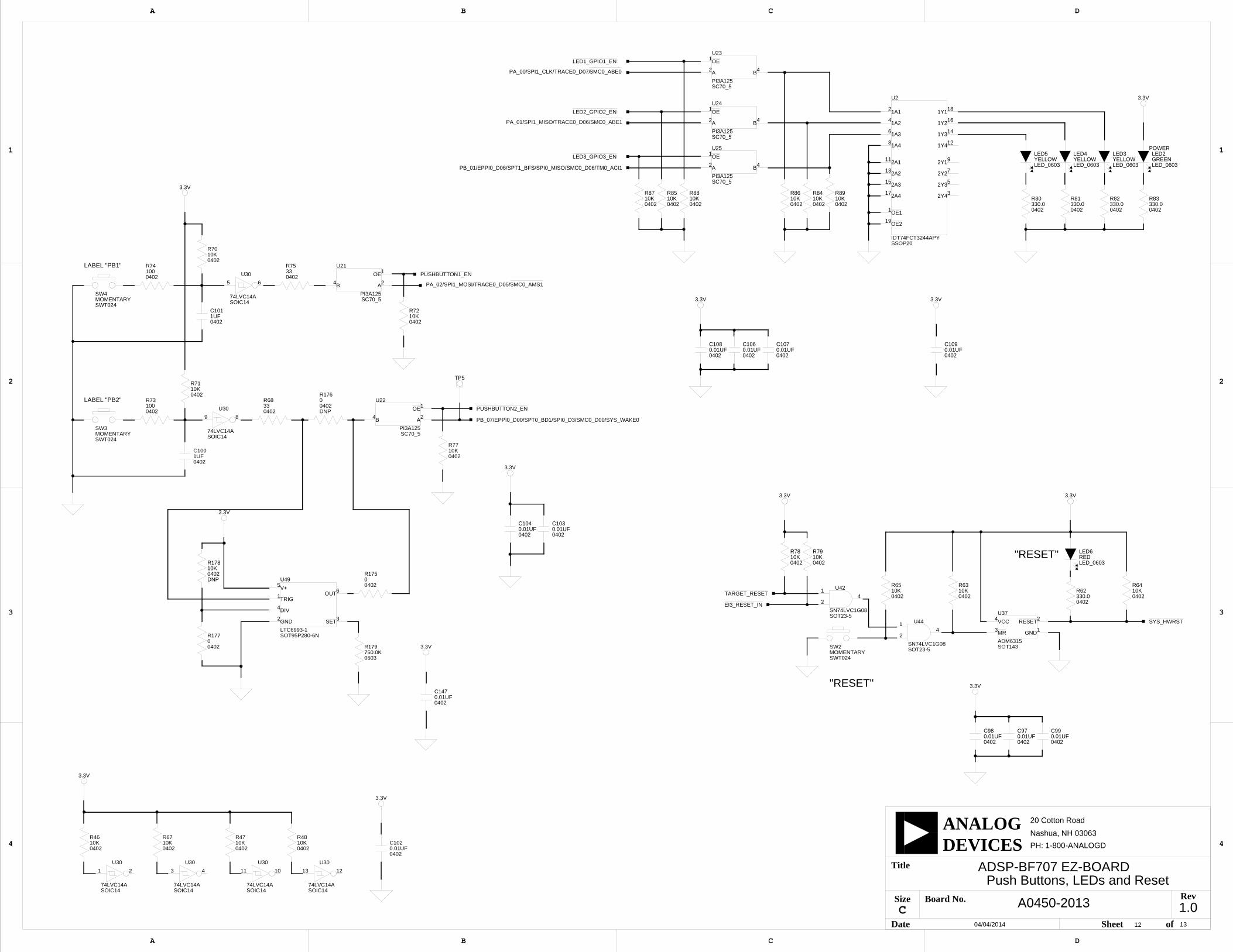
0402330.0R80
3.3V
C1060.01UF0402
C1070.01UF0402
C1080.01UF0402
OE1
B4A2
U23
SC70_5PI3A125
LED_0603YELLOWLED5
R81330.00402
R82330.00402
R83330.00402
LED2GREENLED_0603
3.3V
C1090.01UF0402
3.3V
LED3YELLOWLED_0603
LED4YELLOWLED_0603
1A1
1A2
1A3
1A4
1Y1
1Y2
1Y3
1Y4
2A1
2A2
2A3
2A4
2Y1
2Y2
2Y3
2Y4
OE1
OE2
U2
IDT74FCT3244APYSSOP20
19
1
3
5
7
9
17
15
13
11
12
14
16
18
8
6
4
2
R8410K0402
OE1
B4A2
U24
PI3A125SC70_5
R8510K0402
R8610K0402
OE1
B4A2
SC70_5PI3A125
U25
R87
040210K
R8810K0402 0402
10KR89
LED6REDLED_0603
42
1 U44
SN74LVC1G08SOT23-5
R62
0402330.0
R63
040210K
3.3V
R64
040210K
R65
040210K
42
1 U42
SN74LVC1G08SOT23-5
C970.01UF0402
C980.01UF0402
3.3V
C990.01UF0402
SW2MOMENTARYSWT024
10K0402
R78
R6710K0402
U30
74LVC14ASOIC14
43
OE
B A
U21
PI3A125SC70_5
24
1
OE
B A
U22
PI3A125SC70_5
24
1
U30
74LVC14ASOIC14
65
R68330402U30
74LVC14ASOIC14
89
R70
040210K
3.3V
C1001UF0402
C1011UF0402
R71
040210K
R72
040210K
R731000402
C1020.01UF0402
R741000402
R75330402
TP5
SW3MOMENTARYSWT024
R77
040210K
SW4MOMENTARYSWT024
3.3V
C103
04020.01UF
3.3V
C104
04020.01UF
D
4
3
2
1
A B C
20 Cotton Road
Nashua, NH 03063
A B C D
4
3
2
1
PH: 1-800-ANALOGD
C
Title
Size Board No.
Date Sheet of
DEVICESANALOG
Rev1.013
A0450-2013
ADSP-BF707 EZ-BOARD
04/04/2014
Push Buttons, LEDs and Reset
12
3.3V
10K0402
R79
3.3V
MR
RESET
GND
VCC
U37
ADM6315SOT143
4
1
2
3
R175
04020
DNP
R176
04020
R17700402
DNP
10K0402
R178
R179750.0K0603
3.3V
0.01UF0402
C147
SET
V+
DIV
OUT
GND
TRIG
U49
LTC6993-1SOT95P280-6N
1
2
6
4
5
3
LED1_GPIO1_EN
LED2_GPIO2_EN
LED3_GPIO3_EN
SYS_HWRST
PUSHBUTTON2_EN
PUSHBUTTON1_EN
PA_00/SPI1_CLK/TRACE0_D07/SMC0_ABE0
PA_01/SPI1_MISO/TRACE0_D06/SMC0_ABE1
PA_02/SPI1_MOSI/TRACE0_D05/SMC0_AMS1
PB_01/EPPI0_D06/SPT1_BFS/SPI0_MISO/SMC0_D06/TM0_ACI1
PB_07/EPPI0_D00/SPT0_BD1/SPI0_D3/SMC0_D00/SYS_WAKE0
POWER
"RESET"
"RESET"
LABEL "PB1"
LABEL "PB2"
1 2
74LVC14ASOIC14
U30
11 10
SOIC14
U30
74LVC14A
13 12
U30
74LVC14ASOIC14
040210KR46
040210KR47
040210KR48
3.3V
TARGET_RESET
EI3_RESET_IN

5V
POWER
P13
CON045
2
3
1
SHGND
SHGND
F1
FUS0043A
D7
SMC
MBRS540T3G
FER6
FER002190
2
3
1
4
C112
12061000PF
D2
SOT23-3
GSOT05
FER4
1206600
C113
121010UF
FER5
1206600
C114
12061000PF
GP1LOOP_2838
TP13TP14TP15TP16TP17
JUMPERSHORTING
DEFAULT=INSTALLED
SJ5
TP1810K0402DNP
R107
TP6
3.3V
DNP
10K0402
R108
FLG
IN1 OUT1
OUT2
GND
EN
MIC2025-1SOIC8
U40
1
3
8
67
2
1UF0805
C115150UFD
CT11UF0805
C116
00402
R111
0.051206
R112
5V
3.3V
3.3V
JUMPERSHORTING
DEFAULT=INSTALLED
SJ1
04020.01UFC110
3.3V
L11UHIND_LQH32P
04020.01UFC111
P9
IDC2X1
1 23.3V
R105
12060.05
P10
IDC2X1
1 2
R106
12060.05
IN+
GND
IN-
EPAD
SCL
SDA
ALERT
A0A1
VS
BUS
U31
INA230QFN50P300X300-17N
11
9
12
3
4
5
17
12
10
13
5V
0R104DNP0402
R109
040210K
DNP
R110
040210K
040210.0KR118
C11810UF0603
L21UHINDC2016
AGND1
EN2
EN1
EPAD
AGND2
AGND3
AGND4
AGND5
VOUT1
VIN2
VIN1
PGND2
NC
MODE
PGND1
AVIN
VIN3
EN3
VOUT3
SW1
FB1
FB2
SW2
VOUT2
FB3
BUCK1
BUCK2
LDO
VR1
ADP5024QFN50P400X400-25N
19
9
4
8
11
15
20
22
21
17
14
13
6
5
16
3
10
2423182 25
12
7
1
040212.0KR116
DNP
R9310K0402
040210KR103
3.3V
040239.0KR117 IDC2X1
P121 2
040215.0KR119R113
10.0K0402
R101 56.0K0402
C11910UF0603
C1201UF0603
C1214.7UF0805
C1224.7UF0805
R114 00402
R11500402DNP
IN-2
VPU
IN+3
IN+1
GND
IN-3
IN+2
IN-1
EPAD
PV
SCL
SDA
CRITICALWARNING
A0
TC
VS
U48
INA3221QFN65P400X400-17N
4
13
5
89
7
6
10
17
11
15
1
3
12
2
16
14
0.051206
R120
IDC2X1
P81 2
0.051206
R92
3.3VR9410K0402DNP
R9510K0402
R9610K0402
R9710K0402
040210KR100
3.3V
040210KR98
040210KR99
D
4
3
2
1
A B C
20 Cotton Road
Nashua, NH 03063
A B C D
4
3
2
1
PH: 1-800-ANALOGD
C
Title
Size Board No.
Date Sheet of
DEVICESANALOG
Rev1.013
A0450-2013
ADSP-BF707 EZ-BOARD
04/04/2014
Power
13
04020R102DNP
3.3V
P11
IDC2X1
1 2
JUMPERSHORTING
DEFAULT=INSTALLED
SJ2
JUMPERSHORTING
DEFAULT=INSTALLED
SJ3
JUMPERSHORTING
DEFAULT=INSTALLED
SJ4
TP10
TP11
TP12
VDD_INT
VDD_INT
VDD_EXT
VDD_EXTSYS_EXTWAKE
PB_02/EPPI0_D05/SPT1_BD0/SPI0_MOSI/SMC0_D05
PB_03/EPPI0_D04/SPT1_BD1/SPI0_D2/SMC0_D04
USB0_VBUS
USB0_VBC
TWI0_SCL
TWI0_SCLTWI0_SDA
TWI0_SDAVDD_INT_SOURCE
VDD_INT_SOURCE
VDD_DMC0_SOURCE
VDD_DMC0_SOURCE
VDD_DMC0
VDD_DMC0
3V_SOURCE
3V_SOURCE
3V_SOURCE
USB0_VBUS_EN
USB0_VBUS_EN
"5V"
GND Test Points are scattered on PCB for Test Measurement Purposes.
LABEL "GND" ON ALL TPs
"USB0_VBUS"
Remove P11 when measuring USB_VBUS
"VDD_EXT"
"3.3V"
Remove jumpers when measuring power1.1V
1.8V
TWI address 1000 001x
where x is the R/W bit. Read - 1, Write - 0
"VDD_INT"
"VDD_DMC0"
DNP
060310UFC117
0.1UF0402
C152
TWI address 1000 000x
where x is the R/W bit. Read - 1, Write - 0
C82
06031UF

ADSP-BF707 EZ-KIT Lite Evaluation System Manual I-1
I INDEX
AADSP-BF707 processor, xarchitecture, of this EZ-KIT Lite, 2-2
Bbill of materials, A-1board schematic (ADSP-BF707), B-1boot mode select switch (SW1), 2-17bus switch, 2-5
example, 2-6
CCAN0 connector (J4), 2-24CAN0 interface, 1-10CAN1 connector (J5), 2-25CAN1 interface, 1-11configuration, of this EZ-KIT Lite, 1-3connectors, 2-21
diagram of locations, 2-21J3 (RF wireless), 2-23J4 (CAN0), 2-24J5 (CAN1), 2-25J6 (SD), 2-24J7, J8, J9 (HADC SMC), 2-23JP1 (HADC), 2-24P13 (power), 2-22P1A-C (expansion interface III), 2-22P2 (TRACE and JTAG/SWD/SWO), 2-25P3 (JTAG/SWD/SWO), 2-25
connectors (continued)P5 (USB), 2-23P6 (USB to UART), 2-22
contents, of this EZ-KIT Lite package, 1-2
DDDR2 memory, 1-8debug interface, 1-12default configuration, of this EZ-KIT Lite, 1-3default jumper and switch settings, 1-4default processor interface availability, 2-7design reference information, 1-15
EEngineerZone, xviievaluation license, 1-8example programs, 1-14expansion interface, 1-13expansion interface III connectors (P1A-C),
2-22
FFET switches, 2-4
example, 2-4
Ggeneral-purpose I/O pins (GPIO), 2-20GPIO LEDs (LED3-5), 2-20GPIO push buttons switches (SW3-4), 2-17

Index
I-2 ADSP-BF707 EZ-KIT Lite Evaluation System Manual
HHADC, 1-10HADC connector (JP1), 2-24HADC SMC connectors (J7, J8, J9), 2-23housekeeping ADC, 1-10
Iinstallation, of this EZ-KIT Lite, 1-4, 1-5interface
CAN0, 1-10CAN1, 1-11debug, 1-12SD, 1-12UART0, 1-10USB, 1-11
JJTAG/SWD/SWO connector (P3), 2-25jumpers
diagram of locations, 2-18
LLEDs, 2-19
diagram of locations, 2-19LED1 (SYS_FAULT), 2-20LED2 (power), 2-20LED3-5 (GPIO), 2-20LED6 (reset), 2-20
license restrictions, 1-8
Mmechanical switch, 2-5, 2-7
Nnotation conventions, xvii
Ppackage contents, 1-2power
architecture, 1-13LED (LED2), 2-20measurements, 1-14
power connector (P13), 2-22power jumpers, listing, 2-18power jumpers (P8-12, P14-18), 2-18power-on-self test (POST), 1-12product overview, xprogramming SoftConfig switches, 2-8push buttons and switches, 2-16
Rreset LED (LED6), 2-20reset push button switch (SW2), 2-17RF wireless connector (J3), 2-23
Sschematic, of ADSP-BF707 EZ-KIT Lite, B-1SD connector (J6), 2-24SD interface, 1-12SoftConfig
on the EZ-KIT Lite, 2-7, 2-10overview, 2-3programming switches, 2-8
SPI flash, 1-9startup, of this EZ-KIT Lite, 1-6supported tools, xviswitches
programming SoftConfig, 2-8SW1 (boot mode select), 2-17SW2 (reset push button), 2-17SW3-4 (GPIO push buttons), 2-17
switches, diagram of locations, 2-16SYS_FAULT LED (LED1), 2-20system architecture, of this EZ-KIT Lite, 2-2

ADSP-BF707 EZ-KIT Lite Evaluation System Manual I-3
Index
Ttechnical support, xvTRACE and JTAG/SWD/SWO connector
(P2), 2-25
UUART0 interface, 1-10USB connector (P5), 2-23USB interface, 1-11USB to UART connector (P6), 2-22

Index
I-4 ADSP-BF707 EZ-KIT Lite Evaluation System Manual

Mouser Electronics
Authorized Distributor
Click to View Pricing, Inventory, Delivery & Lifecycle Information: Analog Devices Inc.:
ADZS-BF707-EZBRD